


Abstract
Memristive devices have emerged as promising candidates for next-generation non-volatile memory and neuromorphic computing systems owing to their simple device architecture, low power consumption, and capability for analog conductance modulation. In this work, Fe2O3-incorporated TiO2 thin films were employed as the active switching layer to investigate their resistive switching and artificial synaptic characteristics. The fabricated Ag/TiO2 + Fe2O3/FTO device exhibits stable switching performance with a low operating voltage of approximately ±0.6 V, a large ON/OFF ratio of ~103, retention of nearly 104 s, and endurance over 5000 pulse cycles, representing a significant improvement compared with pristine TiO2 devices. Electrical transport analysis demonstrates Schottky emission-dominated conduction in the high-resistance state and Ohmic conduction in the low-resistance state. Furthermore, analog switching behavior was achieved by operating the device under a higher compliance current, demonstrating gradual conductance modulation and synaptic weight update characteristics, indicating the potential of the device for neuromorphic applications. These results demonstrate that Fe2O3 incorporation provides an effective approach for simultaneously enhancing memory performance and synaptic functionality in TiO2-based memristors, highlighting their potential for future memory and neuromorphic computing applications.
1. Introduction
Artificial intelligence and deep neural networks have achieved remarkable success across domains from image recognition and natural language processing to autonomous systems and scientific data analysis [1,2]. Despite these advances, the computational efficiency of modern neural networks is severely constrained by the conventional von Neumann architecture, where memory and processing units are physically separated. The continuous data shuttling between these units results in substantial energy consumption and latency, commonly referred to as the von Neumann bottleneck. This challenge is further exacerbated by the diminishing returns of conventional CMOS scaling as transistor dimensions approach their physical limits, leading to increasing computation costs for training and deploying large-scale neural networks [3,4,5]. To overcome these limitations, there is growing interest in developing electronic devices capable of simultaneously performing storage and computation in a manner analogous to biological neural systems. Neuromorphic computing, inspired by the massively parallel, event-driven architecture of the human brain, offers a transformative paradigm by co-locating memory and computation within a single hardware platform, enabling highly efficient learning and inference operations [6,7,8]. Translating this functionality requires artificial synaptic devices capable of emulating key biological synaptic functions including analog and multi-level conductance modulation, long-term potentiation (LTP), long-term depression (LTD), and energy-efficient synaptic weight update operations within a simple, compact device structure.
To realize neuromorphic hardware capable of overcoming the limitations of conventional computing architectures, several emerging non-volatile memory technologies have been explored owing to their nonlinear electrical characteristics and electrically programmable resistance states [4,9]. Among these, resistive random-access memory (RRAM) devices have emerged as one of the most promising hardware platforms owing to their simple two-terminal architecture, fast switching speeds, low operating voltage, high scalability, and ability to emulate synaptic weight modulation through analog resistance changes [8,9,10]. In oxide-based RRAM devices, resistive switching generally originates from the reversible formation and rupture of conductive pathways induced by electrically driven migration of metal ions and/or oxygen vacancies under an applied electric field. Among various metal oxides investigated as switching materials, titanium dioxide (TiO2) stands out due to its notable attributes including wide bandgap (~3.2 eV), excellent chemical stability, CMOS compatibility, facile fabrication, and defect-mediated switching characteristics [11,12,13]. The resistive switching behavior of TiO2 is critically associated with the evolution and redistribution of electrically active ionic defects, which facilitate the conductive filament nucleation and dissolution within the oxide matrix, enabling reversible modulation of resistance states [12,13]. Nevertheless, the stochastic nature of filament formation and dissolution often limits switching reliability and conductance controllability required for practical memory and neuromorphic applications. To address this limitation, various defect engineering strategies including interfacial modification, dopant incorporation, and composite active-layer design have been widely adopted to regulate defect dynamics and improve switching stability [14].
Recently, incorporation of secondary functional materials into the active switching layer has emerged as an effective approach to tailor the switching performance of memristive devices [15,16,17,18]. Such compositional modification can alter the device’s local defect dynamics, charge transport pathways, and conductive filament evolution within the oxide layer. For example, incorporation of Al-doped ZnO into TiO2 has been reported to induce transitions between analog and digital switching modes [15], while MnO2–TiO2 nanocomposites have demonstrated distinct switching characteristics arising from changes in ion–electron interactions and filament formation processes [16]. In addition, Li et al. reported improved switching uniformity and retention characteristics by introducing MoS2 quantum dots in the ZnO switching layer [17]. These studies collectively demonstrate that the incorporation of secondary functional materials provides a versatile route for regulating defect-mediated transport phenomena in oxide-based memristive systems. Among various transition-metal oxides, Fe2O3 is particularly attractive because of its chemical stability, mixed Fe2+/Fe3+ valence states, and oxygen vacancy-related defect chemistry, which can significantly influence defect-assisted conduction processes [19,20]. Moreover, Fe2O3 and TiO2 are two chemically stable transition-metal oxides that have been extensively investigated in photocatalysis, electrochemistry, and electronic devices owing to their rich defect chemistry and tunable electronic structures [21,22]. Previous studies have shown distinct switching behavior depending on the thickness of the Fe2O3 switching layer [19]. Furthermore, Fe2O3–TiO2 composites have been extensively investigated in photocatalytic systems, where Fe2O3 incorporation has been shown to modify the electronic structure and interfacial charge-transfer characteristics of TiO2 [23]. These observations suggest that compositional engineering of TiO2 using Fe2O3 may provide an effective route for tailoring defect-assisted conduction and resistive switching behavior.
While previous studies have primarily focused on enhancing resistive switching through multilayer architectures, heterostructure engineering, or the incorporation of secondary materials [24,25,26,27], the influence of Fe2O3 incorporation on the switching reliability and neuromorphic characteristics of TiO2-based memristors has remained comparatively less explored. Motivated by these considerations, the present work investigates the influence of 1 wt% Fe2O3-incorporation on the resistive switching and neuromorphic characteristics of TiO2 memristive devices. Therefore, a relatively low concentration of Fe2O3 (1 wt%) was intentionally selected as an initial proof-of-concept composition to introduce Fe-related defect states while preserving the TiO2 switching matrix. Ag/TiO2 + Fe2O3/FTO devices were fabricated and systematically characterized through electrical, structural, and chemical analyses, with pure TiO2-based devices serving as a reference for comparison. X-ray photoelectron spectroscopy was employed to understand the evolution of electronic states and defect configurations within the active layer. The study demonstrates that such a simple compositional engineering strategy effectively enhances resistive switching performance, resulting in a large ON/OFF resistance ratio (~103), reduced and more uniform switching voltages, improved endurance (5 × 10³ cycles), stable retention (~104 s), and low switching energy. In addition, by appropriately controlling the operating conditions, the same device exhibits analog potentiation and depression characteristics, demonstrating its potential for neuromorphic computing applications. The results provide insight into the role of iron-oxide-induced defect engineering in governing memory and neuromorphic functionalities in TiO2-based oxide memristors.
2. Results and Discussion
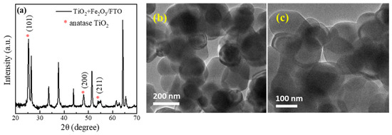
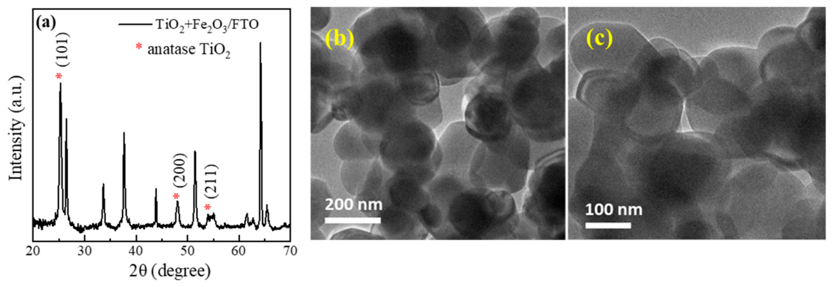
Figure 1a shows the XRD pattern of the composite film deposited on FTO glass. To distinguish film peaks from substrate contributions, the pattern was compared directly with that of the bare FTO substrate. This comparison reveals that most diffraction peaks in the TiO2/FTO pattern originate from the underlying FTO layer, which is expected given the relatively thin TiO2 coating. Only three peaks—at 2θ = 25.31°, 48.02°, and 53.96°—are absent in the bare FTO reference and are therefore unambiguously attributed to TiO2 anatase (101), (200), and (211), respectively. No additional diffraction peaks corresponding to crystalline Fe2O3 or other iron oxide phases were detected within the sensitivity of the XRD measurement. This observation is consistent with the low Fe2O3 concentration (1 wt%), although the spatial distribution of Fe2O3 nanoparticles cannot be determined from XRD alone. Similar observations have also been reported for low-concentration Fe2O3-incorporated TiO2 systems in the literature [28]. Figure 1b,c present TEM images of TiO2 and TiO2 + Fe2O3 films having spherical-shaped nanoparticles of approximately 50–150 nm. Both films consist of agglomerated nanoparticles with comparable morphological characteristics. No significant change in particle morphology is observed following Fe2O3 incorporation, suggesting that the addition of Fe2O3 does not drastically alter the overall microstructure of the TiO2 matrix. However, a slightly increased degree of particle interconnection can be observed in the Fe2O3-incorporated sample, which may facilitate charge transport across neighboring particles.
Figure 1.
(a) XRD patterns of TiO2 + Fe2O3 thin films deposited on FTO-coated glass substrates. Anatase TiO2 peaks are indicated with a red asterisk. No additional peaks attributable to iron oxide phases are observed in the composite film. Non-indexed peaks correspond to the FTO bottom electrode. (b,c) TEM image of TiO2 and iron oxide incorporated TiO2 film having spherical-shaped nanoparticles of approximately 50–150 nm.
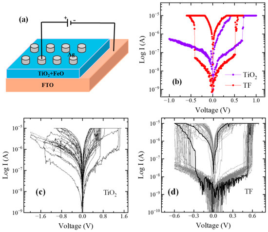
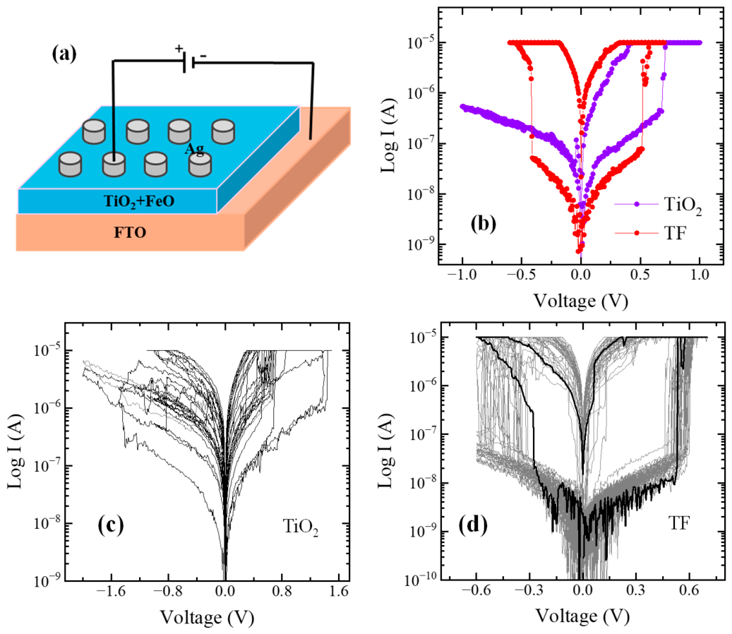
Figure 2 presents the device architecture and electrical switching characteristics of the fabricated devices. The schematic in Figure 2a illustrates the Ag/TiO2 + Fe2O3/FTO device structure, comprising Ag top electrodes and an FTO bottom electrode. Figure 2b shows the typical semi-logarithmic current-voltage (I–V) characteristics of both Ag/TiO2/FTO and Ag/TiO2 + Fe2O3/FTO (TF) devices measured under DC voltage sweeps of ±1 V and ±0.6 V, respectively, with a compliance current of ~10 µA. Prior to switching, both devices required an initial electroforming process to establish the initial current conductive pathway through the active switching layer. Although the electroforming process reduced the initial device resistance, the devices remained in the high-resistance state (HRS). During the subsequent voltage sweep (0 V → +1 V → −1 V → 0 V), the I–V characteristics exhibited a typical bipolar hysteresis loop. Under positive bias, the devices switched from the HRS to the low-resistance state (LRS) through the SET process, while a compliance current of 10 μA was maintained to prevent excessive filament growth and permanent dielectric breakdown. A subsequent negative voltage sweep induced the RESET process, returning the devices from the LRS to the HRS and completing one bipolar switching cycle. Significant differences are evident between the two devices in terms of switching voltage, resistance window, and switching characteristics.
Figure 2.
(a) Schematic of Ag/TiO2 + Fe2O3/FTO (TF) device configuration. Here, Ag and fluorine-doped tin oxide (FTO) were used as the top and bottom electrodes, respectively. The top electrode was formed using manually applied Ag epoxy contacts. (b) Semi-logarithmic I–V characteristics of Ag/TiO2/FTO (purple) and Ag/TiO2 + Fe2O3/FTO (red) devices measured over ±1 V with a compliance current of 10 µA. Prior to bipolar resistive switching, an initial electroforming process was performed by applying a positive voltage sweep up to 2 V under a compliance current of 10 μA. The arrows indicate the voltage sweep direction. The cycling variability of the (c) Ag/TiO2/FTO and (d) Ag/TiO2 + Fe2O3/FTO (TF) devices demonstrates the improved stability and consistent switching in the Fe2O3-incorporated device. The black curve highlights the first switching cycle, while the grey curves represent the subsequent repetitive cycles.
The pure TiO2 device requires a SET voltage of 0.69 V and a RESET voltage of −1 V, with an ON/OFF resistance ratio of ~20 at a reading voltage of 0.1V, which may limit reliable discrimination between resistance states in practical memory applications due to read margin error [29,30]. In contrast, the TF device achieves SET and RESET at much lower voltages of 0.51 V and −0.42 V, respectively, with an ON/OFF ratio exceeding 3 × 10², more than one order of magnitude higher than the TiO2 device. The cycling variability of the two devices is compared in Figure 2c,d. Figure 2c shows 20 consecutive I–V sweep cycles of the TiO2 device with severe cycle-to-cycle variability. The HRS current fluctuates by nearly two decades across cycles, and the SET voltage fluctuates considerably between sweeps, reflecting non-uniform and random filament formation and dissolution; before it completely lost its memory characteristics and behaved as an ohmic resistor. In contrast, Figure 2d shows 50 consecutive switching cycles of the TF device within a considerably narrower voltage window of ±0.6 V and a stable ON/OFF resistance ratio. The consistent switching characteristics indicate robust formation and dissolution of conductive pathways under repeated electrical stress. Such stable switching behavior is essential for practical non-volatile memory and artificial synaptic applications, where reliable conductance modulation over repeated programming operations is required.
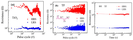
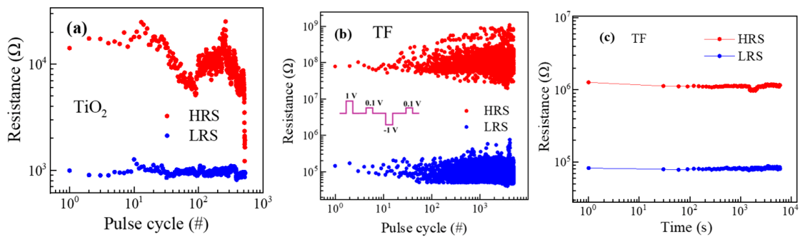
The reliability of the TF device was evaluated through pulse endurance and retention measurements. Figure 3a shows the pulse endurance characteristics of the TiO2 device measured using alternating ±1.5 V write pulses with a pulse width of 100 μs, followed by a 0.2 V read pulse of 100 μs. The pulse conditions were selected based on the operating voltage requirements of the device determined from the DC I–V characteristics, where reliable RESET operation requires a higher programming voltage. The device exhibits a narrow memory window of approximately one order of magnitude between resistance states with pronounced variation in HRS. More critically, the memory window degrades progressively and collapses irreversibly at approximately 550 pulse cycles, where the HRS resistance converges with the LRS. This endurance failure is characteristic of filament overgrowth, wherein incomplete filament dissolution during the RESET event leads to gradual growth of the residual filament, reducing the effective HRS resistance until state discrimination is lost [31]. In contrast, the endurance of the TF device was performed using alternating ±1.0 V write pulses with a pulse width of 100 μs, followed by a 0.1 V read pulse of 100 μs to monitor the resistance state. Consecutive write pulses were separated by a 1 ms interval, corresponding to a write duty cycle of 10%, as shown in Figure 3b. The lower pulse amplitude was selected according to the reduced operating voltages of the TF device, as confirmed by the DC measurement. The device demonstrates a well-defined memory window of approximately ~103 over 5000 pulse cycles. The enhanced stability suggests that Fe2O3 incorporation influences defect-assisted conduction processes and promotes more controlled conductive pathway evolution during repeated switching operations. Furthermore, retention measurements demonstrate stable memory characteristics with distinguishable resistance states preserved for nearly 104 s, as shown in Figure 3c. The combined improvements in memory window, endurance, and retention highlight the effectiveness of Fe2O3 incorporation in enhancing the operational reliability of TiO2-based memristive devices for memory and neuromorphic computing applications. Based on the improved switching behavior, we now focus on TF memristor devices in the subsequent discussion.
Figure 3.
Endurance test of (a) Ag/TiO2/FTO device performed using pulse measurement under ±1.5 V read at 0.2 V. The device exhibits a narrow memory window of approximately one order of magnitude between resistance states. The device also shows a high variation in the high-resistance state and fails to switch after 550 pulse cycles. (b) Endurance of the Ag/TiO2 + Fe2O3/FTO device over 5000 pulse cycles with a well-defined memory window of approximately ~103. Inset shows the schematic of pulse programming (±1 V read at 0.1 V) for the TF devices. (c) Retention measurements of the TF device under the same pulse condition for nearly 104 s.
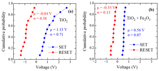
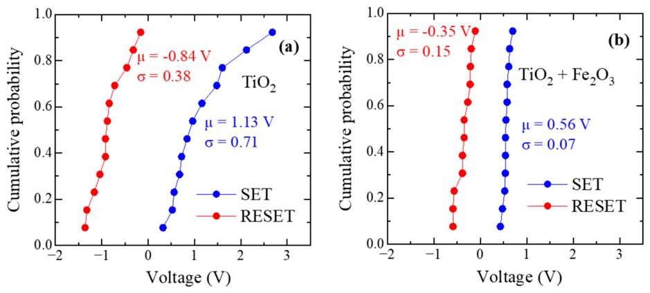
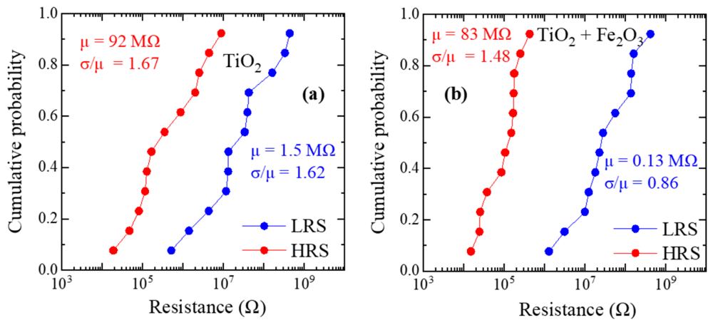
To evaluate the reproducibility of the fabricated memristors, the switching characteristics of 12 independently fabricated devices were statistically analyzed, and the cumulative probability distributions of the SET/RESET voltages and HRS/LRS resistance states are presented in Figure 4 and Figure 5, respectively. The pristine TiO2 devices exhibit relatively broad distributions of both SET and RESET voltages, with average values of 1.13 ± 0.71 V and −0.84 ± 0.38 V, respectively. In contrast, the Fe2O3-incorporated TiO2 devices demonstrate significantly improved switching uniformity, exhibiting reduced average switching voltages of 0.56 ± 0.07 V for SET and −0.35 ± 0.15 V for RESET. The markedly narrower voltage distributions indicate that Fe2O3 incorporation promotes more deterministic and reproducible filament nucleation across devices, thereby reducing the stochastic nature of resistive switching.
Figure 4.
Cumulative probability distributions of SET voltage (VSET, blue) and RESET voltage (VRESET, red) measured from 12 independently fabricated devices for (a) the pristine Ag/TiO2/FTO (T) device and (b) the Ag/TiO2 + Fe2O3/FTO (TF) device. The mean (µ) and standard deviation (σ) of each distribution are annotated. The TF device exhibits significantly tighter switching voltage distributions with = 0.56 ± 0.07 V and = −0.35 ± 0.15 V, compared to the T device ( = 1.13 ± 0.71 V; = −0.84 ± 0.38 V), demonstrating markedly improved device-to-device switching voltage uniformity upon Fe2O3 incorporation.
Figure 5.
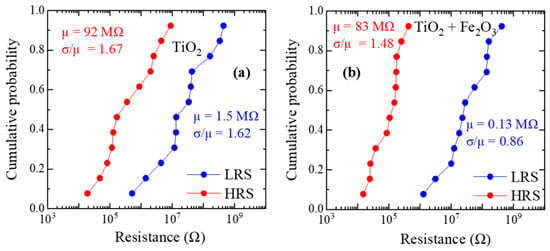
Cumulative probability distributions of the high resistance state (HRS, red) and low resistance state (LRS, blue) resistances measured from 12 independently fabricated devices for (a) the pristine Ag/TiO2/FTO (T) device and (b) the Ag/TiO2 + Fe2O3/FTO (TF) device. The mean resistance (µ) and coefficient of variation (σ/µ) are annotated for each distribution. The TF device exhibits a substantially lower mean LRS resistance ( = 0.13 MΩ, σ/µ = 0.86) compared to the T device ( = 1.5 MΩ, σ/µ = 1.62), reflecting more complete and uniform conductive filament formation upon Fe2O3 incorporation.
A similar trend is observed in the resistance distributions shown in Figure 5. While the average HRS remains nearly unchanged, indicating that Fe2O3 incorporation does not compromise the insulating state, the average LRS decreases significantly from 1.5 MΩ for pristine TiO2 to 0.13 MΩ for the TF device. Moreover, the relative variation in the LRS resistance (σ/μ) decreases from 1.62 to 0.86 following Fe2O3 incorporation, indicating a more uniform conductive state. The simultaneous preservation of a high HRS and stabilization of the LRS contributes to the enlarged memory window and improved cycle-to-cycle reproducibility observed in the TF devices.
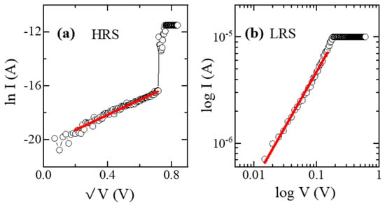
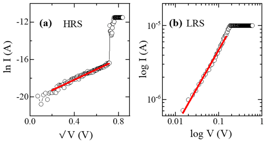
To understand the charge transport mechanisms of the Ag/TiO2 + Fe2O3/FTO (TF) device, the experimental I–V data were analyzed against various conduction mechanisms such as space charge-limited conduction, Poole-Frankel, Schottky emission, and hopping conduction. It was confirmed that, in the HRS, ln(I) varies linearly with V½ over the applied voltage range prior to the SET transition, which is the characteristic signature of Schottky emission, suggesting that charge transport is dominated by thermionic emission across the metal-oxide interface. Upon application of a sufficient electric field, defect migration and conductive pathway formation reduce the effective barrier for carrier transport, resulting in a transition to the LRS [32]. In the LRS (Figure 6b), the log(I)–log(V) relationship is linear with a slope of ~1, confirming Ohmic conduction through the fully formed metallic Ag conductive filament [33].
Figure 6.
Charge transport mechanisms of the Ag/TiO2 + Fe2O3/FTO (TF) device. (a) HRS follows Schottky emission conduction and (b) LRS indicates Ohmic nature. The solid lines represent the corresponding fitting curves, while the black symbols denote the experimental data.
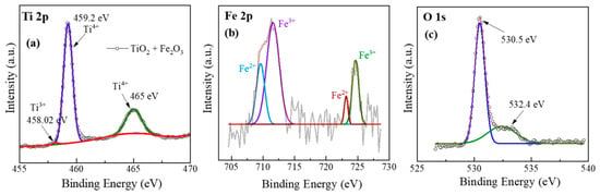
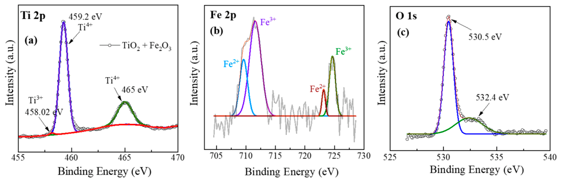
To further elucidate the origin of the enhanced switching performance of the Fe2O3-incorporated device, the composition and chemical bonding states of both films in the pristine state were investigated using X-ray photoelectron spectroscopy (XPS). All the peaks were fitted with Gaussian functions after a Shirley background subtraction. Figure 7 illustrates the high-resolution Ti 2p, Fe 2p, and O 1s core-level spectra of the TF device. The Ti 2p spectrum of the pristine TiO2 film (Supplementary Figure S1a) consists of a characteristic doublet corresponding to the 2 and 2 components located at 459.3 eV and 465.1 eV, respectively, with a spin–orbit splitting of 5.8 eV. The peak position and peak separation confirm the main oxidation state of Ti is 4+ [34,35]. After Fe2O3 incorporation, the primary Ti4+ peaks remain essentially unchanged, indicating preservation of the TiO2 framework. However, an additional weak shoulder peak centered at ~458.02 eV is observed, which is attributed to lower oxidation states (Ti3+) of Ti, as shown in Figure 7a [19,20]. Quantitative peak fitting indicates that the Ti3+ component accounts for approximately 0.96% of the total Ti species, while Ti4+ remains the dominant oxidation state (99.04%). The presence of this weak Ti3+ component is generally associated with oxygen-vacancy-related defect states arising from the partial reduction of Ti4+ in TiO2-based materials [36,37,38], while the predominance of Ti4+ indicates that the TiO2 chemical environment remains preserved after Fe2O3 incorporation.
Figure 7.
High-resolution XPS spectra of the TiO2 + Fe2O3 film showing (a) Ti 2p, (b) Fe 2p, and (c) O 1s core level spectra. The Ti 2p spectrum reveals the presence of Ti4+ and Ti3+ states, while the Fe 2p spectrum exhibits mixed Fe2+ and Fe3+ oxidation states, indicating the coexistence of multiple Fe valence states together with lattice and defect-related oxygen components within the active layer.
Figure 7b shows the Fe 2p spectrum of the TF film. Two characteristic peaks centered at binding energies of 711.57 eV and 724.64 eV are attributed to Fe 2 and Fe 2, respectively, assigned to Fe3+ oxidation state, whereas peaks at 709.64 and 723.15 eV correspond to Fe2+ [23,38]. Quantitative deconvolution indicates that 71.5% of the Fe species exist as Fe3+ and 28.5% as Fe2+. The coexistence of Fe2+ and Fe3+ indicates a mixed-valence environment within the oxide matrix. When considered together with the Ti3+ component observed in the Ti 2p spectrum, these results suggest that Fe2O3 incorporation is expected to influence the local defect chemistry and electronic structure of the oxide matrix.
To further investigate the oxygen chemical states, O 1s spectra of both pristine TiO2 and TF films were analyzed. As shown in Supplementary Figure S1c, the pristine TiO2 film exhibits a dominant peak centered at ~530.5 eV, which is attributed to lattice oxygen (O2−). In addition, a higher binding energy component is observed at ~532.2 eV, which is commonly associated with oxygen-defect-related surface species in TiO2 [36,38]. Following Fe2O3 incorporation, this component exhibits a slight positive shift to approximately 532.4 eV, as shown in Figure 7c. Quantitative peak fitting indicates that the lattice oxygen component decreases from 71.6% in pristine TiO2 to 69.8% in the TF film, while the higher binding-energy component increases from 28.4% to 30.2%, indicating a modest increase in oxygen-defect-related surface species following Fe2O3 incorporation. Collectively, the Ti 2p, Fe 2p, and O 1s analyses consistently indicate that Fe2O3 incorporation modifies the local chemical environment and defect chemistry of the TiO2 matrix. These compositional changes provide a plausible explanation for the statistically improved switching characteristics of the TF device, including reduced and more uniform switching voltages, enhanced endurance, improved retention, and a larger ON/OFF resistance ratio.
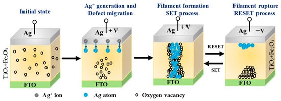
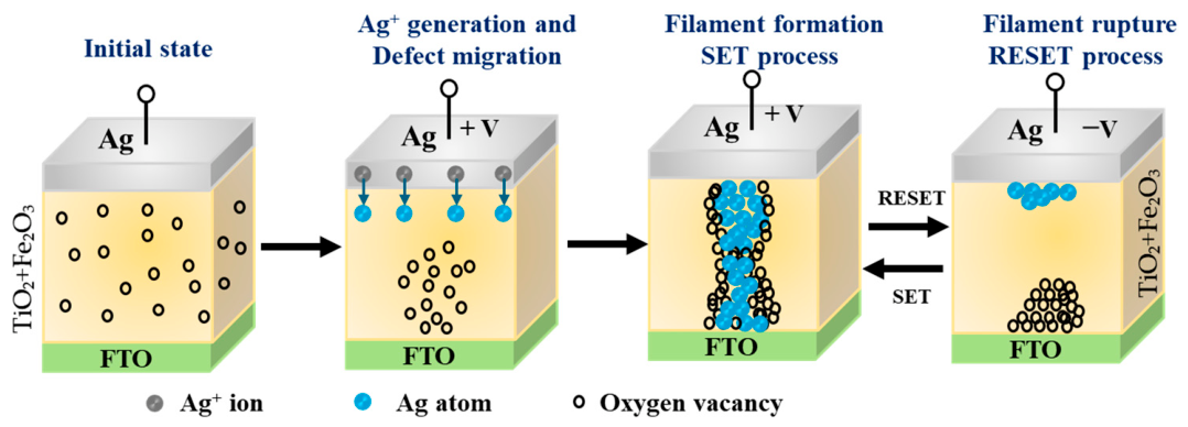
Based on the electrical transport analysis, conduction mechanism analysis, and XPS investigations, a hybrid filamentary switching mechanism is proposed for the Ag/TiO2 + Fe2O3/FTO device, as shown in Figure 8. In the pristine state, the active layer is considered to contain an electronically active defect environment associated with oxygen-deficient regions, as suggested by the coexistence of Ti3+ and mixed Fe2+/Fe3+ species observed in the XPS analysis. Although the present results do not directly establish substitutional incorporation of Fe into the TiO2 lattice, the Fe2O3 incorporation is expected to modify the local defect chemistry of the TiO2 matrix, thereby influencing the subsequent resistive switching process. Upon application of a positive bias to the Ag electrode, Ag atoms undergo electrochemical oxidation (Ag → Ag+ + e−) to form mobile Ag+ ions, which migrate into the active layer under the applied electric field. Simultaneously, oxygen vacancies redistribute within the oxide layer and accumulate near the bottom FTO electrode. As the applied voltage increases, Ag+ ions are progressively reduced and accumulated within oxygen-vacancy-rich regions, resulting in the gradual formation of a hybrid conductive filament consisting of metallic Ag atoms and oxygen defect-assisted conduction channels. The establishment of this proposed hybrid filament facilitates the transition of the device from the high-resistance state (HRS) to the low-resistance state (LRS).
Figure 8.
Schematic illustration of the proposed hybrid filamentary resistive switching mechanism in the Ag/TiO2 + Fe2O3/FTO device. In the pristine state, oxygen vacancies () are randomly distributed within the active layer and no conductive pathway exists. Upon application of a positive bias to the Ag top electrode, Ag atoms are oxidized into Ag+ ions and drift toward the FTO bottom electrode, while oxygen vacancies simultaneously migrate under the applied electric field. The accumulation of Ag species and oxygen-vacancy-rich regions leads to the formation of a hybrid conductive filament, switching the device to the low-resistance state (LRS). Under reverse bias, the Ag filament partially dissolves and oxygen vacancies redistribute, causing rupture of the conductive pathway and restoration of the HRS.
Having established switching characteristics in the TF memristor device, we next explored its potential as an artificial synaptic device for neuromorphic computing applications. Although the device exhibited stable bipolar resistive switching, the abrupt transition between the resistance states resulted in digital-type switching behavior. Such binary conductance changes are well-suited for non-volatile memory applications but undesirable for artificial synapses because biological synapses regulate information processing through gradual and continuous modulation of synaptic weights. Therefore, achieving analog conductance tuning is a prerequisite for implementing learning and memory functions in hardware neural networks [39]. Therefore, to modulate gradual conductance evolution, the device operation was optimized by increasing the compliance current from 10 μA to 10 mA. The I–V characteristics exhibit gradual and continuous resistance modulation without abrupt SET or RESET transitions under higher compliance current, as shown in Supplementary Figure S2. This transition could be attributed to the nucleation and growth of multiple conductive filaments simultaneously or the formation of a thicker filament at higher compliance, enabling partial filament formation and dissolution under applied bias [40,41].
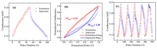
Subsequently, pulse-programming measurements were performed to emulate synaptic weight update behavior. The device conductance was evaluated by applying continuous square pulses of amplitude ± 0.8 V and pulse width of 100 μs, with a read voltage of 0.1 V after each pulse. The device demonstrates both potentiation—a gradual, incremental increase in device conductance under successive positive pulses analogous to long-term potentiation (LTP) in biological synapses—and depression—a gradual decrease in conductance under reverse polarity pulses analogous to long-term depression (LTD) [6,42]. Figure 9a presents the conductance as a function of pulse number for a complete potentiation–depression cycle. The device conductance increases continuously from 120 μS to 240 μS during the potentiation pulses, and a similar progressive decrease during depression pulse stimulation. The potentiation behavior was found to be fairly linear, but depression conductance showed a relatively sudden decrease in current for the first few pulses. Such a quick change/decrease in current led to nonlinear depression and asymmetric conductance update.
Figure 9.
Synaptic weight modulation characteristics of the Ag/TiO2 + Fe2O3/FTO memristive device. (a) Conductance evolution during potentiation (red symbols) and depression (blue symbols) processes under a consecutive square pulse voltage of ±0.8 V and pulse width of 100 μs. (b) Nonlinearity fitting of the potentiation and depression characteristics, yielding nonlinearity factors (NL) of 0.52 and 1.38, respectively. (c) Conductance modulation of potentiation/depression characteristics measured over multiple cycles, demonstrating reproducible and stable conductance evolution.
In an ideal artificial synapse, each pulse induces an identical conductance update, which is a critical figure of merit for neuromorphic learning because it directly influences the accuracy of weight updates during neural network training [34,43]. However, experimentally measured conductance updates often deviate from this ideal condition. To evaluate this nonlinearity in the TF memristor device, conductance change with pulses can be modeled using the following equations [44].
where and are potentiation and depression conductance, respectively. , and are maximum, minimum conductance, and maximum pulse number. A represents the non-linear behavior of the conductance change, and its value closer to 0 indicates more linearity.
The non-linearity (NL) values extracted from the fitting of the normalized conductance curves are 0.52 for potentiation and 1.38 for depression, as shown in Figure 9b. The potentiation non-linearity indicates a nearly linear conductance increase and a moderately asymmetric conductance decrease during depression behavior. This could be attributed to the inherently different kinetics of filament during potentiation and electrochemical dissolution during depression. Figure 9c shows the repeatable multiple training cycles of the synaptic weight, demonstrating good reproducibility of the weight update behavior. Based on the applied programming pulse conditions, the programming energy was estimated to be approximately 7.7 nJ per synaptic update. For comparison, the key performance metrics of the present device are summarized, including programming energy, with representative memristive devices in Table 1. Although further optimization is required to reduce the energy consumption to the level of state-of-the-art nanoscale memristive devices, the present study establishes Fe2O3 incorporation as an effective strategy for improving the switching reliability and analog synaptic behavior of TiO2 memristors. Future work will focus on device miniaturization and structural optimization to further enhance energy efficiency. Overall, the observed analog switching characteristics, together with the low potentiation nonlinearity and moderate depression nonlinearity, demonstrate the potential of the TF device as an artificial synapse for energy-efficient neuromorphic computing applications.
Table 1.
Comparison of the switching performances of the present device with representative memristive devices reported in the literature.
3. Materials and Methods
To prepare the film, Fluorine-doped Tin Oxide (FTO) glass slides (purchased from Solarnix, Aubonne, Switzerland) were used as the bottom electrode and silver as the top contact for the Ag/TiO2/FTO (T) RRAM device. Prior to the film deposition, FTO substrates were cleaned by the ultrasonication method with deionized water, acetone, and 2-propanol in a subsequent manner. The resistance of FTO is approximately 15 Ω. Initially, 1 wt% iron (III) oxide nanoparticles (obtained from Sigma-Aldrich, Bengaluru, India) were thoroughly mixed with TiO2 paste (obtained from Solaronix) to obtain a homogeneous composite. Next, a thin film of the composite was deposited onto the FTO substrate by blade coating method, and afterward the film was annealed for 1 h at 400 °C. The thickness of both the TiO2 and TiO2 + Fe2O3 composite films was measured using an optical profilometer and was found to be approximately 5 μm. The top silver contact was applied using silver epoxy to complete the Ag/TiO2 + Fe2O3/FTO (TF) device stack. The diameter of the Ag-epoxy contact was measured for ten representative devices and was found to be 0.20 ± 0.05 mm, corresponding to an average contact area of approximately 3.1 × 10⁻⁴ cm2. A reference device (Ag/TiO2/FTO) using TiO2 only was fabricated under identical conditions.
X-ray diffraction (XRD) patterns were recorded using a Bruker Discover D8 (Bruker, Billerica, MA, USA) with Cu-Kα radiation (λ = 1.54 Å) over the 2θ range 20–70°. The morphology of active layers was characterized using (JEOL JEM 2100, JEOL, Akishima, Japan) transmission electron microscopy (TEM) at an accelerating voltage of 200 kV. X-ray photoelectron spectroscopy (XPS) was employed to investigate the chemical bonding states and oxygen distribution in the active layers. The binding energies were calibrated against the adventitious C 1s reference peak at 284.8 eV.
The electrical characterization of both Ag/TiO2/FTO and Ag/TiO2 + Fe2O3/FTO devices was studied at room temperature using a Keithley 2400 source meter (Tektronix, Beaverton, OR, USA) in voltage sweeping mode with a compliance limit of 10 µA. The synaptic characterization of the device was performed through pulse measurements using a Keithley 4200-SCS semiconductor characterization system combined with a 4225-PMU module (Tektronix, Beaverton, OR, USA). During all electrical measurements, positive bias was applied to the Ag top electrode, while the FTO bottom electrode was grounded. All electrical measurements were performed under ambient atmosphere at room temperature (approximately 25 °C). The electrical data presented in the manuscript were collected from different devices fabricated under identical conditions.
4. Conclusions
In summary, an Fe2O3-incorporated TiO2 memristive device with an Ag/TiO2 + Fe2O3/FTO structure was successfully developed and systematically investigated for both non-volatile memory and neuromorphic computing applications. Compared with pristine TiO2, the iron-oxide incorporated device significantly enhanced the resistive switching characteristics such as low operating voltage, large memory window, stable retention, and high endurance. XPS analysis revealed the presence of Ti3+ species together with mixed Fe2+/Fe3+ oxidation states, indicating the formation of a redox-active defect environment that modifies the defect chemistry of the TiO2 matrix. Based on the transport analysis and spectroscopic investigations, a hybrid filamentary switching mechanism involving Ag-ion migration and oxygen-vacancy redistribution is proposed, where Fe-induced defect states regulate conductive pathway evolution and improve switching stability. Furthermore, by controlling the device compliance current, gradual analog conductance modulation was achieved, enabling the emulation of key synaptic functions that constitute the fundamental building blocks of neuromorphic hardware. The combination of enhanced memory performance, stable analog switching, and favorable synaptic characteristics highlights the potential of Fe2O3-incorporated TiO2 memristors as promising candidates for next-generation non-volatile memory and neuromorphic computing systems.
Supplementary Materials
The following supporting information can be downloaded at: https://www.mdpi.com/article/10.3390/jlpea16030032/s1. Figure S1: High-resolution Ti 2p core-level XPS spectra of (a) pristine TiO2 and (b) Fe2O3-incorporated TiO2 thin films. The deconvoluted spectra reveal the characteristic Ti4+ states in both samples, while an additional Ti3+ component is observed in the Fe2O3-incorporated TiO2 film. High-resolution O 1s XPS spectra of (c) TiO2 and (d) TiO2 + Fe2O3 thin films with peak deconvolution into lattice oxygen (≈530.5 eV) and oxygen-defect-related components; Figure S2: Semi-logarithmic I–V characteristics of Ag/TiO2 + Fe2O3/FTO device demonstrating gradual and continuous resistance change under higher compliance current of 10 mA.
Funding
This research received no external funding.
Data Availability Statement
All the experimental data presented in this study are included in the article. Additional inquiries can be directed to the corresponding author.
Acknowledgments
The author would like to acknowledge the Indian Institute of Technology, Hyderabad, and UGC-DAE, CSR, Center Indore, India for research facilities and measurement support.
Conflicts of Interest
The author declares no conflicts of interest.
Abbreviations
The following abbreviations are used in this manuscript:
| RRAM | Resistive random-access memory |
| TF memristor | Ag/TiO2 + Fe2O3/FTO memristor |
| XPS | X-ray photoelectron spectroscopy |
| NL | Non-linearity |
References
- LeCun, Y.; Bengio, Y.; Hinton, G. Deep learning. Nature 2015, 521, 436–444. [Google Scholar] [CrossRef] [Scilit] [PubMed]
- Merchant, A.; Batzner, S.; Schoenholz, S.S.; Aykol, M.; Cheon, G.; Cubuk, E.D. Scaling deep learning for materials discovery. Nature 2023, 624, 80–85. [Google Scholar] [CrossRef] [Scilit] [PubMed]
- Zidan, M.A.; Strachan, J.P.; Lu, W.D. The future of electronics based on memristive systems. Nat. Electron. 2018, 1, 22–29. [Google Scholar] [CrossRef] [Scilit]
- Zhu, J.; Zhang, T.; Yang, Y.; Huang, R. A comprehensive review on emerging artificial neuromorphic devices. Appl. Phys. Rev. 2020, 7, 11312. [Google Scholar] [CrossRef] [Scilit]
- Bespalov, V.; Dyuzhev, N.; Kireev, V.Y. Possibilities and limitations of CMOS Technology for the production of various Microelectronic systems and devices. Nanobiotechnol. Rep. 2022, 17, 24–38. [Google Scholar] [CrossRef] [Scilit]
- Xia, Q.; Yang, J.J. Memristive crossbar arrays for brain-inspired computing. Nat. Mater. 2019, 18, 309–323. [Google Scholar] [CrossRef] [Scilit] [PubMed]
- Wang, Z.; Wu, H.; Burr, G.W.; Hwang, C.S.; Wang, K.L.; Xia, Q.; Yang, J.J. Resistive switching materials for information processing. Nat. Rev. Mater. 2020, 5, 173–195. [Google Scholar] [CrossRef] [Scilit]
- Ielmini, D.; Pedretti, G. Resistive switching random-access memory (RRAM): Applications and requirements for memory and computing. Chem. Rev. 2025, 125, 5584–5625. [Google Scholar] [CrossRef] [Scilit] [PubMed]
- Wan, Q.; Sharbati, M.T.; Erickson, J.R.; Du, Y.; Xiong, F. Emerging artificial synaptic devices for neuromorphic computing. Adv. Mater. Technol. 2019, 4, 1900037. [Google Scholar] [CrossRef] [Scilit]
- Sangwan, V.K.; Hersam, M.C. Neuromorphic nanoelectronic materials. Nat. Nanotechnol. 2020, 15, 517–528. [Google Scholar] [CrossRef] [Scilit] [PubMed]
- Illarionov, G.A.; Morozova, S.M.; Chrishtop, V.V.; Einarsrud, M.A.; Morozov, M.I. Memristive TiO2: Synthesis, technologies, and applications. Front. Chem. 2020, 8, 724. [Google Scholar] [CrossRef] [Scilit] [PubMed]
- Gale, E. TiO2-based memristors and ReRAM: Materials, mechanisms and models (a review). Semicond. Sci. Technol. 2014, 29, 104004. [Google Scholar] [CrossRef] [Scilit]
- Kwon, D.H.; Kim, K.M.; Jang, J.H.; Jeon, J.M.; Lee, M.H.; Kim, G.H.; Li, X.S.; Park, G.S.; Lee, B.; Han, S.; et al. Atomic structure of conducting nanofilaments in TiO2 resistive switching memory. Nat. Nanotechnol. 2010, 5, 148. [Google Scholar] [CrossRef] [Scilit] [PubMed]
- Banerjee, W.; Liu, Q.; Hwang, H. Engineering of defects in resistive random access memory devices. J. Appl. Phys. 2020, 127, 051101. [Google Scholar] [CrossRef] [Scilit]
- Patil, A.P.; Nirmal, K.A.; Mali, S.S.; Hong, C.K.; Kim, T.G.; Patil, P.S.; Dongale, T.D. Tuning the analog and digital resistive switching properties of TiO2 by nanocompositing Al-doped ZnO. Mater. Sci. Semicond. Process. 2020, 115, 105110. [Google Scholar] [CrossRef] [Scilit]
- Mao, S.; Sun, B.; Ke, C.; Qin, J.; Yang, Y.; Guo, T.; Wu, Y.A.; Shao, J.; Zhao, Y. Evolution between CRS and NRS behaviors in MnO2@TiO2 nanocomposite based memristor for multi-factors-regulated memory applications. Nano Energy 2023, 107, 108117. [Google Scholar] [CrossRef] [Scilit]
- Li, Y.; Zhao, X.; Chang, K.; Niu, Y.; Yu, X.; Wang, H. Enhancing the Resistive Switching Performance in a Physically Transient Memristor by Doping MoS2 Quantum Dots. Phys. Rev. Appl. 2022, 17, 034007. [Google Scholar] [CrossRef] [Scilit]
- Nguyen, H.H.; Ta, H.K.T.; Park, S.; Phan, T.B.; Pham, N.K. Resistive switching effect and magnetic properties of iron oxide nanoparticles embedded-polyvinyl alcohol film. RSC Adv. 2020, 10, 12900–12907. [Google Scholar] [CrossRef] [Scilit] [PubMed]
- Ghafoor, F.; Kim, H.; Ghafoor, B.; Ahmed, Z.; Khan, M.F.; Maqsood, R.; Maqsood, M.F.; Nasir, S.; Zulfiqar, W.; Dastageer, G.; et al. Novel Solution-Processed Fe2O3/WS2 Hybrid Nanocomposite Dynamic Memristor for Advanced Power Efficiency in Neuromorphic Computing. Adv. Sci. 2025, 12, 2408133. [Google Scholar] [CrossRef] [Scilit] [PubMed]
- Kim, H.G.; Choi, M.; Dho, J. Improved resistive switching in Pt/Fe2O3/Ag memristors via introduction of Fe2O3 seed layer. Appl. Surf. Sci. 2026, 746, 167531. [Google Scholar] [CrossRef] [Scilit]
- Kment, S.; Riboni, F.; Pausova, S.; Wang, L.; Wang, L.; Han, H.; Zboril, R. Photoanodes based on TiO2 and α-Fe2O3 for solar water splitting–superior role of 1D nanoarchitectures and of combined heterostructures. Chem. Soc. Rev. 2017, 46, 3716–3769. [Google Scholar] [CrossRef] [Scilit] [PubMed]
- Rajawat, A.; Shekhawat, A.; Maurya, M.; Ougha, D.; Yadav, P.; Shoran, S.; Yadav, M. Biogenically engineered magnetic Fe2O3 coupled with anatase TiO2 nanomaterials for effective photocatalytic study. Discov. Chem. 2026, 3, 284. [Google Scholar] [CrossRef] [Scilit]
- Mei, Q.; Zhang, F.; Wang, N.; Yang, Y.; Wu, R.; Wang, W. TiO2/Fe2O3 heterostructures with enhanced photocatalytic reduction of Cr (VI) under visible light irradiation. RSC Adv. 2019, 9, 22764–22771. [Google Scholar] [CrossRef] [Scilit] [PubMed]
- Zhang, R.; Huang, H.; Xia, Q.; Ye, C.; Wei, X.; Wang, J.; Zhu, L.Q. Role of oxygen vacancies at the TiO2/HfO2 interface in flexible oxide-based resistive switching memory. Adv. Electron. Mater. 2019, 5, 1800833. [Google Scholar] [CrossRef] [Scilit]
- Ryu, W.; Hu, S.; Yoon, C.; Kim, S.; Jeon, J.; Oh, G.; Park, B.H. Filamentary-based gradual dual resistive switching in the TiO2/Al2O3 bilayer for remote supervised method. NPG Asia Mater. 2026, 18, 20. [Google Scholar] [CrossRef] [Scilit]
- So, H.; Lee, J.; Mahata, C.; Kim, S.; Kim, S. Synaptic Properties and Short-Term Memory Dynamics of TiO2/WOx Heterojunction Memristor for Reservoir Computing. Adv. Mater. Technol. 2024, 9, 2301390. [Google Scholar] [CrossRef] [Scilit]
- Quiroz, H.P.; Calderón, J.A.; Dussan, A. Magnetic switching control in Co/TiO2 bilayer and TiO2: Co thin films for magnetic-resistive random-access memories (M-RRAM). J. Alloys Compd. 2020, 840, 155674. [Google Scholar] [CrossRef] [Scilit]
- Moradi, H.; Eshaghi, A.; Hosseini, S.R.; Ghani, K. Fabrication of Fe-doped TiO2 nanoparticles and investigation of photocatalytic decolorization of reactive red 198 under visible light irradiation. Ultrason. Sonochem. 2016, 32, 314–319. [Google Scholar] [CrossRef] [Scilit] [PubMed]
- Lanza, M.; Wong, H.S.P.; Pop, E.; Ielmini, D.; Strukov, D.; Regan, B.C.; Shi, Y. Recommended methods to study resistive switching devices. Adv. Electron. Mater. 2019, 5, 1800143. [Google Scholar] [CrossRef] [Scilit]
- Qiao, X.; Liu, Z.; Sun, J.; Yan, X.; Jia, X.; Jiao, J.; Zhang, Z. Resistive Switching Oxides: Mechanism, Performance, and Device-Algorithm Co-Design for Artificial Intelligence. Adv. Mater. 2026, 38, e17373. [Google Scholar] [CrossRef] [Scilit] [PubMed]
- Fadeev, A.V.; Rudenko, K.V. To the Issue of the Memristor’s HRS and LRS States Degradation and Data Retention Time. Russ. Microelectron. 2021, 50, 311–325. [Google Scholar] [CrossRef] [Scilit]
- Alialy, S.; Esteki, K.; Ferreira, M.S.; Boland, J.J.; da Rocha, C.G. Nonlinear ion drift-diffusion memristance description of TiO2 RRAM devices. Nanoscale Adv. 2020, 2, 2514–2524. [Google Scholar] [CrossRef] [Scilit] [PubMed]
- Sahu, D.P.; Park, K.; Han, J.; Yoon, T.S. Improvement of forming-free threshold switching reliability of CeO2-based selector device by controlling volatile filament formation behaviors. APL Mater. 2022, 10, 5. [Google Scholar] [CrossRef] [Scilit]
- Zhu, L.; Lu, Q.; Lv, L.; Wang, Y.; Hu, Y.; Deng, Z.; Lou, Z.; Hou, Y.; Teng, F. Ligand-free rutile and anatase TiO2 nanocrystals as electron extraction layers for high performance inverted polymer solar cells. RSC Adv. 2017, 7, 20084–20092. [Google Scholar] [CrossRef] [Scilit]
- Krishnan, P.; Liu, M.; Itty, P.A.; Liu, Z.; Rheinheimer, V.; Zhang, M.H.; Yu, L.E. Characterization of photocatalytic TiO2 powder under varied environments using near ambient pressure X-ray photoelectron spectroscopy. Sci. Rep. 2017, 7, 43298. [Google Scholar] [CrossRef] [Scilit] [PubMed]
- Xiao, M.; Musselman, K.P.; Duley, W.W.; Zhou, Y.N. Reliable and low-power multilevel resistive switching in TiO2 nanorod arrays structured with a TiOx seed layer. ACS Appl. Mater. Interfaces 2017, 9, 4808–4817. [Google Scholar] [CrossRef] [Scilit] [PubMed]
- Qahtan, T.F.; Owolabi, T.O.; Saleh, T.A. X-ray photoelectron spectroscopy of surface-treated TiO2 mesoporous film by 500 eV argon ion beam. J. Mol. Liq. 2024, 393, 123556. [Google Scholar] [CrossRef] [Scilit]
- Wu, T.; Zhu, X.; Xing, Z.; Mou, S.; Li, C.; Qiao, Y.; Liu, Q.; Luo, Y.; Shi, X.; Zhang, Y.; et al. Greatly improving electrochemical N2 reduction over TiO2 nanoparticles by iron doping. Angew. Chem. Int. Ed. 2019, 58, 18449–18453. [Google Scholar] [CrossRef] [Scilit] [PubMed]
- Woo, J.; Yu, S. Resistive memory-based analog synapse: The pursuit for linear and symmetric weight update. IEEE Nanotechnol. Mag. 2018, 12, 36–44. [Google Scholar] [CrossRef] [Scilit]
- Buttberg, M.; Schindler, C.; Valov, I.; Menzel, S. Current Compliance-Driven Morphological Evolution of Conductive Filaments in ECM Cells: Mechanisms, Switching Regimes, and Thermal Effects. Adv. Mater. Technol. 2026, 11, e00837. [Google Scholar] [CrossRef] [Scilit]
- Wang, Z.Q.; Li, X.H.; Xu, H.Y.; Wang, W.; Yu, H.; Zhang, X.T.; Liu, Y.X.; Liu, Y.C. Effects of compliance currents on the formation and rupture of conducting filaments in unipolar resistive switching of CoO film. J. Phys. D Appl. Phys. 2010, 43, 385105. [Google Scholar] [CrossRef] [Scilit]
- Sahu, D.P.; Park, K.; Chung, P.H.; Han, J.; Yoon, T.S. Linear and symmetric synaptic weight update characteristics by controlling filament geometry in oxide/suboxide HfOx bilayer memristive device for neuromorphic computing. Sci. Rep. 2023, 13, 9592. [Google Scholar] [CrossRef] [Scilit] [PubMed]
- Wong, H. Comment on “bipolar resistive switching in lanthanum titanium oxide and an increased on/off ratio using an oxygen-deficient ZnO interlayer”. ACS Appl. Mater. Interfaces 2024, 16, 9593–9596. [Google Scholar] [CrossRef] [Scilit] [PubMed]
- Tang, J.; He, C.; Tang, J.; Yue, K.; Zhang, Q.; Liu, Y.; Wang, Q.; Wang, S.; Li, N.; Shen, C.; et al. A reliable all-2D materials artificial synapse for high energy-efficient neuromorphic computing. Adv. Funct. Mater. 2021, 31, 2011083. [Google Scholar] [CrossRef] [Scilit]
- So, H.; Ji, H.; Kim, S.; Kim, S. Sophisticated conductance control and multiple synapse functions in TiO2-based multistack-layer crossbar array memristor for high-performance neuromorphic systems. Adv. Funct. Mater. 2024, 34, 2405544. [Google Scholar] [CrossRef] [Scilit]
- Yan, X.; Zhao, J.; Liu, S.; Zhou, Z.; Liu, Q.; Chen, J.; Liu, X.Y. Memristor with Ag-cluster-doped TiO2 films as artificial synapse for neuroinspired computing. Adv. Funct. Mater. 2018, 28, 1705320. [Google Scholar] [CrossRef] [Scilit]
- Sattari-Esfahlan, S.M.; Shayesteh Zeraati, A.; Lee, J.H.; Sundararaj, U.; Rahighi, R. Low-Power Ternary Bipolar Memristor of Naturally Oxidized Porous Ti3C2Tx MXene Flakes. ACS Omega 2025, 10, 27272–27278. [Google Scholar] [CrossRef] [Scilit] [PubMed]
- Saini, S.; Dwivedi, A.; Lodhi, A.; Khandelwal, A.; Tiwari, S.P. Resistive switching behavior of TiO2/(PVP: MoS2) nanocomposite hybrid bilayer in rigid and flexible RRAM devices. Mem.-Mater. Devices Circuits Syst. 2023, 4, 100029. [Google Scholar] [CrossRef] [Scilit]
- Zou, Y.L.; Li, X.Y.; Ghenzi, N.; Park, T.; Shin, D.H.; Shin, S.J.; Hwang, C.S. A Study on the Synaptic Behavior of Al/ZrO2/TiO2/Al Electronic Bipolar Resistance Switching Memristor. ACS Appl. Mater. Interfaces 2025, 17, 47207–47219. [Google Scholar] [CrossRef] [Scilit] [PubMed]

Disclaimer/Publisher’s Note: The statements, opinions and data contained in all publications are solely those of the individual author(s) and contributor(s) and not of MDPI and/or the editor(s). MDPI and/or the editor(s) disclaim responsibility for any injury to people or property resulting from any ideas, methods, instructions or products referred to in the content. |
© 2026 by the author. Licensee MDPI, Basel, Switzerland. This article is an open access article distributed under the terms and conditions of the Creative Commons Attribution (CC BY) license.