


Abstract
In this work, a plasma-free atomic layer deposition (ALD)-based H2O post-treatment method is proposed to precisely modulate hydrogen-related (H-related) traps in indium gallium zinc oxide (IGZO) thin-film transistors (TFTs) by the number of H2O treatment cycles. Under the optimized condition, the scaled device with a channel length of 70 nm exhibits a near-ideal subthreshold swing of 62.9 mV/dec, a low threshold voltage (VTH) of 0.18 V, an acceptable static leakage current, and a high drive current of 3.29 μA/μm at an overdrive voltage and drain voltage of 1 V. In addition, the treated device shows only a 13 mV of VTH shift after 1000 s positive bias stress (PBS), corresponding to a 94% improvement compared with the pristine device. These improvements are attributed to the introduction of two different polarities of hydrogen-related traps after H2O treatment. Furthermore, the influence of H-related traps on bias stability and the mechanisms responsible for VTH shift are systematically clarified. These results establish that an optimized hydrogen incorporation window that maximizes the beneficial effects while balancing severe hydrogen-induced degradation caused by excessive hydrogen incorporation. Consequently, scaled IGZO TFTs with fast switching, low-power operation, high performance, and high reliability can be achieved, providing strong potential for back-end-of-line (BEOL)-compatible electronics and monolithic three-dimensional integrated applications.
1. Introduction
In recent years, the rapid development of emerging technologies, such as artificial intelligence, high-performance computing, the Internet of Things, and edge computing, has significantly increased the demand for large-scale data processing and highly efficient energy conversion in modern electronic systems [1,2]. Low power consumption has become one of the most critical requirements for next-generation electronic devices. The total power consumption comprises dynamic and static components. The dynamic power consumption (PDynamic) can be expressed as:
where CTotal is the total load capacitance, VDD is the supply voltage, and f is the operation frequency. In contrast, the static power consumption (PStatic) can be expressed as:
where IOFF represents the static leakage current. Equations (1) and (2) indicate that PDynamic is quadratically proportional to VDD, while PStatic is linearly proportional to IOFF, suggesting that reducing VDD and IOFF is one of the most effective approaches for achieving low-power operation [3]. In addition to low-power operation capability, device performance and long-term operational stability must also be maintained, particularly under aggressive device scaling and the development of monolithic three-dimensional (M3D) integration [4,5].
PDynamic = CTotal·VDD2·f
PStatic = IOFF·VDD
Amorphous oxide semiconductors (AOSs) have emerged as promising candidates for next-generation electronic devices under these requirements, gradually replacing conventional silicon-based semiconductors, such as amorphous hydrogenated silicon and low-temperature polycrystalline silicon, as well as organic semiconductors. This is attributed to their advantages, including high electron mobility (10~100 cm2/V·s), low leakage current (<10−14 A/μm), excellent large-area uniformity, and compatibility with low-temperature processing (<400 °C) [6,7]. Among them, indium gallium zinc oxide (IGZO) has become one of the most representative amorphous oxide semiconductor materials and has been widely applied in display panels. Furthermore, its applications have gradually expanded to logic devices, sensors, transparent and flexible electronics, neuromorphic computing, compute-in-memory architectures, and emerging memory devices, attracting significant attention for low-power, high-performance electronic systems [8,9,10,11].
However, as device dimensions continue to scale down, AOS thin-film transistors (TFTs) still face several critical challenges. To reduce overall system power consumption, devices are required to maintain high drive capability and fast switching characteristics under low operating voltages. Therefore, low threshold voltage (VTH) and steep subthreshold swing (SS) have become essential requirements for low-power devices [12]. Under aggressive scaling, short-channel effects lead to VTH roll-off, SS degradation, and increased OFF-state leakage current, thereby weakening the electrostatic control capability of the devices [13]. In addition, reliability issues under bias stress become increasingly severe. For enhancement-mode n-type IGZO TFTs, VTH instability induced by positive bias stress (PBS) is particularly critical. These issues mainly originate from the intrinsic structural disorder of AOSs, which causes tail states and deep states to extend into the bandgap. These defect states, including oxygen vacancies, weakly bonded oxygen, and hydrogen-related (H-related) defects, are considered key factors influencing carrier transport behavior and device reliability [14,15,16]. Among these defects, H-related traps can act as shallow donors to provide free electrons and enhance carrier mobility, or passivate traps to form deep acceptors, thereby improving electrical characteristics and stability [17,18]. However, H-related traps exhibit high sensitivity and facile polarity conversion between H+ and H− states [19]. Even a small amount of hydrogen incorporation can significantly alter the electrical properties of the devices [20,21,22]. Hydrogen may originate from oxidant precursors, forming gas annealing, or environmental moisture absorption, making it nearly unavoidable during practical fabrication processes. Consequently, previous studies have primarily focused on suppressing hydrogen incorporation [23,24,25].
Although hydrogen may induce detrimental effects, an appropriate amount of hydrogen incorporation into AOSs can still provide beneficial effects. Recent studies have demonstrated that crystallized structures [26], modulation of oxidant precursor flow during AOS deposition [27], deep ultraviolet irradiation [28], plasma treatment in a hydrogen environment [29], and thermal treatment in a moisture environment [30] can achieve high carrier mobility and long-term stability. However, these methods generally require additional thermal treatment to reform metal–oxygen bonding (M–O), resulting in higher thermal budgets and limited controllability of hydrogen incorporation. Moreover, plasma-based treatments may induce channel surface damage, and most of these approaches have been demonstrated only in large-scale devices, limiting their applicability to aggressively scaled devices. In addition, previous studies have mainly focused on the electrical improvements induced by hydrogen, while the formation of H-related traps with different polarities and their influence on bias stability remain insufficiently understood.
In this work, an atomic layer deposition (ALD)-based, plasma-free H2O treatment is employed as a gentler, more controllable method for hydrogen incorporation in IGZO TFTs. By precisely modulating the H2O pulse width at low temperatures, H-related species are gradually introduced into the channel, providing improved control over hydrogen-related defect concentration and enabling more precise tuning of electrical properties. This approach also mitigates plasma-induced channel surface damage and reduces thermal budget requirements. Moreover, the proposed process is designed to establish an optimized hydrogen incorporation window that balances the beneficial effects against the adverse effects associated with excessive hydrogen incorporation. Even under aggressive scaling conditions, the H2O-treated devices exhibit improved carrier transport, enhanced electrostatic control, and low-power operation. Furthermore, the influence of H-related traps on bias stability is systematically investigated, and the mechanisms responsible for VTH shift under bias stress are clarified. Two distinct polarities of H-related traps generated after H2O treatment are further revealed by sub-gap density-of-states analysis, validating improvements in electrical characteristics and positive-bias stability. This work not only provides a more comprehensive understanding of the role of H-related defects in IGZO TFTs, but also evaluates the trade-off between performance enhancement and hydrogen-induced degradation. It demonstrates the potential of ALD-based H2O treatment for low-power, highly reliable, and scaled AOS devices, providing a viable pathway toward future back-end-of-line (BEOL)-compatible electronics and M3D integrated applications.
2. Results and Discussion
2.1. Electrical Characteristics
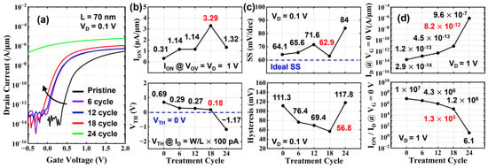
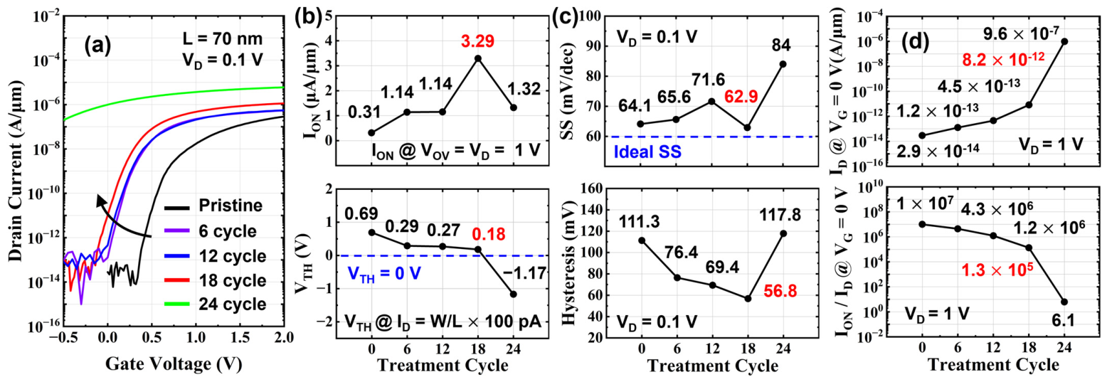
Figure 1a shows the transfer characteristics of the short-channel devices as a function of H2O treatment cycles. The pristine device exhibits typical enhancement-mode switching behavior. As the number of treatment cycles increases to 24 cycles, the device gradually becomes fully conductive and loses its switching capability. The extracted key electrical parameters from the transfer characteristics are summarized in Figure 1b–d to provide a more comprehensive evaluation of the effects of H2O treatment. As the H2O treatment cycles increase, the ON-state current (ION) gradually increases, while the VTH shifts continuously toward negative values. This behavior indicates that the H-related species introduced during H2O post-treatment tend to act as donor-like defects, contributing electrons to the conduction band [17]. Under the optimized 18-cycle condition, the device exhibits an excellent ION of 3.29 μA/μm and an optimized VTH of 0.18 V. Regarding the switching characteristics, the SS remains within the ideal range of approximately 60~70 mV/dec after 6–18 treatment cycles, reaching a near-ideal value of 62.9 mV/dec at 18 cycles. Interestingly, the hysteresis continuously decreases with increasing treatment cycles, reaching 56.8 mV at 18 cycles, corresponding to nearly a 50% reduction compared with the pristine device. It is beneficial for maintaining low-power operation. The improvements in SS and hysteresis are likely attributed to the passivation of interface defects [18]. However, when the treatment condition increases to 24 cycles, the device transitions to depletion-mode operation, and its electrical characteristics rapidly deteriorate. In particular, the static leakage current increases significantly, while the on/off current ratio decreases markedly, indicating that excessive hydrogen incorporation inevitably introduces a trade-off between performance enhancement and hydrogen-induced degradation. This degradation suggests that excessive hydrogen incorporation leads to an excess of donor-like and acceptor-like defects [31].
Figure 1.
(a) Transfer characteristics of the IGZO TFTs under different H2O treatment cycles. Dependence of (b) ION and VTH, (c) SS and hysteresis, and (d) ID @ VG = 0 V and ION/ID @ VG = 0 V on the H2O treatment cycle.
Through the ALD-based H2O post-treatment method, the amount of incorporated H-related species can be precisely controlled, allowing an optimized hydrogen incorporation window to be established at the 18-cycle condition. Under the optimized condition, the device achieves high ION, near-ideal SS, low hysteresis, acceptable static leakage current, and on/off current ratio, thereby achieving the best balance between enhanced electrical performance and hydrogen-induced degradation. Consequently, the device simultaneously exhibits fast switching, high performance, and low power, demonstrating that positive effects can still be achieved under moisture-related processing conditions.
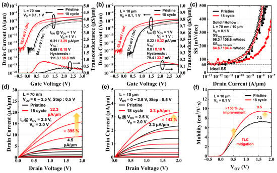
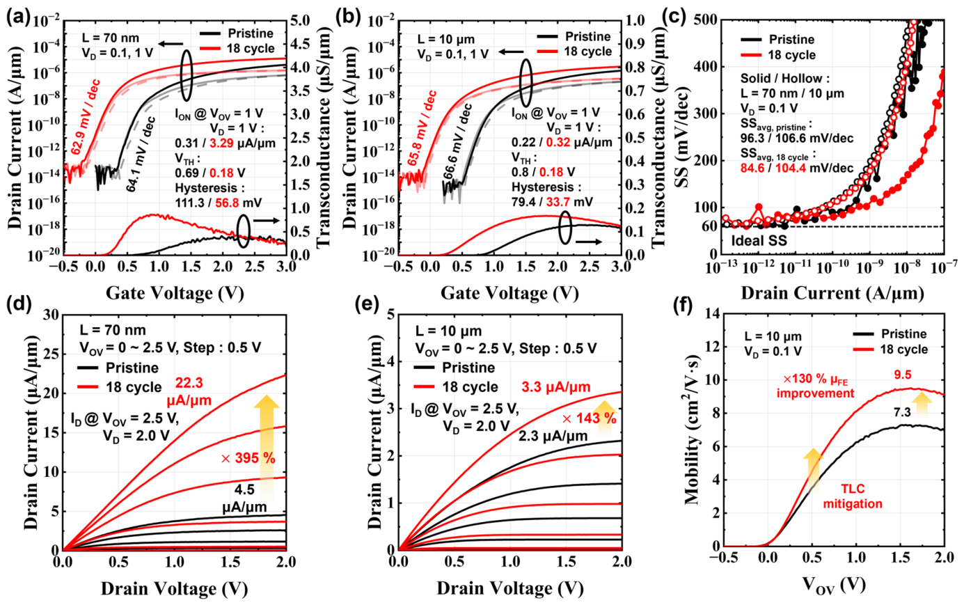
To evaluate the improvements achieved under the optimized H2O treatment condition, the electrical characteristics of both long-channel and short-channel devices are compared before and after treatment in Figure 2. The transfer characteristics shown in Figure 2a,b demonstrate that the treated devices exhibit near-ideal SS values of approximately 60 mV/dec, minimum leakage current of approximately 10−14 A/μm, VTH approaching 0 V, and significantly enhanced ION and reduced hysteresis. Figure 2c presents the SS as a function of drain current. The average subthreshold swing (SSavg) is defined as the average SS over the drain current range from 10−13 A/μm to 10−9 A/μm to evaluate switching behavior during the transition from the subthreshold to the ON-state. After H2O treatment, all devices exhibit improved SSavg values. Notably, the treated short-channel device achieves an SSavg of 84.6 mV/dec and an ION of 3.29 μA/μm at VOV = VD = 1 V. The substantial reduction in SS is attributed to the effective suppression of sub-gap defects, suggesting that the target ION can be achieved at lower supply voltages without degrading minimum leakage current, even under aggressively scaled channel lengths. In addition, the approximately tenfold increase in ION is attributed to the reduced channel resistance under aggressively scaled channel lengths, which significantly decreases the total device resistance [32]. Figure 2d,e show the output characteristics of the devices. Under VOV = 2.5 V and VD = 2 V, the treated devices exhibit significantly enhanced drive current. In particular, the short- channel device demonstrates an approximately fourfold increase in drive current, reaching 22.3 μA/μm. Figure 2f shows μFE as a function of overdrive voltage for the long-channel device. According to the carrier transport theory of oxide semiconductors [33], the mobility affected by trap-limited conduction (TLC) can be expressed as:
where μband is the band mobility, and nfree and ntrap represent the concentrations of free and trapped carriers, respectively. After H2O treatment, the introduced H-related species increase both donor-like and acceptor-like defects. Meanwhile, part of the incorporated hydrogen effectively passivates defects, thereby suppressing the influence of TLC and resulting in a steeper mobility transition behavior. However, the increase in donor-like defects is more dominant because hydrogen primarily acts as a donor, leading to an enhanced mobility of 9.5 cm2/V·s. The simultaneous achievement of steep SS, acceptable static leakage current, low-voltage operation, and high performance is not only observed in the long-channel device with L = 10 μm but also maintained in the aggressively scaled short-channel device with L = 70 nm. These results demonstrate the applicability of H2O post-treatment under extreme channel-length scaling, suggesting its compatibility with the scaling trend of front-end-of-line silicon devices for realizing BEOL-compatible integration and enabling low-power, high-density M3D integration [34,35].
μFE = μband·nfree/(nfree + ntrap)
Figure 2.
Transfer characteristics of the pristine and optimally treated devices for (a) short-channel devices and (b) long-channel devices, with the transconductance shown on the right y-axis. (c) SS as a function of drain current. Output characteristics of the pristine and treated devices for (d) short-channel devices and (e) long-channel devices. (f) Extracted μFE of the long-channel device as a function of VOV.
2.2. Analysis of Hydrogen-Related Defects
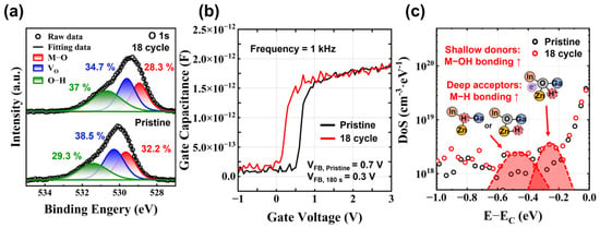
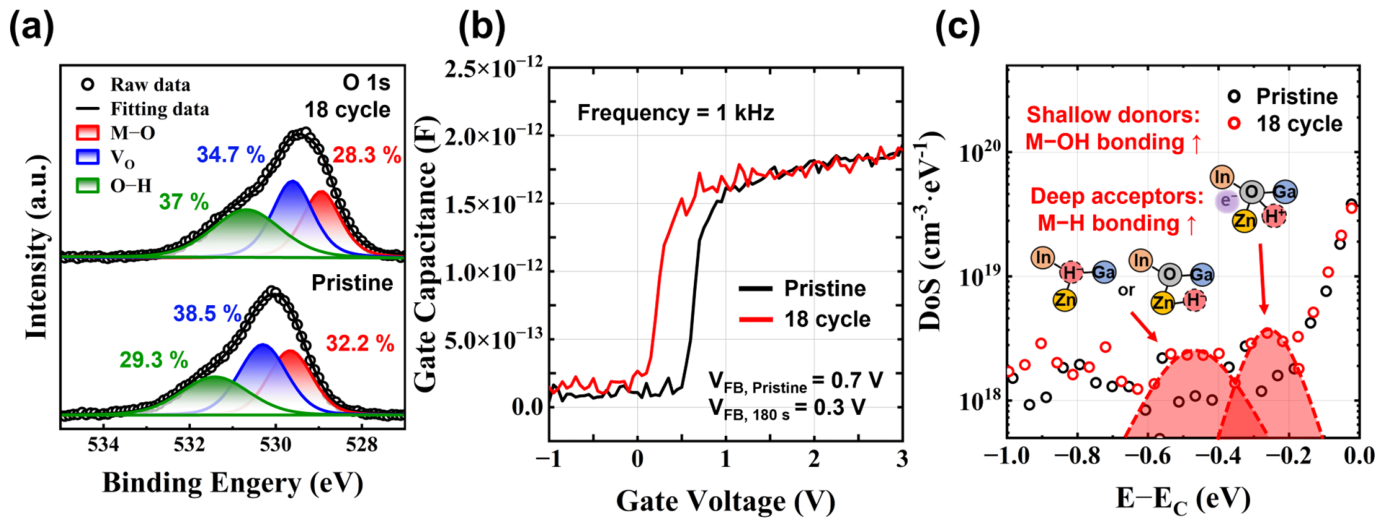
To investigate the concentration and distribution of H-related traps induced by the incorporation of H-related species into the channel after H2O treatment, XPS and capacitance–voltage (C–V) measurements were performed. The O 1s spectra before and after treatment were deconvoluted into three peaks, as shown in Figure 3a. Before treatment, the peaks corresponding to hydroxyl bonding (O–H), oxygen vacancies (VO), and M–O were located at 531.4 eV, 530.3 eV, and 529.7 eV, respectively [29]. After H2O treatment, the proportion of O–H bonding increased from 29.3% to 37%, which is consistent with hydrogen incorporation into the IGZO film. The incorporated hydrogen may contribute to donor-like behavior by releasing free electrons, consistent with the observed enhancement in mobility and the negative VTH shift. Interestingly, the concentrations of VO and M–O bonding decreased after treatment, suggesting that hydrogen incorporation may also be associated with the passivation of oxygen-related defects. This interpretation is further supported by the C–V-derived DoS analysis. Figure 3b shows the voltage-dependent gate capacitance of devices with a channel size of 10 μm × 10 μm, measured at 1 kHz before and after treatment. The negative shift in the flat-band voltage (VFB) after H2O treatment is attributed to a hydrogen-induced reduction in the IGZO semiconductor work function and/or the introduction of positively charged hydrogen-related species.
Figure 3.
(a) Deconvoluted O 1s XPS spectra before and after H2O treatment. (b) The voltage-dependent gate capacitance characteristics measured at 1 kHz for the devices before and after H2O treatment. (c) DoS distribution as a function of energy level before and after H2O treatment.
To further clarify the existence and energy distribution of hydrogen-related defects with different polarities in the channel, the sub-gap density-of-states (DoS) distribution of IGZO was extracted from low-frequency (1 kHz) C–V measurements [36], as shown in Figure 3c. The DoS distribution was extracted according to:
where q is the elementary charge, A is the channel area, TCH is the channel thickness, and COX is the maximum gate capacitance in the accumulation region. The energy level was obtained from:
After H2O treatment, two distinct Gaussian peaks were observed at EC − 0.25 eV and EC − 0.48 eV. These peaks are consistent with the energy distributions previously reported for hydrogen-related donor-like and acceptor-like defect states [37]. The corresponding reactions can be expressed as:
respectively [18,38]. Reaction (6) is accompanied by the generation of free electrons through H+ incorporation. Enhanced carrier transport, increased drive current, and a negative VTH shift are consequently observed. In reaction (7), effective passivation of oxygen VO and dangling bonds is achieved through M–H bonding. Suppression of sub-gap defects and carrier trapping behavior is therefore obtained, leading to near-ideal SS and reduced hysteresis. These results confirm that H-related defects generated after H2O treatment can simultaneously form two different polarities, thereby improving carrier transport and gate controllability. The influence of H-related defects with different polarities on the electrical characteristics after H2O treatment has therefore been clearly clarified.
H0 + O2− → [O2−H+]− + e−
H0 + VO2+ + e− → [Mx+H−]y+
2.3. Bias Stability and VTH Shift Mechanisms
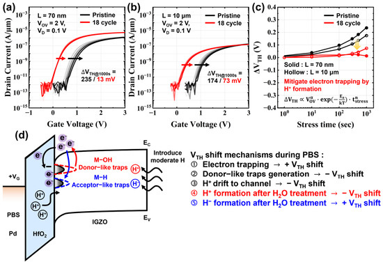
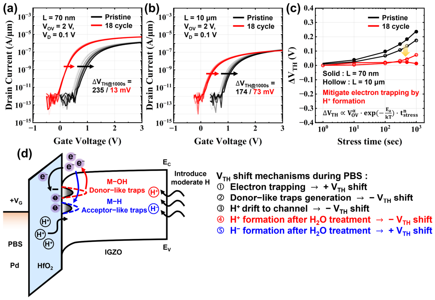
The tolerable margin for electrical variation is significantly reduced, resulting in a much narrower operating window under low-power conditions. Consequently, reliability issues become further amplified, and even a slight VTH shift may significantly affect normal circuit operation. Since the proposed H2O-treated IGZO TFTs target BEOL-compatible logic applications, reliability is evaluated using conventional PBS and negative bias stress (NBS), which is directly relevant to logic operation. In contrast, negative-bias illumination-stress is primarily used for display and optoelectronic applications, where light illumination introduces additional photo-induced degradation mechanisms [39,40]. Therefore, the influence of bias instability and the evolution mechanisms of hydrogen-related traps on VTH shift were further investigated under a fixed bias stress condition of VOV = ±2 V and VD = 0.1 V. Figure 4a,b show the dynamic evolution of the transfer characteristics of the long-channel and short-channel devices before and after H2O treatment under PBS, respectively. In contrast, the corresponding evolution of ΔVTH is summarized in Figure 4c. During PBS, three major mechanisms contribute to the VTH shift within the IGZO bulk and at the interface between the channel and gate dielectric: (1) electron trapping and (2) donor-like trap generation, where the former induces a positive VTH shift, and the latter contributes to a negative VTH shift [41]. In addition, (3) electric-field-driven H+ species can drift from the HfO2 layer into the channel, further inducing a negative VTH shift [42]. In the pristine device, the VTH instability is dominated by electron trapping, resulting in a positive ΔVTH shift. However, after ALD-based H2O treatment with an optimized amount of hydrogen incorporation and diffusion into the channel, electron trapping is effectively suppressed. This behavior is attributed to hydrogen preferentially bonding to oxygen to form H+ species, which then release electrons, thereby generating donor-like traps. The resulting negative VTH shift effectively compensates for the positive VTH shift induced by electron trapping, even though part of the incorporated hydrogen bonds with metal atoms to form H− species and generates acceptor-like traps through electron capture. The detailed PBS mechanism is schematically illustrated in Figure 4d. The ΔVTH shift was further modeled using the semi-classical power-law model for bias-temperature instability [43], and the experimental results show good agreement with the theoretical fit. Remarkably, the treated short-channel device exhibits a more balanced behavior than the long-channel device. After 1000 s of PBS, the treated short-channel device exhibits only a 13 mV ΔVTH shift, corresponding to a 94% reduction compared with the pristine device. This improvement may originate from a more uniform distribution of hydrogen-induced donor-like traps, resulting from their diffusion toward the S/D regions in the short-channel device [44].
Figure 4.
Transfer characteristics under PBS for the pristine and treated (a) short-channel devices and (b) long-channel devices. (c) Time evolution of the ΔVTH shift under PBS before and after H2O treatment. (d) Schematic illustration of the PBS mechanism.
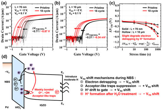
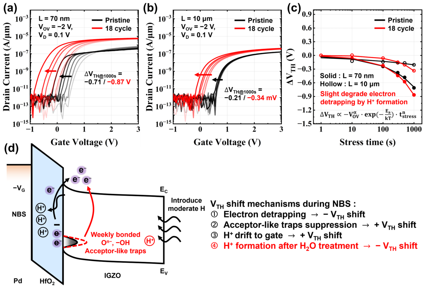
Although both short- and long-channel devices exhibit excellent PBS stability after H2O treatment, a slight degradation in stability is observed under NBS. The NBS characteristics before and after treatment are shown in Figure 5a–c. For the treated short-channel device, the ΔVTH shift slightly degrades from −0.71 V to −0.87 V after stress, while the long-channel device exhibits a similar trend. This behavior is consistent with the prediction of the semi-classical power-law model. Figure 5d illustrates the proposed mechanism of NBS-induced VTH instability. During NBS, three primary mechanisms contribute to the VTH shift: (1) electron detrapping and (2) suppression of acceptor-like traps, where the former induces a negative VTH shift, and the latter contributes to a positive VTH shift. In addition, (3) electric-field-driven H+ species drift from the channel and HfO2 layer toward the gate electrode, further contributing to a positive VTH shift [45]. In the pristine device, the VTH instability is mainly dominated by electron detrapping, resulting in a severe negative ΔVTH shift. After H2O treatment, part of the incorporated hydrogen forms O–H bonds, thereby releasing free electrons. Meanwhile, hydrogen-related acceptor-like trap states are distributed near the valence band. Under NBS, the upward band bending reduces the energy between the Fermi level and the valence band, facilitating electron de-trapping from the previously occupied hydrogen-related acceptor-like trap states near the valence band. The released electrons increase the free-electron concentration in the channel, resulting in an additional negative ΔVTH shift and consequently a slight degradation in NBS stability [20]. However, the optimized H2O treatment provides the best balance between significantly improved PBS stability and only limited degradation in NBS stability, thereby establishing an optimized hydrogen incorporation window. Since enhancement-mode devices for low-power logic applications are typically operated under PBS conditions, the improvement in PBS stability is considered more critical for practical applications.
Figure 5.
Transfer characteristics under NBS for the pristine and treated (a) short-channel devices and (b) long-channel devices. (c) Time evolution of the ΔVTH shift under NBS before and after H2O treatment. (d) Schematic illustration of the NBS mechanism.
2.4. Benchmarking of Low-Power IGZO TFTs in Performance and Reliability
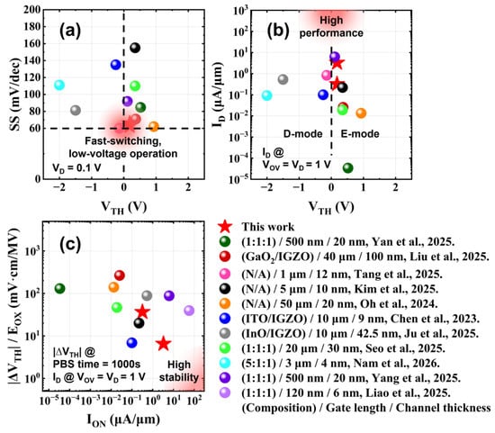
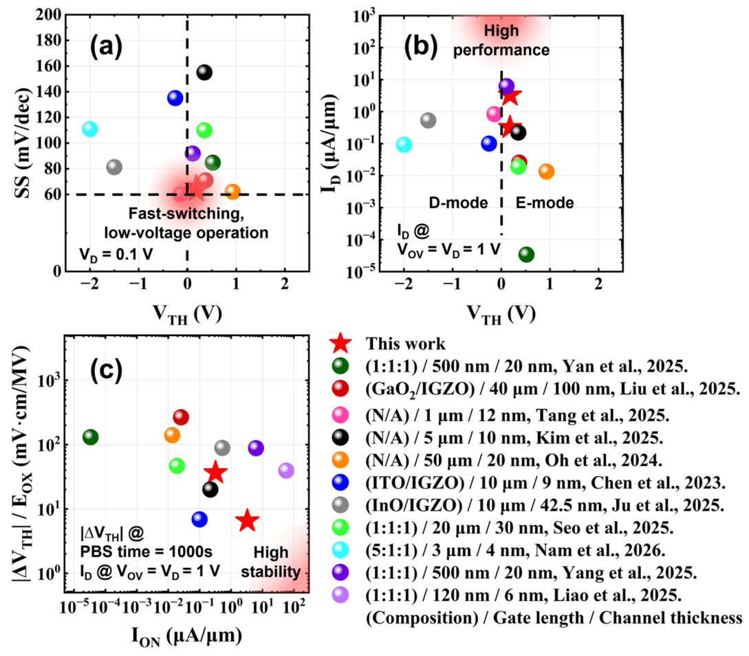
Figure 6a–c compare the key performance metrics of state-of-the-art IGZO-based devices reported in previous studies [8,9,12,14,15,16,23,29,46,47,48]. Under aggressively scaled conditions, the H2O-treated BG IGZO TFT with L = 70 nm exhibits a near-ideal SS of 62.9 mV/dec, a low VTH of 0.18 V, a high drive current of 22.3 μA/μm at VOV = VD = 1 V, and excellent PBS stability with a ΔVTH shift of only 13 mV. These results demonstrate that H2O treatment is an effective and highly competitive post-treatment approach, highlighting its potential for simultaneously achieving fast switching, low-power operation, high performance, and high reliability in scaled IGZO TFTs.
Figure 6.
Benchmark comparison of IGZO-based devices in terms of fast switching, low-power operation, high performance, and high reliability [8,9,12,14,15,16,23,29,46,47,48]: (a) SS–VTH, (b) ION–VTH, and (c) stability–ION.
3. Materials and Methods
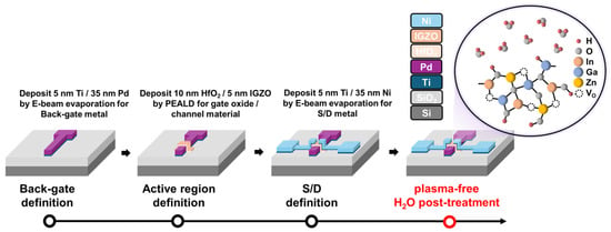
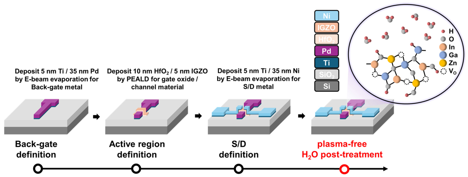
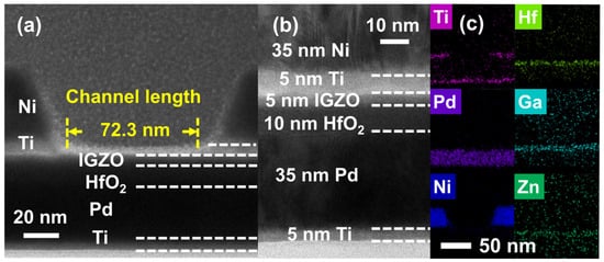
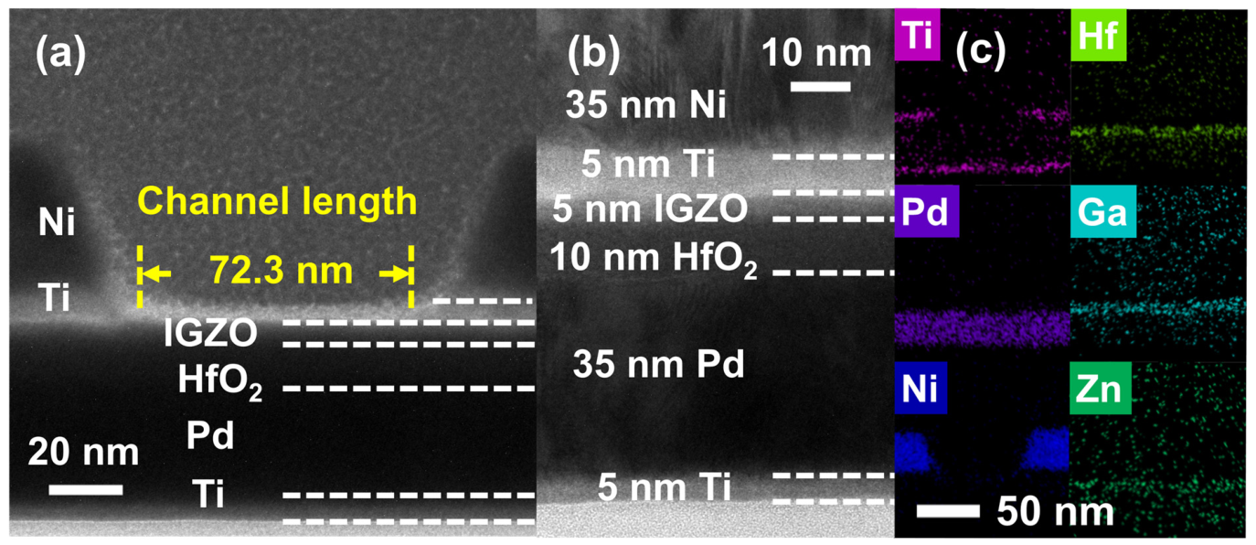
The fabrication process of the IGZO TFTs began with the deposition of a 100 nm-thick SiO2 insulating layer on an 8-inch Silicon wafer by plasma-enhanced chemical vapor deposition. After defining the back-gate (BG) region by photolithography, 5 nm Ti and 35 nm Pd were deposited by electron-beam (e-beam) evaporation and subsequently patterned by a lift-off process to form the BG electrode. Subsequently, 10 nm HfO2 and 5 nm IGZO were sequentially deposited by plasma-enhanced atomic layer deposition (PEALD) as the gate dielectric and channel layer, respectively. For HfO2 deposition, TMAHf and H2O were used as the precursor and oxidant, respectively. The IGZO channel with an In:Ga:Zn ratio of 1:1:1 was deposited using oxygen plasma as the oxidant. The deposition temperature was maintained at 250 °C throughout the PEALD process. The active region was then defined by photolithography followed by Ar plasma etching. After source/drain (S/D) pattern definition, 5 nm Ti and 35 nm Ni were deposited by e-beam evaporation and patterned by lift-off to form the S/D contacts. Photolithography, combined with dry and wet etching, was further used to expose the BG electrode. Finally, plasma-free H2O post-treatment was performed in the PEALD chamber at 250 °C and 0.048 Torr. on BG IGZO TFTs with a channel width (W) of 1 μm, channel lengths (L) of 70 nm and 10 μm, and a gate-to-S/D overlap length of 0.5 μm on both S/D sides. The devices were treated with 6, 12, 18, and 24 H2O cycles to introduce hydrogen-related species into the IGZO channel and improve the device performance. Each H2O pulse had a pulse width of 0.06 s, followed by a 5 s N2 purge. Devices with L = 70 nm and 10 μm were used as representative short-channel and long-channel devices, respectively. The detailed fabrication flow is illustrated in Figure 7. To minimize device-to-device variation, the same device was characterized before and after H2O treatment. Figure 8a,b show cross-sectional transmission electron microscopy (TEM) images of the BG IGZO TFT, clearly demonstrating the 70 nm channel length and well-defined layer structure. Figure 8c presents the energy-dispersive spectroscopy (EDS) mapping results, confirming the elemental distributions of Ti, Pd, Ni, Hf, Ga, and Zn. The VTH was extracted using the constant-current method with ID = (W/L) × 100 pA for short-channel devices and ID = (W/L) × 1 nA for long-channel devices to obtain an appropriate VTH extraction criterion under aggressive scaling conditions. The field-effect mobility (μFE) was extracted from the maximum transconductance under low drain voltage (VD) conditions according to:
where COX and gm represent the gate oxide capacitance per unit area and transconductance, respectively. The overdrive voltage (VOV) was defined as VOV = VG − VTH. For the X-ray photoelectron spectroscopy (XPS) samples, HfO2 was intentionally omitted to avoid the overlap between the Hf 4f and In 3d binding energy peaks, which could interfere with the chemical bonding analysis [49].
μFE = L·gm/(W·COX·VD)
Figure 7.
The fabrication process flow of the BG IGZO TFTs.
Figure 8.
(a) Cross-sectional TEM image of the channel region in the BG IGZO TFTs. (b) Magnified TEM image of the S/D side region. (c) EDS mapping results.
4. Conclusions
In this work, an ALD-based plasma-free H2O treatment method is proposed to effectively modulate H-related defects in IGZO thin-film TFTs through controllable hydrogen incorporation, and its applicability to aggressively scaled short-channel devices is successfully demonstrated. After optimization, the IGZO TFT with a channel length of 70 nm simultaneously exhibits a near-ideal SS, low VTH, acceptable static leakage current, high drive capability, and excellent PBS stability. Through XPS and DoS analyses, this work further reveals donor-like and acceptor-like defects induced by hydrogen-related traps. It clarifies their influence on carrier transport, gate controllability, bias stability, and the mechanisms responsible for VTH shift. These improvements are attributed to the formation of H-related traps with two different polarities after H2O treatment. Hydrogen primarily acts as a shallow donor, providing free electrons and thereby enhancing carrier transport. Meanwhile, another portion of hydrogen passivates oxygen vacancies and dangling bonds through the formation of M–H bonds, thereby suppressing electron trapping. These results demonstrate that controllable hydrogen incorporation achieves the best balance between enhanced electrical performance and hydrogen-induced degradation, enabling scaled IGZO TFTs with low-power operation, high performance, and high reliability, providing a viable pathway toward future high-density BEOL-compatible electronics and M3D integrated applications.
Author Contributions
K.-T.H., Y.-C.W. and F.-J.H. conceived and designed the experiments. Y.-W.F., J.-Y.L., C.-L.C., Y.-C.Y., Y.-C.O. and L.-C.L. participated in device fabrication and electrical measurements. K.-T.H. and Y.-W.F. performed and participated in the data analysis. G.-L.L. and Y.-H.L. provided critical suggestions. K.-T.H., Y.-C.W. and F.-J.H. co-wrote the manuscript, and all authors contributed to its final version. All authors have read and agreed to the published version of the manuscript.
Funding
This work was supported in part by the National Science and Technology Council, Taiwan, under NSTC 115-2221-E-007-139-MBK and NSTC 114-2221-E-492-022, and in part by Taiwan Semiconductor Research Institute (TSRI), National Institutes of Applied Research, Taiwan.
Data Availability Statement
The original contributions presented in this study are included in the article. Further inquiries can be directed to the corresponding authors.
Acknowledgments
The authors are grateful for the support of the United Microelectronics Corporation (UMC) Fellowship.
Conflicts of Interest
The authors declare no conflicts of interest.
Abbreviations
The following abbreviations are used in this manuscript:
| PDynamic | Dynamic power consumption |
| PStatic | Static power consumption |
| M3D | Monolithic three-dimensional |
| AOSs | Amorphous oxide semiconductors |
| IGZO | Indium gallium zinc oxide |
| TFTs | Thin-film transistors |
| VTH | Threshold voltage |
| SS | Subthreshold swing |
| PBS | Positive bias stress |
| H-related | hydrogen-related |
| M–O | Metal–oxygen bonding |
| ALD | Atomic layer deposition |
| BEOL | Back-end-of-line |
| BG | Back-gate |
| e-beam | Electron-beam |
| PEALD | Plasma-enhanced atomic layer deposition |
| S/D | Source/drain |
| W | Channel width |
| L | Channel length |
| TEM | Transmission electron microscopy |
| EDS | Energy-dispersive spectroscopy |
| μFE | Field-effect mobility |
| VD | Drain voltage |
| VOV | Drive voltage |
| XPS | X-ray photoelectron spectroscopy |
| ION | ON-state current |
| IOFF | Leakage current |
| SSavg | Average subthreshold swing |
| TLC | Trap-limited conduction |
| C–V | Capacitance–voltage |
| O–H | Hydroxyl bonding |
| VO | Oxygen vacancies |
| VFB | Flat-band voltage |
| Dit | Interface trap density |
| DoS | Density-of-states |
| NBS | Negative bias stress |
References
- Gao, P.; Adnan, M. Overview of emerging electronics technologies for artificial intelligence: A review. Mater. Today Electron. 2025, 11, 100136. [Google Scholar] [CrossRef] [Scilit]
- Jain, S.; Li, S.; Zheng, H.; Li, L.; Fong, X.; Ang, K.-W. Heterogeneous integration of 2D memristor arrays and silicon selectors for compute-in-memory hardware in convolutional neural networks. Nat. Commun. 2025, 16, 2719. [Google Scholar] [CrossRef] [Scilit] [PubMed]
- Ren, S.; Huang, Q.; Li, D.; Wang, S.; Chen, Y.; Ren, H.; Wang, Y.; Tang, Y.; Zhu, B. Oxide Semiconductor Thin-Film Transistors for Low-Power Electronics. Adv. Sci. 2026, 13, e22487. [Google Scholar] [CrossRef] [Scilit] [PubMed]
- Charnas, A.; Zhang, Z.; Lin, Z.; Zheng, D.; Zhang, J.; Si, M.; Ye, P.D. Review—Extremely Thin Amorphous Indium Oxide Transistors. Adv. Mater. 2024, 36, 2304044. [Google Scholar] [CrossRef] [Scilit] [PubMed]
- Datta, S.; Sarkar, E.; Aabrar, K.; Deng, S.; Shin, J.; Raychowdhury, A.; Yu, S.; Khan, A. Amorphous Oxide Semiconductors for Monolithic 3D Integrated Circuits. In Proceedings of the 2024 IEEE Symposium on VLSI Technology and Circuits (VLSI Technology and Circuits), Honolulu, HI, USA, 16–20 June 2024; pp. 1–2. [Google Scholar]
- Kim, H.-M.; Kim, D.-G.; Kim, Y.-S.; Kim, M.; Park, J.-S. Atomic layer deposition for nanoscale oxide semiconductor thin film transistors: Review and outlook. Int. J. Extrem. Manuf. 2023, 5, 012006. [Google Scholar] [CrossRef] [Scilit]
- Kim, J.Y.; Kim, H.; Kim, D.; Jang, H.W. Advancements of Amorphous IGZO-Based Transistors: Materials, Processing, and Devices. ACS Appl. Electron. Mater. 2025, 7, 4703–4728. [Google Scholar] [CrossRef] [Scilit]
- Yan, G.; Yang, Y.; Tai, L.; Chen, Y.; Ma, X.; Xiang, J.; Xu, G.; Wang, G.; Yin, H.; Zhao, C. Linear Tuning of Positive Threshold Voltage in IGZO Thin-Film Transistors via Gate Dielectric Stack Engineering. IEEE Electron Device Lett. 2025, 46, 781–784. [Google Scholar] [CrossRef] [Scilit]
- Liu, Z.C.; Xia, Y.H.; Li, J.C.; Zheng, Y.H.; Qi, S.M.; Dai, D.; Yang, H.X.; Zhang, Y.Y.; Ma, Y.X.; Wang, Y.L. High-k Gated Ga2O3/IGZO Heterostructure TFTs With 70.9 mV/dec Subthreshold Swing Fabricated at a Low Thermal Budget of 200 °C. IEEE Electron Device Lett. 2025, 46, 1793–1796. [Google Scholar] [CrossRef] [Scilit]
- Seong, S.; Ha, T.; Jung, S.; Jeong, W.; Chung, Y. Recent Progress and Opportunities in Oxide Semiconductor Devices for In-Memory and Neuromorphic Computing. Adv. Electron. Mater. 2026, 12, e00521. [Google Scholar] [CrossRef] [Scilit]
- Chung, S.W.; Yoon, S.H.; Jeong, J.K. Oxide semiconductor gain cell-embedded memory: Materials and integration strategies for next generation on-chip memory. Commun. Eng. 2026, 5, 39. [Google Scholar] [CrossRef] [Scilit] [PubMed]
- Tang, H.; Lin, D.; Subhechha, S.; Chasin, A.; Matsubayashi, D.; Setten, M.v.; Wan, Y.; Dekkers, H.; Li, J.; Subramanian, S.; et al. The Impact of Process Steps on Nearly Ideal Subthreshold Slope in 300-mm Compatible InGaZnO TFTs. IEEE Electron Device Lett. 2025, 46, 761–764. [Google Scholar] [CrossRef] [Scilit]
- Zhang, J.; Zhang, Z.; Lin, Z.; Xu, K.; Dou, H.; Yang, B.; Zhang, X.; Wang, H.; Ye, P.D. First Demonstration of BEOL-Compatible Atomic-Layer-Deposited InGaZnO TFTs with 1.5 nm Channel Thickness and 60 nm Channel Length Achieving ON/OFF Ratio Exceeding 1011, SS of 68 mV/dec, Normal-off Operation and High Positive Gate Bias Stability. In Proceedings of the 2023 IEEE Symposium on VLSI Technology and Circuits (VLSI Technology and Circuits), Kyoto, Japan, 11–16 June 2023; pp. 1–2. [Google Scholar]
- Kim, H.; Park, S.; Jeong, J.; Cha, J.H.; Lee, H.; Sung, C.; Na, J.; Heo, K.; Cho, S.H.; Choi, S.Y.; et al. Millisecond Pulsed Light Annealing for Improving Performance of Top-Gate Self-Aligned a-IGZO TFT. IEEE Trans. Electron Devices 2025, 72, 2399–2405. [Google Scholar] [CrossRef] [Scilit]
- Oh, S.H.; Lee, C.H.; Kim, H.T.; Park, J.I.; Kim, M.J.; Park, S.J.; Im, S.G.; Cho, S.H.; Cho, B.J. Overcoming Performance Limitation of IGZO FET by iCVD Fluorine Doping. In Proceedings of the 2024 IEEE Symposium on VLSI Technology and Circuits (VLSI Technology and Circuits), Honolulu, HI, USA, 16–20 June 2024; pp. 1–2. [Google Scholar]
- Chen, C.K.; Xu, Z.; Hooda, S.; Pan, J.; Zamburg, E.; Thean, A.V.Y. Negative-U Defect Passivation in Oxide-Semiconductor by Channel Defect Self-Compensation Effect to Achieve Low Bias Stress VTH Instability of Low-Thermal Budget IGZO TFT and FeFETs. In Proceedings of the 2023 International Electron Devices Meeting (IEDM), San Francisco, CA, USA, 9–13 December 2023; pp. 1–4. [Google Scholar]
- Jang, J.T.; Ko, D.; Choi, S.J.; Kim, D.M.; Kim, D.H. Observation of Hydrogen-Related Defect in Subgap Density of States and Its Effects Under Positive Bias Stress in Amorphous InGaZnO TFT. IEEE Electron Device Lett. 2021, 42, 708–711. [Google Scholar] [CrossRef] [Scilit]
- Oh, S.; Kim, H.; Oh, J.; Kim, H.; Kim, S.; Cho, H.-S.; Kim, C. Enhancing proton irradiation tolerance of a-IGZO thin-film transistors through hydrogen doping. J. Mater. Chem. C 2026, 14, 3637–3647. [Google Scholar] [CrossRef] [Scilit]
- Mattson, G.W.; Vogt, K.T.; Wager, J.F.; Graham, M.W. Hydrogen incorporation into amorphous indium gallium zinc oxide thin-film transistors. J. Appl. Phys. 2022, 131, 105701. [Google Scholar] [CrossRef] [Scilit]
- Yang, J.; Liao, P.-Y.; Chang, T.-C.; Chiang, H.-C.; Chen, B.-W.; Chien, Y.-C.; Lin, D.; Ren, J.; Fu, R.; Qu, M.; et al. H2O adsorption on amorphous In-Ga-Zn-O thin-film transistors under negative bias stress. Appl. Phys. Lett. 2017, 111, 073506. [Google Scholar] [CrossRef] [Scilit]
- Li, G.; Abliz, A.; Xu, L.; André, N.; Liu, X.; Zeng, Y.; Flandre, D.; Liao, L. Understanding hydrogen and nitrogen doping on active defects in amorphous In-Ga-Zn-O thin film transistors. Appl. Phys. Lett. 2018, 112, 253504. [Google Scholar] [CrossRef] [Scilit]
- Chien, Y.C.; Chang, T.C.; Chiang, H.C.; Chen, H.M.; Tsao, Y.C.; Shih, C.C.; Chen, B.W.; Liao, P.Y.; Chu, T.Y.; Yang, Y.C.; et al. Role of H2O Molecules in Passivation Layer of a-InGaZnO Thin Film Transistors. IEEE Electron Device Lett. 2017, 38, 469–472. [Google Scholar] [CrossRef] [Scilit]
- Ju, S.; Li, J.; Tang, Y.; Qian, W.; Zhang, F.; Zhu, J.; Tian, X.; Yang, S.; Zhang, L.; Lu, L.; et al. Stabilizing ALD Ultrathin In2O3 TFTs Under High Humidity Ambient by an Added IGZO Layer. IEEE Electron Device Lett. 2025, 46, 773–776. [Google Scholar] [CrossRef] [Scilit]
- Fan, J.Y.; Jiang, Z.D.; Liu, J.W.; Liu, M.R.; Zhang, Y.H.; Yang, S.J.; Lv, Z.H.; Zheng, X.; Li, J.X.; Li, Q.; et al. Hydrogenation-Immune Oxide Semiconductor FETs via Hetero-Integration-Compatible Hydrogen Evacuation Layer. In Proceedings of the 2025 IEEE International Electron Devices Meeting (IEDM), San Francisco, CA, USA, 6–10 December 2025; pp. 1–4. [Google Scholar]
- Kuo, Y.H.; Zhang, C.; Ravikumar, P.G.; Kang, S.; Song, T.; Villena, M.A.; Larcher, L.; Kim, H.; Hong, M.; Yun, P.; et al. Experiments and Modeling of Defect Dynamics and BTI in Doped In2O3 TFTs Undergoing Densification during 400 °C Post-BEOL Forming Gas Annealing (FGA). In Proceedings of the 2025 IEEE International Electron Devices Meeting (IEDM), San Francisco, CA, USA, 6–10 December 2025; pp. 1–4. [Google Scholar]
- Kim, G.B.; Kim, T.; Bak, J.; Choi, C.H.; Chung, S.W.; Kang, Y.; Jeong, J.K. Beneficial Hydrogen Doping in Single Spinel Phase Crystallized IZTO Thin-Film Transistors. IEEE Electron Device Lett. 2024, 45, 1831–1834. [Google Scholar] [CrossRef] [Scilit]
- Li, T.; Liu, X.; Ren, J.; Hu, P.; Qian, Y.; Jin, T.; Sun, J.; Chen, Z.; Liang, L.; Cao, H. High-mobility InSnZnO Thin Film Transistors via Introducing Water Vapor Sputtering Gas. ACS Appl. Mater. Interfaces 2024, 16, 31237–31246. [Google Scholar] [CrossRef] [Scilit] [PubMed]
- Ding, Y.; Ren, Y.; Zhang, D.; Liu, G.; Shan, F. Water- and DUV-induced self-passivation for In2O3 nanofiber field effect transistor. Appl. Phys. Lett. 2022, 121, 033301. [Google Scholar] [CrossRef] [Scilit]
- Seo, T.; Yun, J.; Kim, S.-M.; Jin, C.; Park, S.; Seong, S.; Kang, D.H.; Lee, B.H.; Chung, Y. Hydrogen Plasma Treatment for Improving Reliability of In-Ga-Zn-O Transistors Without Side Effects Through Post-Annealing Process. Adv. Electron. Mater. 2025, 11, 2400893. [Google Scholar] [CrossRef] [Scilit]
- Zhang, J.; Wang, Y.; Chai, Z.; Zhao, D.; Lu, X. Six-Fold Mobility Improvement for All-Solution-Processed Metal Oxide Thin Film Transistors Via a Controlled Humidity Annealing Process. Adv. Funct. Mater. 2025, 35, 2507594. [Google Scholar] [CrossRef] [Scilit]
- Park, J.-S.; Jeong, J.K.; Chung, H.-J.; Mo, Y.-G.; Kim, H.D. Electronic transport properties of amorphous indium-gallium-zinc oxide semiconductor upon exposure to water. Appl. Phys. Lett. 2008, 92, 072104. [Google Scholar] [CrossRef] [Scilit]
- Tang, H.; Dekkers, H.; Rassoul, N.; Sutar, S.; Subhechha, S.; Afanas’ev, V.; Houdt, J.V.; Delhougne, R.; Kar, G.S.; Belmonte, A. Study of Contact Resistance Components in Short-Channel Indium-Gallium-Zinc-Oxide Transistor. IEEE Trans. Electron Devices 2024, 71, 567–573. [Google Scholar] [CrossRef] [Scilit]
- Lee, S.; Ghaffarzadeh, K.; Nathan, A.; Robertson, J.; Jeon, S.; Kim, C.; Song, I.H.; Chung, U.I. Trap-limited and percolation conduction mechanisms in amorphous oxide semiconductor thin film transistors. Appl. Phys. Lett. 2011, 98, 203508. [Google Scholar] [CrossRef] [Scilit]
- Jana, K.; Kang, J.; Liu, S.; Athena, F.F.; Huang, C.H.; Tang, Y.; Chen, H.J.Y.; Saini, B.; Hartanto, J.; Bennett, R.K.A.; et al. Key to Low Supply Voltage: Transition Region of Oxide Semiconductor Transistors. In Proceedings of the 2025 Symposium on VLSI Technology and Circuits (VLSI Technology and Circuits), Kyoto, Japan, 8–12 June 2025; pp. 1–3. [Google Scholar]
- Sun, C.; Yi, T.; Shi, X.; Duan, R.; Dong, J.; Wang, Z.; Zhou, Z.; Zhao, Y.; Zhao, K.; Han, D.; et al. BEOL-Compatible ITO/ZnO Transistors with Record-Small Transition Region Width of 80 mV and Ultra-High Mobility of 150 cm2V−1s−1. In Proceedings of the 2025 IEEE International Electron Devices Meeting (IEDM), San Francisco, CA, USA, 6–10 December 2025; pp. 1–4. [Google Scholar]
- Wang, W.; Wang, P.; Dai, M. Simplification of sub-gap density of states extraction method for amorphous In-Ga-Zn-O thin-film transistors by a single capacitance-voltage curve. Microelectron. Reliab. 2018, 83, 111–114. [Google Scholar] [CrossRef] [Scilit]
- Ide, K.; Nomura, K.; Hosono, H.; Kamiya, T. Electronic Defects in Amorphous Oxide Semiconductors: A Review. Phys. Status Solidi (A) 2019, 216, 1800372. [Google Scholar] [CrossRef] [Scilit]
- Fathi, M.; Mamun, M.A.A.; Rodriguez-Davila, R.A.; Alam, S.; Kim, J.; Pantha, T.H.; Pesic, M.; Quevedo-Lopez, M.; Cho, K.; Dutta, S.; et al. Investigation of the Impact of Hydrogen Defects on the VT shift in Back-Gate IGZO TFTs. In Proceedings of the 2025 IEEE International Reliability Physics Symposium (IRPS), Monterey, CA, USA, 30 March–3 April 2025; pp. 1–5. [Google Scholar]
- de Jamblinne de Meux, A.; Pourtois, G.; Genoe, J.; Heremans, P. Effects of hole self-trapping by polarons on transport and negative bias illumination stress in amorphous-IGZO. J. Appl. Phys. 2017, 123, 161513. [Google Scholar] [CrossRef] [Scilit]
- Kim, H.J.; Park, S.Y.; Jung, H.Y.; Son, B.G.; Lee, C.-K.; Lee, C.-K.; Jeong, J.H.; Mo, Y.-G.; Son, K.S.; Ryu, M.K.; et al. Role of incorporated hydrogen on performance and photo-bias instability of indium gallium zinc oxide thin film transistors. J. Phys. D Appl. Phys. 2013, 46, 055104. [Google Scholar] [CrossRef] [Scilit]
- Lin, J.Y.; Zhang, Z.; Lin, Z.; Niu, C.; Zhang, Y.; Zhang, Y.; Kim, T.; Jang, H.; Sung, C.; Hong, M.; et al. First Demonstration of Top-Gate Enhancement- Mode ALD In2O3 FETs With High Thermal Budget of 600 °C for DRAM Applications. IEEE Electron Device Lett. 2024, 45, 1851–1854. [Google Scholar] [CrossRef] [Scilit]
- Kong, Q.; Liu, G.; Sun, C.; Zhang, D.; Jiao, L.; Wang, Y.; Nguyen, B.Y.; Gong, X. Beyond ΔVth: Unlock New Insights into Hydrogen-Induced BTI in ITO FETs through Gm and RC Dynamics. In Proceedings of the 2025 IEEE International Electron Devices Meeting (IEDM), San Francisco, CA, USA, 6–10 December 2025; pp. 1–4. [Google Scholar]
- Aabrar, K.A.; Kirtania, S.G.; Deng, S.; Choe, G.; Khan, A.; Yu, S.; Datta, S. Improved Reliability and Enhanced Performance in BEOL Compatible W-doped In2O3 Dual-Gate Transistor. In Proceedings of the 2023 International Electron Devices Meeting (IEDM), San Francisco, CA, USA, 9–13 December 2023; pp. 1–4. [Google Scholar]
- Liu, G.; Kong, Q.; Zhang, D.; Wang, X.; Zhou, Z.; Jiao, L.; Han, K.; Kang, Y.; Nguyen, B.Y.; Ni, K.; et al. Hydrogen-Related Instability of IGZO Field-Effect Transistors. IEEE Trans. Electron Devices 2024, 71, 2995–3001. [Google Scholar] [CrossRef] [Scilit]
- Sarkar, E.; Zhang, C.; Chakraborty, D.; Kirtania, S.G.; Aabrar, K.A.; Park, H.; Shin, J.; Lee, H.J.; Tian, M.; Khan, A.I.; et al. First Demonstration of High-Performance and Extremely Stable W-Doped In2O3 Gate-All-Around (GAA) Nanosheet FET. IEEE Trans. Electron Devices 2025, 72, 2662–2669. [Google Scholar] [CrossRef] [Scilit]
- Nam, K.; Niu, C.; Jang, H.; Park, B.; Park, Y.; Lee, Y.; Alam, M.A.; Jeong, C.; Ye, P.D. Characterization of Thermal Stability and Unexpected Mobility Enhancement in IGZO FETs Measured Up to 750 °C. IEEE Electron Device Lett. 2026, 47, 542–545. [Google Scholar] [CrossRef] [Scilit]
- Yang, Y.; Yan, G.; Luo, J.; Lu, Y.; Bao, Y.; Niu, C.; Ma, X.; Xiang, J.; Xu, G.; Wang, G.; et al. Unveiling the Unique Region Dependence of Bias Stability in Sub-μm IGZO TFTs Using Floating Channel Effect for 3D DRAM. IEEE Electron Device Lett. 2025, 46, 290–293. [Google Scholar] [CrossRef] [Scilit]
- Liao, F.; Zhu, Z.; Li, Z.; Yang, G.; Liu, M.; Chen, K.; Lu, W.; Wu, Z.; Zhang, X.; Mao, N.; et al. High-density three-dimensional integration of dynamic random-access memory using vertical dual-gate IGZO TFTs. Nat. Commun. 2025, 16, 10932. [Google Scholar] [CrossRef] [Scilit] [PubMed]
- Yu, T.-Y.; Jan, W.-S.; Wu, Y.S.; Lin, K.-L.; Chou, T.-H. Band energy and electronic behavior of HfO2 on In2O3 thin films enhanced by oxygen annealing. J. Appl. Phys. 2025, 138, 145302. [Google Scholar] [CrossRef] [Scilit]
Disclaimer/Publisher’s Note: The statements, opinions and data contained in all publications are solely those of the individual author(s) and contributor(s) and not of MDPI and/or the editor(s). MDPI and/or the editor(s) disclaim responsibility for any injury to people or property resulting from any ideas, methods, instructions or products referred to in the content. |
© 2026 by the authors. Licensee MDPI, Basel, Switzerland. This article is an open access article distributed under the terms and conditions of the Creative Commons Attribution (CC BY) license.