


Abstract
Ferrite is an essential functional material for high-power nonreciprocal microwave components, such as circulators and isolators, and its secondary electron emission (SEE) property is critical for suppressing the multipactor effect under vacuum conditions. In this work, we propose a surface engineering strategy based on periodic raised microstructures to regulate the secondary electron yield (SEY) of ferrite coatings/substrates. A Monte Carlo-based numerical method is developed to calculate the SEY of ferrite with hexagonal and annular microprotrusions of varying heights and geometric parameters. The dependence of SEY on microstructure dimensions is systematically analyzed. Spinel ferrite samples with designed microstructures are fabricated via mechanical processing. For hexagonal column arrays with a height of 1.5 mm, a side length of 0.5 mm, and a pitch of 1.67 mm, the maximum SEY is reduced from 2.4 (smooth surface) to 1.7 while the annular concentric protrusion arrays decrease the maximum SEY to 2.1. Effective suppression is achieved over the entire incident energy range for both microstructural designs. Despite a lower reduction, the annular arrays offer geometrically isotropic electron trapping, which may be advantageous for devices with circular or coaxial cavity geometries where directional dependence of the surface texture is undesirable. The results demonstrate that tailored surface microstructures can significantly mitigate SEE of ferrite, providing a promising route for developing high-performance ferrite coatings toward multipactor suppression in space microwave devices.
1. Introduction
Secondary electron multiplication, also known as multipactor, refers to a vacuum-triggered electron avalanche effect [1,2,3,4]. As a typical high-power vacuum radio frequency (RF) breakdown phenomenon peculiar to microwave vacuum devices, it can further induce low-pressure discharge, surface flashover and plasma discharge under high-vacuum operating environments. These cascaded discharge effects will continuously erode the internal structure of devices, trigger local ablation and dielectric breakdown, and severely degrade the power endurance, transmission efficiency and operational stability of microwave components, ultimately inflicting irreversible damage to the long-term reliable operation of spacecraft payloads, particle accelerators and various vacuum electronic systems [5,6,7]. Under high-power radio frequency (RF) fields, stray free electrons existing in vacuum gaps are accelerated periodically by the alternating RF electric field. These high-speed electrons collide violently with the metal or dielectric material surfaces of microwave components and induce secondary electron emission (SEE) [8]. The intensity of secondary electron emission is quantitatively characterized by the secondary electron yield (SEY), which represents the average number of secondary electrons excited by a single incident primary electron. If SEY exceeds unity, the number of electrons in the vacuum gap will increase exponentially with successive collisions, and continuous electron multiplication and avalanche development can be formed. This uncontrolled electron avalanche behavior will further trigger severe RF breakdown, microwave power loss, thermal accumulation and irreversible surface material degradation, seriously restricting the high-power bearing capacity and service life of vacuum microwave devices [9]. Therefore, suppressing the generation and development of SEE and reducing the maximum SEY of component material surfaces to below the critical threshold are the core and essential technical approaches for effective multipactor mitigation and high-power performance improvement of vacuum RF devices.
Ferrite materials, particularly spinel-structured ferrites, possess excellent electromagnetic characteristics, including favorable magnetic permeability, low dielectric loss, and stable microwave transmission performance. Owing to these unique magnetic and dielectric properties, they have become indispensable functional materials and are widely adopted in high-power nonreciprocal microwave devices such as circulators and isolators. For spaceborne ferrite microwave components operating in low-orbit or geostationary orbit environments, high-vacuum conditions together with long-term high-power RF operating states elevate the probability of multipactor occurrence [10]. In comparison with common structural metals and traditional low-loss dielectric materials widely used in vacuum microwave systems, ferrite materials inherently exhibit a relatively higher maximum SEY. Such prominent SEE features easily trigger continuous electron avalanche multiplication under high-power RF fields [11]. Consequently, the high SEY property of ferrites has become a critical technical bottleneck restricting the high-power bearing capability, operational reliability, and service life of space nonreciprocal microwave components, severely limiting their engineering promotion and high-power application prospects.
Surface modification and coating engineering have been widely adopted to tailor surface electronic properties and suppress SEE of materials [11,12,13,14]. Typical strategies include TiN coatings [15,16], laser ablations [17,18,19,20], and chemical etching [21]. Among these, periodic micro/nanostructures have attracted increasing attention because they can trap secondary electrons and reduce effective SEY without introducing additional materials or compromising bulk properties. For ferrite, however, the development of robust, easily fabricated, and scalable surface structures for ferrite SEE regulation remains challenging.
To contextualize the novelty of our approach, quantitative benchmarking against established SEY suppression techniques is essential. TiN coatings, widely used in accelerators, reduce the peak SEY of stainless steel from ~2.5 to below 2 [15], but on ferrite kickers, they exhibit limited suppression efficiency and introduce eddy current heating and field diffusion issues in fast-pulsed systems [15,16]. Laser ablation methods, particularly Laser-Engineered Surface Structures (LESSs) [17,18], achieve remarkable SEY reduction on Ni/Zn ferrites (from 2.1 to 0.81) [19], yet they require expensive ultrafast UV laser systems, offer low processing speeds, and involve complex parameter optimization that hinders large-scale, cost-effective fabrication. Chemical etching, while effective for metals like silver (yielding a 45% reduction) [21], is fundamentally incompatible with the chemically inert spinel ferrite structure. These comparative analyses are summarized in Table 1.
Table 1.
Quantitative comparison of mainstream ferrite SEY suppression technologies.
It is also worth noting that while advanced techniques such as ultrafast laser ablation or additive manufacturing may offer higher feature resolution in principle, their application to spinel ferrites is currently constrained by thermal damage, interfacial defects, low throughput, and high cost, making them less practical for scalable engineering implementation on planar ferrite substrates. Nevertheless, these approaches remain of interest as potential future routes for further structural optimization once the associated processing challenges are adequately addressed.
In our previous work, we demonstrated that dense microscale textures can reduce ferrite SEY and suppress multipactor in ferrite circulators. To further enhance structural stability and mechanical robustness, we propose in this study periodic raised microstructures directly fabricated on spinel ferrite surfaces. Hexagonal and annular microprotrusions are designed and optimized via Monte Carlo simulation. The probabilistic Monte Carlo framework for simulating SEE phenomena has been extensively developed in the accelerator physics community, notably by Furman and Pivi for electron-cloud studies, while foundational investigations by Bronshtein and Fraiman established key empirical regularities in SEY behavior across elemental solids. More recently, Cimino et al. have provided critical insights into the low-energy SEY regime, which is particularly relevant to multipactor initiation. Our simulation approach builds upon these established principles while focusing specifically on the geometric trapping effects of raised microstructures on ferrite surfaces. The influence of height, pitch, and geometry on SEY is systematically investigated. Microstructured ferrite samples are fabricated, and their SEE properties are experimentally characterized. The mechanism of SEY reduction is discussed in terms of electron trapping and multiple scattering within microcavities. This work provides a feasible surface engineering approach for ferrite coatings toward low-SEE and high-power microwave applications.
2. Materials and Methods
2.1. Design of Raised Microstructures
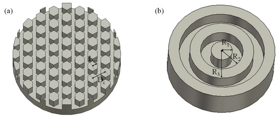
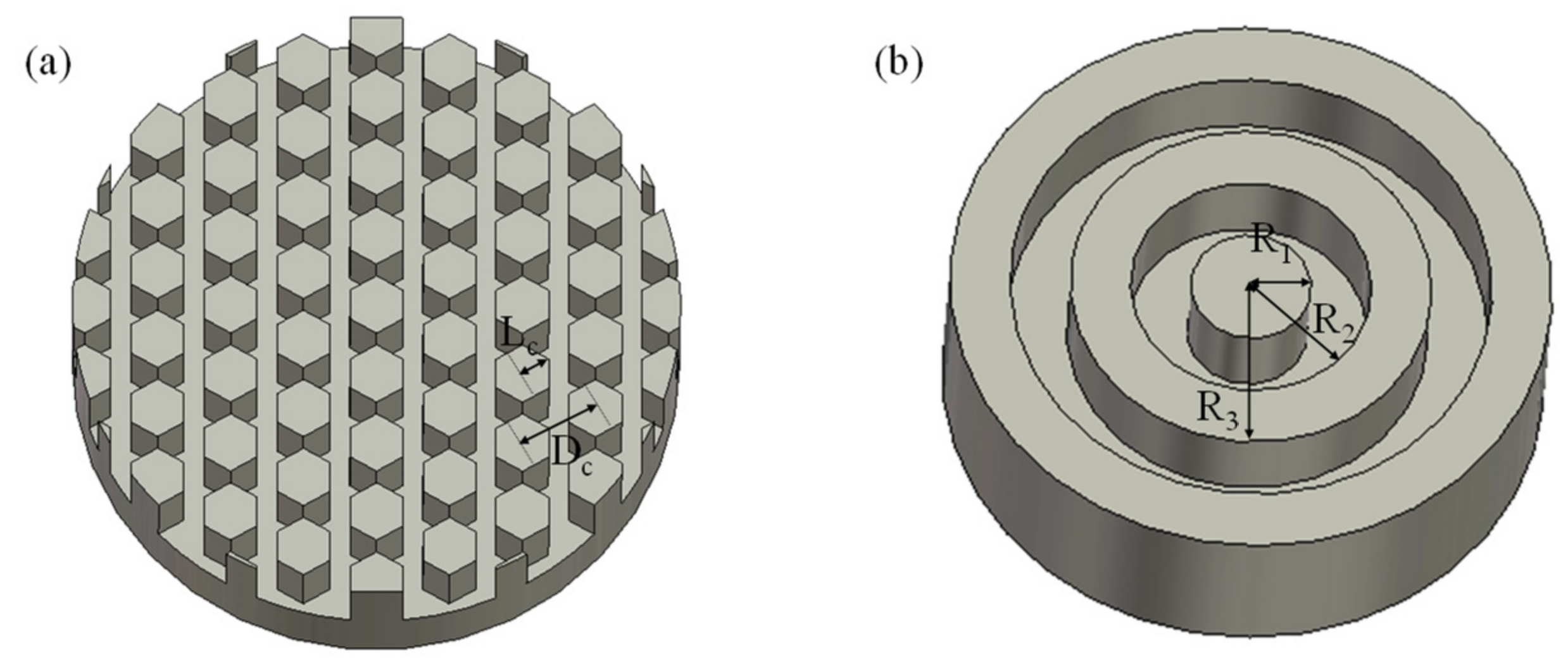
Considering the inherent hard and brittle characteristics of spinel ferrite materials and the structural features verified in previous studies that can effectively trap secondary electrons and restrain their avalanche motion, this paper proposes two innovative periodic physical microstructures for ferrite surface modification. Specifically, two types of periodic raised microstructures, namely hexagonal column arrays and annular protrusion arrays, are designed and fabricated on the surface of spinel ferrites (Figure 1). The customized raised microstructures are intended to adjust the surface morphological characteristics of ferrite materials, build a constrained microenvironment for secondary electron movement, and ultimately suppress the generation and development of multipactor effect. For hexagonal columns, the geometric parameters included side length Lc, center-to-center pitch Dc, and height Hc. For annular structures, the parameters were inner radius R1, outer radius R2, and height Ha.
Figure 1.
Schematic of ferrite surfaces with raised microstructures: (a) hexagonal column array; (b) annular protrusion array.
The hexagonal column array is adopted due to its highest packing density among regular tiling patterns, which maximizes the sidewall area per unit footprint for electron trapping. Its sixfold rotational symmetry ensures isotropic trapping performance regardless of in-plane electron incidence direction, a critical feature for practical microwave devices with multi-directional RF fields. Moreover, the straight-sidewall geometry is compatible with precision mechanical machining of hard and brittle ferrite materials, ensuring good reproducibility and scalability. The annular protrusion array is proposed for offering centrosymmetric geometry and potentially better compatibility with circular device cavities.
2.2. Monte Carlo Simulation of SEY on Structured Surfaces
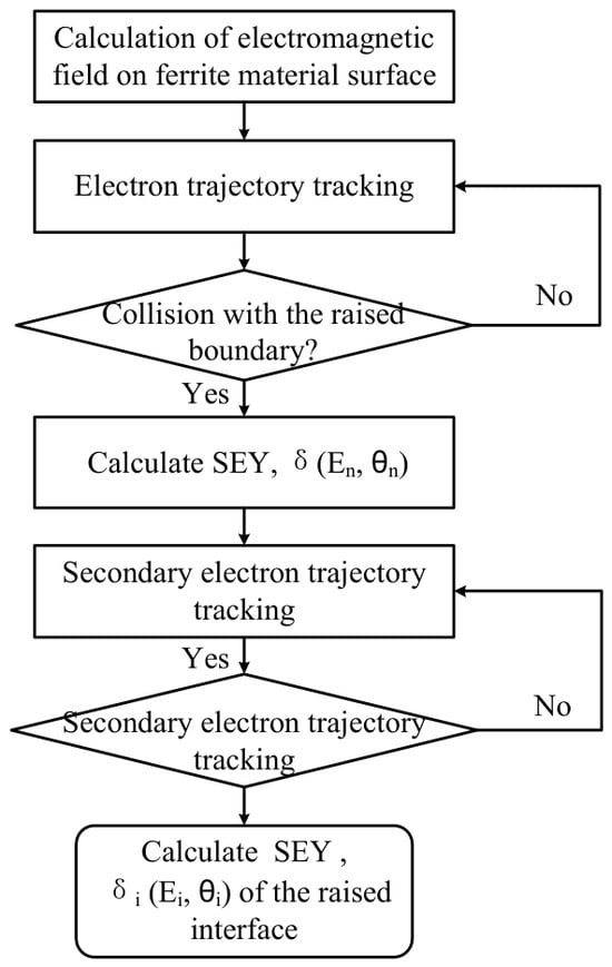
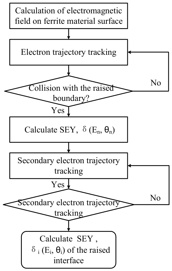
In previous studies, the Monte Carlo method has been widely implemented to simulate and track the dynamic motion trajectories of electrons under electric fields, providing a reliable numerical tool for the quantitative analysis of SEE behavior [4,22]. Building on this foundation, the present work adopts a dedicated Monte Carlo algorithm to accurately calculate the effective SEY of ferrite surfaces with periodic microstructures. The complete workflow of the algorithm, including field calculation, trajectory tracking, and collision modeling, is illustrated in Figure 2.
Figure 2.
Flowchart of the Monte Carlo algorithm for SEY calculation on structured surfaces.
The simulation procedure follows a clear, iterative sequence to model electron behavior:
- (i)
- Electromagnetic Field Calculation: First, the spatial distribution of the RF electromagnetic field on the structured ferrite surface is computed. This field distribution is critical, as it defines the acceleration environment for all charged particles within the simulation domain.
- (ii)
- Primary Electron Trajectory Tracking: The trajectory of each incident primary electron is then tracked in real time, governed by the calculated electromagnetic field.
- (iii)
- Collision Detection and SEE Modeling: As shown in the flowchart, the simulation checks for collisions between the moving electron and the raised microstructures. If a collision occurs, the local SEY is calculated using the probabilistic model for flat ferrite, denoted as δ(En, θn), which is a function of the incident electron energy (En) and angle (θn).
- (iv)
- Secondary Electron Tracking: The generated secondary electrons are then injected into the system, and their trajectories are tracked in the same manner as the primary electrons.
- (v)
- Escape or Absorption Determination: The flowchart explicitly shows that the fate of each secondary electron is determined: it either collides with another surface (leading to further SEE or absorption) or escapes the structured region. If a secondary electron escapes, its contribution to the effective SEY is recorded by calculating δi(Ei, θi) at the raised interface.
When secondary electrons collide with adjacent micro-columns or the bottom substrate surface, two physical outcomes are modeled: the electrons may be directly absorbed by the material, or they may excite further secondary electrons, continuing the avalanche process. In this work, the effective SEY (δeff) is defined as the ratio of the total number of secondary electrons that successfully escape the microstructured ferrite surface to the number of incident primary electrons. This definition acts as a core evaluation index to quantitatively characterize the net SEE suppression performance of the designed surface microstructures.
For a surface with hexagonal columns or annular protrusion arrays, the total SEY per unit area can be approximated as
where A is the area fraction of the gaps between columns, is the SEY of flat ferrite, and δh is the effective SEY of the gap region (which depends on the depth of the gaps).
Equation (1) serves as a simplified area-weighted geometric approximation to reduce computational cost in Monte Carlo simulations for the effective SEY evaluation of structured surfaces. It is not an analytical derivation from first principles, nor does it serve as the primary predictive tool in this work. Rather, it is a heuristic first-order estimate that partitions the total surface into two distinct regions: (i) the top surfaces of the raised microstructures, which are assumed to exhibit the same SEY as a flat ferrite surface (δf), and (ii) the gap (trench) regions between the structures, which are assigned an average effective SEY (δh) that is different from δf due to geometric trapping. The coefficient A denotes the area fraction of the top surfaces relative to the total projected area of the unit cell.
For a surface with hexagonal columns, the simulations considered various Hc, Lc, and Dc values. For a surface with annular protrusion arrays, the simulations considered various R1, R2, and Ha values. The Monte Carlo framework thus provides a particle-level description of the electron dynamics, capturing the detailed geometric effects of the microstructures.
The intrinsic secondary electron yield of smooth spinel ferrite adopted as the collision sub-model within our Monte Carlo framework follows the classical Vaughan empirical SEE model [1],
where denotes the measured maximum secondary electron yield of flat lithium spinel ferrite, is the kinetic energy of incident primary electrons, is the incident angle, corresponds to the primary energy generating peak SEY on smooth ferrite, and is a material-dependent fitting coefficient calibrated against our experimental SEY curves for unstructured ferrite surfaces. This analytical function quantifies the baseline SEE characteristic of flat ferrite and serves as the fundamental local collision yield calculation module throughout all structured-surface Monte Carlo simulations in this paper.
It should be noted that the present Monte Carlo model does not incorporate space charge effects; i.e., the self-consistent electric field arising from trapped charges within the ferrite bulk or on the microstructure surfaces is not computed. This simplification is justified by two considerations. First, the simulation is intended to evaluate the geometric trapping efficiency of the raised microstructures under low-fluence primary electron irradiation, where charging-induced field perturbations are expected to be minimal. Second, the experimental SEY characterization in this work employs pulsed electron beams with low current density and sufficient inter-pulse relaxation intervals, which effectively suppress surface charge accumulation and ensure that the measured SEY approaches the intrinsic material response. This treatment is consistent with previous Monte Carlo studies on SEY from structured surfaces, where space charge effects are often neglected for static yield calculations under well-grounded or charge-neutralized conditions.
2.3. Sample Fabrication
In the study, the spinel ferrite material adopted for all test samples is lithium ferrite (LiFe5O8), the standard spinel ferrite widely deployed in spaceborne microwave-band circulators and isolators. Its key electromagnetic parameters at operating X-band frequency are: relative permittivity εᵣ = 8.9, dielectric loss tanδ = 3.0 × 10⁻⁴, saturation magnetization 4πMs = 0.32 T, and resonance line width ΔH = 150 Oe.
Spinel ferrite disks with a radius of 5 mm were fabricated via precision mechanical processing to realize the designed periodic microstructures on their surfaces. Given the inherent high hardness and brittleness of spinel ferrite materials, which make them highly susceptible to chipping, cracking, and dimensional errors during machining, the fabrication conditions were systematically optimized. Key process parameters, including cutting speed, feed rate, tool geometry, and cooling conditions, were carefully adjusted to minimize surface damage and ensure high geometric accuracy of the microstructures.
A CNC engraving and milling machine is employed to machine ferrite-based hard and brittle materials. The process parameters are as follows: spindle speed of 12,000 rpm, feed rate of 60 to 100 mm/min, and depth of cut of 0.05 to 0.1 mm. Water-soluble cooling liquid is continuously supplied during the whole cutting process to suppress brittle crack propagation of ferrite substrates. After precision machining, the arithmetic average surface roughness Ra measured on the top surfaces of microprotrusions and the bottom surfaces of micro-grooves reaches 0.8 μm. The dimensional tolerance of all geometric features of microstructures (height, side length, radius and array pitch) is strictly controlled within ±0.03 mm.
It should be noted that while the measured surface roughness (Ra = 0.8 μm) is relatively high compared to polished metal surfaces, it remains two orders of magnitude lower than the characteristic dimensions of the raised microstructures (height 1.5 mm, side length 0.5 mm). Therefore, the observed SEY suppression is predominantly governed by the macroscopic geometric trapping effect rather than by sub-micrometer roughness variations. Furthermore, the same machining conditions were applied to all samples, ensuring a consistent baseline surface quality for fair comparison between flat, hexagonal, and annular configurations.
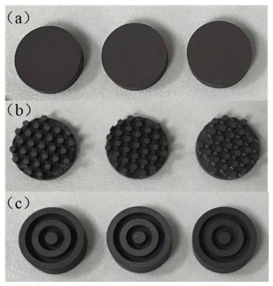
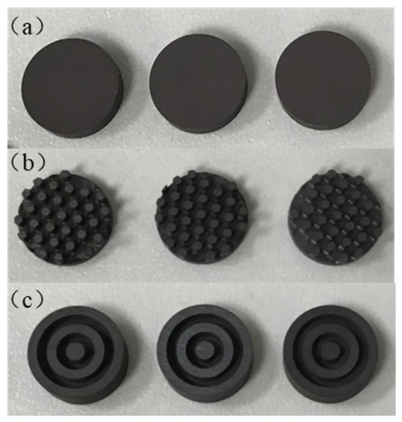
The fabricated hexagonal column array has the following parameters: height Hc = 1.5 mm, side length Lc = 0.5 mm, and center-to-center spacing Dc = 1.67 mm. The annular protrusion arrays have three concentric rings (heights 1.5 mm): inner ring radius 1 mm, middle ring inner/outer radii 2 mm/3 mm, and outer ring inner/outer radii 4 mm/5 mm. Figure 3 shows the fabricated samples: (a) smooth surface (reference), (b) hexagonal column array, and (c) annular protrusion arrays.
Figure 3.
Photographs of spinel ferrite samples: (a) flat surface; (b) with hexagonal column array; (c) with annular protrusion arrays.
2.4. SEY Measurement
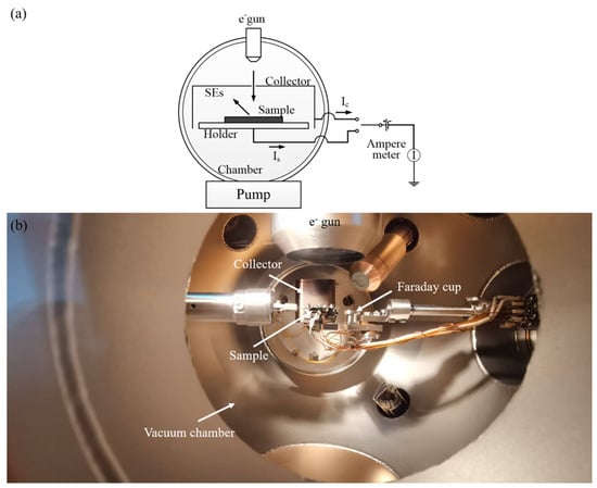
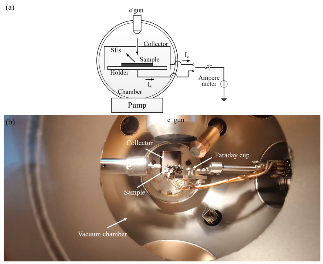
Owing to the inherently low electrical conductivity of ferrite materials, conventional direct-current measurement methods, such as the simple sample current readout technique widely adopted for conductive metal surfaces, are not applicable for accurately determining the SEY. This limitation arises because low-conductivity ferrites cannot efficiently dissipate accumulated surface charges, leading to charging effects that severely distort the measured secondary electron current. To address this challenge, we employed the Faraday cup collector method, which is particularly suited for characterizing the SEY of dielectric and semi-insulating materials. A schematic diagram and picture of the experimental setup are presented in Figure 4 [23]. In this configuration, the primary electron beam is first collected by an isolated Faraday cup to accurately measure the incident current Ii. This measurement is performed with a +500 V bias applied to the cup, ensuring that all incident electrons are captured and any backscattered electrons are suppressed. Subsequently, the ferrite sample is positioned at the measurement station, and the secondary electrons emitted from the sample surface are collected by a separate collector electrode. To ensure efficient collection of all emitted secondary electrons, a positive bias voltage of +20 V is applied to the collector, which attracts low-energy secondary electrons while repelling any stray primary electrons. Simultaneously, a negative bias of −20 V is applied to a surrounding guard ring to confine the collection field and prevent the escape of secondary electrons from the collector cavity, thereby minimizing measurement errors. The collected secondary electron current Is is then measured.
Figure 4.
SEY measurement: (a) schematic of the collector method [23]; (b) picture of the SEY test platform.
The SEY is given by
As shown in Figure 4b, the Faraday cup collector has an inner cylindrical diameter of 8 mm and cavity depth of 12 mm. The vertical distance between the ferrite sample surface and the Faraday cup inlet aperture is fixed at 10 mm for all measurement groups. The vacuum chamber maintains a stable base pressure of 3.2 × 10⁻⁷ Pa during all SEY test cycles to eliminate interference from residual gas ionization collisions.
Lithium ferrites for GHz microwave devices possess ultra-low conductivity, which easily causes surface charge accumulation during electron irradiation and biases SEY data. We adopted 10μs narrow electron pulses separated by a 1 s charge-dissipation gap, and the secondary electron waveforms of five consecutive pulses, which perfectly overlap without signal degradation. Compared with flat square-wave signals from conductive metals and continuously decaying secondary electron signals from poorly optimized dielectrics (due to cumulative trapped charges), the consistent pulse responses in our ferrite tests confirm that the 1 s inter-pulse interval enables full relaxation of surface charges. This pulsed measurement protocol thoroughly mitigates dielectric charging effects and ensures reliable SEY evaluation of ferrites.
3. Results
3.1. Simulation Results for Hexagonal Column Arrays
The SEY simulations are performed on ferrites with different raised microstructures using the Monte Carlo method presented in Section 2.2. In the simulations, the primary electron beam is modeled as a parallel beam with a uniform spatial distribution over the unit cell of the periodic structure. The incident energy is swept from 20 eV to 2000 eV, consistent with the energy range relevant to multipactor in ferrite-loaded microwave devices. For the results presented in the main text, the primary electrons are injected at normal incidence (θn = 0° relative to the surface normal) unless otherwise stated. The angular distribution of the incident beam is assumed to be monodirectional; i.e., all primary electrons share the same incident angle for a given simulation run, which allows systematic investigation of the angular dependence.
The SEE model for the flat ferrite surface follows the standard Vaughan semi-empirical formula. The energy of emitted secondary electrons is sampled from a Maxwellian distribution with a most probable energy of 2 eV, and the emission angle follows a cosine law, as is typical for secondary electrons. For each primary electron, the number of secondary electrons generated is determined by the local SEY, δ(En, θn), where En and θn are the impact energy and angle at the collision point. The trajectory of each secondary electron is then tracked until it either escapes the structured region or is absorbed after multiple collisions.
The key simulation parameters are summarized in Table 2 below for clarity.
Table 2.
Key Monte Carlo simulation parameters.
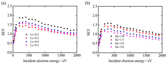
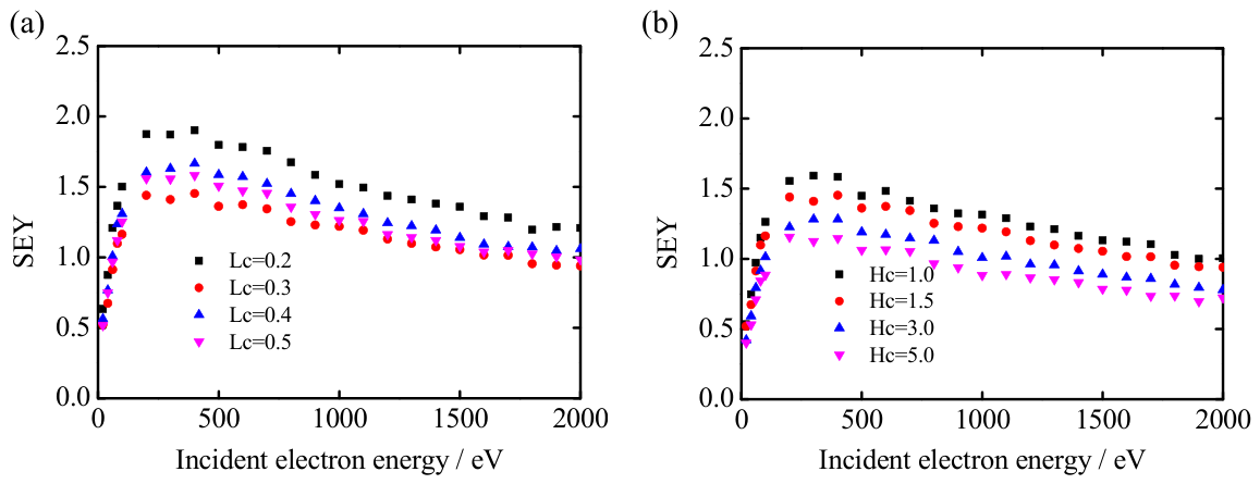
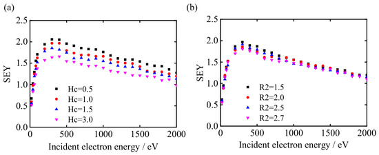
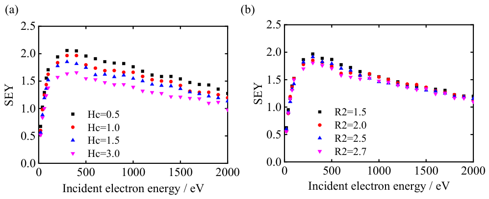
Figure 5 shows simulated SEY curves for hexagonal column arrays with different parameters. For a fixed height Hc and spacing Dc, the effective SEY first decreases and then increases as the side length Lc decreases (Figure 5a). The reduction is attributed to the competition between the increased area of ferrite tops and the reduced gap area where electrons can be trapped. As Lc increases from 0 to 0.3 mm, δeff decreases; beyond 0.3 mm up to 0.5 mm, the trend depends on specific dimensions. Figure 5b shows that for fixed Lc and Dc, δeff decreases monotonically with increasing height Hc. Thus, sufficiently tall columns are required for effective SEY suppression.
Figure 5.
Simulated SEY of hexagonal column arrays: (a) effect of side length Lc (fixed Hc = 1.5, Dc = 1.67); (b) effect of height Hc (fixed Lc = 0.5 mm, Dc = 1.67 mm).
For the hexagonal column arrays with fixed height Hc = 1.5 mm and pitch Dc = 1.67 mm, the maximum SEY (δmax), the first crossover energy (E1) and the average SEY (δave) over the incident energy range of 20 to 2000 eV for each side length Lc are summarized in Table 3 below.
Table 3.
SEY quantitative analyses for hexagonal column arrays.
The data show that δmax decreases from 1.9 at Lc = 0.2 mm to a minimum of 1.45 at Lc = 0.3 mm, then slightly increases to 1.58 at Lc = 0.5 mm. The average SEY follows the same trend, with a minimum of 1.12 at Lc = 0.3 mm. While the differences between Lc = 0.3, 0.4, and 0.5 mm are indeed modest (within approximately 7% in δmax), the optimum at Lc = 0.3 mm is consistently identified by both metrics.
The physical origin of this optimum can be understood through the competition between two opposing geometric effects. When the side length is too small (Lc = 0 to 0.2 mm) and the center-to-center pitch is a certain dimension, the flat surfaces of the columns constitute a large fraction of the total surface area relative to the gaps. Since the flat top surfaces retain the intrinsically high SEY of the ferrite material (δmax = 2.4), electrons impacting these regions are emitted with high probability, thereby diminishing the overall suppression efficiency. Conversely, when the side length becomes too large (Lc = 0.4 to 0.5 mm), the inter-column gaps narrow considerably. This restricts the space available for secondary electrons to undergo multiple scattering events with the sidewalls, reducing the trapping probability and allowing a greater proportion of electrons to escape. The optimum at Lc = 0.3 mm represents a balance where the gap width is sufficiently wide to enable effective multiple reflections and absorption, while the top surface area remains small enough to limit direct high-yield emissions. This interpretation is consistent with the general understanding that the electron trapping efficiency of a microcavity structure is governed by the aspect ratio and the fractional area of the emitting surfaces.
Nevertheless, in practical device applications, the selection of the hexagonal column parameters should be balanced against the electrical performance requirements of the specific component, including considerations such as insertion loss, impedance matching, and field uniformity. The final design thus represents a compromise between SEY suppression efficiency and overall device functionality.
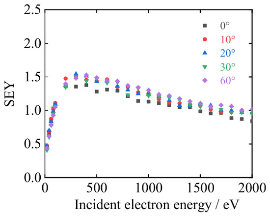
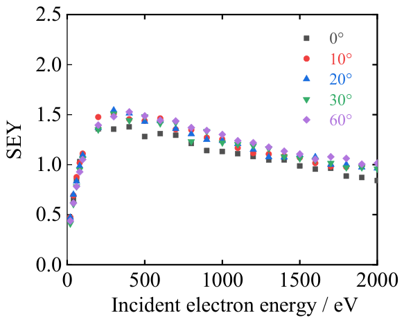
The simulations have been extended to evaluate the effective SEY of the hexagonal column array (Hc = 1.5 mm, Lc = 0.4 mm, Dc = 1.2 mm) for primary electrons incident at angles θ = 0°, 10°, 20°, 30°, and 60° relative to the surface normal. The results are presented in Figure 6.
Figure 6.
Simulated effective SEY of the hexagonal column array as a function of primary electron incidence angle.
For the flat ferrite surface, the SEY increases monotonically with incidence angle, which is consistent with the well-known angular dependence of SEE: as θ increases, the path length of primary electrons near the surface becomes longer, leading to more electron–hole pair generation and thus higher SEY. For the structured surface, the effective SEY also increases with θ, but the increase is significantly suppressed for angles up to about 60°. In practical microwave devices, the electron impact angle distribution often peaks around 30° to 60°, so the approach remains highly relevant.
3.2. Simulation Results for Annular Protrusion Arrays
For annular protrusion arrays (Figure 7a), increasing the ring height reduces δeff. When the cross-sectional shape of the rings is varied (e.g., reducing the inner radius), the effective SEY changes according to the gap area and the SEY of the gap region (Figure 7b). In all cases, deeper gaps lead to lower δeff.
Figure 7.
Simulated SEY of annular protrusion arrays: (a) effect of ring height; (b) effect of ring cross-section geometry.
3.3. Experimental Validation of SEYs
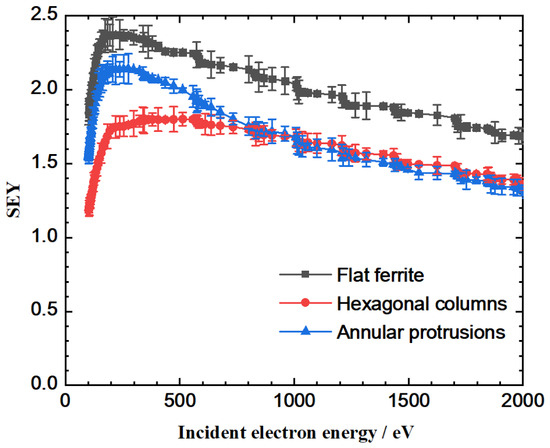
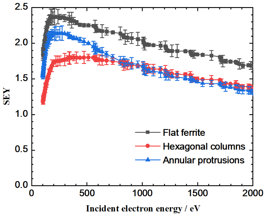
The prepared ferrite samples shown in Figure 3 were characterized using the setup illustrated in Figure 4, and the corresponding SEY test results were obtained as shown in Figure 8. Although the use of microsecond-scale short pulses in SEY measurements effectively mitigates surface charge accumulation, residual errors persist due to transient surface modifications induced by the incident current pulse. These include dynamic changes in the electron emission barrier caused by concomitant charge buildup and gas desorption, as well as trajectory perturbations of low-energy emitted electrons, all of which modulate the apparent SEY. Furthermore, the surface condition may not be fully restored between successive pulses, compromising measurement repeatability. Additional contributions from system response hysteresis and parasitic noise in the microsecond-scale pulsed current further degrade signal stability. Consequently, each test cycle is effectively non-identical, introducing systematic uncertainties that cannot be adequately quantified by simple averaging.
Figure 8.
Measured SEY curves for flat, hexagonal-structured, and annular-structured ferrite samples.
As a baseline reference, the flat, unstructured ferrite surface exhibits a maximum SEY of 2.4, which is consistent with the typical high-SEY characteristics of spinel ferrites. For the sample with hexagonal column arrays (column height: 1.5 mm, side length: 0.5 mm, center-to-center spacing: 1.67 mm), the maximum SEY drops significantly to 1.7, representing a reduction of approximately 29% compared to the flat counterpart. In contrast, the annular protrusion arrays yield a moderate improvement, with the maximum SEY decreasing to 2.1, corresponding to a 12.5% reduction. The experimental results clearly confirm that the proposed raised microstructures can effectively regulate and suppress the SEY of ferrite surfaces by trapping secondary electrons and altering their emission trajectories. However, the achievable suppression performance is constrained by the inherent high hardness and brittleness of ferrite materials, which limit the minimum feature size and aspect ratio that can be reliably fabricated, thus imposing an upper bound on the effectiveness of this purely geometric mitigation strategy.
3.4. Device-Level Validation
To strengthen the validation pathway, we have initiated the design of X-band high-power wideband Y-junction ferrite circulators as a platform for device-level characterization. X-band (8 to 12 GHz) was selected for the following reasons: (i) it is a standard frequency band for high-power spaceborne radar and communication systems, where multipactor suppression is critically needed; (ii) ferrite circulators in this band have been extensively characterized in the literature, providing a reliable benchmark for comparison; and (iii) the wavelength at X-band (approximately 25–37 mm) remains significantly larger than our microstructure feature sizes, making it a suitable testbed for evaluating potential RF perturbations.
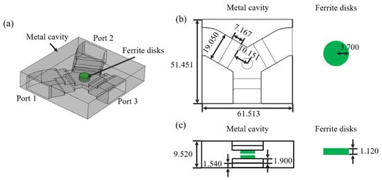
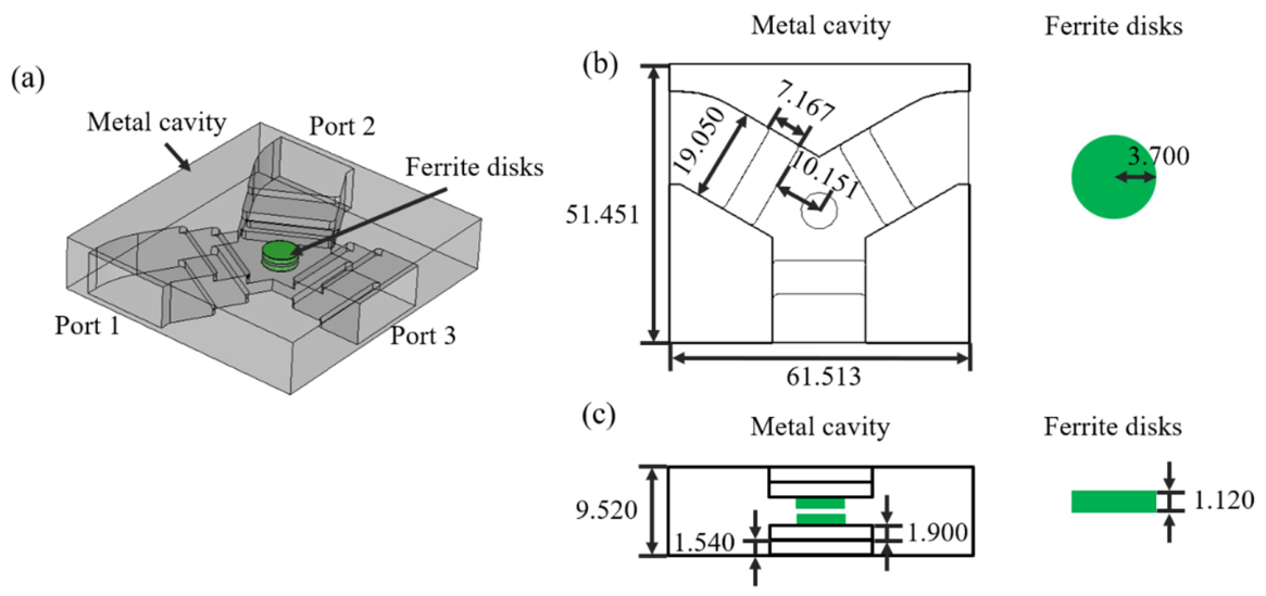
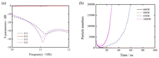
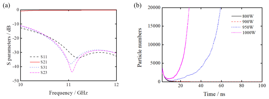
Based on the promising results obtained for the hexagonal column arrays, an X-band high-power wideband Y-junction ferrite circulator has been designed to serve as a platform for device-level validation. The circulator is designed using a Y-junction configuration with a spinel ferrite disk at the junction, following established design principles for X-band operation. As shown in Figure 9, the initial electromagnetic design and optimization are performed using a 3D full-wave electromagnetic simulator. Simulation results for the S parameters and multipactor threshold are given in Figure 10.
Figure 9.
The designed X-band ferrite circulator, (a) 3D model, (b) dimensions in the top view (unit: mm), (c) dimensions in the side view (unit: mm).
Figure 10.
Simulation results for the X-band circulator with flat ferrite disks, (a) S parameters, (b) particle number evolutions using the EM-PIC method.
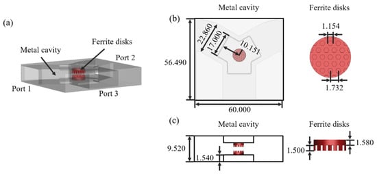
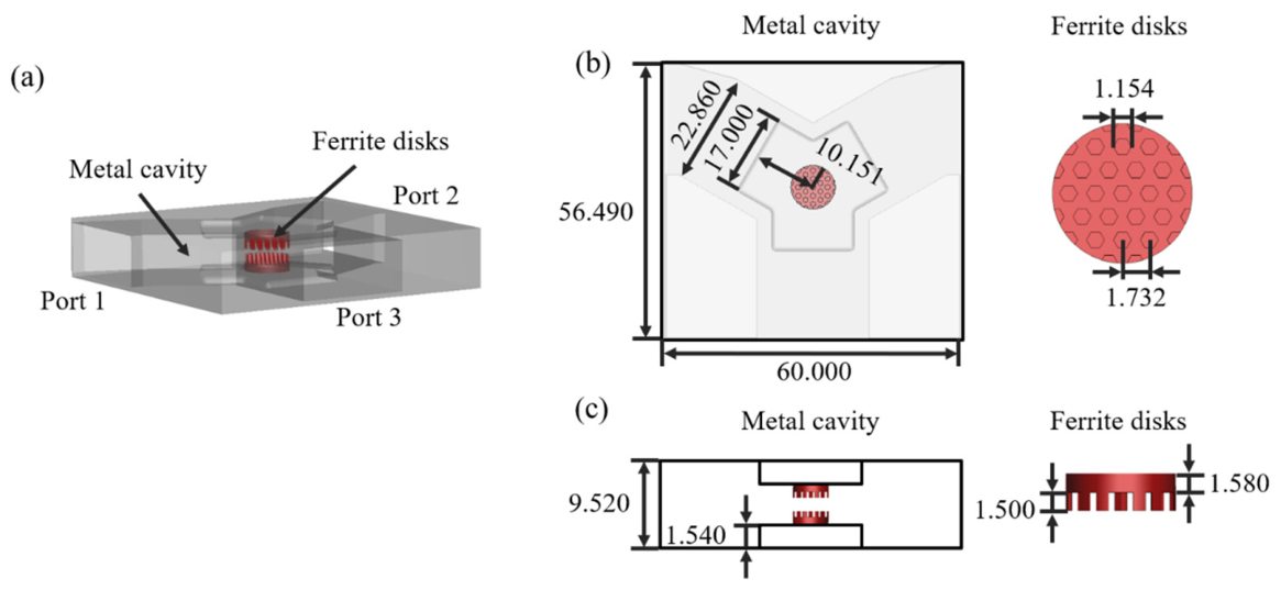
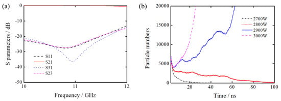
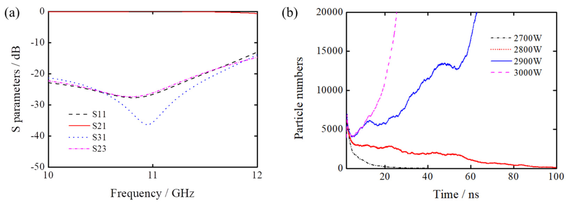
For the anti-multipactor design, the hexagonal column microstructure has been implemented on the ferrite substrates, which is the region where multipactor discharge is most likely to be initiated due to the high RF field concentration, as shown in Figure 11. Specifically, guided by the simulation and experimental results that determined the optimal geometric parameters, a hexagonal-structured ferrite with a column height of 1.500 mm, side length of 0.577 mm, and pitch of 1.732 mm was adopted for circulator design. This configuration simultaneously achieves prominent SEY suppression and favorable electrical performance of the circulator. Simulation results for the S parameters and multipactor threshold are given in Figure 12.
Figure 11.
The designed X-band ferrite circulator with hexagonal raised microstructures on ferrite disks, (a) 3D model, (b) dimensions in the top view (unit: mm), (c) dimensions in the side view (unit: mm).
Figure 12.
Simulation results for the X-band circulator with hexagonal raised microstructures on ferrite disks, (a) S parameters, (b) particle number evolutions using the EM-PIC method.
To quantitatively assess the improvement in multipactor performance, we employed a rigorous EM-PIC tracking simulation on the circulators. Effects of the periodic raised microstructures have been validated through EM-PIC simulations, which predict electron multiplication within the circulator under high-power RF excitation.
The simulated S parameters and multipactor thresholds are summarized in Table 4 below.
Table 4.
The simulated S parameters and multipactor thresholds.
It should also be emphasized that these EM-PIC results are still preliminary and serve as a first-order device-scale validation of the multipactor suppression capability. Physical prototype fabrication and high-power vacuum multipactor tests are planned in our future work to provide full experimental device validation.
4. Discussion
Combined simulation and experimental results confirm that the periodic raised microstructures fabricated on spinel ferrite surfaces effectively suppress secondary electron emission and significantly reduce the effective secondary electron yield (SEY), even at oblique incidence, where the secondary electron emission is also well suppressed. The dominant physical mechanism is attributed to the geometric electron trapping effect induced by the patterned surface morphology. Secondary electrons generated inside the gaps of periodic protrusive structures experience repeated collision and reflection with the sidewalls and bottom substrate, which greatly increases the probability of material absorption. Consequently, most secondary electrons are consumed during multiple scattering processes rather than escaping from the surface to form continuous electron avalanches. Further analysis reveals that the SEY suppression performance is positively correlated with the structural aspect ratio (height-to-width ratio). Microstructures with higher aspect ratios form deeper and narrower confined gaps, which provide more sufficient collision paths and absorption opportunities for secondary electrons, thereby achieving better suppression effects. This variation law is highly consistent with Monte Carlo simulation results, where the effective SEY continuously decreases as the structural height Hc increases (Figure 5b). Notably, hexagonal column arrays exhibit an optimal side length range for SEY suppression. Excessively large column sizes reduce the gap spacing and effective trapping area, while undersized columns enlarge the proportion of flat top surfaces with high SEY characteristics. Both extreme structural conditions weaken the overall electron trapping capacity, resulting in degraded secondary electron suppression performance.
The superior SEY suppression of hexagonal columns over annular structures can be attributed to their higher sidewall density and more effective confinement of secondary electrons within the gaps. For the same occupied footprint, hexagonal arrays provide a larger total trapping area and deeper potential wells for multiple scattering, leading to enhanced absorption of secondary electrons. This geometric advantage, combined with fabrication practicality and isotropic performance, makes the hexagonal pattern a well-balanced choice for ferrite surface engineering. Future optimization may explore other high-symmetry lattices, such as honeycomb or kagome, to further improve suppression efficiency.
Compared with previously reported ferrite surface modification strategies, the proposed direct microstructure machining method possesses prominent advantages in interfacial adhesion and mechanical stability. Coating-based modification techniques are prone to interfacial peeling, layer shedding and structural failure under harsh aerospace operating conditions, including high-intensity mechanical vibration and alternating thermal cycling. In contrast, the integrally machined raised microstructures are inherently consistent with the ferrite substrate, eliminating the risk of coating delamination and ensuring long-term structural reliability for spaceborne microwave devices. In addition, this pure geometric modification strategy does not introduce any foreign auxiliary materials, which completely avoids the outgassing contamination, material aging and dielectric performance degradation caused by additive materials under high-power vacuum operating environments. In this work, the maximum SEY of the structured ferrite surface is successfully reduced from 2.4 to 1.7, which represents a significant performance improvement. It is widely acknowledged that an SEY value below 1.5 is the critical threshold for stable anti-multipactor operation of vacuum microwave devices. Therefore, further optimization of structural parameters, including appropriately increasing the microstructure height beyond 1.5 mm and reducing the gap width to enhance electron confinement, is expected to further lower the effective SEY. Such performance upgrades can be realized with the continuous improvement of precision microfabrication technologies for hard and brittle ferrite materials, such as laser micromachining and ultra-precision micro-milling.
Under the same structural height condition, the annular protrusion array achieves a relatively limited SEY suppression effect, with the maximum SEY only decreasing to 2.1. The performance discrepancy between the two microstructures stems from their inherent geometric differences. With the same overall occupied area on the ferrite surface, the annular protrusion structure provides fewer vertical sidewalls and a smaller effective electron trapping area than hexagonal column arrays. The open annular gap structure cannot effectively constrain and trap secondary electrons, resulting in a higher proportion of escaping electrons and weaker SEY suppression capability. Nevertheless, annular protrusion arrays exhibit unique application potential in practical engineering. Benefiting from their centrosymmetric geometric characteristics, they enable isotropic electron trapping in all in-plane directions and show better structural compatibility with circular and coaxial microwave device cavities. Accordingly, hybrid composite microstructures and multi-parameter optimized annular structural designs will be explored in future research to balance isotropic performance and secondary electron suppression efficiency.
Simulation results of device-level validation show that the hexagonal raised microstructures increase the device multipactor power threshold from 900 W to 2800 W while the insertion loss is maintained at ≤0.5 dB. It is important to note, however, that the observed difference in multipactor threshold between the two circulator configurations is not attributable solely to the surface microstructures; the device geometry itself also contributes to the modification of the internal RF field distribution, which in turn affects electron trajectories and impact energies. Therefore, the threshold enhancement should be interpreted as a combined effect of the reduced SEY due to the microstructures and the altered electromagnetic field environment resulting from the structural modification of the ferrite disks. Such a device-level adjustment is unavoidable, because the overall circulator must be re-optimized to maintain good electrical performance when the ferrite surface is modified. Nevertheless, this does not diminish the conclusion that the surface microstructures themselves are responsible for a substantial improvement in the multipactor threshold.
5. Conclusions
This work proposes a geometric surface structuring strategy to precisely regulate the SEY of spinel ferrite materials, targeting the suppression of detrimental multipactor discharge in high-power vacuum microwave devices. Given the inherently high SEY of ferrite dielectrics, which severely restricts the multipactor threshold and long-term operational reliability of spaceborne nonreciprocal microwave components, surface microstructural modification is adopted to physically constrain secondary electron motion and inhibit electron avalanche multiplication. To quantitatively evaluate the SEY suppression performance of patterned ferrite surfaces, a dedicated Monte Carlo numerical simulation framework is established to compute the effective SEY of ferrite substrates integrated with hexagonal column arrays and annular protrusion arrays. Based on the constructed simulation model, the intrinsic influence laws of key structural parameters, including structural height, spacing, and feature size, on secondary electron emission characteristics are systematically analyzed, providing theoretical guidance for the structural design of anti-multipactor microstructures. For experimental verification, periodic hexagonal column arrays (height: 1.5 mm, side length: 0.5 mm, spacing: 1.67 mm) and annular protrusion arrays are fabricated on spinel ferrite samples via precision mechanical machining, which adapts to the hard and brittle properties of ferrite materials and ensures high structural consistency. The measured SEY experimental results demonstrate that the optimized hexagonal column microstructure achieves excellent suppression performance, reducing the maximum SEY of flat ferrite from 2.4 to 1.7 with a suppression ratio of approximately 30%. In comparison, the annular protrusion structure also delivers a valid mitigation effect, lowering the maximum SEY to 2.1. Different from conventional coating modification methods that suffer from poor adhesion, outgassing risk and thermal fatigue failure, the proposed all-mechanical surface structuring approach is coating-free and features superior mechanical robustness and environmental adaptability. It effectively avoids foreign material contamination and performance degradation under high-power vacuum and aerospace vibration conditions. This study provides a feasible and reliable technical route for SEY regulation and multipactor suppression of ferrite materials, exhibiting great application potential for improving the high-power bearing capacity and operational stability of spaceborne ferrite circulators, isolators, and other high-power vacuum microwave components.
Author Contributions
Conceptualization, Y.N. and Y.L.; methodology, Y.N., Y.L. and G.F.; software, Y.L. and G.F.; validation, Y.N. and Q.Y.; formal analysis, Y.N.; investigation, Y.N., Y.L., G.F. and Q.Y.; resources, Y.L.; data curation, Y.L.; writing—original draft preparation, Y.N., Y.L. and G.F.; writing—review and editing, Y.L. and G.F.; visualization, Y.L.; supervision, Y.L.; project administration, Y.L.; funding acquisition, Y.L. All authors have read and agreed to the published version of the manuscript.
Funding
This research was funded by the National Key R&D Program (Grant No. 2023YFF0722101), the National Natural Science Foundation of China (Grant Nos. 12175176), and the Youth Top Talent Project of Shaanxi Province Special Support Plan.
Institutional Review Board Statement
Not applicable (this study did not involve humans or animals).
Informed Consent Statement
Not applicable.
Data Availability Statement
The raw data supporting the conclusions of this article will be made available by the authors on request.
Conflicts of Interest
Author Qian Yuan was employed by the company Beijing Aerospace Micro-Electronics Technology co., Ltd. The remaining authors declare that the research was conducted in the absence of any commercial or financial relationships that could be construed as a potential conflict of interest.
References
- Vaughan, J.R.M. Multipactor. IEEE Trans. Electron Devices 1988, 35, 1172–1180. [Google Scholar] [CrossRef] [Scilit]
- Garcia-Patron, M.; Montero, I.; Ruiz-Cruz, J.A. Advanced multipactor testing with enhanced power efficiency for space applications. IEEE Trans. Instrum. Meas. 2025, 74, 8000815. [Google Scholar] [CrossRef] [Scilit]
- Guillén, C.A.; Jódar, M.R.; Marín, R.C.; Morro, J.V.; Soto, P.; Monerris, S.; Ossorio, J.; Mata, R.; Smacchia, D.; Boria, V.E. A Fast and Accurate Coarse Method for Multipactor Threshold Prediction of RF Filters Under Modulated Signal Excitation. IEEE Trans. Electron Devices 2025, 72, 3177–3184. [Google Scholar] [CrossRef] [Scilit]
- Feng, G.; Liu, L.; Cui, W.; Wang, R.; Hu, T. Transient Characteristics of Charging Effects due to E-Beam Irradiation: A Method of SEY-Based Charging Balance Mode. IEEE Trans. Plasma Sci. 2019, 47, 3783–3789. [Google Scholar] [CrossRef] [Scilit]
- Cao, K.H.; Song, B.P.; You, Y.N.; Li, H.P.; An, W.T.; Liu, Y.T.; Zhang, G.J. Research on the double-sided surface flashover characteristics of the irregular ceramic insulator in high-power electron guns. J. Appl. Phys. 2025, 138, 213302. [Google Scholar] [CrossRef] [Scilit]
- Zhang, G.J.; Sun, G.Y.; Song, B.P.; Neuber, A.; Yamano, Y. Global model for flashover phenomena in vacuum: A comprehensive perspective. J. Appl. Phys. 2025, 137, 103301. [Google Scholar] [CrossRef] [Scilit]
- Mao, Z.S.; Li, Y.; Cai, Y.H.; He, Y.N.; Yu, M. Experimental investigation of material and geometry effects on microwave breakdown of evanescent-mode cavity resonators. IEEE Trans. Microw. Theory Tech. 2021, 69, 4001–4009. [Google Scholar] [CrossRef] [Scilit]
- An, W.T.; Song, B.P.; Zou, F.Z.; Sun, G.Y.; Liu, Y.T.; Li, H.P.; Deng, J.Q.; Qin, X.G.; Zhang, G.J. Charge dynamics in spacecraft polymers: Trap-modulated mechanisms from bulk accumulation to surface secondary electron emission. AIP Adv. 2025, 15, 115114. [Google Scholar] [CrossRef] [Scilit]
- Spencer, H.; Wright, D.; Gregory, A.; Mankowski, J.; Stephens, J.; Dickens, J.; Neuber, A. Evaluation of methods to counteract multipactor phenomena in X-band waveguides. Phys. Plasmas 2024, 31, 033101. [Google Scholar] [CrossRef] [Scilit]
- Vague, J.; Melgarejo, J.C.; Boria, V.E.; Guglielmi, M.; Moreno, R.; Reglero, M.; Mata, R.; Montero, I.; González-Iglesias, D.; Gimeno, B.; et al. Experimental Validation of Multipactor Effect for Ferrite Materials Used in L- and S-Band Nonreciprocal Microwave Components. IEEE Trans. Microw. Theory Tech. 2019, 67, 2151–2161. [Google Scholar] [CrossRef]
- Ren, H.; Xie, Y. Simulations of the Multipactor Effect in Ferrite Circulator Junction With Wedge-Shaped Cross Section Geometry. IEEE Trans. Electron Devices 2020, 67, 5144–5150. [Google Scholar] [CrossRef] [Scilit]
- Jiang, L.; Yang, F.; Cui, Z.; Yang, J. Ridged structure of coaxial cavity for raising the multipactor threshold of microwave switch. IEEE Access 2024, 12, 105761–105765. [Google Scholar] [CrossRef] [Scilit]
- Iqbal, A.; Wen, D.Q.; Verboncoeur, J.; Zhang, P. Recent advances in multipactor physics and mitigation. High Volt. 2023, 8, 1063–1082. [Google Scholar] [CrossRef] [Scilit]
- Wright, D.; Shaw, Z.C.; Mankowski, J.J.; Dickens, J.C.; Stephens, J.; Neuber, A.A. Multipactor suppression via asymmetric grooves in S-band waveguide. Phys. Plasmas 2022, 29, 063101. [Google Scholar] [CrossRef] [Scilit]
- Hseuh, H.; Blaskiewicz, M.; He, P.; Lee, Y.; Pai, C.; Raparia, D.; Todd, R.; Wang, L.; Wei, J.; Weiss, D.; et al. Physical and electromagnetic properties of customized coatings for SNS injection ceramic chambers and extraction ferrite kickers. In Proceedings of the 2005 Particle Accelerator Conference, Knoxville, TN, USA, 16–20 May 2005; pp. 1234–1237. [Google Scholar]
- Yamamoto, K.; Kamiya, J.; Ogiwara, N.; Kinsho, M.; Hayashi, N.; Saeki, R.; Satou, K.; Toyama, T. Estimation of secondary electron effect in the J-PARC rapid cycling synchrotron after first study. Appl. Surf. Sci. 2009, 256, 958–961. [Google Scholar] [CrossRef] [Scilit]
- Lorenz, P.; Himmerlich, M.; Ehrhardt, M.; Bauer, J.; Lotnyk, A.; Bez, E.; Kersten, H.; Zimmer, K. Reactive laser ablation of copper in hydrocarbon atmosphere: Synthesis of nanocomposite surface layers for secondary electron yield reduction. Appl. Surf. Sci. 2026, 732, 166487. [Google Scholar] [CrossRef] [Scilit]
- Uren, R.; Din, A.; Wackerow, S.; Himmerlich, M.; Abdolvand, A. A universal process for reducing secondary electron yield. In Proceedings of the 17th International Conference on Laser Ablation (COLA), Hersonissos, Greece, 29 September–4 October 2024. [Google Scholar]
- Uren, R.; Hoffman, M.; Din, A.; Wackerow, S.; Neupert, H.; Pfeiffer, S.; Moros, A.; Barnes, M.; Favia, G.; Himmerlich, M.; et al. Ferrites with a minimized secondary electron yield. Adv. Sci. 2025, 12, 2410083. [Google Scholar] [CrossRef] [Scilit] [PubMed]
- Li, Y.; Wang, D.; Yu, M.; He, Y.N.; Cui, W.Z. Experimental Verification of Multipactor Discharge Dynamics Between Ferrite Dielectric and Metal. IEEE Trans. Electron Devices 2018, 65, 4592–4598. [Google Scholar] [CrossRef] [Scilit]
- Ye, M.; He, Y.N.; Wang, R.; Hu, T.C.; Zhang, N.; Yang, J.; Cui, W.Z.; Zhang, Z.B. Secondary electron emission suppression by surface micro-structures. Acta Phys. Sin. 2014, 63, 147901. [Google Scholar] [CrossRef] [Scilit]
- Sun, G.Y.; Lian, R.H.; Zhang, S.; Yang, X.; Abbas, M.F.; Wang, C.; Guo, B.H.; Song, B.P.; Zhang, G.J. An alternative simulation approach for surface flashover in a vacuum using a 1D2V continuum and kinetic model. J. Phys. D. Appl. Phys. 2023, 56, 365205. [Google Scholar] [CrossRef] [Scilit]
- Li, Y.; Feng, G.; Li, B.; Zhang, L.; Wang, Y.; Li, X. Enhanced investigation on the low-pressure RF discharge of high-power microstrip circuits under different process conditions. Phys. Plasmas 2026, 33, 033903. [Google Scholar] [CrossRef] [Scilit]

Disclaimer/Publisher’s Note: The statements, opinions and data contained in all publications are solely those of the individual author(s) and contributor(s) and not of MDPI and/or the editor(s). MDPI and/or the editor(s) disclaim responsibility for any injury to people or property resulting from any ideas, methods, instructions or products referred to in the content. |
© 2026 by the authors. Licensee MDPI, Basel, Switzerland. This article is an open access article distributed under the terms and conditions of the Creative Commons Attribution (CC BY) license.