1. Introduction
As Micro-light-emitting diode (MicroLED) technology moves toward ultra-high-definition displays and augmented reality/virtual reality (AR/VR) applications, the industry is shifting from traditional gold-based metallization to Copper (Cu) interconnects [
1]. Cu offers significant advantages in electrical conductivity and low specific contact resistance, which are critical for mitigating current crowding effects and ensuring uniform carrier injection in pixels scaled below 50 μm [
2,
3]. However, the integration of Cu into Gallium Nitride (GaN) structures introduces a significant reliability bottleneck. Unlike stable refractory metals, Cu is a fast diffuser in semiconductors, and its high mobility at elevated temperatures poses a threat to the long-term optoelectronic stability of the III-nitride lattice [
4].
The physical nature of Cu in GaN is characterized by its ability to exist as both an interstitial donor (Cu
i) and a substitutional acceptor (Cu
Ga) [
5]. Because heteroepitaxial GaN on Silicon typically contains a high density of threading dislocations (TDs) (10
9–10
10 cm
−2), these defects act as “fast-track” diffusion paths, allowing Cu ions to bypass bulk lattice resistance [
6,
7]. Once Cu atoms migrate into the active region, they create vacancy like defects that act as Shockley Read Hall non radiative recombination centers [
8,
9], thereby dissipating energy as heat and reducing the internal quantum efficiency [
10]. Furthermore, the high perimeter-to-area ratio of MicroLEDs leads to a significant exposure of sidewall defects, which can act as preferential pathways for Cu diffusion.
Studies have shown that Cu encroachment results in increased reverse leakage currents and threshold voltage shifts [
11], eventually leading to pixel crosstalk or complete device failure. Despite these risks, comprehensive research linking Cu diffusion kinetics to specific failure modes remains limited. This study aims to fill that gap by analyzing the diffusion profiles of Cu in GaN-based devices and evaluating the efficacy of Ni, Ti, and Pt barriers for future high-reliability display applications.
The migration of Cu in GaN is governed by the kick-out mechanism, where interstitial Cu atoms displace Ga atoms from their lattice sites. During thermal annealing, Cu out-diffusion induces the formation of Ga vacancies and their clustering [
9]. In the GaN wurtzite structure, Cu is expected to occupy primarily interstitial lattice positions, with first-principles calculations suggesting that substitutional incorporation at Ga sites (Cu
Ga) is energetically more favorable than interstitial sites (Cu
i) [
12]. As the thermal budget increases, mobile Cu atoms may displace host Ga atoms to occupy substitutional acceptor sites (Cu
Ga), a process that is likely mediated by the concentration of native Ga vacancies (V
Ga) and the Fermi level of the material. This incorporation is predicted to introduce deep-level traps that can effectively pin carriers and act as non-radiative recombination centers, though the exact energy levels require further experimental validation.
The kinetics of Cu diffusion are dramatically accelerated by the high density of structural defects inherent in GaN-on-Si epitaxial layers. Threading dislocations, which typically range from 10
8 to 10
10 cm
−2 in heteroepitaxial GaN [
13], serve as “short-circuit” or pipe diffusion paths. The localized strain fields and reduced atomic packing density at dislocation cores significantly lower the activation energy for atomic hopping compared to bulk lattice diffusion. According to first-principles calculations, the diffusivity of point defects can be modified by up to 50% in the vicinity of threading dislocations [
14]. Theoretical studies also indicate that point defects, including Ga vacancies and oxygen-related complexes, can be trapped in the stress field of extended defects, potentially creating a pathway for Cu to bypass the p-GaN layer and penetrate the multiple quantum well region under sufficient thermal stress.
Furthermore, the diffusion process in active MicroLEDs can be influenced by the synergy of thermal gradients and electric field-induced drift. It has been observed that field-induced migration of shallow donors occurs in GaN p-i-n junctions under applied electric fields [
15], suggesting that a similar mechanism could drive the drift of positively charged Cu interstitials in the high internal fields (>10
5 V/cm) characteristic of p-n junctions. This field-enhanced migration is further exacerbated by self-heating effects; localized hot spots near the micro-junctions raise the diffusion coefficient exponentially according to the Arrhenius relationship. The resulting accumulation of Cu atoms may lead to the formation of Cu-vacancy complexes and metallic precipitates, which serve as localized shunt paths and non-radiative recombination centers that degrade the device’s internal quantum efficiency, though direct experimental evidence for these specific degradation products in MicroLEDs remains limited.
2. Materials and Methods
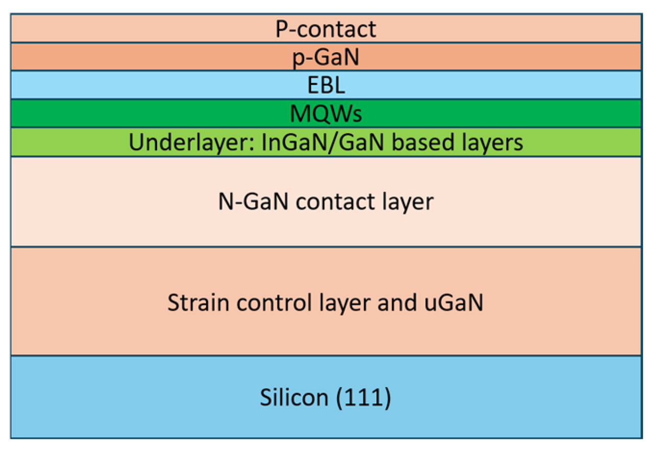
The green GaN-on-Silicon epitaxial wafers used in this study were supplied by Suzhou Hanhua Semiconductor Co., Ltd., Suzhou, China, and grown by metal–organic chemical vapor deposition (MOCVD) on 200 mm (111)-oriented Si substrates. As illustrated in
Figure 1, the epilayer stack consists from bottom to top of an AlN/AlGaN strain control buffer layer to mitigate the mismatch in lattice constant and thermal expansion coefficient between GaN and Si; a high-quality unintentionally doped GaN (u-GaN) layer; a Si-doped n-GaN contact layer (~1 μm thick); an InGaN/GaN-based strain-releasing underlayer; an InGaN/GaN multiple quantum well (MQW) active region with a peak emission wavelength of approximately 520 nm; and finally a Mg-doped p-GaN hole injection layer. An indium tin oxide (ITO) transparent conductive layer was deposited on top of the p-GaN to facilitate current spreading.
A dual-lithography strategy was employed: positive photoresist defined the mesa areas, followed by ICP etching (Cl2/BCl3) to expose the n-GaN. A negative photoresist process was then used to obtain a conical mesa sidewall geometry via lift-off, with a mesa radius of 175 μm. Notably, because this study is dedicated to evaluating Cu diffusion barrier performance, the mesa size (350 μm diameter) lies well outside the MicroLED regime (<100 μm), thereby minimizing sidewall effects and enabling a clear assessment of Cu migration in GaN.
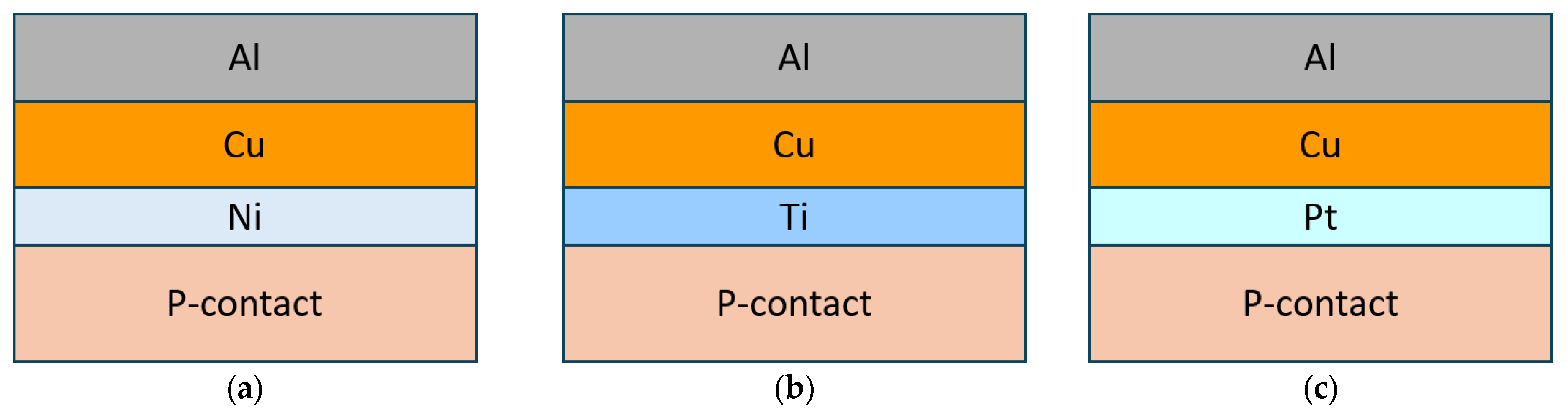
Three metallization schemes were deposited by electron beam evaporation: Ni/Cu/Al, Ti/Cu/Al, and Pt/Cu/Al, as schematically depicted in
Figure 2a–c, respectively. The thicknesses were fixed at 10 nm for the barrier/adhesion layer (Ni, Ti, or Pt), 400 nm for the Cu layer, and 400 nm for the Al capping layer.
Samples were subjected to four thermal conditions: as-deposited (unannealed), and isothermal annealing at 100 °C, 200 °C, and 300 °C for 2 h in an N2 ambient. This simulates back-end-of-line (BEOL) thermal budgets and device self-heating.
Electrical integrity was quantified through Current-Voltage (I-V) measurements. Optical performance was evaluated using Electroluminescence testing to monitor intensity shifts and spectral stability. Secondary ion mass spectrometry (SIMS) analysis was performed by a commercial testing service using a CAMECA IMS-7F (CAMECA, Paris, France) instrument to determine the Cu concentration depth profile in GaN. A Cs+ primary ion beam with an impact energy of 5 keV and an incidence angle of 45° relative to the sample normal was used. 63Cu− secondary ions were monitored for Cu distribution, and the Ga− matrix signal was used for normalization. The sputter crater depth was measured by a stylus profilometer to calibrate the depth scale. Prior to SIMS analysis, the surface metal stack (NiCuAl, TiCuAl, or PtCuAl) and the ITO layer were completely removed by wet chemical etching using aqua regia at room temperature until complete removal was visually confirmed, followed by thorough rinsing in deionized water and drying under N2 flow.
3. Results
3.1. Electrical Characteristics of Devices with Different Metal Electrodes
The current–voltage characteristics of green GaN-based devices with NiCuAl, TiCuAl, and PtCuAl electrode systems were systematically investigated under various thermal annealing conditions.
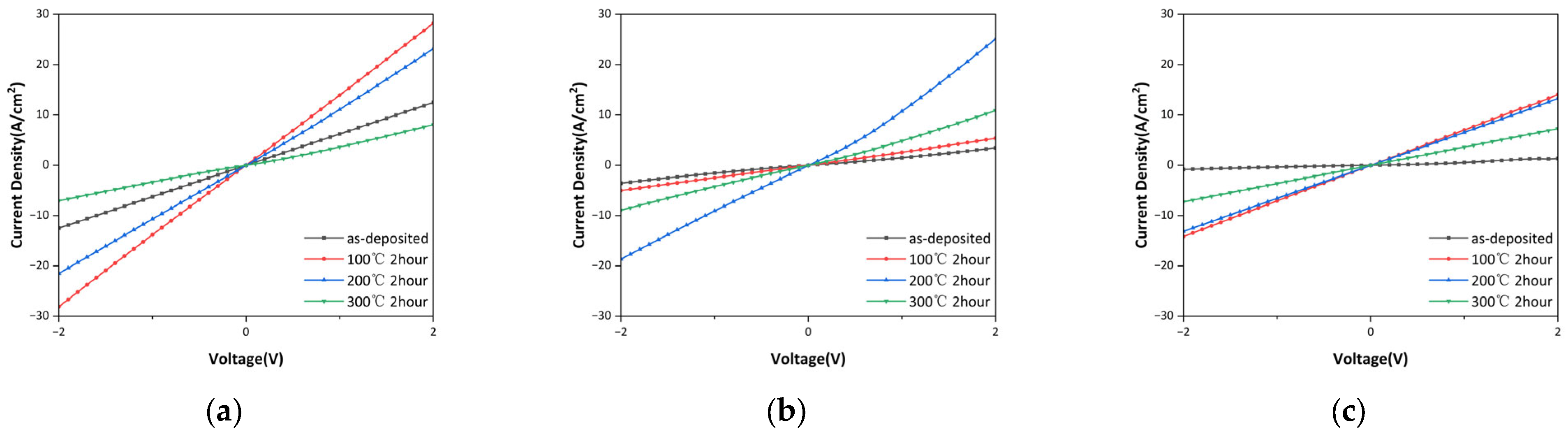
Figure 3 presents the linear-scale I-V characteristics for individual metal schemes under various thermal stress conditions, with each subplot dedicated to a single metallization system to track temperature-dependent degradation trends.
NiCuAl System. As shown in
Figure 3a, the as-deposited NiCuAl sample exhibited moderate forward conduction. After annealing at 100 °C for 2 h, the device demonstrated significantly enhanced forward current density, reaching over 25 A/cm
2 at 2 V, indicating the formation of improved ohmic contact at the Ni/ITO/p-GaN interface. However, further increasing the annealing temperature to 200 °C resulted in slight degradation of forward characteristics, and dramatic deterioration occurred at 300 °C, where the forward current density dropped below 10 A/cm
2 at 2 V. This pronounced thermal sensitivity suggests that Ni provides limited blocking effectiveness against Cu diffusion at elevated temperatures.
TiCuAl System.
Figure 3b reveals distinct behavior for the TiCuAl configuration. The as-deposited sample showed relatively poor forward conduction compared to NiCuAl, with higher series resistance. Upon 100 °C annealing, modest improvement was observed, while the optimal electrical performance was achieved at 200 °C, with forward current density exceeding 20 A/cm
2 at 2 V. Notably, even after 300 °C annealing, the TiCuAl device maintained reasonable forward conduction, with current density approximately 10 A/cm
2 at 2 V, substantially superior to the NiCuAl counterpart under identical thermal stress. This indicates that Ti forms more effective interfacial barriers against Cu diffusion than Ni.
PtCuAl System. As depicted in
Figure 3c, the PtCuAl system exhibited the highest thermal stability among the three configurations. The as-deposited sample showed the poorest initial forward conduction, consistent with the chemically inert nature of Pt requiring thermal activation for interface reaction. Progressive improvement was observed with increasing annealing temperature, with the 200 °C and 300 °C samples demonstrating comparable and optimal forward characteristics. The PtCuAl device annealed at 300 °C exhibited moderate electrical degradation compared to its 100 °C and 200 °C counterparts, as evidenced by reduced forward current density at 2 V (
Figure 3c). Nevertheless, this degradation was substantially less severe than the catastrophic failure observed in NiCuAl at equivalent thermal stress, supporting Pt’s superior chemical stability as a Cu diffusion barrier.
Series resistance (R
s) shown in
Table 1 was extracted from the linear region of the I–V curves in the forward-bias range of 0 to 0.2 V, where the I–V relationship is approximately linear. A linear fit (
) was applied to this region, and the slope of the fit was taken as the series resistance. The extracted series resistance values exhibit distinct trends across the three metallization schemes. For NiCuAl, the series resistance increases dramatically to 0.1356 Ω after 300 °C annealing, which is more than three times the as-deposited value, indicating severe degradation of the contact and bulk conductivity due to Cu diffusion. In contrast, TiCuAl shows excellent thermal stability: the series resistance remains nearly constant (0.0423 Ω as-deposited vs. 0.0457 Ω at 300 °C), with a slight decrease after 200 °C annealing (0.0360 Ω) that correlates with the formation of Ti–Cu intermetallic compounds and improved ohmic contact. PtCuAl also demonstrates stable series resistance across all temperatures, varying between 0.0338 Ω and 0.0653 Ω, with no catastrophic increase at 300 °C.
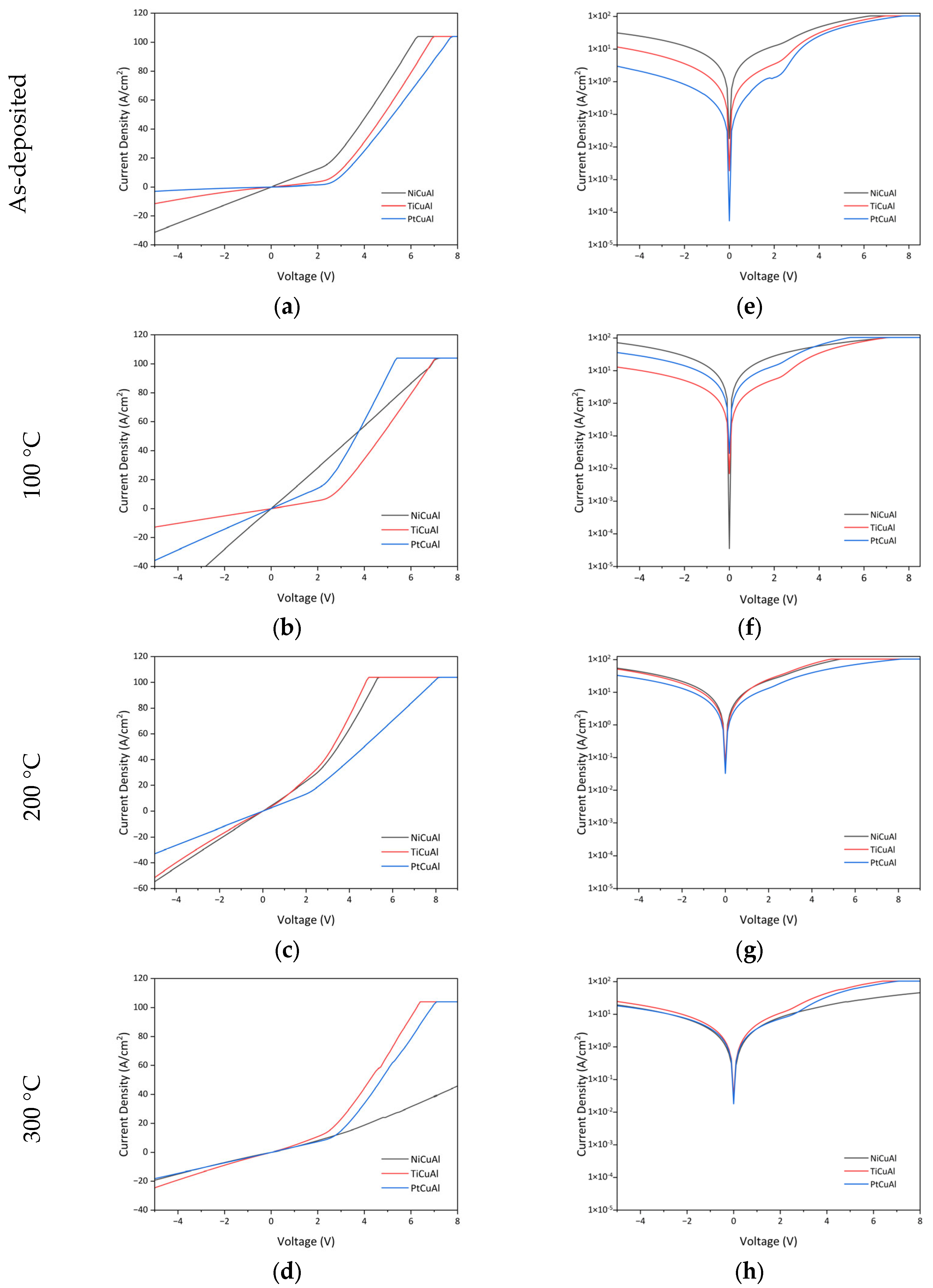
Figure 4 presents a comprehensive comparison of the three metal systems under identical annealing conditions, enabling direct assessment of barrier metal effectiveness. In the as-deposited state (
Figure 4a,e), NiCuAl demonstrates the best forward conduction due to favorable initial interface properties between Ni and ITO, while PtCuAl exhibits the highest resistance requiring thermal activation. At 100 °C (
Figure 4b,f), NiCuAl achieves peak performance with the highest forward current density, whereas TiCuAl and PtCuAl show only moderate improvement, indicating their need for higher activation temperatures. At 200 °C (
Figure 4c,g), TiCuAl surpasses NiCuAl in forward current density, while NiCuAl begins to degrade, revealing the onset of Cu penetration through the Ni barrier. At 300 °C (
Figure 4d,h), the divergence becomes dramatic: NiCuAl exhibits severe degradation with current saturation at low voltages, TiCuAl maintains moderate performance with noticeable series resistance increase, and PtCuAl retains nearly optimal characteristics with minimal degradation. This systematic comparison establishes the barrier effectiveness hierarchy as Ti ≈ Pt >> Ni for the 300 °C thermal budget investigated. While Pt demonstrates marginally superior thermal stability with minimal electrical degradation, Ti achieves optimal balance between barrier performance and contact resistance optimization. Both metals significantly outperform Ni, which exhibits significant degradation above 100 °C and catastrophic failure at 300 °C. The critical temperature thresholds of ~250 °C for Ti and >300 °C for Pt determine practical processing windows for high-reliability applications.
3.2. Electroluminescence Characteristics and Optical Performance
The electroluminescence (EL) properties of the MicroLED devices were characterized under constant current injection to evaluate the influence of Cu diffusion on radiative recombination efficiency. All EL measurements were conducted at a fixed injection current density of 20 A/cm
2, ensuring consistent carrier injection levels for direct comparison across different metallization schemes and thermal treatments.
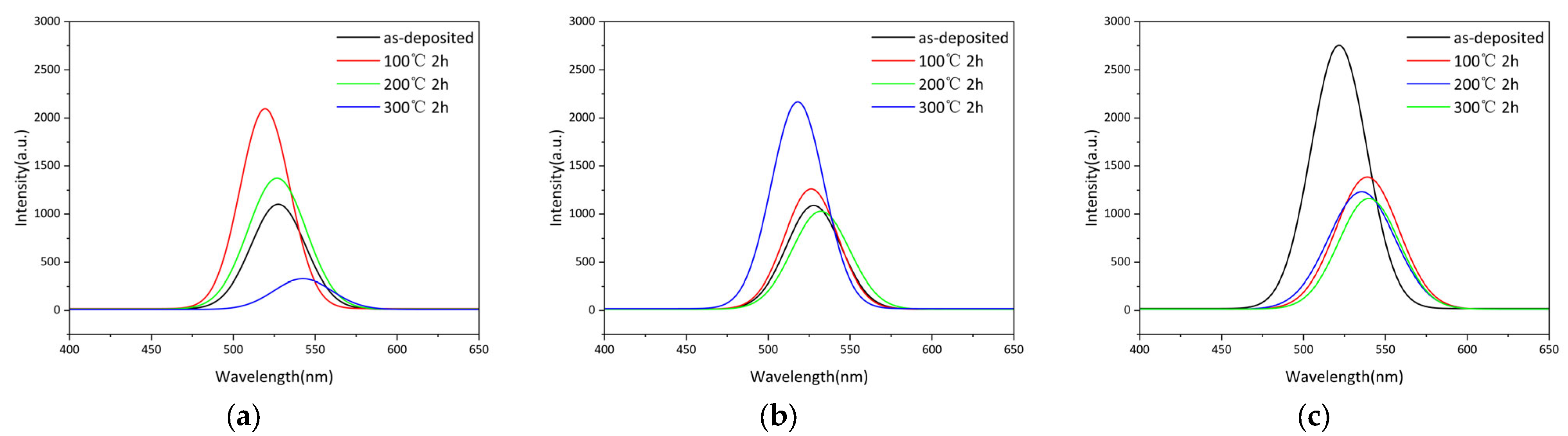
Figure 5 presents the normalized EL spectra for the three metal systems under various annealing conditions.
NiCuAl System—Severe Thermal Quenching. As shown in
Figure 5a, the NiCuAl device exhibited strong green emission centered at approximately 525 nm (2.36 eV) corresponding to the InGaN/GaN MQW transition. The as-deposited sample demonstrated moderate EL intensity of approximately 1100 arbitrary units (a.u.) at 20 A/cm
2. Annealing at 100 °C significantly enhanced the EL intensity to 2100 a.u., consistent with the improved carrier injection efficiency observed in I-V characteristics. However, further temperature increase resulted in progressive degradation, with samples annealed at 200 °C showing reduced intensity (~1350 a.u.) and samples annealed at 300 °C exhibiting dramatic quenching to merely 350 a.u.—corresponding to an 83% reduction compared to the optimal condition. Notably, the 300 °C spectrum exhibited significant spectral broadening (FWHM increased from ~39.2 nm to ~42.0 nm) and a clear red-shift of approximately 13.6 nm (from ~527.4 nm to ~541.0 nm), indicating potential damage to the quantum well structure and altered carrier distribution.
TiCuAl System—Thermal Enhancement of Performance.
Figure 5b reveals that the TiCuAl system exhibits a progressive increase in EL intensity with annealing temperature under 20 A/cm
2 injection. The as-deposited sample shows the lowest intensity, the 100 °C and 200 °C samples display moderate and comparable intensities (with 200 °C slightly lower than 100 °C), and notably, the sample annealed at 300 °C achieves the highest EL intensity among all TiCuAl devices. This temperature-dependent enhancement indicates that the Ti barrier remains effective in blocking Cu diffusion even at 300 °C, and that higher-temperature annealing further improves the ohmic contact, thereby increasing radiative recombination efficiency. In contrast to the catastrophic failure of NiCuAl at 300 °C, TiCuAl shows no degradation but rather improvement. The spectral peak wavelength remains within 526–532 nm for as-deposited, 100 °C, and 200 °C samples, with a slight blue shift to 518 nm at 300 °C, while the FWHM is consistently around 25 nm, supporting structural integrity preservation.
PtCuAl System—Anomalous Carrier Localization Effect. The PtCuAl system exhibited distinctly different behavior, as shown in
Figure 5c. Surprisingly, the as-deposited sample demonstrated the highest EL intensity of 2750 a.u. among all experimental conditions at 20 A/cm
2, despite possessing the poorest electrical conductivity. This apparent contradiction suggests the presence of carrier localization effects: the high contact resistance associated with the unannealed Pt/ITO/p-GaN interface restricts carrier injection to localized regions with potentially lower defect density, thereby enhancing the internal quantum efficiency. Annealing at 100 °C and 200 °C resulted in reduced EL intensities (1350 a.u. and 1200 a.u., respectively), possibly due to expanded carrier distribution exposing more non-radiative recombination centers. However, the sample annealed at 300 °C maintained 1150 a.u., representing the highest absolute EL intensity (1150 a.u.) among all samples annealed at 300 °C, while retaining 42% of its initial value.
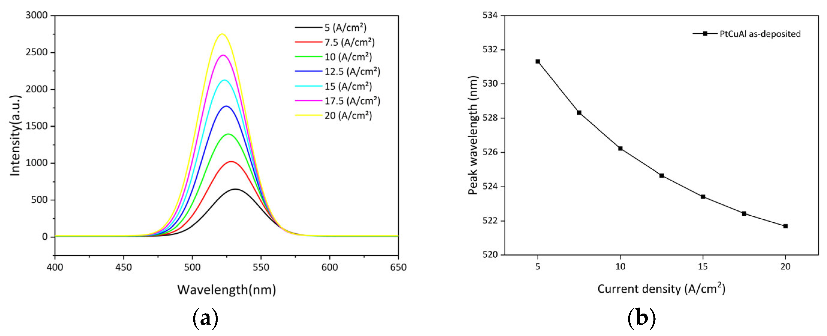
To further investigate the origin of the unexpectedly high EL intensity in the as-deposited PtCuAl device, we measured EL spectra at various injection current densities (5–20 A/cm
2), as shown in
Figure 6a. With increasing current density, the EL peak exhibits a gradual blue shift from 531.3 nm at 5 A/cm
2 to 521.6 nm at 20 A/cm
2, i.e., a total shift of ~10 nm (
Figure 6b). Such a blue shift is characteristic of the sequential filling of localized states in InGaN/GaN quantum wells: at low injection, carriers preferentially occupy lower-energy localized tail states; as the current increases, these states become saturated and carriers begin to recombine from higher-energy delocalized or weakly localized states, causing the emission to blue-shift. This behavior, together with the fact that the as-deposited PtCuAl device exhibits the poorest electrical conductivity yet the highest EL intensity, supports the carrier localization effect.
The integrated EL intensity as a function of injection current density (L-I characteristics) was analyzed to establish the relationship between electrical transport and optical efficiency. For NiCuAl and TiCuAl systems, the L-I characteristics demonstrated strong correlation with I-V behavior: samples with lower series resistance and higher forward current exhibited superior light extraction efficiency at equivalent injection levels. The external quantum efficiency (EQE), calculated from the ratio of emitted photons to injected electrons at 20 A/cm2, peaked at 100 °C for NiCuAl (~8.5%) and at 300 °C for TiCuAl (~9.2%), respectively. The PtCuAl system, however, exhibited anomalous L-I behavior: despite higher operating voltages required to achieve 20 A/cm2 injection, the as-deposited PtCuAl device demonstrated EQE of approximately 11.2%—significantly exceeding the annealed counterparts, attributed to the aforementioned carrier localization effect.
3.3. SIMS Analysis of Cu Diffusion Profiles
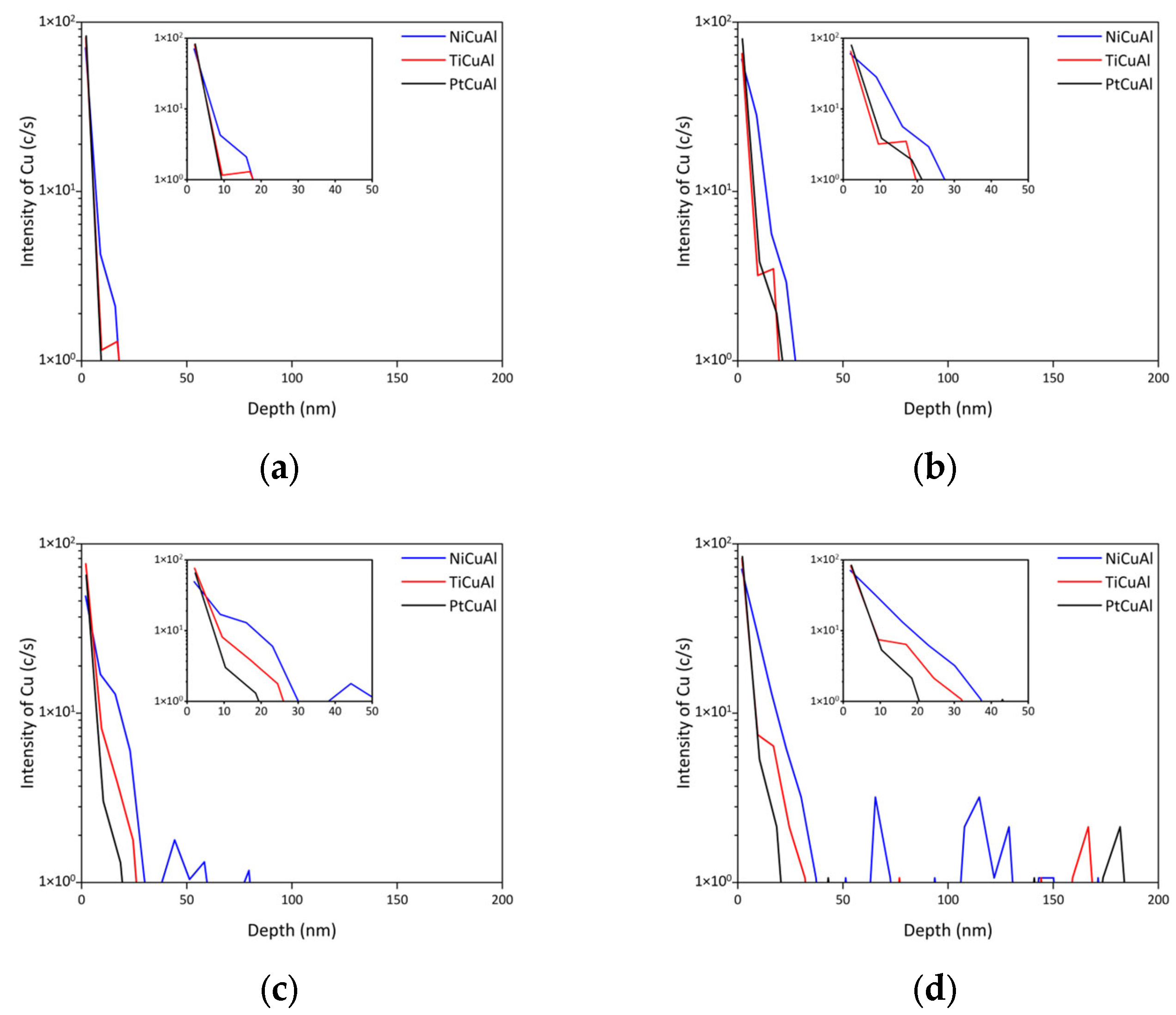
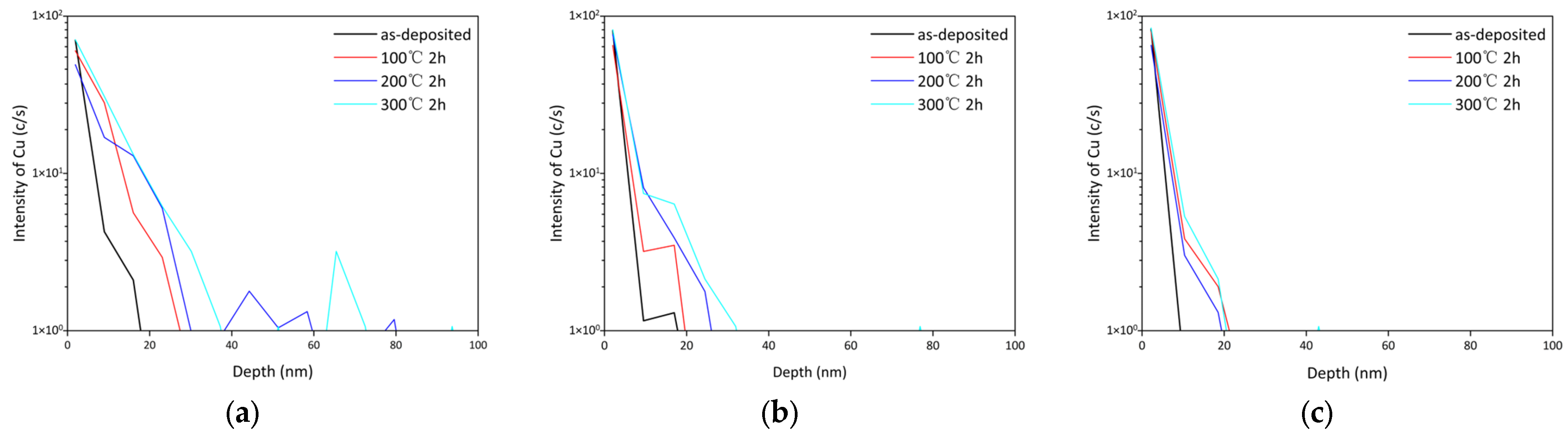
To directly confirm that the observed electrical and optical degradation originates from Cu penetration into the semiconductor, SIMS was performed on selected samples after complete removal of the surface metal stack. Thus, the measured Cu signal originates solely from Cu atoms that have diffused through the barrier metal layer and entered the underlying p-GaN. Two complementary comparisons are presented: (i) across different metallization schemes under the same annealing condition (
Figure 7), and (ii) across annealing temperatures for each metallization scheme (
Figure 8). The Cu secondary ion intensity (counts/s) is a semi-quantitative measure of relative Cu concentration in GaN, with depth scale calibrated by profilometry.
For the as-deposited NiCuAl sample (
Figure 8a), after metal removal, the Cu signal in GaN is near the detection limit, indicating no detectable Cu diffusion. After annealing at 100 °C, a very weak Cu signal appears in the near-surface region of GaN, consistent with the onset of Cu penetration through the Ni barrier. At 200 °C, a clear Cu tail is observed extending to a depth of ~100 nm into GaN. At 300 °C, the Cu signal becomes strongly elevated and remains high throughout the entire analyzed depth (exceeding 200 nm), demonstrating that Cu has massively diffused into the p-GaN and likely reached the MQW region. This correlates directly with the catastrophic electrical degradation (
Figure 3a) and 83% EL quenching (
Figure 5a) at 300 °C.
After metal removal, the as-deposited TiCuAl samples and those annealed at 100 °C (
Figure 8b) show no measurable Cu in GaN. At 200 °C, a very weak Cu signal appears only in the first 20 nm of GaN, indicating that the Ti-Cu intermetallic barrier (TiCu, Ti
2Cu, TiCu
4) remains largely intact. Even at 300 °C, the Cu concentration in GaN is substantially lower than that in the NiCuAl counterpart (
Figure 7d), consistent with the much weaker SIMS signal, and the Cu profile is confined to the near-surface region (<50 nm). This limited Cu penetration explains why TiCuAl retains moderate forward conduction (
Figure 3b) and 47% of its peak EL intensity (
Figure 5b) even after 300 °C annealing.
Across all annealing temperatures (up to 300 °C), the Cu signal in GaN after metal removal for PtCuAl system (
Figure 8c) remains at the background level, with no detectable tail. This unequivocally proves that Pt is an exceptionally effective diffusion barrier, preventing Cu from entering the GaN lattice under the investigated thermal budgets. The mild performance degradation observed for PtCuAl at 300 °C may be due to residual defects in the Pt layer (e.g., pinholes or grain boundaries) or interfacial reactions, which require further investigation.
After 300 °C annealing and metal removal, the three metallizations (
Figure 7d) show a clear hierarchy of Cu penetration into GaN: NiCuAl exhibits a strong, deep Cu signal; TiCuAl shows a weak, shallow Cu signal; PtCuAl displays no detectable Cu. This ranking matches the barrier effectiveness deduced from electrical and optical measurements and provides direct experimental evidence that Cu diffusion into GaN is the primary cause of device degradation at elevated temperatures.
The SIMS results quantitatively explain the temperature-dependent failure modes: (i) NiCuAl fails above 100 °C because Cu rapidly interdiffuses with the Ni layer (complete solid solution) and penetrates into GaN; (ii) TiCuAl performs optimally at 200 °C (minimal Cu in GaN) and shows only limited Cu penetration at 300 °C, thanks to the formation of stable intermetallic compounds; (iii) PtCuAl exhibits no detectable Cu in GaN even at 300 °C, confirming its superior barrier integrity. These findings establish that the barrier metal choice dictates Cu diffusion kinetics into the semiconductor and ultimately determines the thermal reliability of GaN-based devices.
4. Discussion
The comprehensive analysis of electrical and optical data enables quantitative assessment of Cu diffusion behavior and the effectiveness of different barrier metals. The degradation of device performance at elevated temperatures directly correlates with Cu penetration depth into the semiconductor structure.
The rapid performance degradation of NiCuAl devices above 100 °C indicates insufficient barrier effectiveness. Ni and Cu form complete solid solutions with mutual diffusivity estimated to exceed 10
−14 cm
2/s at 300 °C [
16]. The interdiffusion creates Ni-Cu alloy phases that compromise the original barrier integrity, enabling Cu penetration through the 10 nm Ni layer into the underlying ITO and p-GaN. The EL quenching at 300 °C under 20 A/cm
2 injection suggests Cu reaching the MQW region, where Cu incorporation introduces deep-level non-radiative recombination centers, drastically reducing carrier lifetime and radiative efficiency.
Ti demonstrates superior barrier performance due to the formation of intermetallic compounds (TiCu, Ti
2Cu, TiCu
4) at the Ti-Cu interface [
17], which present higher activation energy for Cu diffusion compared to Ni-Cu alloys. The optimal performance window at 200 °C corresponds to the completion of interface reaction while maintaining barrier integrity. At 300 °C, partial barrier degradation occurs through Cu penetration along grain boundaries or localized diffusion pathways, resulting in moderate but non-catastrophic device degradation.
Pt exhibits the highest chemical stability and lowest mutual diffusivity with Cu among the three systems. The Pt-Cu system requires temperatures exceeding 400 °C for significant interdiffusion, rendering the 300 °C annealing condition insufficient for complete barrier breakdown. The observed performance degradation in PtCuAl devices at elevated temperatures is attributed primarily to Cu diffusion through localized defects or pinholes in the Pt layer rather than bulk diffusion, preserving overall device functionality.
The correlation between I-V and EL degradation patterns reveals distinct mechanisms governing electrical and optical performance. The increase in series resistance and ideality factor at elevated temperatures primarily stems from: Cu-induced acceptor compensation in p-GaN, reducing hole concentration and increasing resistivity; formation of Cu-related deep levels near the interface, enhancing tunneling-assisted recombination and increasing non-ideal current components; possible oxidation or phase transformation at the metal/ITO interface increasing contact resistance.
The EL intensity reduction at 20 A/cm2 follows more complex pathways: Cu reaching the MQW region introduces non-radiative recombination centers, reducing internal quantum efficiency through Shockley–Read–Hall recombination; Cu-induced strain or interdiffusion at InGaN/GaN interfaces modifies quantum confinement and transition probabilities; carrier leakage enhancement due to modified band alignment and defect-assisted tunneling occurs; for NiCuAl at 300 °C, possible formation of metallic precipitates or conductive paths occurs, causing local short-circuits and current crowding.
This systematic investigation of Cu diffusion effects in GaN-based devices with NiCuAl, TiCuAl, and PtCuAl electrode systems reveals that Cu diffusion poses critical reliability threats to MicroLED performance, with degradation onset temperatures varying significantly based on barrier metal selection: Ni (~100 °C), Ti (~200–250 °C), and Pt (>300 °C). Notably, Ti achieves optimal performance at 200 °C, whereas Pt maintains stability across the entire investigated temperature range. The comparative analysis establishes a clear hierarchy of barrier effectiveness as Ti ≈ Pt >> Ni, with Pt demonstrating marginally superior thermal stability and Ti achieving optimal peak performance. TiCuAl provides the optimal general-purpose solution, achieving peak electroluminescence intensity of 2150 a.u. at 20 A/cm2 with 200 °C annealing, balanced electrical and optical characteristics, and maintaining reasonable performance at 300 °C; PtCuAl offers superior thermal stability and reveals unexpected carrier localization effects in unannealed devices, suggesting opportunities for efficiency optimization through contact engineering; NiCuAl is suitable only for low-temperature applications (≤100 °C), with rapid performance degradation above this threshold due to insufficient Cu blocking effectiveness; optical characterization at fixed injection density serves as a more sensitive indicator of Cu diffusion to the active region than electrical measurements alone, highlighting the importance of combined electro-optical analysis for reliability assessment.
These findings establish fundamental guidelines for electrode metallization design in MicroLED technology and contribute to the understanding of metal–semiconductor interaction mechanisms in III-nitride optoelectronic devices.
The barrier effectiveness hierarchy established here for 350 μm-diameter devices is expected to be even more critical for smaller pixel sizes (e.g., <10 μm) due to the higher perimeter-to-area ratio, which provides more diffusion pathways along sidewall defects. Additionally, the emission wavelength may influence Cu diffusion through its effect on the internal electric field and quantum well strain. For shorter-wavelength (e.g., blue or UV) devices with higher Al content, the diffusion behavior could differ; this remains an open question for future study.
5. Conclusions
This study systematically investigated the influence of Cu diffusion on the electrical and optical performance of GaN-based light-emitting devices with three barrier metallization schemes (NiCuAl, TiCuAl, PtCuAl) under thermal annealing up to 300 °C. The key findings are summarized as follows:
Barrier effectiveness hierarchy: Ti and Pt both significantly outperform Ni in blocking Cu diffusion. NiCuAl devices suffer catastrophic degradation above 100 °C (83% EL quenching at 300 °C), whereas TiCuAl and PtCuAl maintain good performance even at 300 °C.
Optimal general-purpose barrier: TiCuAl exhibits increasing EL intensity with annealing temperature, achieving its highest emission at 300 °C without any sign of Cu-induced degradation. This indicates that Ti effectively blocks Cu diffusion while thermal activation progressively improves contact performance. Ti is therefore the most suitable barrier metal for mainstream high-performance applications requiring processing up to 300 °C.
Best thermal stability: PtCuAl exhibits no detectable Cu diffusion into GaN even at 300 °C, retaining 42% of its as-deposited EL intensity. Pt is therefore preferred for extreme reliability requirements or high-temperature processing (>300 °C), despite higher material cost.
In summary, Ti is recommended as the optimal general-purpose Cu diffusion barrier for GaN-based LEDs, while Pt is the choice for ultimate thermal stability. Ni should be avoided for applications exceeding 100 °C. These findings provide practical design guidelines for electrode metallization in high-reliability GaN optoelectronic devices.