


Abstract
Amorphous gallium oxide thin-film transistor photodetectors are promising for ultraviolet detection because of their wide bandgap and low dark current. Magnetron sputtering is compatible with low-temperature processing, but device performance is sensitive to sputtering conditions. Poor parameter choices can introduce oxygen vacancies and interface charges, degrading optoelectronic performance. Here, a three-factor, three-level orthogonal design is used to vary sputtering power, Ar/O2 flow ratio, and film thickness. Nine device sets are fabricated and compared based on transfer characteristics and transient photocurrent–time (I-t) responses measured at a wavelength of 254 nm, with clear differences observed among process combinations. To identify the origin of these differences, representative samples with significant responsivity variations were modeled using TCAD. By fitting the simulated I-t curves to measured transients, the interface fixed charge density and defect-state densities were extracted, and the photon absorption distribution of different samples was analyzed. This analysis, from both defect and UV absorption perspectives, revealed the reasons for the differences in responsivity. The absorption coefficients at 254 nm measured by ellipsometry for the two samples were also compared, and the absorption trends observed in both the simulation and ellipsometry were consistent, confirming the accuracy of the simulation results. This work presents an integrated experimental and TCAD approach for process optimization and mechanistic analysis of a-GaOx TFT-PDs.
1. Introduction
Ultraviolet (UV) detection technologies are important for applications such as environmental monitoring, space exploration, and secure communications. The solar-blind band (200–280 nm) has a very low terrestrial background because atmospheric ozone strongly absorbs these wavelengths, which supports low-noise UV detection with a high signal-to-noise ratio [1,2,3,4]. Among solar-blind UV detector architectures, thin-film transistor photodetectors (TFT-PDs) integrate photodetection with gate-controlled amplification, enabling tunable responsivity magnitude and the operating window through gate bias, while also offering advantages in low power consumption and straightforward array-level integration [5,6,7]. Amorphous gallium oxide (a-GaOx) exhibits a wide intrinsic bandgap, which enables a-GaOx TFT-PDs to achieve inherently low dark current and high UV sensitivity, making it an attractive channel material for solar-blind UV photodetectors [8,9,10]. However, a-GaOx films are typically fabricated by low-thermal-budget processes like magnetron sputtering, where deposition parameters (e.g., sputtering power, Ar/O2 gas flow ratio, and thickness) affect film densification, oxygen-related defects, and interface charge states, which ultimately determine the device performance, including dark current, responsivity amplitude, and transient response [11,12,13]. Thus, an efficient experimental design is needed to optimize these key parameters and identify the primary causes of performance variation.
In studies of TFT-PDs, device performance is sensitive to both the channel material and the deposition process. Many studies adopt a one-factor-at-a-time approach, where composition, doping level, channel thickness, or ambient conditions are varied individually to evaluate their effects on optoelectronic performance [14,15,16,17,18,19]. This approach is useful for identifying the effect of a single factor, but it is less effective for a-GaOx sputtering because sputtering power, Ar/O2 gas flow ratio, and film thickness influence film densification, defect formation, and interface charge states at the same time and jointly determine dark current, responsivity amplitude, and transient behavior. Under such coupled effects, one-factor scanning requires many repeated experiments to cover different combinations and often produces fragmented conclusions, so the relative contributions of each factor are difficult to compare within one framework. Orthogonal experimental design addresses this issue by evaluating multiple factors in a limited set of experiments and enabling rapid identification of sensitive ranges and near-optimal combinations. Accordingly, this work employed a three-factor, three-level orthogonal design to vary sputtering power, Ar/O2 gas flow ratio, and film thickness, and the resulting devices were compared using transfer characteristics and 254 nm transient photocurrent responses. This design provides the basis for subsequent main-effect analysis and mechanistic discussion.
In TFT-PD research, technology computer-aided design (TCAD) and related numerical simulations are instrumental for analyzing device physics, optimizing structures, and attributing performance variations to device-level factors like defect states, interface charges, and optical absorption. Prior work can be grouped into three types. First, mechanism-oriented simulations model band structure, electric fields, and carrier distributions before and after illumination to elucidate photocarrier generation and transport [20,21,22]. For example, Vidal Lorbada et al. (2020) [20] attributed the phototransistor-like behavior of Copper Indium Gallium Selenide devices to the back-contact barrier. They reported that, after bias treatment at ±0.4 V and 100 °C for 16 h, forward bias reduced the apparent barrier height from ~340 meV to ~290 meV and strongly modulated the photocurrent response [20]. Second, structure-optimization simulations systematically explore geometric or material parameters such as doping concentration, channel thickness, and junction dimensions to evaluate their impact on device performance, thereby guiding device optimization [18,23,24]. Yoon et al. used TCAD to study Sn-doped β-Ga2O3 phototransistors by fitting dark transfer characteristics and analyzing the transition between depletion-mode and enhancement-mode operation; they found that a thinner channel reduced power consumption and shortened response time but at the cost of responsivity (R), specific detectivity (D*), and external quantum efficiency (EQE) which improved with a thicker channel, indicating a trade-off between response speed and detection figures of merit [18]. Similarly, Kim et al. simulated lateral p-n-i-p-n phototransistor arrays and optimized pixel structures by varying Si active-layer thickness and doping. They found reducing the active-layer thickness suppressed dark current and improved the usable dynamic range [23]. Third, structure-innovation and feasibility-validation simulations assess emerging architectures such as heterojunction devices and avalanche phototransistors [25,26,27,28,29]. Gao et al. combined photocurrent mapping with TCAD simulations in an Au-WSe2-Ge separate-absorption-and-multiplication (SAM) phototransistor. They demonstrated that carrier multiplication mainly occurred at the Au/WSe2 Schottky junction, while near-infrared absorption mainly originated from the WSe2/Ge heterojunction, supporting the SAM concept [25]. Su et al. used TCAD in an all-GaN UV phototransistor-micro-LED platform and optimized epitaxial-layer thickness and doping, confirming optical driving and modulation in the integrated structure [26]. Overall, these three types emphasize different goals including mechanistic analysis, experimental optimization, and structure exploration.
TCAD and numerical simulations are widely used to study device mechanisms and evaluate phototransistor structures, but integration with experimental results remains limited. In many studies, simulations reproduce electrical characteristics by fitting dark-state transfer (ID-VG) curves, whereas experimental validation under illumination often focuses on confirming qualitative trends. As a result, simulations frequently rely on preset material and defect parameters to illustrate specific physical effects or predict performance variations. Quantitative fitting of experimental response curves—especially transient photocurrent–time (I-t) behaviors—remains relatively scarce, even though it can extract defect- and interface-related parameters and enable device-level comparisons among samples fabricated under different process conditions.
While the threshold voltage is a useful descriptor of the dark transfer characteristic and is often correlated with defect-related effects, it cannot uniquely separate the contributions from interface fixed charge, bulk trapping, and optical generation, nor does it capture the transient trapping/detrapping dynamics that govern the photoresponse under UV illumination. These limitations motivate the use of a more comprehensive, physics-based approach. Therefore, we selected representative samples with clearly different responsivity based on experimental results and constructed corresponding TCAD models using the same device geometry, bias conditions, and illumination settings as in the measurements. By fitting the simulated I-t response curves to the measured transients, we extracted key parameters, including the interface fixed charge density and sub-gap defect-state densities, and further interpreted the differences in responsivity amplitude and transient dynamics by analyzing the spatial distribution of photon absorption rate. With this workflow, the simulations reproduced the experimental observations and yielded a consistent set of extracted parameters that reflect process-induced variations in material and interface quality, thereby providing mechanistic insights for device-level interpretation.
In this work, a three-factor, three-level orthogonal design is used to evaluate the effects of sputtering power, Ar/O2 flow ratio, and film thickness on device performance. Representative samples are then selected for TCAD analysis, from which interface fixed charge density and defect-state parameters are extracted and compared. Finally, spectroscopic ellipsometry is performed to measure the absorption coefficient at 254 nm and to cross-check the simulated absorption trends. The consistency between simulation and ellipsometry further supports the reliability of the TCAD model. Overall, this work presents an integrated experimental simulation methodology for process optimization and mechanistic analysis of performance differences in a-GaOx TFT-PDs.
2. Materials and Methods
2.1. Film Deposition and Device Fabrication
Bottom-gate a-GaOx TFT-PDs were fabricated. Commercial p+-Si/SiO2 wafers were used as substrates, where heavily doped p-type Si served as the bottom gate electrode and thermally grown SiO2 (100 nm) acted as the gate dielectric. The a-GaOx semiconductor layer was deposited by radio-frequency (RF) magnetron sputtering from a Ga2O3 ceramic target at room temperature in an Ar/O2 mixed atmosphere. To systematically evaluate the effects of sputtering parameters on film quality and device performance while minimizing the number of experimental runs, a three-factor, three-level orthogonal design was adopted. Three key factors, namely, sputtering power, Ar/O2 gas flow ratio, and film thickness (target levels of 20, 30, and 40 nm), were set at three levels. The corresponding sputtering conditions and measured film thickness values are listed in Table 1. Film thickness was controlled by deposition time and was measured by spectroscopic ellipsometry after deposition; each sample was measured three times under identical conditions, and the thickness was reported as mean ± standard deviation (n = 3). All other fabrication steps were kept identical. The semiconductor channel and source/drain regions were defined using a metal shadow mask, with a channel length and width of 400 μm and 800 μm, respectively. Aluminum (Al) was employed as the source/drain electrode material and was deposited by direct-current (DC) magnetron sputtering through the shadow mask to form a parallel-electrode configuration with a thickness of approximately 100 nm. After completing device fabrication, a post-annealing treatment was performed at 400 °C under vacuum for 60 min.
Table 1.
Sputtering conditions and film thickness for each orthogonal experimental group.
2.2. Device Characterization and TCAD Simulation
Electrical and responsivity measurements were performed using a semiconductor parameter analyzer (4200 SCS, Keithley, Cleveland, USA), and illumination was provided by a monochromator (Omni-λ 3007, Horiba Scientific, Kyoto, Japan). Device optoelectronic performance was evaluated by measuring transfer characteristics and transient I-t responses under 254 nm illumination with a power density of 0.741 µW∙cm−2. The optical properties of the films were characterized using a variable-angle spectroscopic ellipsometer (M-2000DI, J. A. Woollam, Lincoln, NE, USA). The measurements covered the ultraviolet-to-near-infrared spectral range (240–1700 nm). Film thickness, refractive index, and absorption coefficient were extracted to evaluate optical absorption under different processing conditions. Spectroscopic ellipsometry was performed on Si substrates coated in the same sputtering conditions as the devices. For ultrathin films (20–40 nm), ellipsometric fitting could suffer from correlations between thickness and optical constants. To reduce this ambiguity, the Ψ and Δ spectra were fitted using a physically constrained air/a-GaOx/Si model, where the Si optical constants were taken from the software library and kept fixed. The a-GaOx layer was described using a Tauc–Lorentz dispersion model (Gen-Osc). The final fits showed good agreement between the measured and fitted Ψ and Δ spectra. Representative Ψ and Δ spectra together with the fitted curves for the S4 and S7 films were provided in Appendix A (Figure A1). In addition, an ellipsometric uniqueness verification was conducted by examining the stability of the fitting solution against parameter perturbation and by checking the mean squared error (MSE) landscape, indicating that the extracted parameters were stable and well constrained. Each film was measured three times under identical conditions, and the thickness was reported as mean ± standard deviation (n = 3).
TCAD simulations used a bottom-gate device model consistent with the experimental structure, including a Si bottom gate, a SiO2 gate dielectric, an a-GaOx channel layer, and source/drain electrodes. All simulations shared the same device geometry, boundary conditions, transport framework, and optical generation/absorption formalism to ensure a consistent comparison among samples. Within this unified setup, only parameters associated with material/interface quality were treated as sample-dependent and were extracted by fitting the measured transient I–t responses, including the interfacial fixed charge density (Qf) and the sub-gap defect-state parameters (NTA/NTD and NGA/NGD). All other material parameters were kept identical across samples. The a-GaOx layer was described using a wide-bandgap oxide model, and bulk trap states were introduced in the channel to capture defect states in amorphous oxides. Following widely used modeling practice for amorphous oxide semiconductors, band-tail states were represented by exponential distributions and deep states by Gaussian distributions; in TCAD these were parameterized by the tail-state densities (NTA/NTD) and deep-state densities (NGA/NGD) for acceptor-like and donor-like components, respectively [30,31,32]. Transient simulations were performed by switching the illumination intensity following a defined time sequence to generate I–t response curves. The illumination wavelength (254 nm) and time sequence were kept consistent with the experiments, and the absorption input at 254 nm was handled in the same manner across samples.
3. Results and Discussion
3.1. Comparison of Electrical and Responsivity Characteristics of Orthogonal-Design A-GaOx TFT-PDs
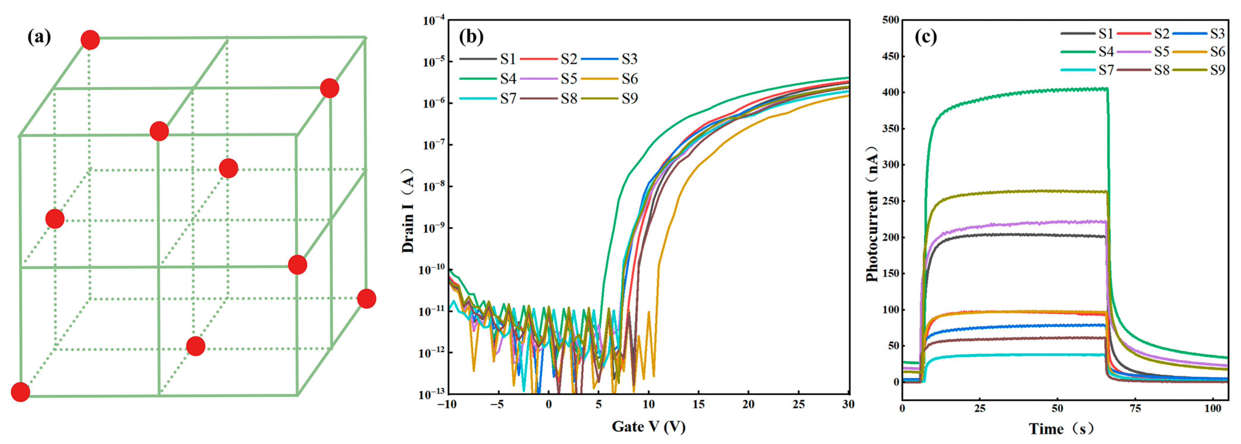
Figure 1 summarizes the key electrical and responsivity characteristics of the nine TFT-PDs fabricated based on the design matrix in Table 1. Figure 1a shows the factor-level combinations in the three-factor, three-level orthogonal design. Here, the orthogonal design matrix refers to a predefined experimental layout (e.g., an L9 array) that selects a small subset of experimental runs from all possible factor combinations while maintaining balanced and independent levels for each factor. Specifically, each level of sputtering power, Ar/O2 flow ratio, and the target film thickness (20, 30, and 40 nm) appears the same number of times across the nine runs, allowing efficient comparison of the main effects with significantly fewer experimental runs. This design ensures that the levels of each factor are evenly distributed, enabling effective evaluation of their influence on device performance while maintaining statistical integrity. These nine experimental points cover different combinations of the three key factors: sputtering power, Ar/O2 gas flow ratio, and film thickness. The orthogonal design systematically selects the experimental points, ensuring they are evenly distributed within the range of each factor, allowing us to effectively evaluate the influence of each factor with fewer experimental data. Figure 1b reveals distinct variations in the dark transfer characteristics among the orthogonal-design samples, indicating that sputtering conditions affect channel conduction in a-GaOx. Figure 1c presents the transient I-t curves under 254 nm UV illumination. The samples exhibit varying steady-state photocurrent levels and different rise/decay behaviors during light on/off switching. Electrical transfer parameters vary markedly under different process conditions, as summarized in Table 2. With increasing sputtering power, the subthreshold swing (SS) generally increases, which may be associated with an increased density of interface states and sub-gap defect states (e.g., tail states and deep-level states). The devices with a film thickness of 30 nm exhibit overall better electrical performance, featuring a smaller SS and a higher field-effect mobility (μFE); in contrast, the 20 nm and 40 nm groups show weaker electrical metrics, indicating that 30 nm is more favorable for achieving a balanced transfer behavior in terms of electrostatic control and carrier transport within the present window. Notably, S4 simultaneously shows the highest responsivity and the highest mobility, whereas S7 exhibits the lowest responsivity together with the lowest mobility. A detailed comparison and discussion of the photoelectrical metrics are presented in Section 3.2. Taken together, these results indicate that deposition conditions modulate channel conduction and interface-related effects, thereby influencing both the transfer characteristics and the overall photoelectrical performance.
Figure 1.
Orthogonal design matrix and the corresponding electrical and responsivity characteristics. (a) Factor-level combinations in the three-factor, three-level orthogonal design; (b) dark transfer curves of the a-GaOx TFT-PDs; (c) transient I-t curves measured under 254 nm illumination (power density: 0.741 µW∙cm−2) at VDS = 10.1 V. During the transient measurement, VGS is fixed at the turn-on voltage (VON) extracted from the dark transfer curve of each device.
Table 2.
Key electrical and responsivity parameters of a-GaOx TFT-PDs for different orthogonal-design samples.
3.2. Main-Effect Analysis of Magnetron Sputtering Parameters on the Responsivity of a-GaOx TFT-PDs
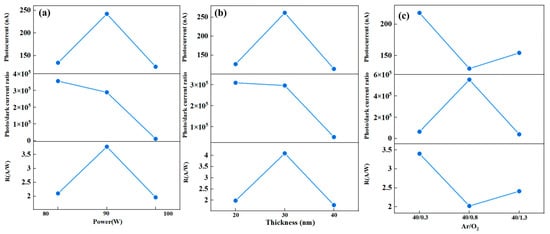
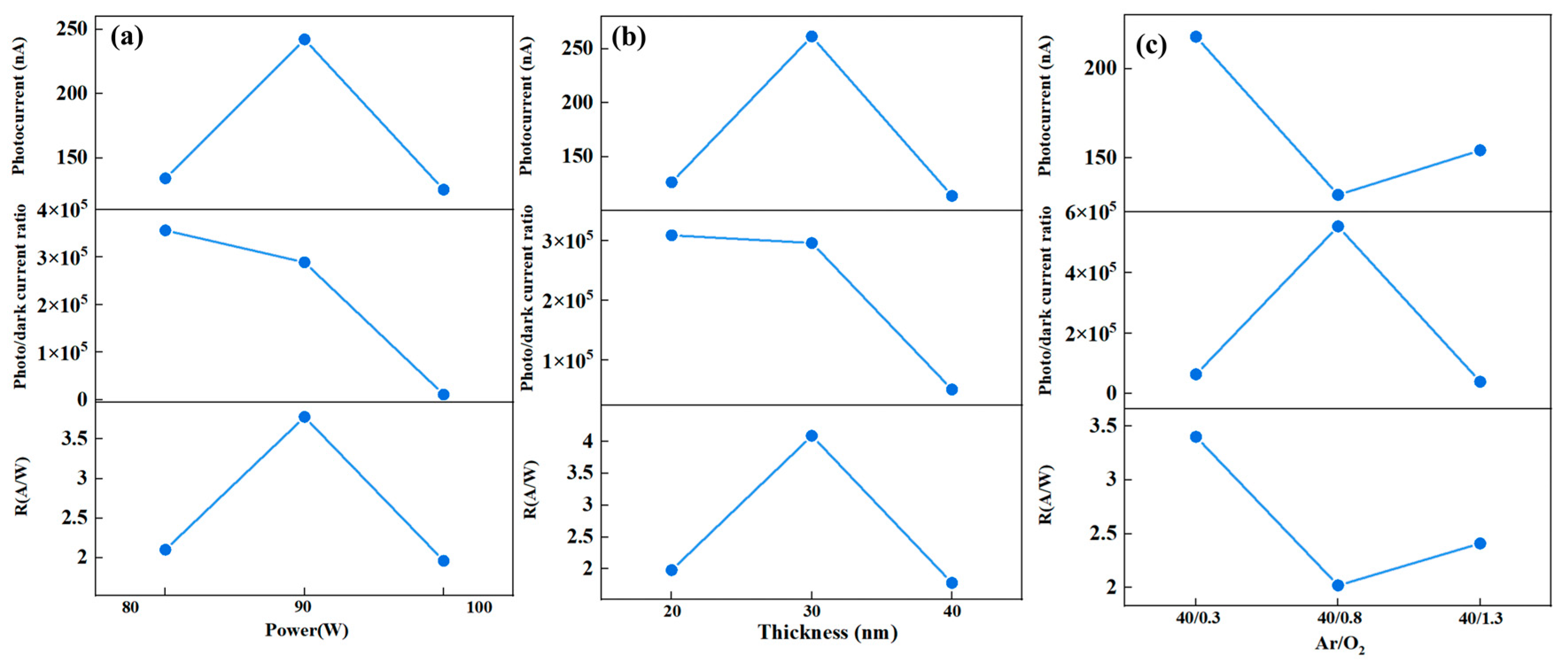
Based on the orthogonal results, we conduct a main-effect analysis of sputtering power, Ar/O2 flow ratio, and a-GaOx film thickness, as shown in Figure 2. Photocurrent and responsivity rise as the sputtering power increases from 80 W to 90 W, whereas both decrease dramatically when the power increases to 100 W in Figure 2a, suggesting an optimal power range around 90 W. The photo/dark current ratio decreases as power increases, which suggests that dark current rises faster than photocurrent at higher power.
Figure 2.
Main-effect analysis of magnetron sputtering parameters on the responsivity of a-GaOx TFT-PDs. (a) Sputtering power; (b) a-GaOx film thickness; (c) Ar/O2 flow ratio. From top to bottom, the metrics are photocurrent, photo/dark current ratio, and responsivity.
Figure 2b reveals that increasing the target thickness level from 20 nm to 30 nm improves photocurrent, photo/dark current ratio, and responsivity. However, a further increase to 40 nm reduces these metrics. This suggests that moderate thickness improves UV absorption while maintaining gate control and carrier collection. But an overly thick channel weakens gate control through the film and increases bulk trapping, which collectively limit photocarrier collection and elevate dark current. Figure 2c indicates that the Ar/O2 flow ratio affects device performance. The photocurrent and responsivity are highest at 40/0.3 sccm, lower at 40/0.8 sccm, and partially recover at 40/1.3 sccm. In contrast, the photo/dark current ratio peaks at 40/0.8 sccm. This trend can be understood in terms of oxygen incorporation during sputtering, which modulates oxygen-vacancy-related defects and sub-gap trap populations in the film and at the dielectric/channel interface. A lower O2 flow can increase donor-like oxygen vacancies, enhancing carrier density and photocurrent but also elevating the dark current, whereas an intermediate O2 level can better suppress the dark current by mitigating vacancy-related donor states and interfacial charge effects. These oxygen-incorporation effects are further quantified by the TCAD-extracted parameters in Section 3.3, including Qf and the sub-gap defect-state densities (NTA/NTD and NGA/NGD). The main-effect results suggest that the optimal process window is near 90 W sputtering power, 30 nm film thickness, and a low O2 flow ratio (40/0.3 sccm).
3.3. TCAD-Based Transient I-t Fitting for Parameter Extraction and Analysis of Responsivity Differences
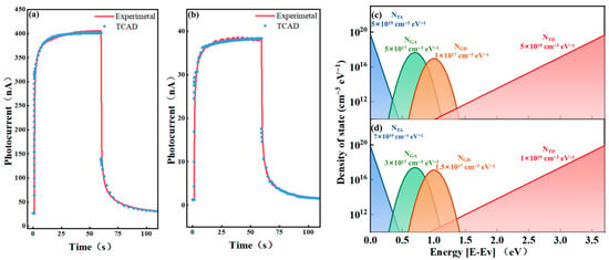
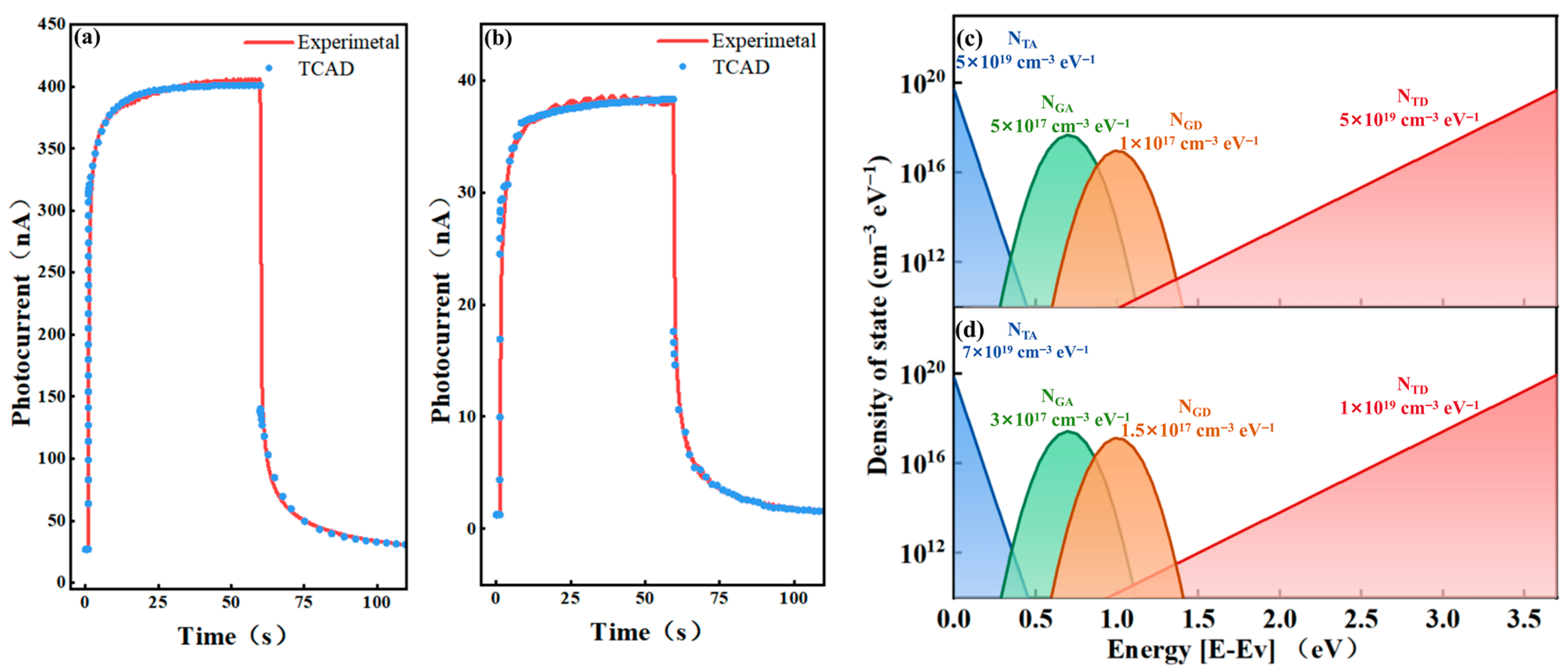
To further clarify the origin of responsivity differences among samples prepared under different conditions, two representative TFT-PDs (S4 and S7) are selected based on experimental results and modeled using TCAD. TCAD simulations offer detailed insights into device-level behaviors that are not accessible from VTH analysis alone, such as carrier dynamics and the spatial distribution of photon absorption. S4 is fabricated at 90 W with an Ar/O2 flow ratio of 40/0.3 sccm and a film thickness of 30 nm, whereas S7 is fabricated at 100 W with the same Ar/O2 flow ratio (40/0.3 sccm) and a thickness of 40 nm. In particular, the interfacial fixed charge Qf and the sub-gap DOS parameters (NTA/NTD and NGA/NGD) are extracted by fitting the measured transient I–t responses, providing a quantitative link to the process-dependent trends discussed in Section 3.2. The two devices are simulated under identical device geometry, bias conditions, and illumination settings. Figure 3a,b compare the experimental and simulated I-t curves of S4 and S7 under illumination. The TCAD simulations reproduced almost the same transient responsivity curves observed in the experiments, including the same responsivity amplitude and transient dynamics. Based on simulation results, we compared the extracted model parameters to identify device-level origins of the performance differences. Figure 3c,d present the extracted sub-gap defect-state density of states (DOS) for S4 and S7; the fitted parameters are summarized in Table 3. Pronounced differences are observed in interface fixed charge density and the densities of tail states and deep-level defect states. The S7 shows higher interface fixed charge and defect-state densities than the S4. The higher sputtering power (100 W) of S7 may increase the kinetic energy of sputtered species and aggravate interface damage and local disorder during growth, leading to higher interface fixed charge and defect densities. In addition, the thicker a-GaOx layer in S7 (40 nm) may weaken gate control and increase bulk trapping compared with S4 (30 nm), which can further degrade the transient responsivity and the extracted defect-related parameters. In contrast, S4 is fabricated under less aggressive conditions (90 W and 30 nm) and shows lower extracted interface and defect-related parameters, consistent with its stronger responsivity.
Figure 3.
TCAD fitting and defect-parameter extraction for representative devices with distinct responsivity. The I-t curves are measured and simulated under 254 nm illumination with a power density of 0.741 µW∙cm−2 at VDS = 10.1 V; the bias settings are consistent with the experiment, and VGS is fixed at VON defined from the dark transfer curve. (a) Experimental and TCAD-simulated I-t curves of S4 under 254 nm UV illumination; (b) experimental and TCAD-simulated I-t curves of S7 under 254 nm UV illumination; (c) extracted defect-state density of states (DOS) for S4 used in the TCAD fitting; (d) extracted defect-state DOS for S7 used in the TCAD fitting.
Table 3.
Key parameters extracted from TCAD fitting of the I-t curves for S4 and S7.
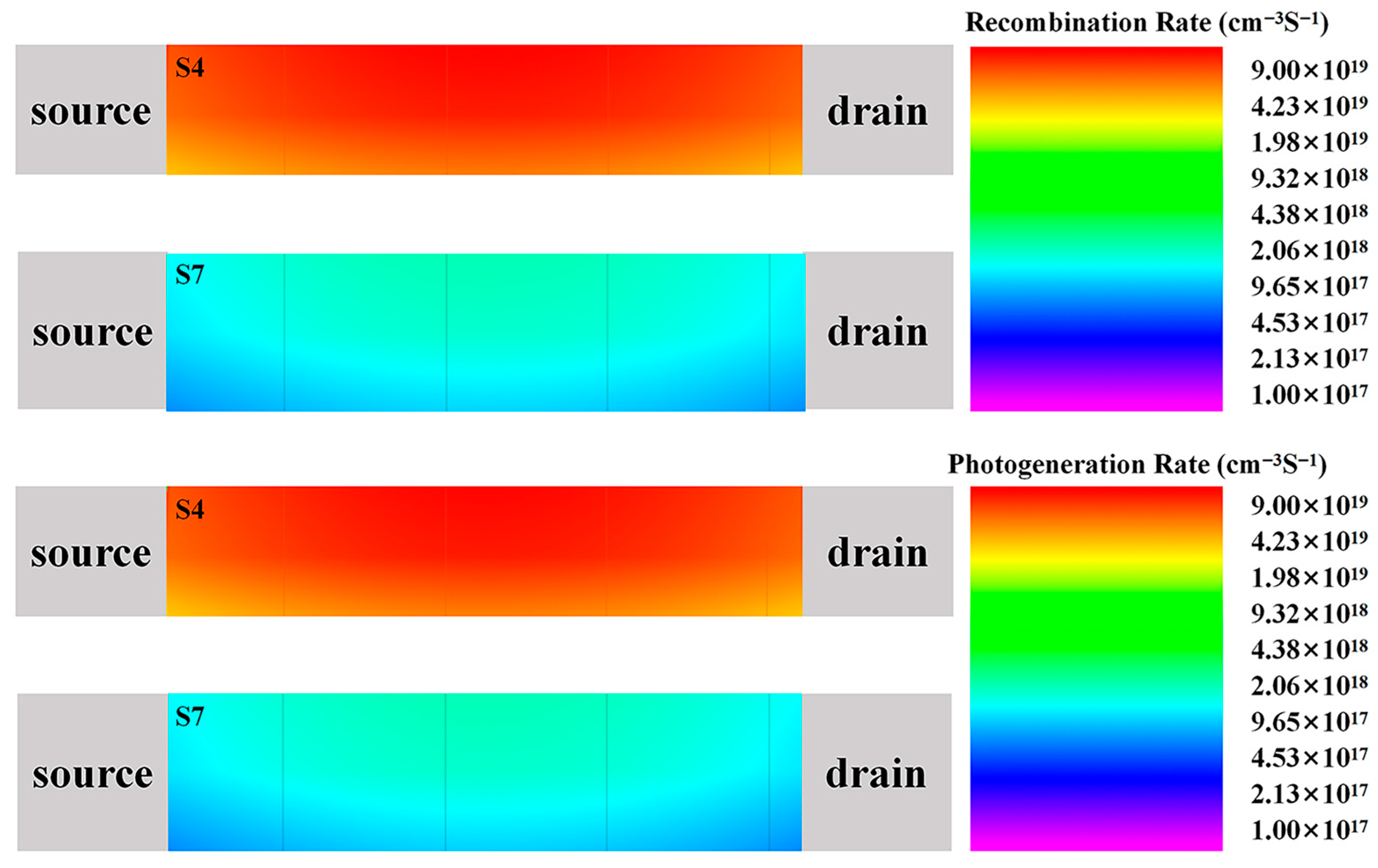
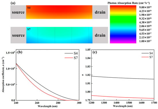
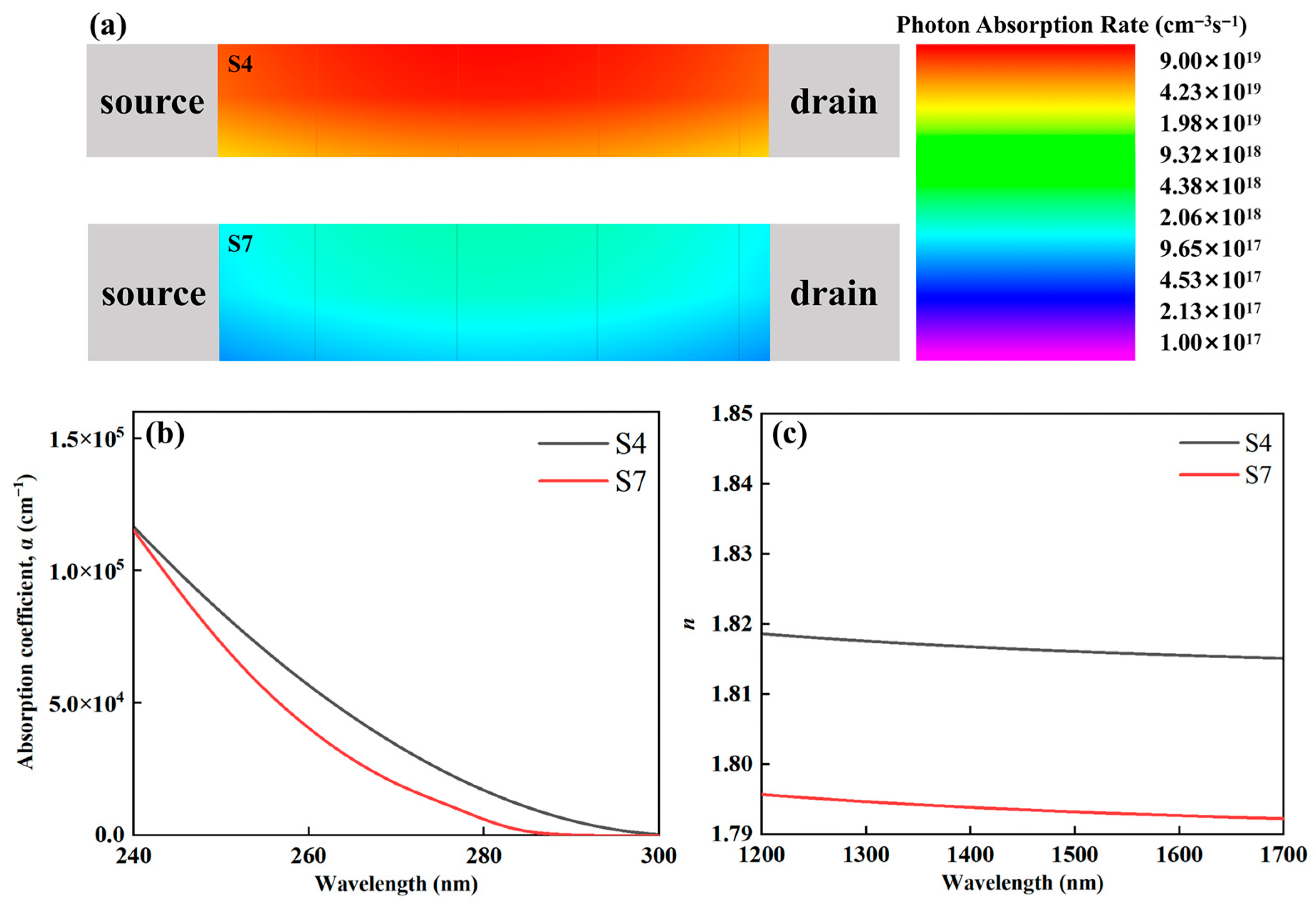
Figure 4a shows the spatial distribution of photon absorption rate in the channels of S4 and S7 under steady-state illumination. The overall absorption rate is higher in S4 than in S7 under the same illumination, which is consistent with the stronger absorption and higher carrier generation of S4, thus yielding experimentally higher photocurrent. In addition, the steady-state spatial distributions of the carrier generation and recombination rates from TCAD are shown in Figure A2. Both profiles follow the spatial distribution of the absorption in the channel. It demonstrates the higher generation rate of S4, which is consistent with its higher photocurrent.
Figure 4.
Simulated photon absorption and ellipsometry-derived optical properties of S4 and S7. (a) Simulated spatial distribution of photon absorption rate in the channel under steady-state illumination; (b) absorption coefficient (α) spectra of the S4 and S7 films in the 240–300 nm range measured by spectroscopic ellipsometry; (c) refractive index (n) spectra of the S4 and S7 films in the 1200–1700 nm range measured by spectroscopic ellipsometry.
To confirm the absorption difference, we performed spectroscopic ellipsometry on the S4 and S7 films. Figure 4b,c show the extracted absorption coefficients and refractive indices over the measured wavelength range. At a wavelength of 254 nm, the absorption coefficients of S4 and S7 are 71,879 and 57,410 cm−1, respectively, thus S4 absorbs more strongly at this wavelength. In general, thinner sputtered oxide films tend to be more affected by surface and interface states and may show higher effective defect density or porosity, which would not favor stronger band-to-band absorption and higher n values. The fact that S4 is thinner yet exhibits higher absorption and n values therefore supports that the observed difference is not a trivial thickness-related artifact but reflects a meaningful change in film quality controlled by the deposition conditions. Herein, it might be mainly attributed to variations in sputtering power. Moderate power can improve film densification, while higher power can increase bombardment and disorder during growth, which may deteriorate the film’s microstructure and optical constants.
4. Conclusions
This work mainly investigates the sputtering parameters on the optoelectronic performance of bottom-gate a-GaOx TFT-PDs using a three-factor, three-level orthogonal design. We evaluate the coupled roles of sputtering power, Ar/O2 flow ratio, and film thickness on the device performance based on the transfer curves and 254 nm I-t responses. Different parameter combinations lead to dramatic variations in transfer behavior and transient response, which affect photocurrent, photo/dark current ratio, and responsivity. Interface fixed charge density and trap-state parameters (tail and deep levels) are extracted based on TCAD simulation under the same experimental conditions, and these parameters are found to be highly dependent on the deposition conditions. The simulated photon absorption-rate profile closely matches the ellipsometry-derived absorption coefficients at 254 nm, confirming the presence of absorption differences. Together, the extracted trap parameters and absorption profile not only explain the responsivity differences across devices but also provide direct support for process optimization. This combined experimental–TCAD workflow is not limited to a-GaOx TFT photodetectors. It can be easily extended to other oxide-based TFT-PD systems, such as IGZO, ZnO, In2O3, or SnO2-based channels, where device performance is governed by similar factors, including process-dependent defect states, interfacial charge, and optical absorption. By combining orthogonal process screening with transient-response fitting and internal-physics analysis in TCAD, this approach offers a general framework to extract comparable defect/charge parameters and identify performance-limiting factors for optimization across a wide range of oxide-based photodetectors.
Author Contributions
Conceptualization, Y.C. and L.L.; methodology, M.L.; software, Y.C.; validation, J.R., C.X. and Y.X. (Yufang Xie); formal analysis, H.T.; investigation, H.W.; resources, H.C.; data curation, Y.X. (Yuting Xiong); writing—original draft preparation, Y.C.; writing—review and editing, L.L.; visualization, Y.C.; supervision, L.L.; project administration, L.L.; funding acquisition, H.C. All authors have read and agreed to the published version of the manuscript.
Funding
This research was funded by the Natural Science Foundation of China (62274166, 12304143).
Institutional Review Board Statement
Not applicable.
Informed Consent Statement
Not applicable.
Data Availability Statement
Data are contained within the article.
Acknowledgments
The authors acknowledge the help of Meng Xu in Shanghai University, for the construction of device models in TCAD simulations.
Conflicts of Interest
The authors declare no conflicts of interest.
Appendix A
Figure A1.
Variable-angle spectroscopic ellipsometry (VASE) data and model fitting results for a-GaOx films deposited on Si substrates. (a) S4 film; (b) S7 film.
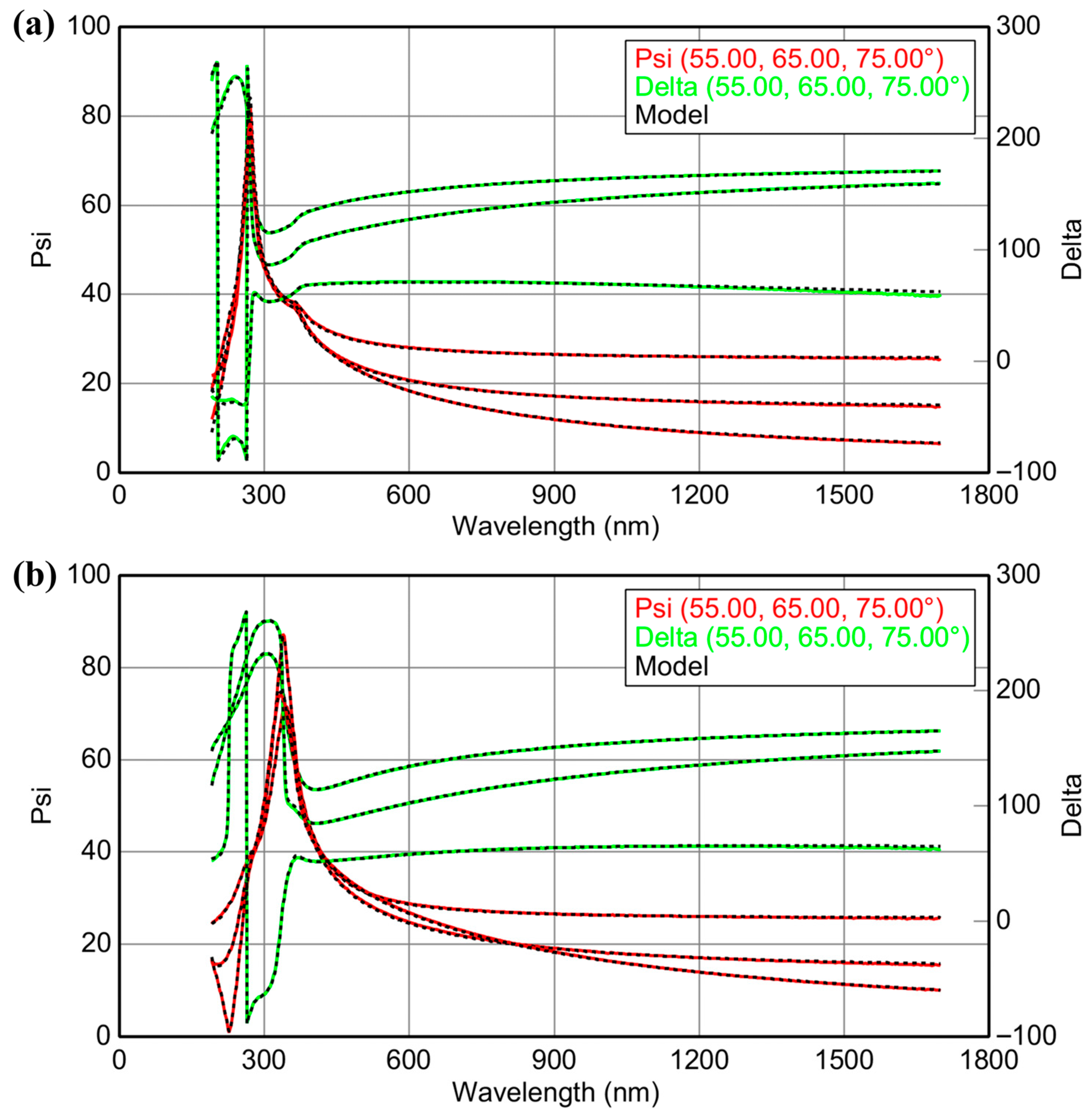
Figure A2.
TCAD-simulated steady-state spatial distributions of photogeneration and recombination rates in the channels of S4 and S7.
References
- Zhang, Y.; Liu, X.; Bi, Z.; Xu, R.; Chen, Y.; Zhou, J.; Ruan, S. An Ultraviolet Photodetector Based on In2O3/β-Ga2O3 Heterojunction. Mater. Sci. Semicond. Process. 2024, 181, 108648. [Google Scholar] [CrossRef] [Scilit]
- Zhang, Y.; Qin, Z.; Gao, H.; Wang, T.; Gao, C.; Zhang, X.; Hu, W.; Dong, H. Highly-Polarized Solar-Blind Ultraviolet Organic Photodetectors. Adv. Mater. 2024, 36, 2404309. [Google Scholar] [CrossRef] [Scilit]
- Zhang, R.; Wang, G.; Zhang, Q.; Wang, S.; Hu, X.; Liu, L.; Lv, S.; Chen, W.; Xu, X.; Zhang, L. Recent Progress in GaN-Based Ultraviolet Photodetectors. J. Mater. Chem. C 2025, 13, 10972–10996. [Google Scholar] [CrossRef] [Scilit]
- Zhang, N.; Wang, Z.; Lin, Z.; Zhu, S.; Cai, W.; Zhang, L.; Zhang, X.; Rong, M.; Zhang, X.; Chen, D.; et al. β-Ga2O3 Extreme Ultraviolet Photodetectors. Eur. Phys. J. Spec. Top. 2025, 234, 303–309. [Google Scholar] [CrossRef] [Scilit]
- Ko, R.-M.; Wang, S.-J.; Chen, Y.-H.; Liao, C.-Y.; Wu, C.-H. Using Thin-Film Transistor with Thick Oxygen-Doped Si-Zn-Sn-O Channel and Patterned Pt/NiO Capping Layer to Enhance Ultraviolet Light Sensing Performance. Jpn. J. Appl. Phys. 2024, 63, 02SP29. [Google Scholar] [CrossRef] [Scilit]
- Hwang, J.-D.; Liu, W.-Y. Hybrid Visible-Blind Ultraviolet Photodetector Based on NiO Thin-Film Phototransistor and p-NiO/n-Si Heterojunction Diode. Mater. Sci. Semicond. Process. 2022, 149, 106858. [Google Scholar] [CrossRef] [Scilit]
- Wang, Y.; Xue, Y.; Su, J.; Lin, Z.; Zhang, J.; Chang, J.; Hao, Y. Realization of Cost-Effective and High-Performance Solar-Blind Ultraviolet Photodetectors Based on Amorphous Ga2O3 Prepared at Room Temperature. Mater. Today Adv. 2022, 16, 100324. [Google Scholar] [CrossRef] [Scilit]
- Qin, Y.; Li, L.H.; Yu, Z.; Wu, F.; Dong, D.; Guo, W.; Zhang, Z.; Yuan, J.H.; Xue, K.H.; Miao, X.; et al. Ultra-High Performance Amorphous Ga2O3 Photodetector Arrays for Solar-Blind Imaging. Adv. Sci. 2021, 8, 2101106. [Google Scholar] [CrossRef] [Scilit]
- Peng, K.; Xue, D.; Li, N.; Lin, W.; Chen, C.; Lv, P. Depletion-Mode A-GaOx Solar-Blind Phototransistors for Optoelectronic Mixed Logic Gate Circuit and Solar-Blind Imaging. ACS Appl. Mater. Interfaces 2025, 17, 43199–43207. [Google Scholar] [CrossRef] [Scilit]
- Liu, H.; Zhou, S.; Zhang, H.; Ye, L.; Xiong, Y.; Yu, P.; Li, W.; Yang, X.; Li, H.; Kong, C. Ultrasensitive Fully Transparent Amorphous Ga2O3 Solar-Blind Deep-Ultraviolet Photodetector for Corona Discharge Detection. J. Phys. D Appl. Phys. 2022, 55, 305104. [Google Scholar] [CrossRef] [Scilit]
- Cui, S.; Mei, Z.; Zhang, Y.; Liang, H.; Du, X. Room-Temperature Fabricated Amorphous Ga2O3 High-Response-Speed Solar-Blind Photodetector on Rigid and Flexible Substrates. Adv. Opt. Mater. 2017, 5, 1700454. [Google Scholar] [CrossRef] [Scilit]
- Zhu, W.; Xiong, L.; Si, J.; Hu, Z.; Gao, X.; Long, L.; Li, T.; Wan, R.; Zhang, L.; Wang, L. Influence of Deposition Temperature on Amorphous Ga2O3 Solar-Blind Ultraviolet Photodetector. Semicond. Sci. Technol. 2020, 35, 055037. [Google Scholar] [CrossRef] [Scilit]
- Zhou, C.; Liu, K.; Chen, X.; Feng, J.; Yang, J.; Zhang, Z.; Liu, L.; Xia, Y.; Shen, D. Performance Improvement of Amorphous Ga2O3 Ultraviolet Photodetector by Annealing under Oxygen Atmosphere. J. Alloys Compd. 2020, 840, 155585. [Google Scholar] [CrossRef] [Scilit]
- Zhang, T.; Guan, D.; Liu, N.; Zhang, J.; Zhang, J.; Guo, C.; Qiu, M.; Yuan, Q.; Zhang, W.; Ye, J. Room Temperature Fabrication and Post-Annealing Treatment of Amorphous Ga2O3 Photodetectors for Deep-Ultraviolet Light Detection. Appl. Phys. Express 2022, 15, 022007. [Google Scholar] [CrossRef] [Scilit]
- Zhou, H.; Cong, L.; Ma, J.; Chen, M.; Song, D.; Wang, H.; Li, P.; Li, B.; Xu, H.; Liu, Y. High-Performance High-Temperature Solar-Blind Photodetector Based on Polycrystalline Ga2O3 Film. J. Alloys Compd. 2020, 847, 156536. [Google Scholar] [CrossRef] [Scilit]
- Gu, K.; Zhang, Z.; Tang, K.; Huang, J.; Liao, M.; Wang, L. Effects of Sputtering Pressure and Oxygen Partial Pressure on Amorphous Ga2O3 Film-Based Solar-Blind Ultraviolet Photodetectors. Appl. Surf. Sci. 2022, 605, 154606. [Google Scholar] [CrossRef] [Scilit]
- Hun Yu, J.; Lee, W.-J.; Cho, D.-H.; Kim, W.-J.; Jun Kang, S.; Chung, Y.-D. The Origin of the Enhanced Photoresponsivity of the Phototransistor with ZnO1−xSx Single Active Layer. Appl. Surf. Sci. 2022, 590, 153062. [Google Scholar] [CrossRef] [Scilit]
- Yoon, Y.; Kim, Y.; Shin, M. Impact of Channel Thickness and Doping Concentration for Normally-Off Operation in Sn-Doped β-Ga2O3 Phototransistors. Sensors 2024, 24, 5822. [Google Scholar] [CrossRef] [Scilit]
- Jang, Y.; Lee, S.-Y. In Situ IGZO/ZnON Phototransistor Free of Persistent Photoconductivity with Enlarged Spectral Responses. ACS Appl. Electron. Mater. 2023, 5, 509–519. [Google Scholar] [CrossRef] [Scilit]
- Vidal Lorbada, R.; Walter, T.; Fuertes Marrón, D.; Muecke, D.; Lavrenko, T.; Salomon, O.; Schaeffler, R. Phototransistor Behavior in CIGS Solar Cells and the Effect of the Back Contact Barrier. Energies 2020, 13, 4753. [Google Scholar] [CrossRef] [Scilit]
- Hu, C.; Li, P.; Wang, L.; Li, S.; Lv, B.; Wang, Y.; Ma, J. Theoretical Study on the Role of Gating and Photoconduction on Ga2O3 Phototransistors. IEEE Sens. J. 2023, 23, 26894–26899. [Google Scholar] [CrossRef] [Scilit]
- Park, J.B.; Kim, J.; Jang, Y.W.; Park, H.B.; Yang, S.H.; Kim, D.H.; Kim, M.; Facchetti, A.; Park, S.K. Analysis of Carrier Transport in Quantum Dot/Metal-Oxide Phototransistors via Light-Mediated Interfacial Modeling. Adv. Opt. Mater. 2023, 11, 2201559. [Google Scholar] [CrossRef] [Scilit]
- Kim, M.S.; Lee, G.J.; Kim, H.M.; Song, Y.M. Parametric Optimization of Lateral NIPIN Phototransistors for Flexible Image Sensors. Sensors 2017, 17, 1774. [Google Scholar] [CrossRef] [Scilit]
- Bashir, I.; Amin, S.I.; Majeed, L.; Rasool, Z.; Anand, S. Comprehensive Analysis of Single and Double Gate Organic Phototransistor. Opt. Quantum Electron. 2023, 55, 1095. [Google Scholar] [CrossRef] [Scilit]
- Gao, L.; Zhang, N.; You, J.; Wang, B.; Zhang, B.; Han, Z.; Jiang, Z.; Miao, T.; Guo, H.; Zhang, J.; et al. Broadband and Ultra-High-Sensitivity Separate Absorption-Multiplication Avalanche Phototransistor Based on a Au-WSe2-Ge Heterostructure. ACS Photonics 2023, 10, 4349–4356. [Google Scholar] [CrossRef] [Scilit]
- Su, W.; Wang, H.; Zou, Z.; Chai, C.; Weng, S.; Ye, J.; Sun, J.; Yan, Q.; Zhou, X.; Wu, C.; et al. Design and Photomodulation Performance of a UV-Driven Full GaN Integrated μLED and BJT Phototransistor. ACS Photonics 2024, 11, 649–659. [Google Scholar] [CrossRef] [Scilit]
- Lin, L.; Jiang, L.; Li, P.; Xiong, H.; Lien, S.Y.; Chen, D.; Lin, X.; Jiang, H.; Fan, B.; Qiu, Y. Design and Performance Optimization of a Novel Perovskite Photodetector Based on a Bipolar Heterojunction Phototransistor. J. Comput. Electron. 2025, 24, 65. [Google Scholar] [CrossRef] [Scilit]
- Kim, J.; Yoon, Y.; Shin, M.; Hwang, J. Near-Infrared Phototransistor Using a SiGe-Based Light-Triggered Feedback Field-Effect Transistor with a Metasurface. ACS Photonics 2025, 12, 809–818. [Google Scholar] [CrossRef] [Scilit]
- Khurana, M.; Saxena, M.; Gupta, M. Highly Sensitive Ga2O3-Face Tunnel Field Effect Phototransistor for Deep UV Detection. IEEE Sens. J. 2022, 22, 17769–17776. [Google Scholar] [CrossRef] [Scilit]
- Huzaibi, H.U.; Han, S.T.; Zhang, M. Model representation in amorphous metal oxide thin-film transistors: A critical review. npj Flex. Electron. 2026, 10, 13. [Google Scholar] [CrossRef] [Scilit]
- Huang, X.; Chen, C.; Sun, F.; Chen, X.; Xu, W.; Li, L. Enhancing the Carrier Mobility and Bias Stability in Metal–Oxide Thin Film Transistors with Bilayer InSnO/a-InGaZnO Heterojunction Structure. Micromachines 2024, 15, 512. [Google Scholar] [CrossRef] [Scilit] [PubMed]
- Hsieh, H.-H.; Kamiya, T.; Nomura, K.; Hosono, H.; Wu, C.-C. Modeling of amorphous InGaZnO4 thin film transistors and their subgap density of states. Appl. Phys. Lett. 2008, 92, 133503. [Google Scholar] [CrossRef] [Scilit]

Disclaimer/Publisher’s Note: The statements, opinions and data contained in all publications are solely those of the individual author(s) and contributor(s) and not of MDPI and/or the editor(s). MDPI and/or the editor(s) disclaim responsibility for any injury to people or property resulting from any ideas, methods, instructions or products referred to in the content. |
© 2026 by the authors. Licensee MDPI, Basel, Switzerland. This article is an open access article distributed under the terms and conditions of the Creative Commons Attribution (CC BY) license.