Article

Effects of Si Target Power on the Mechanical Properties and Antioxidation and Antiablation Properties of Magnetron-Sputtered (WMoTaNb)SiN Refractory High-Entropy Nitride Films

School of Materials Science and Chemical Engineering, Xi’an Technological University, Xi’an 710021, China
*
Authors to whom correspondence should be addressed.
Coatings 2026, 16(3), 309; https://doi.org/10.3390/coatings16030309
Submission received: 27 January 2026 / Revised: 21 February 2026 / Accepted: 27 February 2026 / Published: 2 March 2026

Abstract

(WMoTaNb)SiN refractory high-entropy nitride films were deposited via magnetron cosputtering, and the Si content was systematically regulated by varying the Si target power to investigate its influence on the microstructure, mechanical properties, oxidation resistance, and oxyhydrogen-flame ablation behavior. All the films exhibited dense columnar architectures with a distinct FCC + BCC dual-phase structure, whereas increasing the Si target power led to a gradual increase in the deposition rate and Si incorporation. The mechanical properties displayed a non-monotonic relationship with the Si target power, with film applied at an intermediate level of Si target power showing the highest hardness, approximately 28.5 GPa, and improved elastic recovery. Tribological evaluations using a GCr15 steel ball revealed that this film exhibited the lowest wear rate of 4.1 × 10⁻⁶ mm3·N−1·m−1 and a narrower wear track, which was attributed to reduced plastic deformation and the development of an oxygen-enriched tribofilm during sliding. High-temperature oxidation at 1000 °C in air revealed that Si incorporation significantly modified oxide-scale evolution by refining the oxidation products and altering the scale architecture, while the protection of the scale was governed by its continuity and compactness rather than its thickness alone. Oxyhydrogen-flame ablation tests revealed that the degradation behavior was primarily driven by the competition between oxidation-induced mass increase and ablation-induced material loss, with localized film disruption and substrate exposure playing a decisive role. In summary, the findings illustrate that an optimal Si target power establishes a favorable equilibrium between mechanical strength, tribological efficiency, oxidation resistance, and ablation performance, underscoring the potential of (WMoTaNb)SiN films for protective applications in complex mechanical and extreme thermal environments.

1. Introduction

Refractory high-entropy nitride (RHEN) films have attracted sustained attention for thermal protection and high-temperature structural applications because they can concurrently deliver high hardness, thermal stability, and chemical inertness [1,2,3,4,5,6,7,8]. In real-world applications, however, film failure is seldom influenced by a single factor. Instead, oxidation-driven degradation, thermally induced cracking, spallation, and oxidation-facilitated material loss can act synergistically under intense thermal fluxes, ultimately compromising surface integrity and reducing component lifetime. As a result, developing nitride films that maintain mechanical strength, prevent oxygen infiltration, and resist ablation continues to present a significant challenge.
High-entropy nitrides, derived from multiprincipal-element refractory systems, provide a viable pathway to overcome the limitations of conventional binary or ternary nitrides. Prior studies have shown that many RHEN films tend to form predominantly FCC-type solid-solution structures, which are occasionally accompanied by minor secondary features depending on the deposition conditions, and they often exhibit high hardness together with promising wear resistance [9,10,11]. The observed strengthening has been ascribed to a combination of factors, including significant lattice distortion, solid-solution strengthening, and microstructural refinement, while the growth morphology and defect density can be further adjusted through bias voltage, nitrogen partial pressure, and target power [12]. Despite these advantages, the oxidation behavior of refractory high-entropy nitride films is frequently complicated by the concurrent formation of multiple metal oxides and complex oxides, which may grow rapidly and exhibit porous or nonprotective morphologies. Repeated cracking and spallation of such scales under thermal cycling can further accelerate mass transport and exacerbate material loss [13,14,15,16,17].
The incorporation of Si into nitride films has been extensively explored as an effective microstructural design strategy. Previous studies have demonstrated that Si incorporation is an effective strategy for tailoring the microstructure and performance of hard coatings. In Si-containing nitride systems, introducing Si and adjusting deposition parameters can significantly influence phase constitution, grain growth behavior, and the development of amorphous intergranular components, thereby affecting hardness, adhesion, and tribological performance. Similar power-dependent effects have also been reported in Si-containing carbon-based coatings, where sputtering power modifies the film microstructure and frictional response. In addition, studies on TiAlSiN-based coatings further indicate that the coupling among hardness, adhesion, and wear behavior is highly sensitive to Si-related compositional and structural regulation. These findings collectively confirm the effectiveness of Si-assisted microstructural engineering while also suggesting that the underlying structure–property relationships remain system-dependent and require further clarification in refractory high-entropy nitride films, especially under coupled wear, oxidation, and ablation conditions [18,19,20,21,22,23]. In a broad range of transition-metal nitride systems, Si addition has been reported to promote nanostructuring and densification, sometimes leading to nanocomposite architectures consisting of nanocrystalline MeN embedded in an amorphous SiNx matrix, which can increase hardness and improve resistance to plastic deformation [24]. In parallel, Si incorporation is widely recognized to be beneficial for oxidation resistance because Si-containing nitrides may generate SiO2-rich products during high-temperature exposure. These silica-derived phases can seal diffusion pathways, improve scale continuity, and act as effective barriers against inward oxygen transport, thereby suppressing the development of porous oxides. However, the effectiveness of Si is not universal and is highly dependent on factors such as Si content, phase constitution, and the competition between protective scale formation, especially under extreme thermal conditions, where melt flow, volatilization, and substrate exposure may take place [12].
To address these issues, the present work investigates the influence of Si target power on the structure–property–performance relationships of magnetron-sputtered (WMoTaNb)SiN films. A series of films with progressively increased Si contents was produced by dual-target cosputtering, enabling a systematic evaluation of the phase constitution, microstructural characteristics, and mechanical response, together with the tribological behavior. Furthermore, the oxidation and ablation resistance of these films were investigated by conducting high-temperature oxidation in air at 1000 °C and using oxygen-hydrogen flame ablation. Microscopic structure and composition analyses were also performed on representative areas to elucidate the degradation and protection mechanisms. By correlating the Si target power with microstructure evolution and performance metrics relevant to service, this study seeks to identify an optimized Si incorporation range and offer guidance for designing RHEN films with enhanced oxidation and ablation tolerance.

2. Experiment

2.1. Film Preparation

(WMoTaNb)SiN films were deposited on Si (100) wafer and M2 steel plates via an RF + DC dual-target magnetron sputtering system (VTC-600-2HD, Shenyang Kejing Ltd., Shenyang, China). The Si substrates were mainly used for phase-structure characterization (for example, XRD (Shanghai Erdi Instrument Technology Co., Ltd., Shanghai, China), whereas the M2 steel substrates were used for mechanical, tribological, oxidation, and ablation tests. It should be noted that substrate type may influence the initial growth behavior, residual stress state, and microstructural evolution of the films. In the present work, however, comparative analyses for each property were conducted on the same substrate type, so the relative effect of Si target power remains meaningful within each test series. The Si target is connected to the DC (Direct Current) target, and the high-entropy alloy target WMoTaNb is connected to the RF (Radio Frequency) target. The Si target (99.9%) and the WMoTaNb (1:1:1:1 at.%, 99.9%) target were produced by Beijing YanBang New Material Science and Technology Co., Ltd. (Beijing, China), and the targets had a diameter of 50.4 mm and a thickness of 3 mm. The substrates were ultrasonically cleaned in acetone and anhydrous ethanol for 10 min each prior to deposition to remove surface oils and contaminants. The target material subsequently underwent 20 min of presputtering to eliminate surface oxides. The deposition parameters are detailed in Table 1.

2.2. Film Characterization

The compositions of the (WMoTaNb)SiN RHEAN films were determined via EDS (Energy-dispersive X-ray spectroscopy, Oxford Instruments Technology (Shanghai) Co., Ltd., Shanghai, China). It should be noted that the quantification of Si in the W-containing films by EDS may be affected by the spectral overlap between Si Kα and W Mα lines. Therefore, the EDS results involving Si are used in this work mainly for comparative trend analysis among samples prepared under identical conditions, rather than as absolute quantitative values. The crystal structure of the films was examined via X-ray diffraction (XRD, D8 Phaser, Bruker, Shanghai Erdi Instrument Technology Co., Ltd., Shanghai, China) with Cu-Kα radiation (wavelength of 0.15406 nm) at a scan speed of 2°/min (over a 2θ range from 20° to 100°). The surface and cross-sectional morphologies, together with the chemical compositions of the films, were investigated via field-emission SEM (Scanning Electron Microscopy, Fonar Scientific Instruments (Shanghai) Co., Ltd., Shanghai, China). The hardness (H) and elastic modulus (E) of the films were obtained via nanoindentation (G200, Agilent, Beijing Zhonghai Yuanchuang Materials Technology Co., Ltd., Beijing, China) via a Berkovich diamond indenter at room temperature, and the displacement of the indenter was limited to 100 nm. Scratch test measurements were conducted on the films with a scratch tester (WS-2005, Lanzhou Zhongke Kaihua Technology Development Co., Ltd., Lanzhou, China) to evaluate the adhesion quality. The critical load of the films was determined by recording the acoustic signals during the scratch test of the scratch track.
Dry sliding wear testing was performed via a ball-on-disc tribometer (HT-1000, Lanzhou Zhongke Kaihua Technology Development Co., Ltd., Lanzhou, China). The grinding ball consisted of a GCr15 ball (HV ~ 63 HRC) with a diameter of 6 mm. Test parameters such as load, speed, wear radius, and duration were set at 200 g, 5 m/min, 3 mm, and 20 min, respectively. After the wear tests, a Zygo NewView 8200 three-dimensional profilometer (Shanghai Wodun Precision Equipment Technology Co., Ltd., Shanghai, China) was used to measure the three-dimensional profiles of the wear tracks. In this work, the reported wear rate refers to the wear rate of the films and was determined from the wear-track volume loss of the film side (obtained from the wear-track geometry/profile). The wear of the GCr15 steel ball counterface was not included in the wear-rate calculation.
The high-temperature oxidation test was performed in a box-type resistance (Sigma (Shanghai) High Temperature Electric Furnace Co., Ltd., Shanghai, China) furnace under atmospheric pressure. The samples were heated from room temperature to 1000 °C at a rate of 10 °C per minute, oxidized at this high temperature for 2 h, then removed and cooled to room temperature via air cooling. Oxyacetylene ablation tests were performed to simulate the high-temperature ablation environment and evaluate the ablation resistance of the film. Each reaction lasted for 0.5 s, for a total of 8 times. After testing, the samples were cooled naturally to room temperature in air and subsequently weighed.

3. Results and Discussion

3.1. Microstructure

Figure 1 presents the XRD patterns of the (WMoTaNb)SiN films deposited on Si substrates. Phase indexing was conducted by matching the diffraction peaks against the ICDD PDF-4+ database. The films exhibit a distinct FCC (Face-centered cubic) +BCC (Body-centered cubic) dual-phase feature, while Si substrate reflections are detected because of the thin film thickness and the high penetrability of X-rays. It should be noted that the substrate can influence the initial film growth and microstructural evolution; therefore, the XRD results in Figure 1 are interpreted as phase-structure information for films grown on Si substrates under identical deposition conditions. It should be emphasized that the intense peak at approximately 62° as well as other reflections labeled as Si are contributed by the Si substrate rather than the films, and therefore they are indexed as substrate peaks. Nevertheless, with increasing Si target power, the intensity of the main film-related diffraction peaks first increases and then decreases, indicating that moderate Si target power favors crystallization, whereas excessive Si introduction suppresses crystalline growth. In addition, a diffuse broad hump is observed in the range of 20–30°, suggesting the increased amorphous contribution induced by Si incorporation, which indicates significant changes in the film crystal structure and microstructural state [24,25].
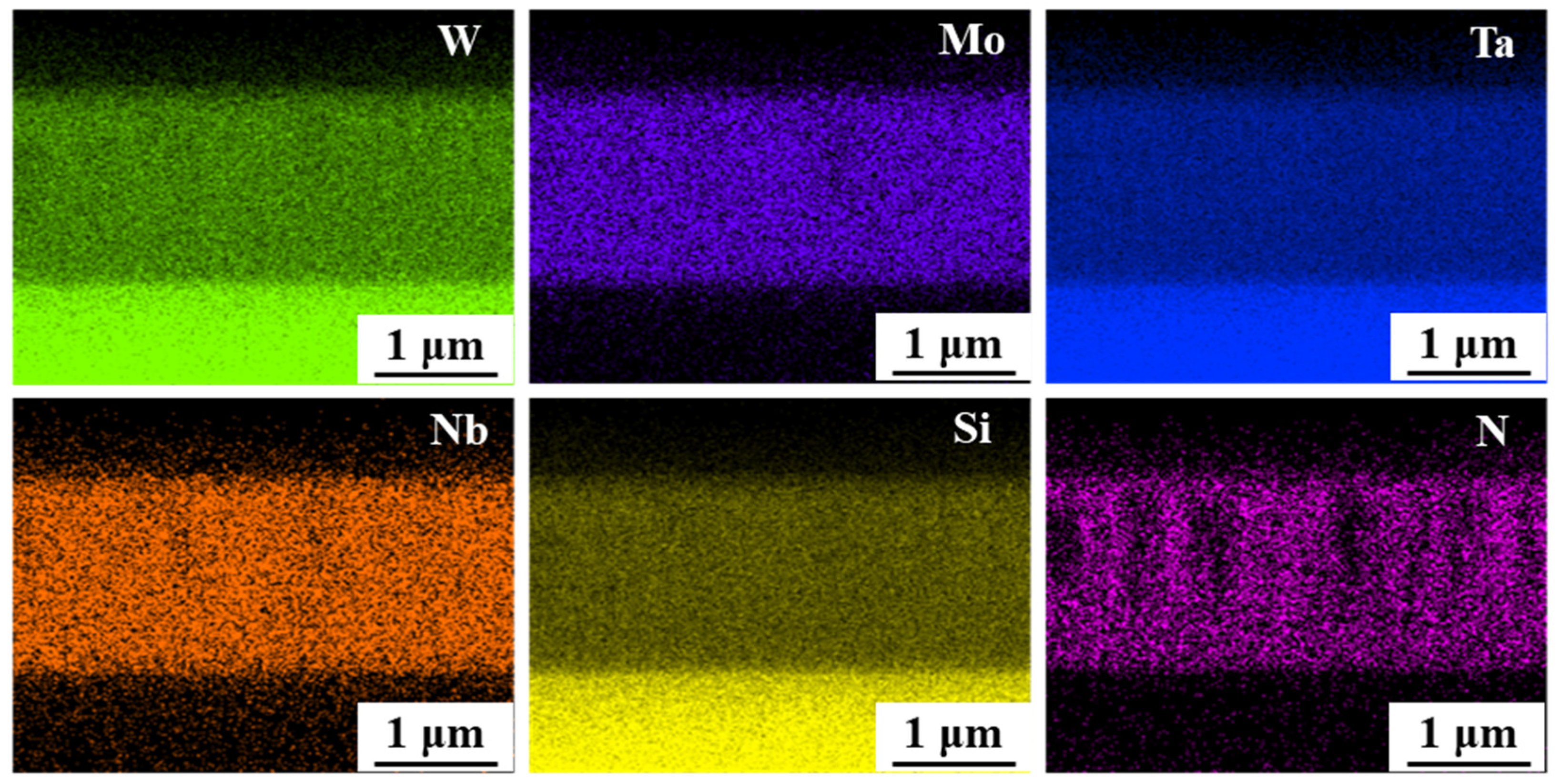
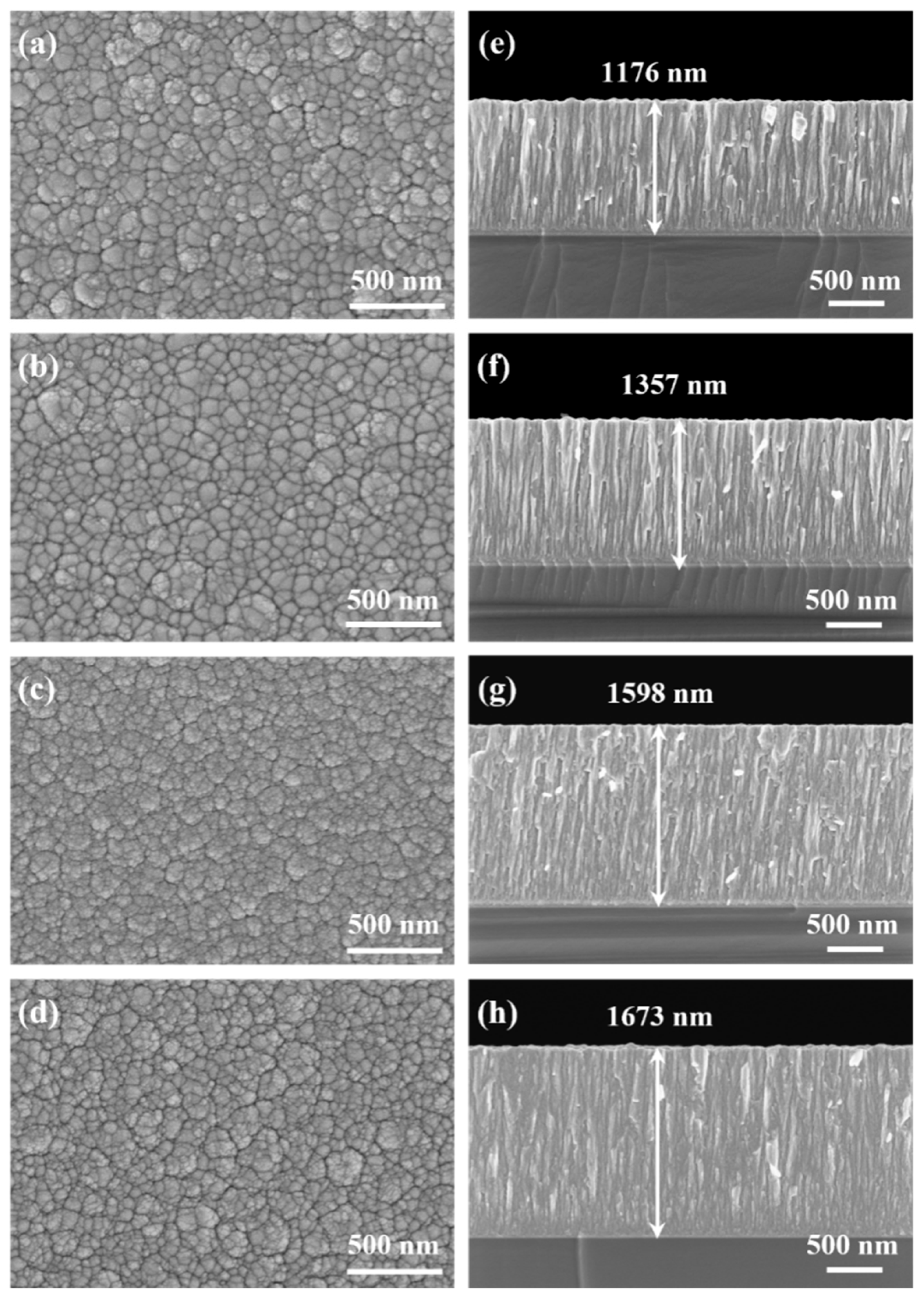
Figure 2 shows SEM images of the surface and cross-sectional morphology of the as-deposited (WMoTaNb)SiN film. A comparison of the surface morphologies revealed that the film surface presented cauliflower-like clusters. With increasing Si target power, the overall size of the surface cluster particles tends to decrease in general, indicating that the introduction of Si plays a role in grain refinement [9]. The cross-sectional morphologies of the films showed typical columnar growth structures in all samples. The effect of Si target power is mainly reflected in the variation of columnar compactness and microstructural features, rather than a structural transition from disorder to columnar growth. As the Si target power keeps increasing, the thickness of the film also shows a trend of increasing. This phenomenon indicates that the growth behavior of the films is significantly affected by the Si target power. Two main factors contribute to this phenomenon: First, differences in the crystal structure between the substrate and the film result in disordered structures during the initial film growth stage. However, the introduction of Si is considered to modify the initial growth behavior at the film-substrate interface by changing the deposition kinetics and subsequent microstructural evolution. It should be noted that residual stress was not quantified in the present work; therefore, the interfacial evolution is discussed here based on microstructural observations rather than direct stress analysis. Second, as the Si power increases, the energy carried by high-energy particles also increases, leading to an increase in the sputtering rate of the particles and subsequently an increase in the growth rate of the films. Figure 3 shows EDS elemental maps obtained from the area shown in Figure 2h. The results confirmed the formation of (WMoTaNb)SiN films, and the constituent elements were overall distributed in the film region, although local contrast variations (especially for N) can be observed in the EDS maps [17,26,27]. Such local contrast variations may be associated with microstructural contrast and the intrinsic limitations of cross-sectional EDS mapping and therefore should be interpreted with caution.
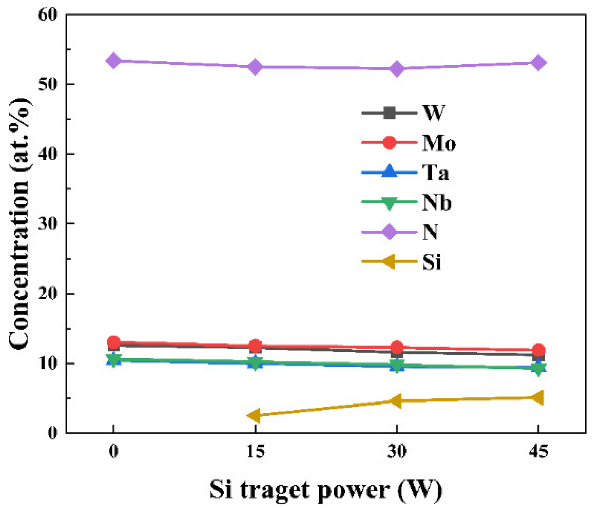
Figure 4 shows the elemental compositions of the as-deposited (WMoTaNb)SiN films. With increasing Si target power, the detected Si content in the films shows an increasing trend. However, it should be noted that the absolute Si values obtained by EDS may contain uncertainty due to the spectral overlap between Si Kα and W Mα lines. Therefore, the data in Figure 4 are interpreted here primarily in terms of the relative compositional evolution with Si target power, rather than strict absolute quantification of Si content. With increasing Si target power, the EDS-detected Si content exhibits an overall increasing trend, indicating that increasing Si target power promotes Si incorporation into the films under the present deposition conditions. At the same time, the increase in the detected Si content is relatively moderate. This should be interpreted with caution because the absolute quantification of Si by EDS in W-containing films may be affected by the spectral overlap between Si Kα and W Mα lines, which can introduce uncertainty into the measured Si values. Therefore, the compositional results in Figure 4 are used in this work primarily to reflect the relative compositional evolution with Si target power, and the observed trend remains consistent with the changes in XRD features and the corresponding mechanical, tribological, and oxidation behaviors.

3.2. Mechanical Properties

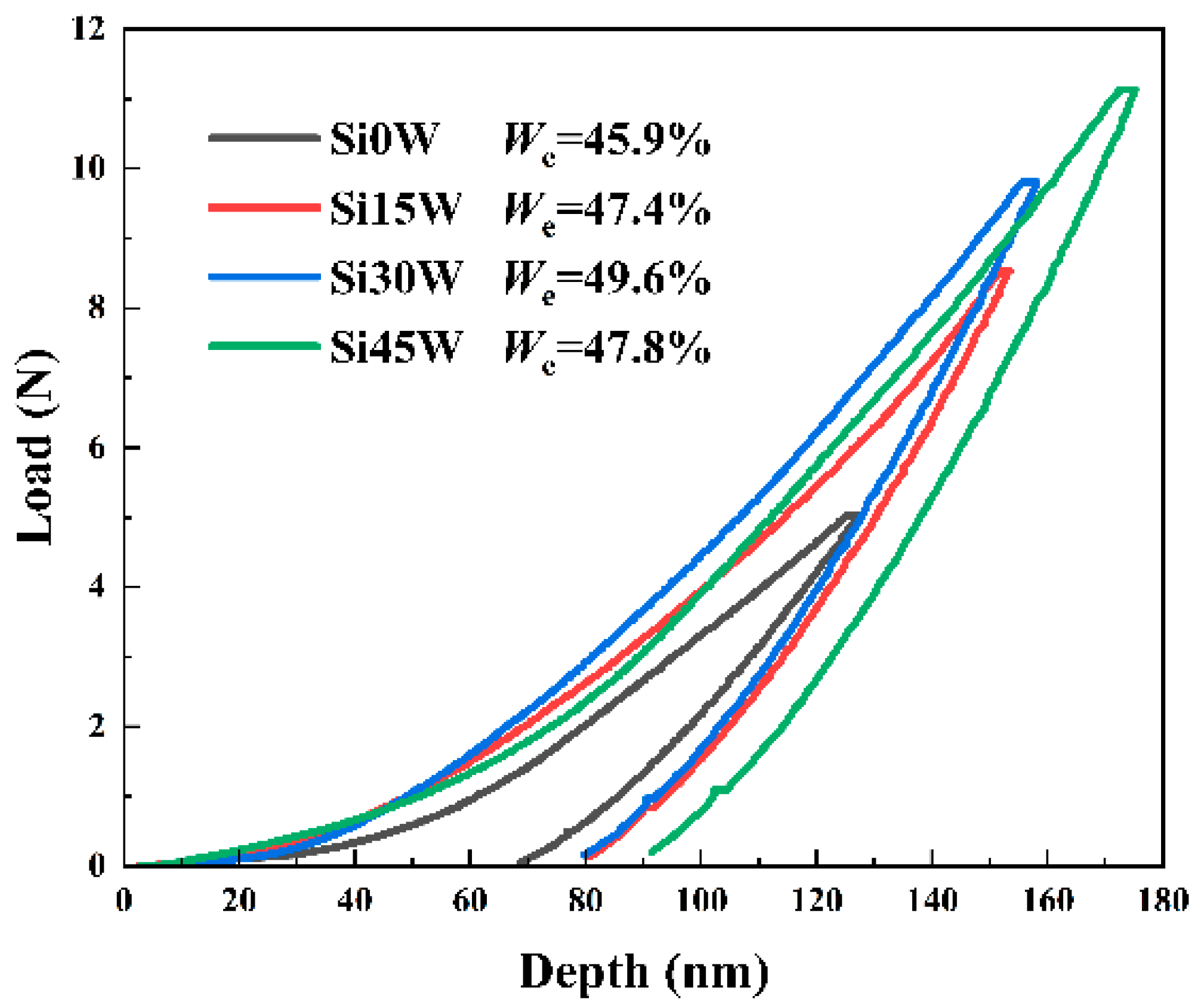
For the (WMoTaNb)SiN films deposited under different Si target powers, representative nanoindentation load-displacement curves are presented in Figure 5. Nanoindentation results indicate that the (WMoTaNb)SiN films exhibit an indentation depth of approximately 10% of the film thickness. With increasing Si target power, the slope of the indentation curve first tends to increase but then decreases, indicating that the deformation resistance of the (WMoTaNb)SiN films is enhanced. As a result, the elastic recovery rate initially increases and then decreases with increasing Si target power, reaching a maximum value of 49.6% when the Si target power is 30 W. This trend indicates a notable improvement in the plasticity of RHEAN films due to the introduction of Si [28].
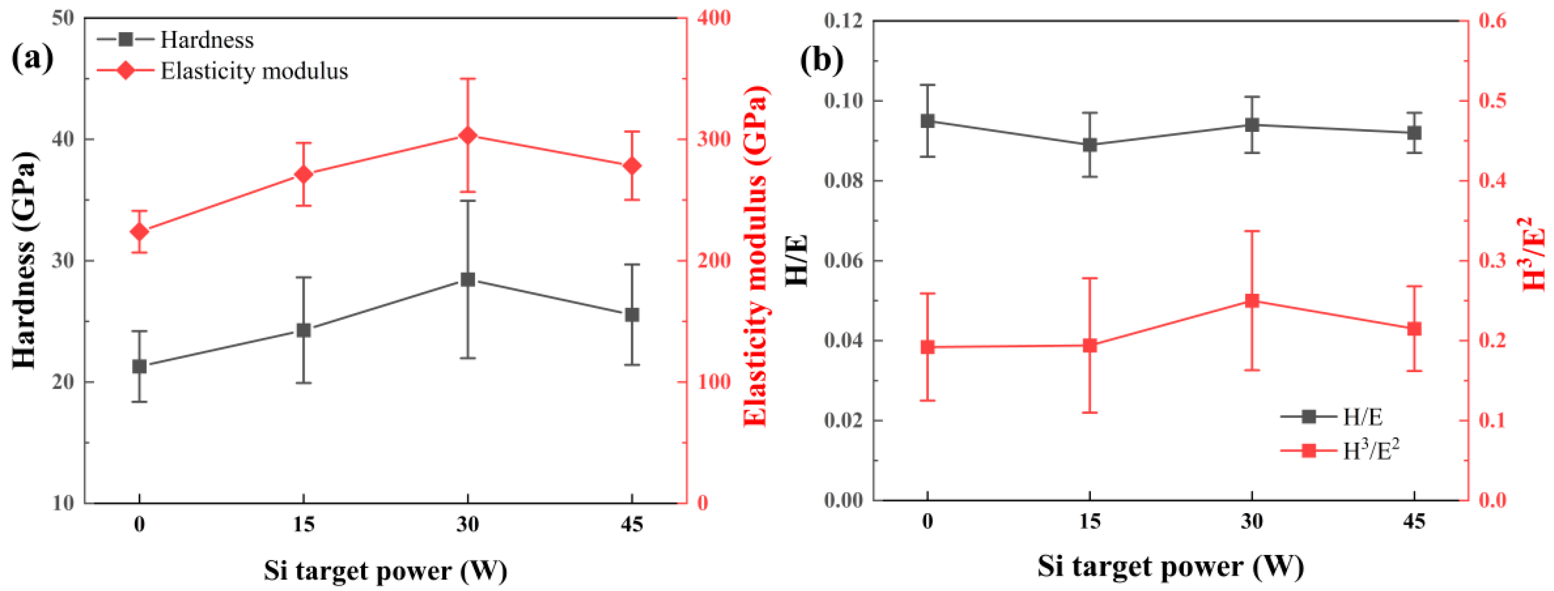
Figure 6a presents the curves of hardness (H) and elastic modulus (E) for (WMoTaNb)SiN films prepared under different Si target powers. The hardness and elastic modulus values of the (WMoTaNb)SiN film are 21.3 GPa and 223.9 GPa, respectively. With increasing Si target power, the H and E of the films first tend to increase but then decrease. When the Si target power increased to 30 W, the hardness and elastic modulus of the films reached their maximum values, which were 28.5 GPa and 303.4 GPa, respectively. This behavior is associated with the Si-induced modification of the film microstructural state. Combined with the XRD results, the enhanced diffuse hump indicates an increased amorphous contribution, while the evolution of the crystalline diffraction features suggests changes in crystallization behavior and lattice distortion. At an intermediate Si target power, the coexistence of a load-bearing crystalline framework and an amorphous interfacial component is beneficial for constraining plastic deformation, thereby yielding improved mechanical performance [29,30,31,32]. However, when the Si target power is further increased, excessive amorphous contribution may reduce the effective load-bearing crystalline fraction, which is unfavorable for maintaining the highest hardness and elastic modulus. Figure 6b shows the H/E ratios and H3/E2 values of the (WMoTaNb)SiN films. The H/E ratio does not significantly vary with increasing Si target power, whereas the H3/E2 value is generally consistent with the variation trend of hardness and elastic modulus. The H/E ratio is commonly used to reflect elastic strain tolerance, while the H3/E2 value represents its resistance to plastic deformation under loading [33]. Generally, films with improved elasticity and plastic deformation resistance exhibit higher H/E and H3/E2 values. When the Si target power is 30 W, the H3/E2 value of the film reaches its maximum (0.24), suggesting that the corresponding film possesses the most favorable load-bearing deformation resistance and is expected to exhibit superior wear resistance.
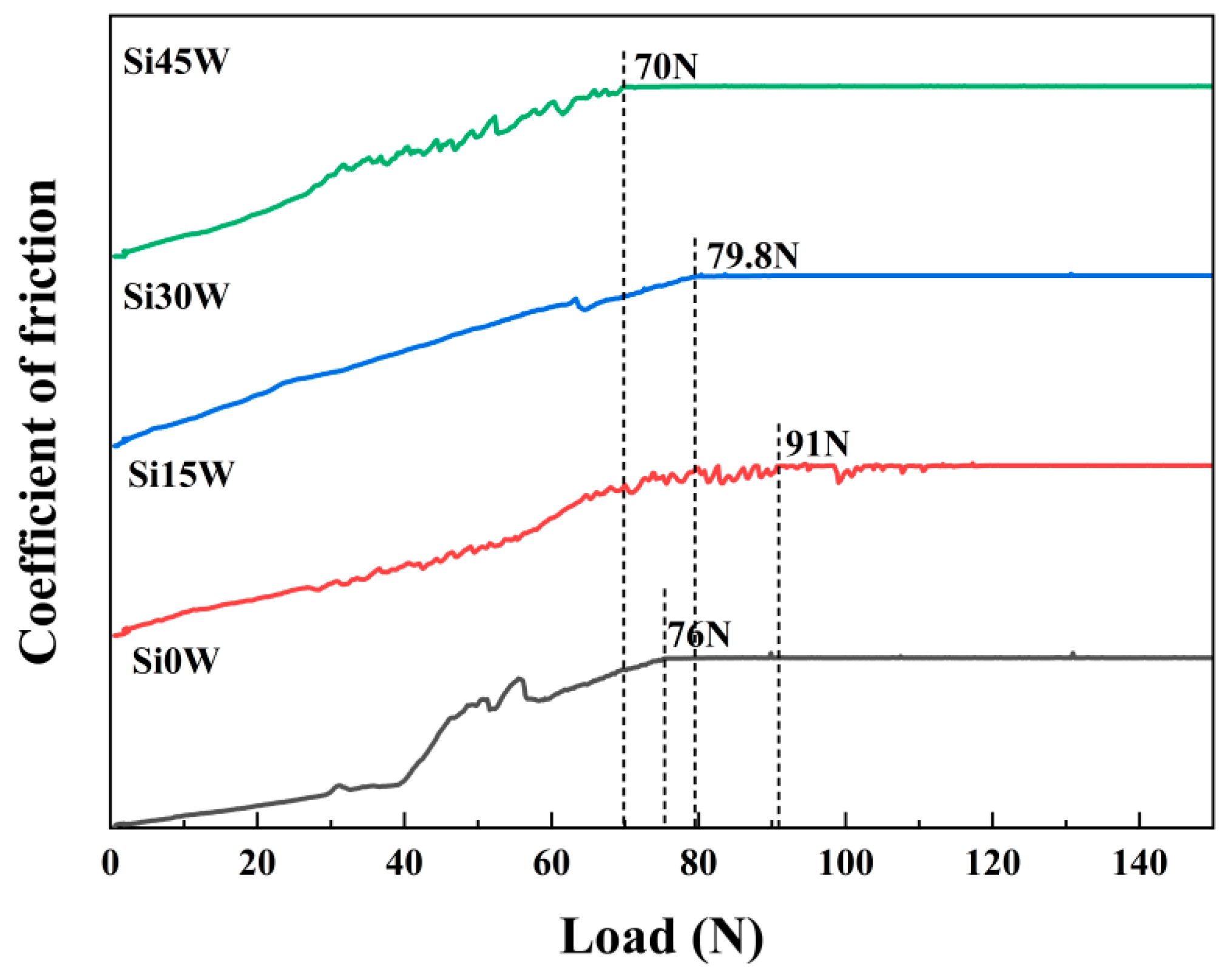
To evaluate the adhesion strength behavior of the films, scratch tests were performed. Figure 7 shows that the film-substrate adhesion strength test results for all the samples exceeded 60 N. As the Si target power gradually increased, the adhesion first tended to increase but then decreased. When the Si target power reached 15 W, the film–substrate adhesion reached a maximum value of 91 N. When the Si target power was further increased, the adhesion strength decreased, which may be associated with the increased structural disorder and amorphous contribution induced by excessive Si incorporation and the possible increase in residual stress in the films [12]. Residual stress was not quantified in the present work; therefore, this interpretation is based on the observed microstructural evolution and adhesion trend.

3.3. Tribological Properties

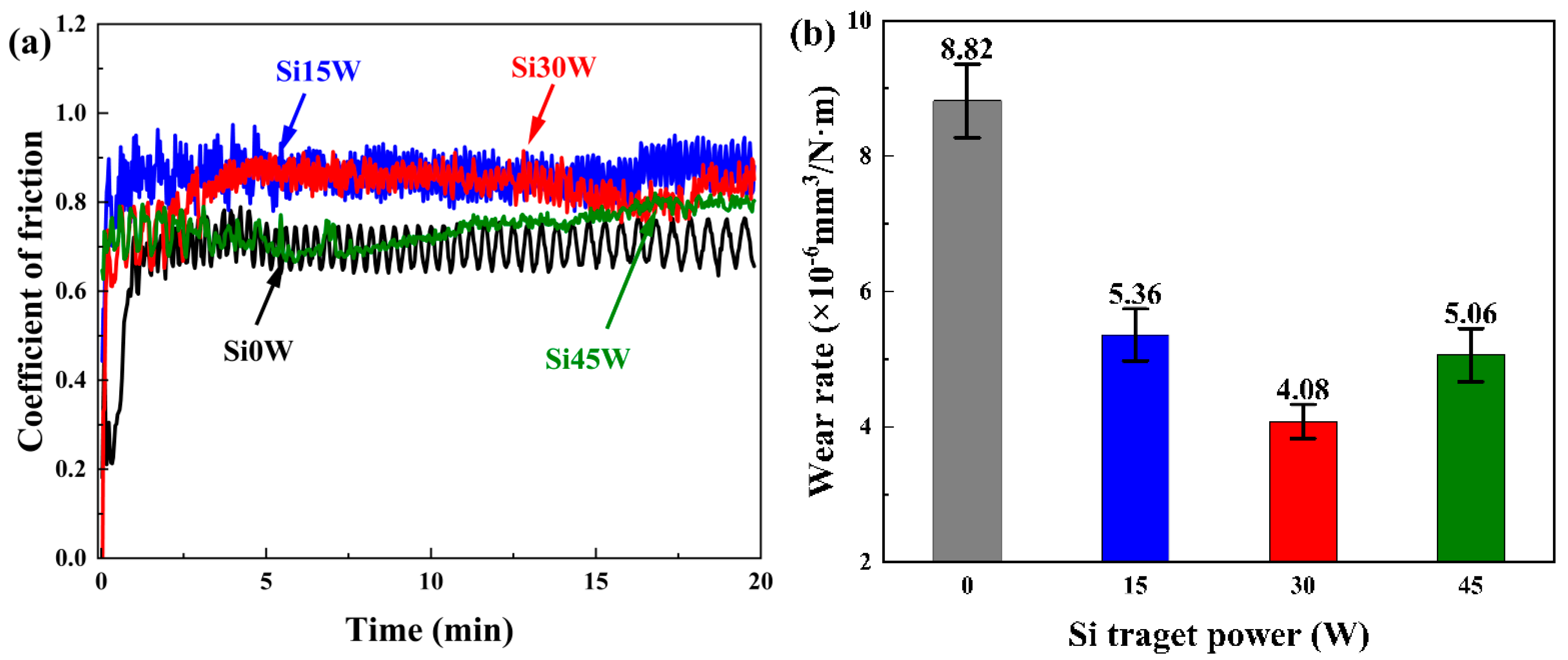
Figure 8 presents the coefficient of friction (COF) and wear rate of (WMoTaNb)SiN films prepared under different Si target powers. In the early stage of the wear test, due to the influence of the contact area and surface roughness, the COF sharply increases. After approximately 2 min, the COF gradually stabilized. The average friction coefficients of the films deposited at Si target powers of 0, 15, 30, and 45 W were measured to be 0.71, 0.85, 0.82, and 0.74 respectively. The incorporation of Si reduced the size of surface clusters and lowered surface roughness, thereby increasing the contact area between the friction pairs and the film during the wear process, substantially reducing fluctuations in the COF [11,29,31,32,34,35,36,37]. The wear rates of the films with different Si target power are shown in Figure 8b. It should be noted that the wear-rate values reported here were calculated from the film-side wear-track volume and do not include the wear of the GCr15 counterface ball. The Si30W film exhibited the lowest wear rate, indicating the best wear resistance among the tested films under the same conditions. As the power of the Si target continuously increases, the wear rate shows a significant downward trend. When the Si target power is 0, 15, 30, and 45 W, respectively, the corresponding wear rate values are 8.82 × 10⁻⁶, 5.36 × 10⁻⁶, 4.08 × 10⁻⁶, and 5.06 × 10⁻⁶ mm3/(N·m) The wear rate of the Si30W film is 46% that of the Si0W film.
It should be noted that the friction coefficient and wear rate do not necessarily exhibit the same variation trend, because they reflect different aspects of tribological response. The friction coefficient is mainly associated with the interfacial shear behavior during sliding, whereas the wear rate is more directly related to the load-bearing capacity, resistance to plastic deformation, and stability of the near-surface microstructure. Therefore, a film may exhibit a relatively higher friction coefficient but still possess a lower wear rate. In the present work, the reduced wear rate of the Si-containing films, especially the film deposited at 30 W, is primarily attributed to the improved mechanical support (higher hardness and H3/E2) and the more stable wear-track morphology, even though the friction coefficient does not decrease monotonically with increasing Si target power. In addition, although a smoother surface can reduce asperity ploughing, the friction coefficient is also strongly influenced by tribo-oxidation, transfer-layer formation, and local adhesive interactions with the GCr15 counterface; thus, a lower surface roughness does not necessarily lead to a lower friction coefficient.
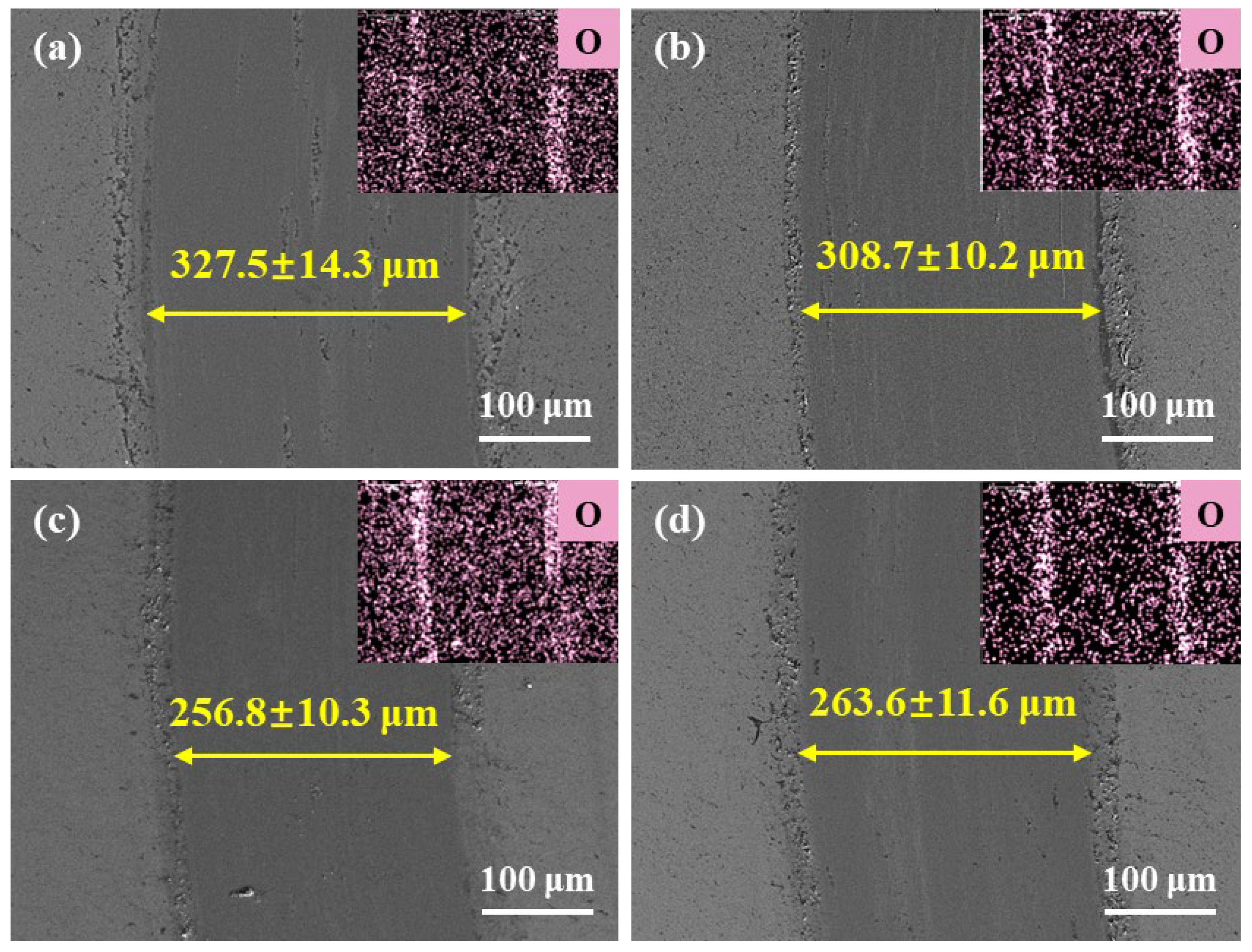
Figure 9 presents the wear track morphology and O element EDS mapping of (WMoTaNb)SiN films prepared under different Si target powers. Figure 9a shows that the Si0W film has a wear scar with a width of 327.5 μm. As the Si target power increased, the wear track width gradually decreased, reaching a minimum of 237.62 μm when the Si target power was 30 W (Figure 9c). Based on the EDS results, the oxygen content at the wear track boundaries was relatively high, suggesting that severe oxidative wear occurred during the wear process. The improvement in wear resistance correlates directly with the mechanical properties of the films. Specifically, the film deposited at Si30W presented the highest hardness (28.5 GPa) and toughness (H3/E2 value of 0.24), which could effectively reduce plastic deformation during the wear process [9,24,25,38].

3.4. High-Temperature Oxidation Resistance and Ablation Resistance

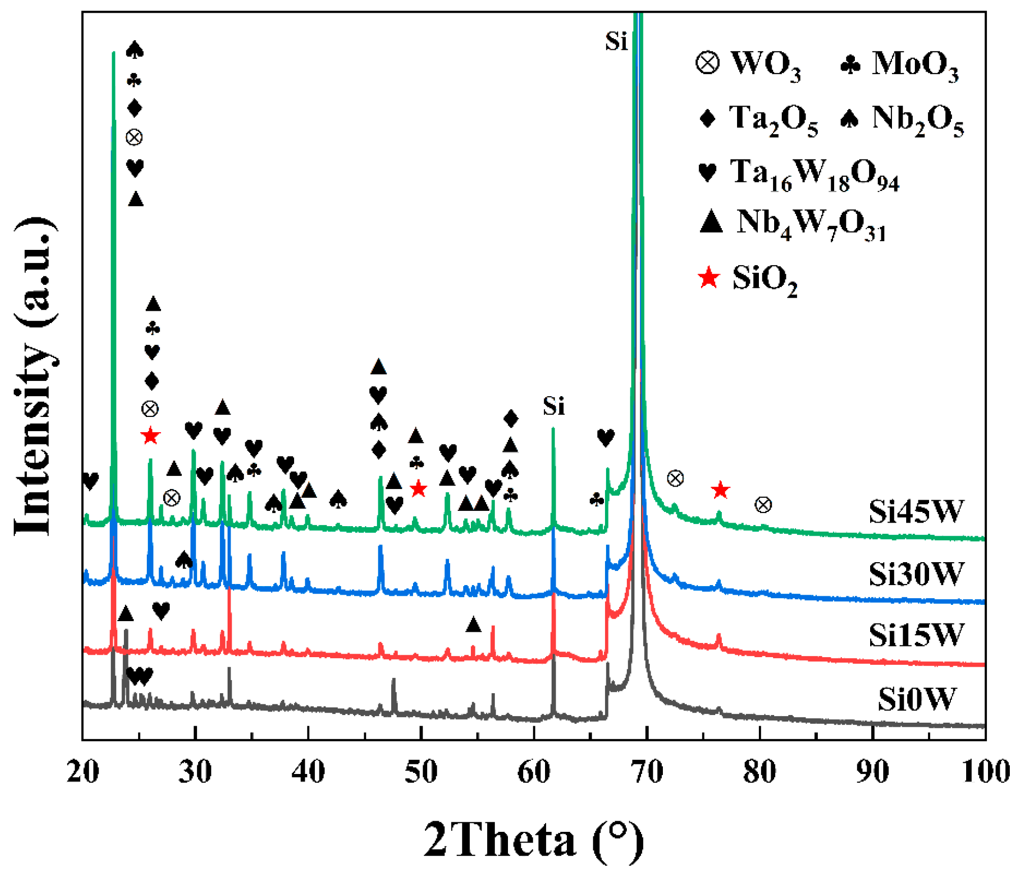
The oxidation products on the film surface after oxidation at 1000 °C for 120 min were analyzed via XRD to further determine the formation of the oxidation products of the (WMoTaNb)SiN films, as depicted in Figure 10. An oxide scale formed on the film surface, containing abundant oxides such as WO3, MoO3, Ta2O5, Nb2O5, and SiO2. Moreover, complex oxides, including Ta16W18O94 and Nb4W7O31, have also been detected [1,13,14,15,25,39,40,41,42]. For Si0W film, low-boiling MoO3 and WO3 are susceptible to evaporation during high-temperature oxidation, leading to XRD patterns dominated by Nb2O5 and Nb4W7O31. On the other hand, the intensity of the SiO2 XRD peak gradually increased with increasing Si target power. The Si-containing films presented a greater presence of diffraction peaks corresponding to Ta16W18O94 and Nb4W7O31. This can be attributed to the reactions among WO3, Ta2O5, and Nb2O5. The formation of these complex oxides (Ta16W18O94 and Nb4W7O31) consumed the preformed WO3, thereby inhibiting its evaporation. A similar redox mechanism has been reported in previous studies involving Si-containing systems [25].
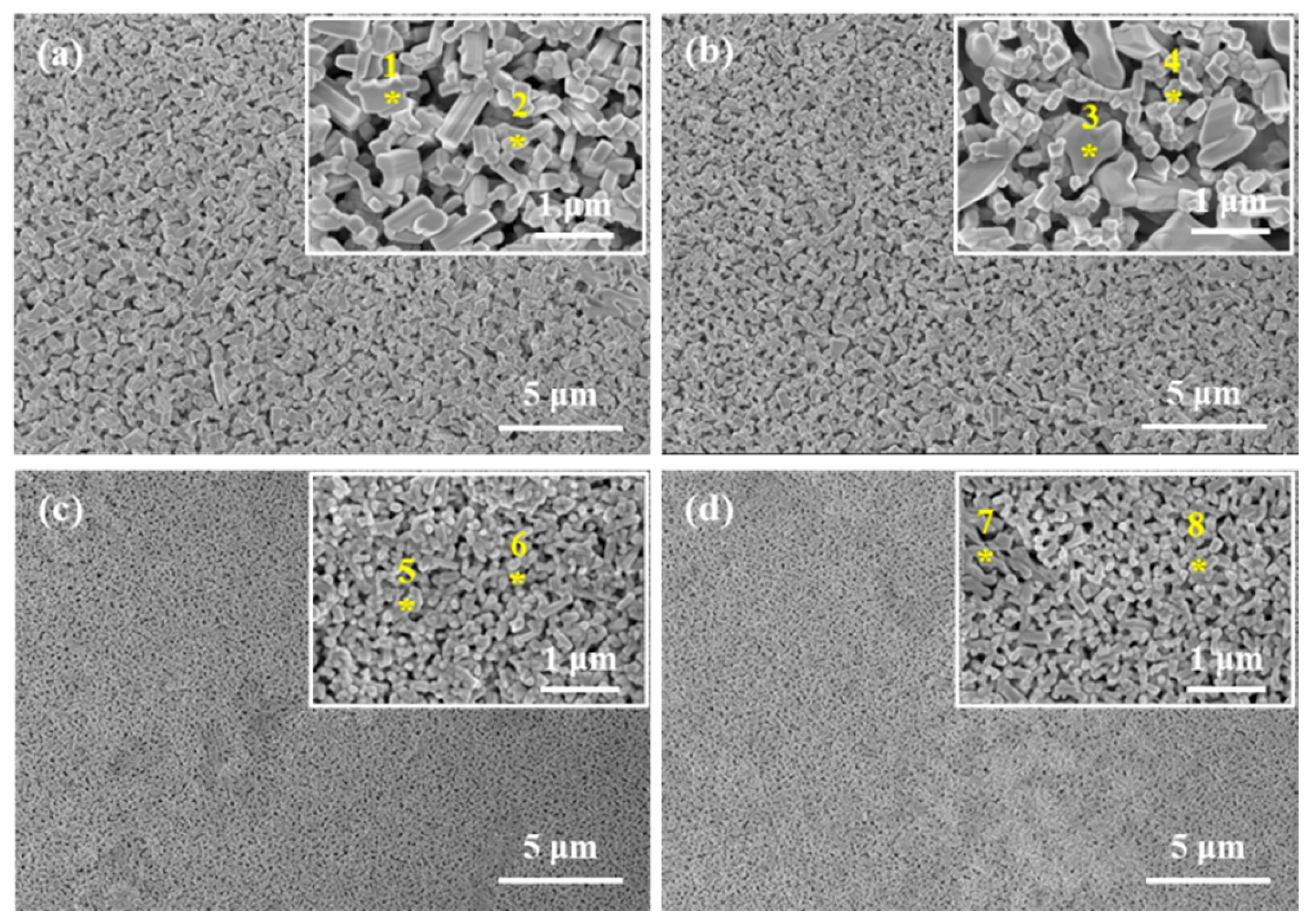
As shown in Figure 11, it depicts the surface morphology of the (WMoTaNb)SiN films after high-temperature oxidation at 1000 °C for 2 h in air. With increasing Si target power, the size of the oxides on the surface of the film tends to decrease, and the size of the pores formed by oxidation decreases significantly. Combined with the analysis in Table 2, it can be seen that the surface of the films is mainly composed of Nb- and Ta-rich oxides. The XRD analysis revealed that the oxides are mainly Ta2O5 and Nb2O5. During the oxidation process, O atoms quickly penetrate into the film through micropores, aggravating the oxidation of the films. The addition of Si will generate a SiO2 glass phase during the oxidation process, which will cover the surface of the films. SiO2 fills the holes and cracks caused by the volatilization of oxides generated by W and Mo at high temperatures during the oxidation process and forms a relatively dense SiO2 protective film on the surface of the oxide layer. It should be noted that the very low W and Mo contents detected in the post-oxidation surface EDS point analyses mainly reflect the composition of the outermost oxidized surface region, rather than the entire oxide scale or the underlying film. This surface depletion is consistent with the formation and volatilization of W- and Mo-containing oxides during oxidation at 1000 °C, especially volatile MoO3 and, to a lesser extent, WO3. However, the depletion depth of W and Mo was not quantitatively determined in the present work because no compositional depth profiling (for example, cross-sectional EDS line scan or XPS depth profiling) was performed. Based on the cross-sectional SEM observations, the compositional redistribution and depletion behavior are considered to occur predominantly within the oxide-scale region, whose thickness varies with Si target power. The results show that the Si30W and Si45W films have better oxidation resistance, whereas the Si0W and Si15W films have poor oxidation resistance. The high-temperature oxidation resistance of the films improved with increasing Si target power [43]. In this context, the oxide-scale thickness provides a geometric framework for interpreting the depletion behavior: although thicker oxide scales do not necessarily indicate lower oxidation resistance, they suggest that oxidation-induced compositional redistribution and volatilization-related depletion are confined to a larger reacted layer rather than directly representing the composition of the retained nitride film beneath. Figure 12 presents the cross-sectional morphology of the (WMoTaNb)SiN films after oxidation at 1000 °C for 2 h.
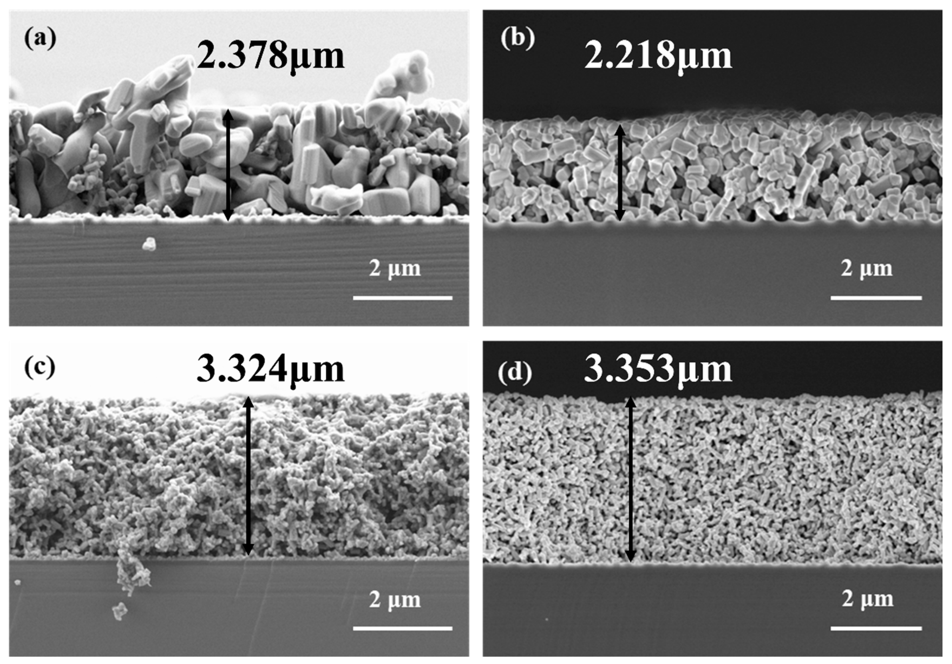
Figure 12 presents the cross-sectional morphology of the (WMoTaNb)SiN films after oxidation at 1000 °C for 2 h. As shown in Figure 12a, the Si0W film has an oxide layer approximately 2.37 μm thick on the surface. However, cracks and holes within the oxide layer permit oxygen to further diffuse into the film, leading to internal oxidation of the RHEAN films. The degree of oxidation in Si-containing films is significantly enhanced, and the oxide size of the Si30W and Si45 samples is substantially reduced. It can be concluded that the oxidation resistance increases as the Si target power increases. However, owing to the low Si target power, a dense oxide layer failed to form, which eventually led to the complete failure of the films [44,45,46].
Based on the XRD and SEM characterization results, the primary oxides formed on the film surface in this study are WO3, MoO3, Ta2O5, Nb2O5, SiO2, Ta16W18O94, and Nb4W7O31. These oxidation products align with those reported for most WMoTaNb-based alloys. Our experimental results demonstrate that the addition of an appropriate amount of Si improves the oxidation resistance of the system. As follows, we discuss the reason for this in terms of thermodynamics as well as oxidation processes. The magnitude of the standard Gibbs free energy change (ΔG) reflects the thermodynamic stability of oxides. The ΔG values of WO3, MoO3, Ta2O5, Nb2O5, and SiO2, which were calculated via HSC Chemistry 6.0 software, were calculated via Equations (1)–(5):
2W2N + 4O2(g) = 4WO2 + N2(g)
∆G = −1417.45 kJ/mol
2MoN + 3O2(g) = 2MoO3 + N2(g)
∆G = −1033.91 kJ/mol
2TaN + 2.5O2(g) = Ta2O5 + N2(g)
∆G = −1191.03 kJ/mol
2NbN + 2.5O2(g) = Nb2O5 + N2(g)
∆G = −1120.27 kJ/mol
Si3N4 + 3O2(g) = 3SiO2 + 2N2(g)
∆G = −1704.62 kJ/mol
These results show that SiO2 is preferentially formed during the oxidation process, followed by WO3, Ta2O5, Nb2O5, and MoO3. However, as oxidation progresses, Si is gradually consumed due to the formation of SiO2, leading to its depletion and failure to sustain the critical concentration required for continuous SiO2 formation. Other oxides are subsequently generated. Thus, the oxidation resistance of the films significantly increased with increasing Si target power. Due to the discontinuous and mechanically unstable oxidized surface after exposure at 1000 °C for 2 h, reliable post-oxidation nanoindentation could not be obtained; therefore, the oxidation performance is evaluated primarily based on oxide-phase constitution, surface morphology, and oxide-scale thickness.
The ablation resistance of the (WMoTaNb)SiN films was evaluated under repeated oxyhydrogen-flame exposures. The mass changes before and after the ablation cycles are presented in Table 3, showing small net mass variations that reflect the competition balance between oxidation-induced mass gain and ablation-driven material loss. The mass change was minimal for the Si0W sample, with a slight mass gain of +0.0003 g, whereas all Si-containing films exhibited net mass losses, with the Si30W film showing the largest decrease of −0.0034 g. These results indicate that the post-ablation mass variation is governed by the coupled effects of thermo-oxidation, oxide volatilization, and local material removal rather than by a single process.
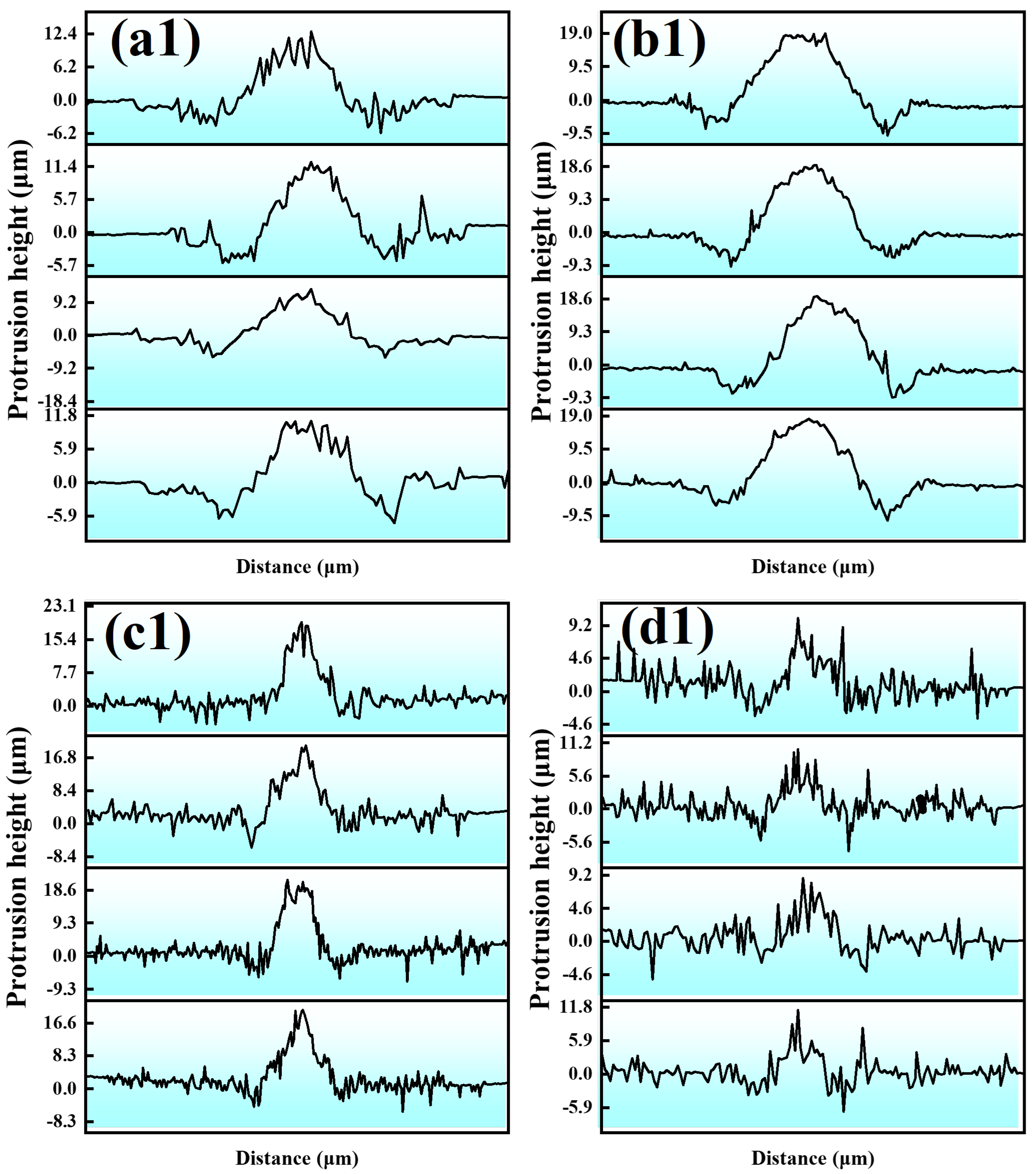
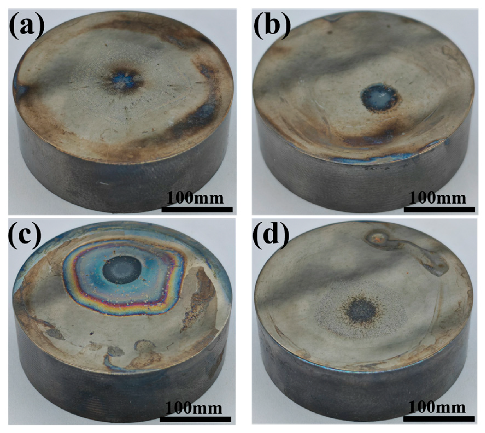
The macroscopic morphology of the ablated film is shown in Figure 13. The laser confocal curve of the ablation center area after the flame ablation is shown in Figure 14. The Si0W film exhibited a relatively uniform ablation profile, with limited topographic fluctuation, which is consistent with its stable surface morphology after repeated flame exposure. By contrast, the Si15W, Si30W, and Si45W films resulted in more pronounced material removal in the flame-impingement zone, accompanied by increasingly irregular ablation-center profiles and larger local roughness fluctuations. It should be emphasized that, in the present work, “local destruction” refers to localized film failure at the ablation center, including film removal or spallation and the consequent exposure of the substrate. Therefore, the more irregular ablation contours in the Si-containing films indicate a stronger spatial heterogeneity of the ablation response rather than simply a uniform increase in bulk material loss.
Laser confocal analysis of the ablated regions, shown in Figure 14(a1–d1), further confirms these observations. Compared with those of the Si0W and Si15W films, the ablation profiles of the Si30W and Si45W films showed deeper and wider material loss. The confocal profiles of the Si30W and Si45W films demonstrated more significant surface disruption, with peaks and valleys corresponding to localized material removal and film spallation. In contrast, the Si0W film exhibited minimal disruption, confirming its relative stability during the ablation process [47].
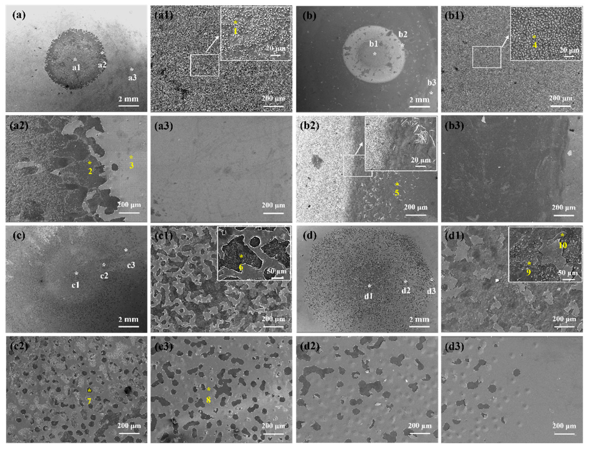
EDS analyses of the ablated regions, shown in Figure 15, revealed the pronounced presence of Fe enrichment, indicating substantial substrate exposure in the areas where the film was removed. The elemental composition after ablation shows that the Si signal in the ablated regions was significantly reduced, particularly for Si30W and Si45W samples, where Si was scarcely detected in most point-scan locations. This is the original measurement outcome and suggests that the ablated surface chemistry is dominated by oxide products and substrate-derived signals after severe flame exposure. Considering the possible spectral overlap between Si Kα and W Mα in EDS analysis, the Si-related point-scan results should be interpreted with caution in terms of absolute values. Nevertheless, the consistently weak Si signal together with Fe enrichment and the oxide-dominated compositions still supports substantial local film removal and substrate exposure in the ablation zone. This suggests that the Si-containing oxidation products, which provide protection under high-temperature oxidation conditions, were not retained effectively in the analyzed ablation regions after repeated flame exposure. In addition, Fe enrichment further confirmed the exposure of the substrate and the degradation of the film integrity [47,48,49]. The Si signal in the ablated regions was significantly reduced, with almost no Si detected in most analyzed areas. Given the possible EDS spectral overlap between Si Kα and W Mα, the Si-related point-analysis results should be interpreted with caution in terms of absolute content; however, the consistently weak Si signal together with the Fe enrichment and oxide-dominated composition still supports substantial local film removal and substrate exposure after ablation.
Point scan data from different regions of the ablated films (Table 4) further support the spatially heterogeneous ablation behavior. For the Si0W sample, the slight net mass gain indicates that oxidation-induced mass increase nearly offsets ablation-driven material loss. In contrast, the Si-containing films show net mass loss together with Fe enrichment in the ablation zone, confirming local film failure and substrate exposure. In particular, the coexistence of coated and uncoated regions in the ablation center of the Si45W sample (as reflected by the point-scan positions selected from film-covered and film-free areas) demonstrates that local destruction proceeds in a non-uniform manner under repeated oxyhydrogen-flame loading. The reduced Si signal after ablation, especially in Si30W and Si45W, indicates that the contribution of Si-containing surface products becomes limited in the analyzed ablation zones after severe thermo-mechanical damage.
The degradation of the films during ablation is dominated by a combination of intense thermal flux, rapid oxidation, oxide-scale evolution, and cyclic thermo-mechanical damage. For Si0W, the negligible net mass change and relatively uniform ablation profile suggest that oxidation and material removal remain near-balanced over the tested cycles. However, for the Si-containing films, particularly Si30W and Si45W, the ablation environment involves much steeper thermal gradients and repeated transient thermal shocks than the static oxidation test, which can promote local cracking, spallation, and removal of the oxide scale and near-surface film material.
Laser confocal and SEM observations of the ablated regions indicate that the ablation-induced damage is more severe in the Si30W and Si45W films. This does not contradict their superior mechanical properties and oxidation resistance under the corresponding tests; instead, it indicates that oxidation resistance under static high-temperature exposure cannot be directly extrapolated to flame-ablation conditions, where oxide-scale stability under transient thermo-mechanical loading becomes critical. The larger local material removal in these films is therefore associated with the failure and detachment of the ablation-affected surface layer, followed by localized substrate exposure.
The results highlight that while Si incorporation improves the mechanical and tribological performance of (WMoTaNb)SiN films, the ablation response is controlled by a balance among oxidation-product formation, oxide-scale stability, and resistance to thermo-mechanical damage under repeated flame impingement. Therefore, optimizing Si target power is essential to achieve a better compromise among oxidation resistance, wear resistance, and ablation tolerance under extreme thermal conditions.
The surface temperature during oxyhydrogen-flame exposure was not monitored in real time in the present work; therefore, the ablation behavior was evaluated primarily based on post-test mass change, macroscopic morphology, laser confocal profiles, and SEM/EDS characterizations.
Overall, the present results demonstrate that tuning the Si target power effectively regulates the microstructural evolution and, consequently, the mechanical, tribological, oxidation, and ablation responses of magnetron-sputtered (WMoTaNb)SiN films, while also highlighting the trade-off between improved oxidation-related protection and oxide-scale stability under severe flame-ablation conditions. To ensure a rigorous interpretation of these findings, several limitations should be acknowledged. First, the residual stress of the films was not directly quantified, and thus the discussion of adhesion degradation at higher Si target power in relation to structural disorder and possible stress buildup remains inferential. Second, although the XRD results indicate mixed crystalline features and an amorphous contribution, the crystalline-to-amorphous phase fractions and nanocrystallite size were not directly quantified by TEM-based characterization. Third, because of the spectral overlap between Si Kα and W Mα lines, the absolute quantification of Si by EDS in W-containing regions carries uncertainty; therefore, Si-related EDS data are interpreted primarily as relative compositional trends and supportive evidence. Finally, the ablation process was evaluated without real-time surface-temperature monitoring or in situ oxide-scale diagnostics, so the ablation mechanism analysis is based on post-test evidence, including mass change, macroscopic morphology, laser confocal profiles, and SEM/EDS characterizations. Despite these limitations, the comparative trends obtained under consistent experimental conditions provide a reliable basis for understanding the effect of Si target power on the multi-performance balance of (WMoTaNb)SiN films.

4. Conclusions

In this study, a series of (WMoTaNb)SiN films were successfully deposited by magnetron co-sputtering under different Si target powers, and the effects of Si target power on the microstructure and multi-performance responses of the films were systematically investigated. The main conclusions are summarized as follows:
(1)
The as-deposited (WMoTaNb)SiN films exhibited typical columnar growth structures in all samples, while the microstructural compactness and refinement changed with Si target power. When the Si target power increased from 0 to 45 W, the surface features became finer and the cross-sectional structure became more compact overall, accompanied by an increase in film thickness and deposition rate. These changes are attributed to the Si-target-power-dependent deposition kinetics and microstructural evolution during film growth, rather than a structural transition from disorder to columnar growth.
(2)
When the Si target power was 30 W, the film exhibited the highest hardness (28.5 GPa), the highest elastic modulus (303.4 GPa), the maximum H3/E2 value, and the lowest film-side wear rate (4.08 × 10⁻⁶ mm3·N−1·m−1) under sliding against a GCr15 steel ball, indicating the best overall mechanical and tribological performance among the tested films. The wear-rate comparison reported in this work is based on the wear-track volume loss of the film side (the wear of the GCr15 counterface ball was not included), and the performance improvement at 30 W is associated with the favorable balance among microstructural compactness, resistance to plastic deformation, and tribo-oxidation-assisted surface protection under the present test conditions.
(3)
The oxidation and ablation responses were strongly dependent on Si target power. During oxidation at 1000 °C in air for 2 h, Si-containing films promoted the formation of SiO2-containing oxide scales and showed more compact surface oxidation products than Si0W, while the oxide-scale thickness and morphology indicated that oxidation resistance should be evaluated by considering both scale compactness and reacted-layer characteristics. Because the Si Kα and W Mα lines overlap in EDS analysis, Si-related EDS values in W-containing regions were interpreted mainly as comparative trends rather than strict absolute quantification; the oxidation and ablation conclusions were therefore established from combined evidence, including XRD, SEM morphologies, compositional evolution, mass change, and laser confocal profiles. During repeated oxyhydrogen-flame ablation, the post-test mass change remained very small in magnitude, indicating competition between oxidation-induced mass gain and ablation-driven material loss. Under the present ablation conditions, the ablation response was governed by the coupled effects of oxide formation, oxide-scale stability, and thermo-mechanical damage, and the Si30W film showed the best overall balance of mechanical, tribological, oxidation, and ablation-related performance in this study.

Author Contributions

X.W.: Writing—review & editing, Writing—original draft, Validation, Methodology, Investigation, Data curation, Conceptualization, Formal analysis. S.W.: Writing—review & editing, Formal analysis, Methodology. W.S.: Writing—review & editing, Methodology, Funding acquisition, Conceptualization, Supervision. J.C.: Validation, Investigation, Data curation. W.Y.: Resources, Data curation, Funding acquisition, Validation, Writing—review & editing. All authors have read and agreed to the published version of the manuscript.

Funding

This research was funded by the National Natural Science Foundation of China (No. U24A2034, 52271112, U24A20106), the Scientific Research Program funded by Shaanxi Provincial Education Department (No. 24JP083), Shaanxi Provincial Science & Technology Department (Nos. 2023KXJ-105, QCYRCXM-2022-303, 2024CY2-GJHX-61), Shaanxi Laboratory of Advanced Materials (No. 2024ZY-JCYJ-04-11), Innovation Capability Support Program of Shaanxi (No. 2024RS-CXTD-61), Key Research and Development Program of Shaanxi (No. 2024QY2-GJHX-24, 2024CY2-GJHX-40, No. 2025CY-GJHX-01). And The APC was funded by the National Natural Science Foundation of China (No. U24A2034, 52271112, U24A20106).

Institutional Review Board Statement

Not applicable.

Informed Consent Statement

Not applicable.

Data Availability Statement

Data will be made available on request.

Conflicts of Interest

The authors declare no conflicts of interest.

References

  1. Gorr, B.; Schellert, S.; Müller, F.; Christ, H.; Kauffmann, A.; Heilmaier, M. Current status of research on the oxidation behavior of refractory high entropy alloys. Adv. Eng. Mater. 2021, 23, 2001047. [Google Scholar] [CrossRef]
  2. Senkov, O.; Wilks, G.; Miracle, D.; Chuang, C.; Liaw, P. Refractory high-entropy alloys. Intermetallics 2010, 18, 1758–1765. [Google Scholar] [CrossRef]
  3. Senkov, O.N.; Isheim, D.; Seidman, D.N.; Pilchak, A.L. Development of a refractory high entropy superalloy. Entropy 2016, 18, 102. [Google Scholar] [CrossRef]
  4. Senkov, O.N.; Miracle, D.B.; Chaput, K.J.; Couzinie, J. Development and exploration of refractory high entropy alloys—A review. J. Mater. Res. 2018, 33, 3092–3128. [Google Scholar] [CrossRef]
  5. Song, H.; Tian, F.; Wang, D. Thermodynamic properties of refractory high entropy alloys. J. Alloys Compd. 2016, 682, 773–777. [Google Scholar] [CrossRef]
  6. Xie, X.; Li, N.; Liu, W.; Huang, S.; He, X.; Yu, Q.; Xiong, H.; Wang, E.; Hou, X. Research progress of refractory high entropy alloys: A review. Chin. J. Mech. Eng. 2022, 35, 142. [Google Scholar] [CrossRef]
  7. Xiong, W.; Guo, A.X.; Zhan, S.; Liu, C.; Cao, S. Refractory high-entropy alloys: A focused review of preparation methods and properties. J. Mater. Sci. Technol. 2023, 142, 196–215. [Google Scholar] [CrossRef]
  8. Zhang, J.; Li, Z.; Ma, Y.; Guo, N.; Liu, J.; Yuan, S.; Ma, Z.; Yang, H. Refractory high-entropy alloys: A focused review of high-temperature properties and deformation mechanisms. Mater. Charact. 2025, 227, 115250. [Google Scholar] [CrossRef]
  9. Li, Y.; Zhang, C.; Peng, S.; Zheng, J.; Cui, X.; Zhang, S.; Sun, D. Effect of nitrogen flow rate on the thermal stability and wear resistance of (AlCrTiZrSi)Nx high-entropy nitride coatings. Ceram. Int. 2025, 51, 12396–12407. [Google Scholar] [CrossRef]
  10. Lu, X.; Zhang, X.; Lu, Y.; Wang, C.; Hao, J.; Liu, W. Characterization and wear role of (CrAlVTiNb)Nx high-entropy alloy nitride films deposited by high power impulse magnetron sputtering. J. Alloys Compd. 2025, 1020, 179395. [Google Scholar] [CrossRef]
  11. Yang, W.; Shen, J.; Wang, Z.; Ma, G.; Ke, P.; Wang, A. Mechanical and electrochemical properties of (MoNbTaTiZr)1-xNx high-entropy nitride coatings. J. Mater. Sci. Technol. 2025, 208, 78–91. [Google Scholar] [CrossRef]
  12. Wu, S.; Shao, W.; Yang, W.; Gao, W.; Chen, J.; Ding, R. Effect of working pressure on microstructure, mechanical properties and tribology performance of (SiTiVNbCr)N high entropy nitride films. Tribol. Int. 2025, 214, 111308. [Google Scholar] [CrossRef]
  13. Locherer, K.; Salje, E. The refinement of a tetragonal phase of WO3 using a novel PSD high temperature X-ray powder diffractometer. Phase Transit. 1999, 69, 85–93. [Google Scholar] [CrossRef]
  14. Lu, S.; Li, X.; Liang, X.; He, J.; Shao, W.; Li, K.; Chen, J. Effect of Y additions on the oxidation behavior of vacuum arc melted refractory high-entropy alloy AlMo0.5NbTa0.5TiZr at elevated temperatures. Vacuum 2022, 201, 111069. [Google Scholar] [CrossRef]
  15. Lu, S.; Li, X.; Liang, X.; Shao, W.; Yang, W.; Chen, J. Effect of Al content on the oxidation behavior of refractory high-entropy alloy AlMo0.5NbTa0.5TiZr at elevated temperatures. Int. J. Refract. Met. Hard Mater. 2022, 105, 105812. [Google Scholar] [CrossRef]
  16. Moghaddam, A.O.; Sudarikov, M.; Shaburova, N.; Zherebtsov, D.; Zhivulin, V.; Solizoda, I.A.; Starikov, A.; Veselkov, S.; Samoilova, O.; Trofimov, E. High temperature oxidation resistance of W-containing high entropy alloys. J. Alloys Compd. 2022, 897, 162733. [Google Scholar] [CrossRef]
  17. Müller, F.; Gorr, B.; Christ, H.-J.; Chen, H.; Kauffmann, A.; Heilmaier, M. Effect of microalloying with silicon on high temperature oxidation resistance of novel refractory high-entropy alloy Ta-Mo-Cr-Ti-Al. Mater. High Temp. 2018, 35, 168–176. [Google Scholar] [CrossRef]
  18. Diyatmika, W.; Cheng, C.Y.; Lee, J.W. Fabrication of Cr-Si-N coatings using a hybrid high-power impulse and radio-frequency magnetron co-sputtering: The role of Si incorporation and duty cycle. Surf. Coat. Technol. 2020, 403, 126378. [Google Scholar] [CrossRef]
  19. Tsai, D.C.; Chang, Z.C.; Kuo, P.S.; Chen, E.-C.; Huang, Y.L.; Shieu, F.-S. Si-target power dependence on the microstructure, mechanical behavior, and electro-optical characteristics of magnetron sputtered Six(TiZrHf)1-xN coatings. J. Mater. Res. Technol. 2023, 22, 35–53. [Google Scholar] [CrossRef]
  20. Das, C.R.; Rangwala, M.; Ghosh, A. Effect of Si contents on microstructure and mechanical characteristics of TiAlSiN thin film deposited by HiPIMS using different Ti-Si target compositions. Surf. Coat. Technol. 2024, 476, 130212. [Google Scholar] [CrossRef]
  21. Hu, Y.; Wang, S.; Chai, L.; Wang, P.; Li, Y. Effect of power on the microstructure and frictional properties of Si-DLC films prepared by high-power impulse magnetron sputtering (HiPIMS). Surf. Coat. Technol. 2025, 513, 132513. [Google Scholar] [CrossRef]
  22. Lü, W.; Li, G.; Zhou, Y.; Liu, S.; Wang, K.; Wang, Q. Effect of high hardness and adhesion of gradient TiAlSiN coating on cutting performance of titanium alloy. J. Alloys Compd. 2020, 820, 153137. [Google Scholar] [CrossRef]
  23. Tillmann, W.; Dildrop, M. Influence of Si content on mechanical and tribological properties of TiAlSiN PVD coatings at elevated temperatures. Surf. Coat. Technol. 2017, 321, 448–454. [Google Scholar] [CrossRef]
  24. Liu, Y.; Zhang, Y.; Zhang, H.; Wang, N.; Chen, X.; Zhang, H.; Li, Y. Microstructure and mechanical properties of refractory HfMo0.5NbTiV0.5Six high-entropy composites. J. Alloys Compd. 2017, 694, 869–876. [Google Scholar] [CrossRef]
  25. Coh, S.; Vanderbilt, D. Structural stability and lattice dynamics of SiO2 cristobalite. Phys. Rev. B—Condens. Matter Mater. Phys. 2008, 78, 054117. [Google Scholar] [CrossRef]
  26. Xu, Q.; Wang, Q.; Chen, D.-z.; Fu, Y.-a.; Shi, Q.-s.; Yin, Y.-j.; Zhang, S.-y. Microstructure characteristics and mechanical properties of NbMoTiVWSix refractory high-entropy alloys. China Foundry 2022, 19, 495–502. [Google Scholar] [CrossRef]
  27. Xu, Z.; Ma, Z.; Tan, Y.; Wang, M.; Zhao, Y.; Cheng, X. Effects of Si additions on microstructures and mechanical properties of VNbTiTaSix refractory high-entropy alloys. J. Alloys Compd. 2022, 900, 163517. [Google Scholar] [CrossRef]
  28. Li, Z.; Pang, J.; Liu, H.; Zhu, Z.; Zhang, L.; Wang, A.; Li, W.; Zhang, H.; Zhang, H. Combined effect of silicon doping and thermal treatment on microstructures and mechanical properties of Ti50Nb20V20Al10 refractory high-entropy alloy. J. Alloys Compd. 2024, 1005, 176075. [Google Scholar] [CrossRef]
  29. Senkov, O.; Scott, J.; Senkova, S.; Miracle, D.; Woodward, C. Microstructure and room temperature properties of a high-entropy TaNbHfZrTi alloy. J. Alloys Compd. 2011, 509, 6043–6048. [Google Scholar] [CrossRef]
  30. Senkov, O.; Senkova, S.; Miracle, D.; Woodward, C. Mechanical properties of low-density, refractory multi-principal element alloys of the Cr–Nb–Ti–V–Zr system. Mater. Sci. Eng. A 2013, 565, 51–62. [Google Scholar] [CrossRef]
  31. Senkov, O.; Senkova, S.; Woodward, C. Effect of aluminum on the microstructure and properties of two refractory high-entropy alloys. Acta Mater. 2014, 68, 214–228. [Google Scholar] [CrossRef]
  32. Senkov, O.N.; Wilks, G.B.; Scott, J.M.; Miracle, D.B. Mechanical properties of Nb25Mo25Ta25W25 and V20Nb20Mo20Ta20W20 refractory high entropy alloys. Intermetallics 2011, 19, 698–706. [Google Scholar] [CrossRef]
  33. Li, K.; Shao, W.; Wen, R.; Yang, W.; Wu, S.; Chen, J. A novel strategy of high-entropy nitride coating for cemented carbide cutting tool: Preparation, microstructure, mechanical and wear properties. Int. J. Refract. Met. Hard Mater. 2025, 136, 107644. [Google Scholar] [CrossRef]
  34. Bisht, A.K.; Vaishya, R.O.; Walia, R.; Singh, G. Nitrides ceramic coatings for tribological applications: A journey from binary to high-entropy compositions. Ceram. Int. 2024, 50, 8553–8585. [Google Scholar] [CrossRef]
  35. Chen, Z.; Zhang, G.; Chen, J.; Guo, C.; Sun, W.; Yang, Z.; Li, H.; Jiang, F.; Han, B. Microstructure and wear property of WMoTaNb refractory high entropy alloy coating by laser cladding. J. Mater. Res. Technol. 2024, 28, 1557–1569. [Google Scholar] [CrossRef]
  36. Feuerbacher, M.; Lienig, T.; Thomas, C. A single-phase bcc high-entropy alloy in the refractory Zr-Nb-Ti-V-Hf system. Scr. Mater. 2018, 152, 40–43. [Google Scholar] [CrossRef]
  37. Wang, Y.; Li, P.; Ma, N.; Zhang, B.; Wei, Y.; Zhang, L.; Wang, J.; Liu, S. Effect of Y2O3 on the microstructure and tribology property of WMoTaNb refractory high entropy alloy coating prepared by laser cladding. Int. J. Refract. Met. Hard Mater. 2023, 115, 106273. [Google Scholar] [CrossRef]
  38. Zhang, Y.; Liu, Y.; Li, Y.; Chen, X.; Zhang, H. Microstructure and mechanical properties of a refractory HfNbTiVSi0.5 high-entropy alloy composite. Mater. Lett. 2016, 174, 82–85. [Google Scholar] [CrossRef]
  39. Groult, D.; Pannetier, J.; Raveau, B. Neutron diffraction study of the defect pyrochlores TaWO5.5, HTaWO6, H2Ta2O6, and HTaWO6·H2O. J. Solid State Chem. 1982, 41, 277–285. [Google Scholar] [CrossRef]
  40. Liu, X.; Han, X.; Zhang, Z.; Ji, L.; Jiang, Y. The crystal structure of high temperature phase Ta2O5. Acta Mater. 2007, 55, 2385–2396. [Google Scholar] [CrossRef]
  41. Wei, W.; Wang, T.; Wang, C.; Wu, M.; Nie, Y.; Peng, J. Ductile W0.4MoNbxTaTi refractory high-entropy alloys with excellent elevated temperature strength. Mater. Lett. 2021, 295, 129753. [Google Scholar] [CrossRef]
  42. Yong, L.; Bin, L.; Jia-wen, W.; Meng, D. Effects of Al and Mo on high temperature oxidation behavior of refractory high entropy alloys. Trans. Nonferrous Met. Soc. China 2019, 29, 1476–1483. [Google Scholar] [CrossRef]
  43. Sun, J.; Lin, Z.; Qin, B.; Su, F.; Zhang, Y.; Wang, H. Effect of Si content on the microstructure and high temperature oxidation resistance of TiAlCrNiSi high-entropy alloy films synthesized by multi-target magnetron co-sputtering. J. Alloys Compd. 2024, 970, 172674. [Google Scholar] [CrossRef]
  44. Chang, Y.; Cheng, H.; Jin, X.; Li, Z.; Zhao, Q.; Wang, X.; Luo, H. Effect of Si on the corrosion resistance of AlZrNbTi lightweight refractory high-entropy alloys in acidic environment. Corros. Sci. 2024, 238, 112377. [Google Scholar] [CrossRef]
  45. Yi, H.; Yang, X.; Yang, Y.; Yin, B.; Hu, J.; Liang, M.; Yue, J.; Yin, F. New insights in the oxidation behavior of (FeCoCrNi)94Al4Ti2Six high entropy alloys at 1100 °C. Corros. Sci. 2024, 227, 111673. [Google Scholar] [CrossRef]
  46. Wang, S.Q.; Chen, L.; Yang, B.; Chang, K.K.; Du, Y.; Li, J.; Gang, T. Effect of Si addition on microstructure and mechanical properties of Ti–Al–N coating. Int. J. Refract. Met. Hard Mater. 2010, 28, 593–596. [Google Scholar] [CrossRef]
  47. Kang, P.; Liu, H.; Yang, W.; Wang, W.; Zhang, N.; Zhao, Q.; Mula, S.; Wu, G. Microstructure and ablation behavior of SiMo/graphite composites with excellent short-time ablation resistance. Corros. Sci. 2020, 168, 108590. [Google Scholar] [CrossRef]
  48. Tang, C.; Wang, D.; Sun, P.; Lai, T.; Zhang, H.; Zhou, J.; Ren, G. The CuNb alloys prepared by laser directed energy deposition: Effect of Ti addition on microstructure and properties. Int. J. Refract. Met. Hard Mater. 2025, 130, 107152. [Google Scholar] [CrossRef]
  49. Kuang, J.; Wang, Q.; Jia, Z.; Yi, G.; Sun, B.; Yang, Y.; Sun, L.; Zhang, P.; He, P.; Xing, Y. Ablation-resistant yttrium-modified high-entropy refractory metal silicide (NbMoTaW)Si2 coating for oxidizing environments up to 2100 °C. Mater. Today 2024, 80, 156–166. [Google Scholar] [CrossRef]
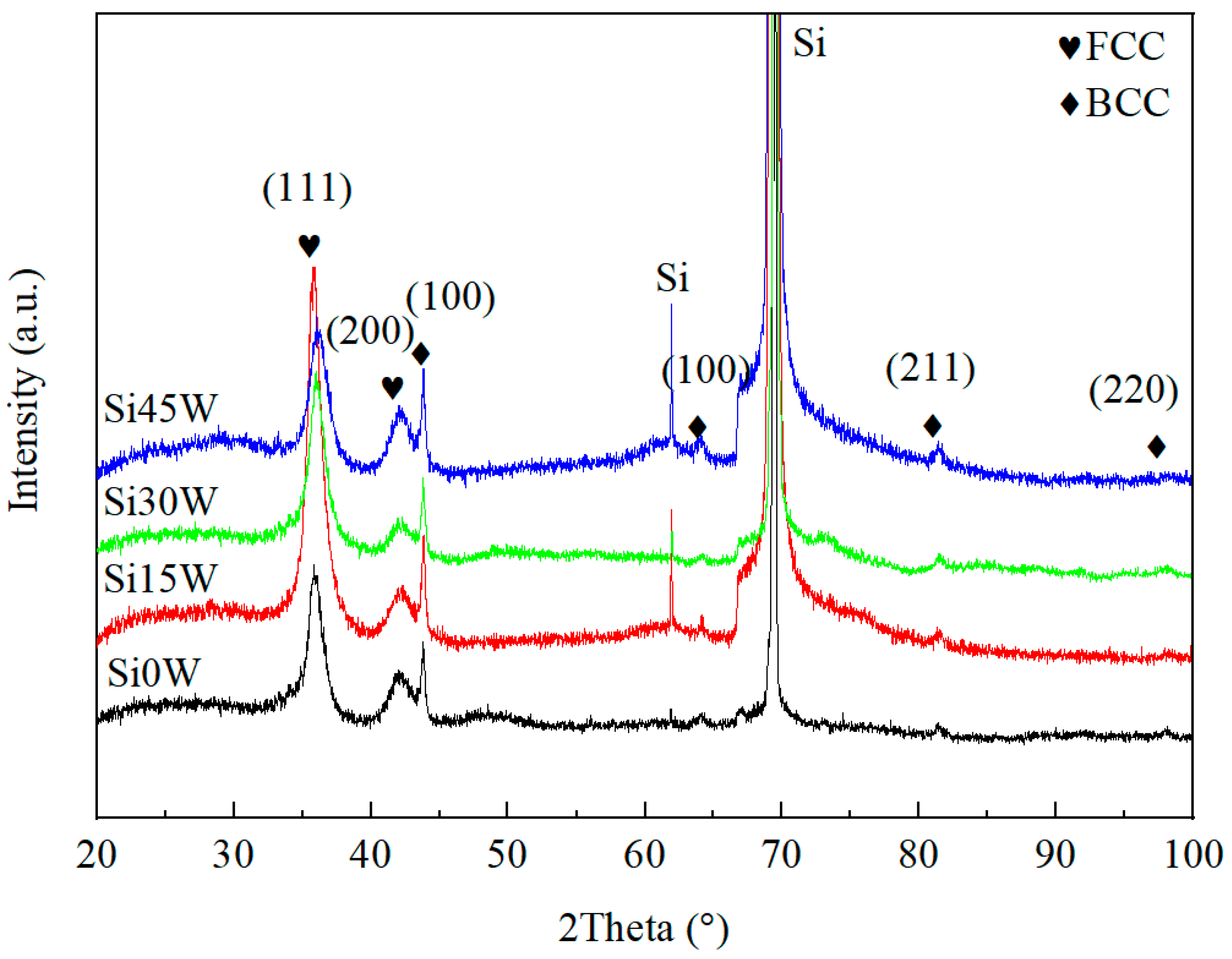
Figure 1. X-ray diffraction patterns of (WMoTaNb)SiN films deposited under different Si target powers.
Coatings 16 00309 g001
Figure 2. SEM images of the surface and cross-sectional morphologies of the (WMoTaNb)SiN films: (a,e) Si0W, (b,f) Si15W, (c,g) Si30W, and (d,h) Si45W.
Coatings 16 00309 g002
Figure 3. EDS elemental maps of the region shown in Figure 2h.
Coatings 16 00309 g003
Figure 4. Elemental composition of (WMoTaNb)SiN films deposited at different Si target powers.
Coatings 16 00309 g004
Figure 5. Load-displacement curves of (WMoTaNb)SiN films prepared at different Si target powers.
Coatings 16 00309 g005
Figure 6. (a) Hardness (H) and elastic modulus (E), (b) H/E and H3/E2 of the (WMoTaNb)SiN films prepared under different Si target powers.
Coatings 16 00309 g006
Figure 7. Adhesion strength of (WMoTaNb)SiN films prepared under different Si target powers.
Coatings 16 00309 g007
Figure 8. (a) Coefficient of friction and (b) wear rate of (WMoTaNb)SiN films prepared under different Si target powers.
Coatings 16 00309 g008
Figure 9. SEM micrographs and O element EDS analysis of the worn surfaces of (WMoTaNb)SiN films prepared under different Si target power: (a) Si0W, (b) Si15W, (c) Si30W, (d) Si45W.
Coatings 16 00309 g009
Figure 10. XRD patterns of (WMoTaNb)SiN films after high-temperature oxidation at 1000 °C for 2 h in air.
Coatings 16 00309 g010
Figure 11. Surface morphologies of the (WMoTaNb)SiN films after oxidation at 1000 °C for 2 h: (a) Si0W, (b) Si15W, (c) Si30W, (d) Si45W.
Coatings 16 00309 g011
Figure 12. Cross-sectional morphologies of the (WMoTaNb)SiN films after oxidation at 1000 °C for 2 h: (a) Si0W, (b) Si15W, (c) Si30W, and (d) Si45W.
Coatings 16 00309 g012
Figure 13. The macroscopic morphology of (WMoTaNb)SiN films deposited under different Si target powers after 8 cycles of oxyhydrogen-flame ablation: (a) Si0W, (b) Si15W, (c) Si30W, (d) Si45W.
Coatings 16 00309 g013
Figure 14. The ablation contours of (WMoTaNb)SiN films deposited under different Si target powers after 8 cycles of oxyhydrogen-flame ablation: (a1) Si0W, (b1) Si15W, (c1) Si30W, (d1) Si45W.
Coatings 16 00309 g014
Figure 15. SEM images and EDS analyses of (WMoTaNb)SiN films after 8 cycles of oxyhydrogen-flame ablation: (a,a1a3) Si0W, (b,b1b3) Si15W, (c,c1c3) Si30W, and (d,d1d3) Si45W.
Coatings 16 00309 g015
Table 1. Deposition parameters of the (WMoTaNb)SiN films.
ParametersValues
Background pressure (Pa)2.5 × 10⁻³
Working pressure (Pa)1.0
Input gas of Ar (sccm)6
Input gas N2 (sccm)2
WMoTaNb target power (W)200
Si target power (W)0, 15, 30, 45
Deposition time (min)180
Substrate temperature (°C)300
Substrate DC bias (V)−250
Rotation speed (rpm)5
Table 2. Elemental compositions of the different worn areas in Figure 11.
Elements
(at%)
Areas
12345678
W1.731.550.721.762.823.942.752.79
Mo0.000.000.000.000.000.000.000.00
Ta4.967.374.164.803.364.974.803.67
Nb5.157.474.004.833.955.545.374.37
Si--1.661.891.501.672.451.59
N2.910.005.060.005.274.723.703.68
O85.2583.6184.486.7383.179.1680.9383.9
Table 3. Mass change of (WMoTaNb)SiN films after oxyhydrogen-flame ablation.
Si Target Power (W)0153045
Before ablation (g)54.896454.772954.776154.9456
After ablation (g)54.896754.770954.772754.9449
Weight change (g)0.0003−0.002−0.0034−0.0007
Table 4. Elemental compositions of the different worn areas in Figure 15.
Elements
(at%)
Areas
12345678910
W56.4017.8049.600.000.000.000.002.500.000.00
Mo0.000.0050.400.000.000.004.004.704.2354.14
Ta43.6015.300.000.101.700.000.002.5039.8710.75
Nb0.0066.900.000.0072.100.406.904.906.5635.11
Si0.000.000.000.000.000.000.001.670.000.00
N0.000.000.000.000.000.000.0032.500.000.00
O0.000.000.0052.000.0086.8063.8028.5037.960.00
Fe0.000.000.0047.9026.2012.8025.308.2011.370.00
Disclaimer/Publisher’s Note: The statements, opinions and data contained in all publications are solely those of the individual author(s) and contributor(s) and not of MDPI and/or the editor(s). MDPI and/or the editor(s) disclaim responsibility for any injury to people or property resulting from any ideas, methods, instructions or products referred to in the content.