


Abstract
With the increasingly prominent issues of energy shortage and environmental pollution, the development of clean energy materials has become a core topic in the academic community. SnSe, as a material with moderate bandgap, a high light absorption coefficient, and environmental friendliness, has shown broad application prospects in the fields of photovoltaics and thermoelectrics. However, pure SnSe thin films have inherent defects, low carrier concentration, and high recombination rates, which limit their photoelectric conversion efficiency. This article provides a detailed overview of the characteristics of band engineering control technology, defect control technology, and carrier concentration control technology, as well as the improvements in the characteristics of SnSe thin films that they bring. This article systematically reviews the research progress on doping control technology for SnSe thin films characteristics in recent years and analyzes and discusses the differences in typical doping elements on SnSe thin films characteristics, such as optical bandgap and absorption coefficient, and applicable application scenarios, such as photovoltaics, near-infrared/infrared detection, and thermoelectric and flexible optoelectronic devices. Furthermore, the interaction between the doping mechanism of dopants and natural defects, as well as the influence of the structural parameters of doped films on doping efficiency, were analyzed, and a predictive design route for the doping mechanism of SnSe films was proposed. Finally, the influence of different atomic fractions on the characteristics of SnSe thin films was discussed. Low atomic fractions are beneficial for bandgap tuning and absorption enhancement; high atomic fractions can easily introduce phase separation and non-radiative recombination. It is suggested that future researchers can continue to focus on the precise control of atomic fractions, exploration of new element co-doping, and industrial large-scale production applications, providing theoretical guidance for the design and application of SnSe thin films in photothermal devices.
1. Introduction
Against the backdrop of rapid technological development in contemporary times, issues such as energy scarcity and ecological pollution are becoming increasingly prominent. Under the trend of deeply integrating the concept of sustainable development into various research fields, the development of clean energy has become a core issue of concern in the academic community. Photovoltaic technology and photovoltaic conversion technology, as important renewable energy utilization methods, have attracted the attention of many researchers. However, there are still a series of challenges in these fields, such as insufficient material characteristics, high production costs, and poor environmental adaptability. Developing new materials has important practical value in addressing these issues. An ideal semiconductor material should not only possess excellent optoelectronic characteristics, but also have abundant Earth reserves and good environmental friendliness.
SnSe, as a layered two-dimensional P-type semiconductor material, precisely meets these requirements. Therefore, this article chooses SnSe thin film material as the research object. IV-VI compounds have received widespread attention due to their unique physical characteristics. This material has comprehensive advantages, such as a moderate bandgap (Eg) range, strong visible light absorption ability, excellent chemical stability, and high abundance of constituent elements [1].
However, pure SnSe thin films still face many challenges in their applications. Firstly, their intrinsic defects (such as Sn vacancies, Se vacancies, anti-site defects, etc.) cause a shift in the Fermi level, resulting in lower carrier concentration and higher recombination rate, thereby limiting their photoelectric conversion efficiency. Secondly, during the preparation processes such as thermal evaporation and sputtering, the vapor pressure difference between Sn and Se is large, which can easily cause nonstoichiometric ratios and lead to unstable optical constants and band structures. In addition, although the Eg of SnSe (0.9–1.1 eV) is suitable for the absorption layer of solar cells, its carrier mobility and interface charge separation efficiency still need to be improved. Therefore, how to improve the optical and electronic characteristics of SnSe through regulatory means has become a key research direction [2].
Doping control has been proven to be one of the most effective methods, which can regulate the thermoelectric and optoelectronic characteristics of SnSe through structural transformation and appropriate doping. Its suitable Eg is close to the ideal Eg of semiconductors used in solar cells, with a high absorption coefficient and typically p-type conductivity. Various researchers have paid considerable attention to the preparation techniques of SnSe thin films. By introducing foreign elements into the SnSe lattice, multiple effects such as band structure adjustment, defect repair, grain orientation control, and carrier type control can be achieved. Doping can not only optimize the band structure, but also enhance light absorption and refractive index, expanding the photoelectric response of materials in different wavelength bands. Especially in preparation methods such as magnetron sputtering, the distribution of doping elements is more uniform and the binding energy is higher, thereby improving optical uniformity and absorption edge sharpness [3].
This article aims to systematically review the research progress on doping control technology for SnSe thin film characteristics in recent years, with a focus on the different doping control technology, the types of doping elements, changes caused by doping, and systematic comparison of optical parameters. The main content includes summarizing the optical characteristics of SnSe thin films; the characteristics of band engineering control technology, defect control technology, and carrier concentration control technology; and system analysis of the influence of different doping mechanisms on the characteristics of doped SnSe thin films. We propose future development trends and key challenges to provide guidance for in-depth research on SnSe thin films doping systems.
2. Crystal Structure and Fundamental Optical Characteristics of SnSe Thin Films
2.1. Crystal Structure and Phase Transition Characteristics of SnSe
SnSe is an important IV–VI compound semiconductor material with a layered crystal structure similar to graphene [4]. In this structure, Sn–Se atomic layers are periodically stacked along the a-axis, with weak van der Waals interactions between each layer and strong covalent bonding within the layers [5]. The structure of “strong bonds within layers–weak bonds between layers” endows SnSe with significant anisotropy: its conductivity, refractive index, and absorption coefficient show significant differences in different crystal axis directions. At higher temperatures (>800 K), SnSe undergoes a reversible phase transition from the orthorhombic phase (Pnma) to the rock salt phase (Cmcm), accompanied by an increase in lattice symmetry and a contraction of the Eg. Experiments have shown that this phase transition not only affects the thermoelectric characteristics, but also significantly alters the optical absorption characteristics: the direct Eg of the high-temperature phase Cmcm is about 0.88 eV, slightly smaller than the 1.07 eV of α-SnSe at room temperature.
In addition, SnSe is not only environmentally friendly, non-toxic, and harmless, but also has good chemical stability. These characteristics make it have broad application prospects in the fields of green energy technology and sustainable development, which is highly consistent with the research trend of modern materials science [6]. From a crystallographic perspective, single crystal SnSe exhibits layered orthorhombic symmetry. When the external pressure reaches about 12.6 GPa, the structure of the material will change from orthorhombic to monoclinic, and the electronic state will evolve into a semi-metallic state. This phase transition process is closely related to the reconstruction of Eg and lattice distortion. As shown in Figure 1, it belongs to the orthorhombic space group of SnSe [7]. SnSe adopts a layered orthorhombic crystal structure at room temperature, which can be derived from a three-dimensional distortion of the NaCl structure [8]. In the room-temperature SnSe crystal structure along the a, b, and c axial directions are two-atom-thick SnSe slabs (along the b–c plane) with strong Sn–Se bonding within the plane of the slabs, which are then linked with weaker Sn–Se bonding along the a direction. The structure contains highly distorted SnSe7 coordination polyhedra, which have three short and four very long Sn–Se bonds, and a lone pair of the Sn2+ sterically accommodated between the four long Sn–Se bonds, as shown in Figure 1b. The two-atom-thick SnSe slabs are corrugated, creating a zig-zag accordion-like projection along the b axis. The easy cleavage in this system is along the (100) planes.
Figure 1.
Schematic diagram of SnSe crystal structure. (a) Crystal structure along the a-axis: The gray ones are tin atoms; the red ones are selenium atoms; (b) Highly twisted SnSe7 coordination polyhedra with three short bonds and four long Sn-Se bonds.
2.2. The Eg of SnSe
The Eg range of SnSe is 0.9–1.1 eV, which allows it to absorb visible light and some near-infrared light. The experiment shows that Eg slightly shifts with changes in crystal order, thickness, and strain. Therefore, doping can further adjust the Eg by introducing impurity energy levels or changing the position of the valence band top. Eg is an important indicator of a material’s ability to absorb light, which affects its optoelectronic characteristics. Eg can be determined by the temperature variation in light absorption data, usually plotted using a Tauc diagram. The Tauc formula is shown in Equation (1):
Among them, is the light absorption coefficient, h is Planck’s constant, is the light frequency, A is a constant, Eg is the optical bandgap, and the value of n depends on the type of material (for direct Eg semiconductors, n = 1/2; for indirect Eg semiconductors, n = 2).
2.3. Optical Characteristics of SnSe
Optical characteristics refer to the behavior and response of materials to light, including absorption, reflection, transmission, scattering, refraction, diffraction, and emission characteristics of light. The optical characteristics not only depend on the physical and chemical characteristics of the material itself, but are also closely related to factors such as the wavelength, intensity, and incident angle of light. Optical characteristics are the manifestation of the interaction between materials and light and have wide applications in the fields of optics and optoelectronics. These characteristics enable materials to be used in optical coatings, solar cells, lasers, displays, sensors, and other optoelectronic devices. The study of optical characteristics contributes to the development of more efficient optoelectronic conversion, optical transmission, and optical control technologies.
- (1)
- Light absorption characteristics
High light absorption coefficient: SnSe thin films have high light absorption coefficients () in the visible and near-infrared bands, typically reaching over 104 cm−1. This means that SnSe can effectively absorb the energy of sunlight, which is beneficial for its application in solar cells. The light absorption coefficient is an important parameter that describes the ability of a material to absorb light, as shown in Formula (2):
Among them, is the light absorption coefficient, is the incident light intensity, is the transmitted light intensity, and is the thickness of the material.
- (2)
- Spectral characteristics
Absorption spectrum: The absorption spectrum of SnSe thin films shows obvious absorption peaks, which have characteristic absorption at different wavelengths. These absorption characteristics are closely related to the crystal structure and electronic structure of SnSe, and can be used to analyze the energy band structure of materials.
Reflectivity and transmissivity: The transmissivity of SnSe thin films is usually low, but the transmissivity can reach a certain value in some specific wavelength ranges. Reflectivity also depends on the wavelength of the incident light and the thickness of the film. Studying these characteristics is helpful to optimize the preparation of the thin films.
- (3)
- Refractive index and extinction coefficient
The refractive index n of SnSe thin films generally decreases with the increase in wavelength, which is about 3.0–3.4 in the visible region and about 2.6 in the near-infrared region. Doping will change the local polarization effect and make the refractive index increase or decrease. The extinction coefficient K reflects the loss ability of the material to light absorption. SnSe thin films have K ≈ 0.45–0.55 at the wavelength of 600 nm, and generally rise to 0.6–0.8 after doping, indicating enhanced free carrier absorption [9]. This change is related to the increase in electronic density of states at the top of the valence band after doping.
- (4)
- Absorption coefficient and absorption edge
The absorption coefficient of SnSe is in the range of 104–105 cm−1 [10], and it has broadband absorption capacity in the band of 400–1500 nm. According to the fitting results of the Tauc model, the Eg corresponding to the absorption edge is about 1.05 eV. After doping, generally increases by about 30%–60%, which is mainly due to the increase in carrier concentration and the enhancement of optical transition probability.
3. Doping Mechanisms, Preparation Methods, and Structural Influences in SnSe Thin Films
3.1. Doping Control Technology for SnSe Thin Films
Doping control is one of the core methods for optimizing the characteristics of SnSe thin films, which essentially involves synergistically regulating the carrier transport behavior, band structure, and lattice defect state of the material through the introduction of foreign elements. As a narrow Eg semiconductor material with layered structure and anisotropic characteristics, the electrical, optical, and thermal transport characteristics of SnSe thin films are highly sensitive to doping. Different types of doping elements and their occupancy modes in the lattice not only change the carrier concentration and conductivity type, but also cause band structure reconstruction and the formation of multi-scale defects, thus having a profound impact on the transport process of carriers and phonons. Therefore, the study of the regulation mechanism of doped SnSe thin films cannot be limited to a single physical factor, as shown in Figure 2, needs to be systematically analyzed from three levels: band engineering control technology, defect control technology, and carrier concentration control technology.
Figure 2.
Roadmap diagram of doping control technology.
3.1.1. Regulation Mechanism of Band Engineering Control Technology for Doped SnSe Thin Films
Band engineering control technology, as an important means of semiconductor functional material design in recent years, plays a crucial role in optimizing the characteristics of doped SnSe thin films. By doping and modulating the band structure of SnSe thin films under conditions of constant or controllable carrier concentration, the characteristics of the material can be effectively improved, and its thermoelectric and optoelectronic comprehensive characteristics can be further optimized.
- (1)
- Resonance energy levels
Introducing resonance energy levels through doping is an effective method to increase the energy band [11]. Selecting specific doping elements in SnSe thin films, if their impurity energy levels are close to the Fermi level, will enhance the density of states at that location, causing distortion in the energy level distribution near the band, thereby increasing the Seebeck coefficient. Successful cases in thermoelectric materials PbSe [12], Bi2Te [13], and SnTe [14] demonstrate that specific doping elements can form resonant states favorable for density of states enhancement, thereby improving overall electrical transport characteristics; the same mechanism theory can also be introduced into the design of doped SnSe thin films.
- (2)
- Band convergence strategy
The band convergence strategy [15] reduces the energy difference between different bands, as shown in Figure 3, allowing multiple bands to participate in the electrical transport process together within the thermal energy range, thereby effectively improving band degeneracy and density of states. For different material systems, certain specific elements can cause band convergence effects, such as the solid solution of Na [16], Mg [17], and Eu [18] in PbTe, the introduction of Mn [19], Cd [20], and Mg [21] in SnTe, and the addition of Cd [22], V [23], and Ta [24] in GeTe. In some material systems, the control of band degeneracy can also be driven by temperature. A typical example is the cubic structure of PbTe. In PbTe0.85Se0.15 [25], the energy difference between the light and heavy bands at room temperature is about 0.15 eV, while at 500 K, the energy difference between the light and heavy valence bands decreases and degeneracy occurs. Therefore, for SnSe materials with multiband structures, using band engineering control techniques in doping to adjust the relative position of the energy bands can bring the light carrier bands and heavy carrier sub-bands closer in energy, which helps to improve the overall transport characteristics.
Figure 3.
Schematic diagram of the band convergence strategy [26].
3.1.2. Regulation Mechanism of Defect Control Technology for Doped SnSe Thin Films
Defect control technology is an important and highly adjustable doping mechanism in the study of doped SnSe thin films. Compared with carrier concentration control technology and band engineering control technology, lattice thermal conductivity is mainly determined by phonon transport behavior, which essentially depends on lattice heat capacity, average sound velocity, and phonon relaxation time. Among them, within the conventional temperature range, the changes in heat capacity and sound velocity are relatively limited. Therefore, introducing different types of lattice defects to enhance phonon scattering and shorten the phonon mean free path is one of the most effective ways to regulate lattice thermal conductivity and phonon transport behavior [27]. For SnSe thin films, the doping process often naturally accompanies the introduction of defects, which not only affect thermal transport but also have a synergistic effect on carrier transport and optical characteristics.
- (1)
- Point defect control mechanism
Point defects are the most common form of defects in doped SnSe thin films, as shown in Figure 4, mainly including substitutional defects, vacancy defects, interstitial atoms, and anti-site defects [28,29,30,31]. Doping elements that replace Sn or Se atoms in the SnSe lattice, or exist in the form of gaps, will introduce lattice distortion at the atomic scale, while causing fluctuations in the mass field and local stress field. These types of point defects have significant scattering effects on high-frequency phonons, effectively reducing lattice thermal conductivity.
Figure 4.
Illustration of common point defects, such as Schottky defect, Frenkel defect, vacancy, substitutional defects, anti-site defects, interstitial defects.
In SnSe materials, Sn vacancies are considered important intrinsic defects for the formation of p-type conductivity behavior. By doping or nonstoichiometric growth methods to regulate the concentration of Sn vacancies, not only can the carrier concentration be changed, but phonon scattering can also be enhanced and lattice thermal conductivity can be reduced. Therefore, studies have shown that adding a small dose of SnSe2 to single crystal SnSe can introduce Sn vacancy point defects in the lattice, effectively enhance phonon scattering, reduce lattice thermal conductivity, and significantly improve thermal transport characteristics.
- (2)
- The role of dislocation defects in thin films
Compared with point defects, dislocations belong to one-dimensional lattice defects, which mainly scatter intermediate frequency phonons and have a particularly significant inhibitory effect on lattice thermal conductivity [32]. As Kim et al. [33] used a liquid-phase sintering method, excess Te was added to Bi0.5Sb1.5Te3, and then sintered at a temperature higher than the melting point of Te but lower than the melting point of the matrix, causing Te to form a liquid phase and be extruded, forming a dislocation array in the matrix. The results showed that the lattice thermal conductivity of Bi0.5Sb1.5Te3 prepared by this method was only 0.33 Wm−1K−1 at 320 K, and the ZT value could be as high as 1.86.
For SnSe thin films, there are also factors such as lattice mismatch, stress release, and non-equilibrium growth kinetics during the growth process. Doping often promotes the formation of dislocation defects. The mismatch between the size of doped elements and the atomic radius of the matrix will further exacerbate local strain, resulting in the formation of a high-density dislocation network in the thin films. These dislocation defects may act as carrier scattering centers while scattering phonons, which can have a certain impact on mobility.
- (3)
- Multi-scale defect structure design
Collecting lattice defects of different scales together and designing materials with multi-scale structures to achieve full frequency phonon scattering can significantly reduce the lattice thermal conductivity of materials. This strategy is called multi-scale structure design [34], first proposed by Kanatzidis et al. from Northwestern University in the United States in 2012. Therefore, by synergistically introducing various defect forms such as point defects, dislocations, etc., into SnSe thin films, multi-scale defect structures can also be constructed to achieve full spectrum scattering of phonons at different frequencies. This multi-scale defect control strategy can significantly reduce lattice thermal conductivity while minimizing adverse effects on carrier transport. For SnSe thin films, due to their large band effective mass and relatively low carrier mobility, the multi-scale defect structure will not further significantly deteriorate the electrical transport characteristics within a certain range, and has good control tolerance.
3.1.3. Regulation Mechanism of Carrier Concentration Control Technology for Doped SnSe Thin Films
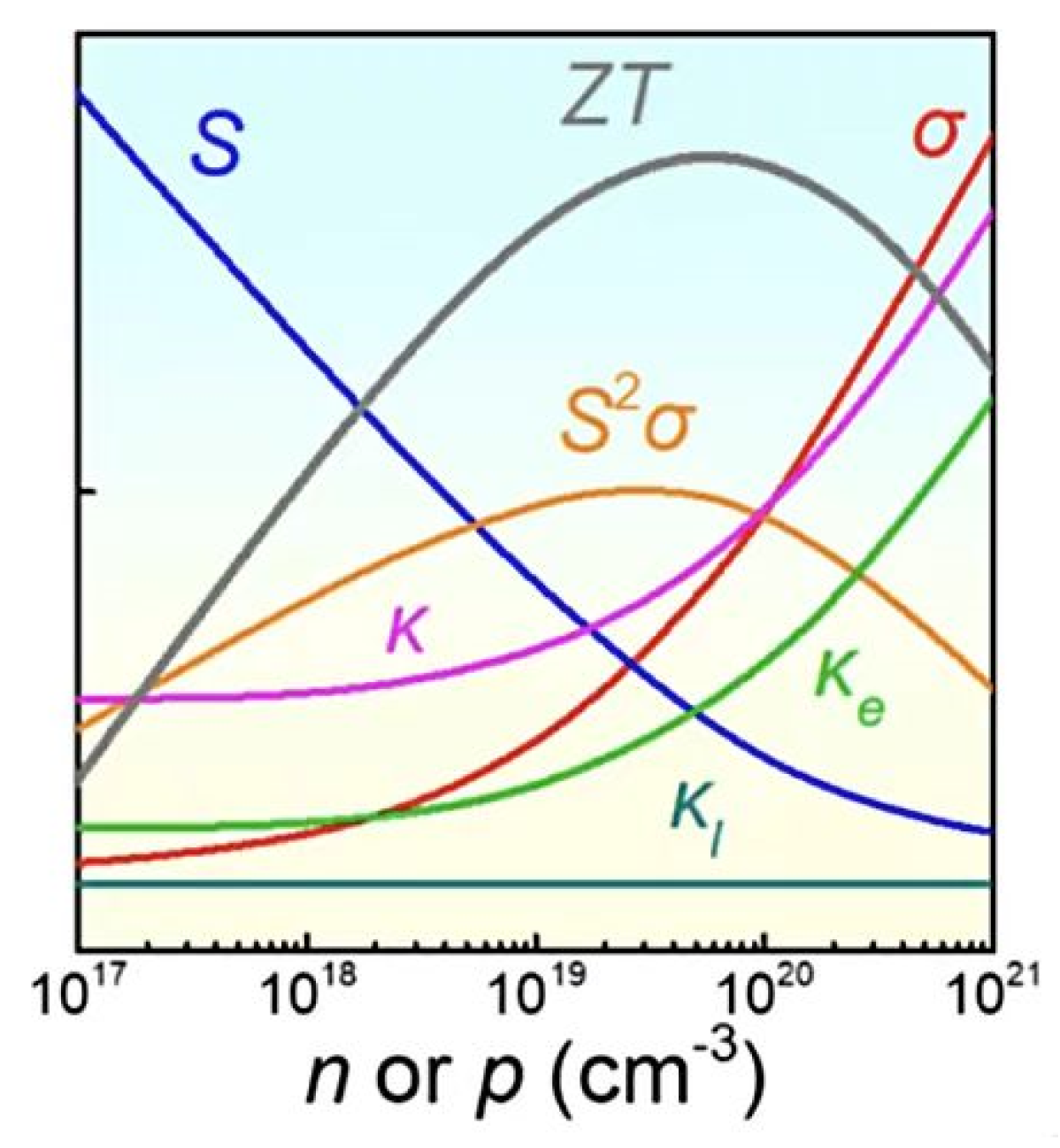
Carrier concentration control technology is one of the most critical physical mechanisms in the characteristics optimization process of doped SnSe thin films. As an intrinsic semiconductor material, SnSe’s electrical and optical characteristics are highly sensitive to carrier concentration, and the optimal carrier concentration range corresponding to different application scenarios is not the same [35]. For SnSe thin films with low intrinsic carrier concentration, introducing appropriate doping elements can effectively increase the number of carriers, causing the Fermi level to shift towards the conduction or valence band direction, thereby significantly improving the conductivity of the film and the transport efficiency of photo generated carriers. However, when the carrier concentration is too high, impurity scattering and carrier scattering effects will significantly increase, leading to a decrease in carrier mobility, which in turn weakens the further improvement of conductivity and related photoelectric or thermoelectric characteristics, as shown in Figure 5. Therefore, in doped SnSe thin films, the control of carrier concentration is not “higher, better”, but requires a reasonable balance between carrier concentration and mobility.
On the other hand, the optimal carrier concentration usually increases with temperature [36], and its theoretical relationship can be approximated as nopt~(m*T)3/2, However, conventional single element doping methods often only provide relatively constant carrier concentration over a wide temperature range, making it difficult to meet the demand for carrier concentration changes in different temperature zones. Inspired by the research on bulk thermoelectric materials [37], some scholars have proposed to dynamically control the carrier concentration with temperature changes by using multi-element synergistic doping. Although the research on this strategy in SnSe thin films is still relatively limited, it provides important ideas for regulating the carrier transport behavior of SnSe thin films in the future.
Figure 5.
Relationship between n and thermoelectric characteristics parameters [38].
Another emerging doping strategy is based on interface-assisted doping and microstructure design regulation. Although research on interface engineering in SnSe thin film systems is still in its infancy, it has been demonstrated in related solar device studies that interface layer optimization can reduce interface recombination and charge capture, thereby improving carrier extraction efficiency. This suggests that interface design has potential doping and characteristic enhancement effects in future SnSe thin film structures [39]. Interface-assisted strategies include introducing heterogeneous layers, interface modifiers, and even changing carrier scattering and band alignment through stacked structures to achieve higher electrical or optoelectronic characteristics.
In summary, the three different control techniques have varying impacts on the thin film. Firstly, band engineering control technology mainly regulates the resonance energy level and band convergence, which causes blue or red shifts in the absorption edge and affects the optical characteristics of the thin film. This makes band engineering control technology more focused on regulating the Eg of SnSe thin films, thereby affecting the absorption and photoelectric conversion efficiency of materials for different wavelengths of light. Furthermore, defect control technology dominates the regulation of lattice defects. The thermal conductivity is mainly affected by point defects, dislocation defects, and the design of multi-scale defect structures. Finally, carrier concentration control technology dominates the regulation of carrier quantity, mainly affecting the conductivity and Seebeck coefficient. By adjusting the carrier concentration, the conductivity and photosensitivity of the thin film can be mainly improved.
3.1.4. The Interaction Between Doping Mechanism and Natural Defects
In SnSe thin films, the introduction of dopants is mainly achieved through two methods: displacement doping and gap filling doping. Permutation doping refers to the substitution of Sn or Se atoms in the lattice by doping atoms. For example, Bi3+ and other metal doping elements can replace Sn2+ sites to regulate carrier concentration, while S, Te, and other doping elements tend to occupy Se sites for band engineering. This different occupancy behavior depends on the ionic radius, electronegativity, and growth kinetics of the dopant [40]. On the other hand, gap filling doping refers to the entry of small radius dopant elements into lattice gaps or interlayer gaps, which affect carrier mobility by introducing local strain and phonon scattering [41]. For example, Na+ filling can provide additional holes, but high concentrations can cause lattice distortion.
In addition to dopant doping, natural defects also play an important role in the SnSe system. The natural defects in SnSe mainly include Sn vacancies and Se vacancies. Experimental and theoretical studies generally believe that Sn vacancies are the most easily formed intrinsic point defects, with low formation energy, and dominate p-type conductivity behavior as acceptor defects [42]; Se vacancies tend to form shallow donor states, which may cause n-type conductivity [7], thereby affecting electrical compensation and carrier concentration.
- (1)
- The interaction between dopants and natural defects
There is an interaction between intrinsic defects and dopants, mainly manifested in charge compensation effects and defect recombination and passivation. In the charge replenishment effect, for example, in Ag doped SnSe thin films, when the acceptor doped AgSn coexists with the donor defect Se vacancies, a composite defect center is formed, leading to saturation or even a decrease in carrier concentration [43]; in Bi doped SnSe thin films, Bi3+ introduces an electron compensation effect when replacing Sn2+, thereby neutralizing some Sn vacancies. However, research has found that introducing excessive or mismatched doping may also lead to the formation of new defect complexes or secondary phases, increasing carrier scattering and reducing electrical characteristics.
In defect matching, dopants may suppress deep level defects by binding with vacancies. For example, In doping can combine with Sn vacancies, reduce non-radiative recombination centers, and improve photoelectric conversion efficiency [44]. Changes in doping elements and lattice composition can also be observed in Ag doped SnSe thin films [45]. Therefore, the incorporation of different doping elements and the effect of natural defects are also key factors determining the occupancy of doping elements in the lattice and the stability of the thin films.
- (2)
- The influence of growth conditions on dopant activation
On the other hand, growth conditions have a decisive impact on dopant activation and defect compensation effects. The growth parameters such as deposition temperature, deposition rate, and substrate selection not only affect the diffusion kinetics of dopants and their occupancy stability in the lattice, but also significantly regulate the probability of intrinsic defect formation.
For example, in the study of controlling the concentration of Se vacancies, adjusting the sputtering time can directly change the density of Se vacancies, thereby affecting the thermoelectric characteristics and carrier dynamics; in addition, high-temperature annealing can also promote the diffusion and displacement of dopants. However, researchers need to explore the effects of different annealing temperatures to prevent exacerbating phase separation. Horide et al. found that after annealing Bi doped SnSe thin films at 400 °C, the substitution doping of Bi increased from 60% to 85%, and the carrier concentration significantly increased. However, there is also the precipitation of second phase Bi2Se3 [46,47].
In summary, the doping behavior of SnSe thin films is a multifactorial regulatory process, and researchers need to have a deeper understanding of the interaction mechanisms between doping, defects, and growth conditions. Only through precise regulation and optimization can efficient and stable SnSe thin films be achieved, promoting their widespread application in the fields of optoelectronics and thermoelectrics.
3.2. Effect of Different Preparation Methods on Doping Behavior
As shown in Table 1, there are significant differences in the film formation mechanism, doping controllability, and application applicability among different thin film preparation methods. The thermal evaporation method is prone to “large component deviation and uneven doping”, resulting in numerous grain boundary defects, which may accelerate oxidative degradation in humid and hot environments. At the same time, “significant deviation in the doping composition of the thin film” can also lead to significant fluctuations in the film characteristics between batches during the preparation process, posing great challenges in terms of reproducibility. However, the cost of the thermal evaporation method is low and the equipment is simple. Although the uniformity of the film is slightly poor during the preparation process, it can be slightly improved through multi-source co-evaporation, and it is mostly used for the large-scale preparation of flexible devices. PLD relies on high-energy plasma plumes and has good element retention ability and high doping uniformity. The thin films prepared by PLD have low defect density and are not easily degraded under high temperatures or light, making them suitable for high stability applications such as thermoelectric modules. Meanwhile, although PLD has a small deposition area, it has good element retention and is suitable for laboratory level high-precision repetitive preparation. It is precisely because the “limited area for thin film preparation” of PLD restricts its large-scale application that it is suitable for the small-scale production of special devices and for exploring new materials and researching small area functional films. Electrochemical deposition has certain advantages in specific applications due to its low temperature, low cost, and good compatibility with flexible substrates. However, its preparation of thin films generally suffers from problems such as low crystallinity and numerous structural defects. During long-term use, characteristics deteriorate significantly. At the same time, the “low crystallinity of thin film” can also lead to different preparation batches, resulting in large fluctuations in the characteristics of the film, which poses great challenges in reproducibility and restricts its large-scale application, making it only suitable for small batch special devices.
Table 1.
Advantages and disadvantages of different preparations.
In contrast, magnetron sputtering is the preferred preparation method because magnetron sputtering exhibits more prominent comprehensive advantages in the preparation of doped SnSe thin films. This method has a high film formation rate and good process stability. It can achieve precise control of the doping ratio through target material composition design or co-sputtering, significantly improving the repeatability and consistency of the doping concentration. Thin films prepared by magnetron sputtering have fewer internal defects, effectively suppressing phase separation and oxidation, and improving the thermal and environmental stability. For example, Ag doped SnSe thin films prepared by magnetron sputtering exhibit good interfacial bonding and long-term electrical stability. Meanwhile, magnetron sputtering achieves a “uniform doping composition” and optimal repeatability through precise control of the target material composition design and process parameters. For example, In doped SnSe thin films exhibit high consistency in electrical characteristics through sputtering. It provides a reliable basis for the systematic study of the influence of doping on the optical characteristics of SnSe thin films. Taking into account the controllability of doping, uniformity of film formation, process stability, and potential for large-area preparation, magnetron sputtering is considered one of the most advantageous and practical application routes for preparing high-quality doped SnSe thin films.
3.3. The Influence of Thin Film Structural Parameters on Doping
In the preparation and characteristic optimization of SnSe thin films, the thickness, grain size, crystal orientation, and substrate selection are key structural parameters that profoundly affect the doping behavior of dopants, intrinsic defect distribution, and carrier transport characteristics.
- (1)
- The influence of film thickness
The thickness of the film directly determines the diffusion path length and stress distribution of doped elements, thereby affecting doping uniformity and activation efficiency. The report points out that thin films with low thickness tend to accumulate doping elements near the surface, forming concentration gradients; thin films with high thickness (>500 nm) are beneficial for uniform doping of the bulk phase, resulting in an increase in the grain size of the thin film, thereby improving the crystal quality and carrier mobility, and significantly improving the electrical characteristics [51]. However, if the thin film is too thick, cracks or peeling may occur due to stress accumulation. This indicates that the thickness of the thin film not only determines the macroscopic structure of the thin film, but also affects the grain boundary density and defect density, thereby affecting the carrier scattering and transport efficiency.
- (2)
- The regulatory effect of grain size
The grain size plays a significant role in the transport of charge carriers. The grain size and orientation directly affect the grain boundary segregation behavior of dopants and the directional transport of charge carriers. During the growth process of thin films, larger grains mean fewer scattering centers at grain boundaries, which helps to improve carrier mobility and reduce the aggregation or non-uniform distribution of dopants at the grain boundaries. Similar mechanisms have been reported in other semiconductor thin films, where the migration of grain boundaries and grain enlargement significantly reduce carrier scattering and increase conductivity [52,53]. Therefore, optimizing the growth conditions in SnSe thin films to promote grain growth is not only beneficial for reducing grain boundary defect density, but also for enabling dopants to more effectively occupy lattice positions and improve activation efficiency.
- (3)
- The influence of substrate selection
The substrate regulates the strain state and defect formation of thin films through lattice matching, thermal expansion coefficient, and interfacial chemical bonding. Although systematic research on the specific substrate effects of SnSe thin films is relatively limited, previous studies have shown that substrate temperature has a significant impact on the crystallinity and grain size of SnSe thin films. For example, in magnetron sputtering preparation, as the substrate temperature increases, the columnar grain size of the thin film increases and the crystal quality significantly improves, which is beneficial for optimizing the electrical and thermoelectric characteristics. The lattice mismatch of the substrate, differences in thermal expansion coefficients, and interfacial chemical reactions can all alter the strain distribution of the thin film, thereby affecting the diffusion behavior of dopants and the intrinsic defect formation energy. This means that by selecting substrate materials reasonably and controlling growth parameters, the effective activation and carrier transport mechanisms of dopants can be upregulated to a certain extent.
In summary, the microstructure parameters such as thickness, grain size, and substrate conditions of SnSe thin films can affect the crystallization behavior, defect distribution, and interface states of the thin films, deeply regulating the doping efficiency and carrier transport characteristics of dopants. Therefore, when designing doping engineering, it is necessary to take into account these thin film structural factors and combine doping strategies and growth process optimization in order to achieve the application of high-characteristic SnSe thin films in the fields of optoelectronics and thermoelectrics.
4. Effect of Doping Mechanism on Characteristics of Doped SnSe Thin Films
4.1. Effect of Band Engineering Control Technology on Doped SnSe Thin Films
In the research field of band engineering control technology of doped SnSe thin films, many teams have explored the dimensions of photovoltaic, thermoelectric, and photoelectric detection around different doped elements and preparation processes, systematically revealing the optimization mechanism of Eg regulation on the characteristics of SnSe thin films, providing key support for its cross-domain applications. The Ahmed G S team [54] used thermal evaporation technology to prepare S doped SnSe nanocrystalline films on glass substrates in 2020. With the help of band engineering control technology to enhance the photovoltaic potential, it not only widened Eg from 1.5 eV to 1.68 eB, but also improved the absorption coefficient, making α ≥ 104 cm−1, laying a solid theoretical and experimental foundation for the design of efficient SnSe-based solar cells. Subsequently, Pang J et al. [55] prepared Bi doped SnSe thin films on Si substrates by CVD in 2021, realizing the transformation of “p-type → n-type” conductivity. Research shows that Bi doping moves the Fermi level up into the conduction band, increases the density of states (DOS) near the conduction band, and then enhances the Seebeck coefficient. In the same year, the Prokeš L team [56] used PLD to prepare As doped SnSe thin films on silicon/glass substrates. At the same time, As doping also slightly increases Eg from 0.90 to 0.96 eV, opening up new possibilities for its application in phase change storage and thermoelectric fields. In 2024, Liang Zhiping’s team [57] prepared Ga doped SnSe thin films by the hydrothermal method at 180 °C. Ga replaces Sn sites to introduce a defect band “across the Fermi level”, which endows the material with metal characteristics to reduce the electronic excitation energy and significantly enhance the optical absorption coefficient, providing direct theoretical and technical support for the research and development of SnSe-based photoelectric detection devices. By 2025, the Nerella M team [58] will prepare Fe doped SnSe thin films at 150 °C by a low-temperature hydrothermal method, and further explore the regulation of the electronic structure of Fe substitutional doping Sn sites. When x = 0.01–0.05, the Eg decreases, when x = 0.10, the Eg increases slightly due to the increase in crystallinity, and when x = 0.20, it decreases again. After doping, the absorption edge is red shifted, which significantly enhances the absorption in the visible light region, providing a new idea for accurately regulating the optical response of SnSe. Therefore, these studies comprehensively show that the band engineering control technology can energize the characteristics of doped SnSe thin films in energy conversion, information storage, photoelectric detection, and other scenarios, and provide multiple paths and theoretical reference for the multi-scenario application development of the material.
In summary, the effective control of the band structure of SnSe thin films through band engineering control technology directly determines the movement of their light absorption boundaries (blue shift or red shift) and the excitation efficiency of charge carriers, thereby establishing a fundamental connection with the photoelectric conversion characteristics of the device.
4.2. Effect of Defect Control Technology on Doped SnSe Thin Films
In the research of SnSe thin films, the regulation of defect control technology has always been the core line to optimize their characteristics. Different research teams have built defect energy levels from the multi-dimensional aspects of point defect formation, lattice distortion, second phase introduction, and grain boundary engineering through the doping of a variety of elements, combined with thermal evaporation, magnetron sputtering, PLD, CVD, and other preparation processes, and achieved the characteristics breakthroughs and cross-scene applications of SnSe thin films in photovoltaic, thermoelectric, and flexible electronics and other fields.
In early studies, Ju H et al. [59] formed SnSe0.8S0.2 by doping with S in 2018. The point defects introduced by S doping significantly enhance the phonon scattering and carrier transport, and reduce the thermal conductivity. The high power factor of 297 μWcm−1K−2 is achieved at 400 K, which provides an early example for the characteristics optimization of SnSe-based thermoelectric thin films. Subsequently, Pallavolu M R et al. [44] successfully prepared In doped SnSe films on 440 °C glass substrates by a two-step method (sputtering + selenide) in 2020. Researchers found that the substitutional doping of In3+ for Sn2+ led to the reduction in the lattice constant, the improvement of crystal quality, the densification of particles, and the reduction in defects, which significantly affected the characteristics of the thin films. The XRD peak moves to a higher angle in doping, for example, the (111) peak moves from 30.46° to 30.50°+. At the same time, because the radius of the In3+ ion is less than Sn2+, the lattice shrinks. The Raman peak also moves to a higher wavenumber. The main mode shifted from 71 cm−1 to 76–77 cm−1, confirming the increase in lattice strain and defects. At the same time, In doping increases the Eg from 1.06 eV to 1.50 eV. These changes make In SnSe thin films more suitable for the photovoltaic absorption layer. The synergistic effect of the lattice strain and defect energy level optimizes the optical absorption characteristics of SnSe, making it more suitable for the photovoltaic absorption layer. In the same period, Guipeng, Li et al. [45] prepared Ag doped SnSe thin films on Si substrates at 300 °C by magnetron sputtering. Research shows that under the optimal doping amount of 7.97 at.%, XRD shows that Ag doping causes the shift in the diffraction peak of the Se phase, indicating that the introduction of the second phase causes the lattice contraction and reduces the crystal plane spacing. The change in defect energy level can increase the power factor by 52% compared with the undoped sample and achieve the power factor of 0.93 μWcm−1K−2 at 280 °C, showing the complexity of the interaction between the doped elements and lattice.
In 2020, Jalalian-Larki, B et al. [60] prepared In doped SnSe nano films on FTO substrates by electrochemical deposition at 60 °C. The researchers found that the lattice distortion introduced by In doping may be due to the occupation of interstitial sites by In ions. The Eg is reduced from undoped 1.30 eV to 1.10 eV, and the absorption in the visible region is enhanced, making the absorption edge red shift. The adjustment of the defect control technology optimizes the solar absorption, improves the efficiency of solar cells to 0.36%, and provides a new path for the efficiency improvement of SnSe-based photovoltaic devices. In 2021, Horide, T et al. [46] prepared Bi doped SnSe thin films on STO substrates at 300 °C by PLD, realizing n-type conductivity. The stacking defects introduced by Bi doping and Bi precipitation form defect energy levels and enhance thermoelectric characteristics. XRD shows that the lattice parameter a-axis length increases, indicating that Bi atoms are doped into the SnSe matrix. The power factor at 300 °C reaches 0.3 μWcm−1K−2, which opens up a direction for the research of SnSe-based n-type thermoelectric materials.
In 2022, Kumar, M et al. [61] prepared Bi doped SnSe composite films on Si/SiO2 substrates by thermal evaporation. RD and Raman analysis show that Bi doping leads to lattice distortion and phase separation of multiphase structures, which significantly enhances the thermoelectric characteristics and achieves an ultra-high power factor of 800 μWm−1K−2 at 580 K. This multiphase defect engineering not only increases the phonon scattering center (reduces the thermal conductivity) but also optimizes the conductivity through carrier transmission at the phase interface, realizing the collaborative improvement of thermoelectric characteristics. In the same year, Zhao F et al. [62] prepared Zn doped SnSe thin films on 500 °C glass substrates by the co-evaporation method. As shown in Figure 6, Zn doping changes the grain size and crystallinity. It can be seen that Zn doping causes the shift in the diffraction peak, (111) peak to high angle, and the substitutional doping of the Zn2+ ion radius for the Sn2+ ion radius causes lattice contraction, which keeps the Eg in the range of 0.86–1.1 eV, and also enhances the optical absorption ability. This coordinated regulation of lattice and defects improved the efficiency of solar cells from 0.19% to 0.55%, highlighting the potential of Zn doping in photovoltaic applications.
Figure 6.
(a) XRD images of SnSe thin film samples with different Zn doping levels. (b) Detailed XRD images of SnSe thin films with different Zn doping levels around 30.51° [62].
In 2023, Bektas, T et al. [63] prepared Sb doped SnSe thin films on soda lime glass substrates by thermal evaporation and optimized their characteristics by annealing. Sb doping mainly affects the changes in grain size and dislocation density, thus enhancing the optical absorption (α ~104 cm−1) and electrical characteristics. XRD analysis shows that the crystallization quality is improved after annealing, and the crystallization is the best at 300 °C, and the grain size is 35.74 nm. Raman spectrum reveals the vibration mode, indicating that Sb doping introduces structural changes. These findings indicate that Sb doped SnSe thin films are suitable for solar cell applications. In the same year, Horide, T. et al. [47] prepared Bi doped SnSe thin films on STO substrates at 200–300 °C by PLD. The n-type conductivity was successfully realized and used to construct π-type thermoelectric modules (p-type and n-type SnSe combination). Doping Bi mainly affects defect engineering and lattice parameters, so as to optimize the thermoelectric characteristics. The module achieves 0.09 μW output power and 0.11 V open circuit voltage at the 255 °C hot end and 155 °C cold end. This study highlights the regulatory effect of Bi doping on the thermoelectric characteristics of SnSe, which provides a basis for the development of π-type thin film modules, but the optical characteristics need to be studied in the future. Then, Sarkar P et al. [64] prepared S doped SnSe alloy films on glass substrates by mechanochemical synthesis and thermal evaporation. Researchers have found that XRD shows that all thin films are orthorhombic, and the main orientation is the (111) plane. After s doping, the (111) peak moves from 30.50° to 31.02°, indicating that the lattice shrinkage is due to the smaller radius of the S atom than that of the Se atom. It shows that the introduction of S increases the grain boundaries and defects. Therefore, S doping significantly optimizes the characteristics of the thin films, and the Eg is reduced from 1.63 eV to 1.42 eV. In addition, the Sn–S bond introduced by S doping forms the defect energy level, modifies the energy band structure, and reduces the impurity phase and lattice defects, thus enhancing the visible light absorption, making it more suitable for the photovoltaic absorption layer. In the same year, Xue, Y et al. [65] prepared α-axis oriented SnSe thin films on MgO substrates at 300 °C by PLD. Self-hole doping was achieved after selenidation at 275 °C. After selenidation, the second phase is introduced to form the defect energy level, which increases the grain boundary and point defects, enhances the phonon scattering, reduces the thermal conductivity, and finally improves the thermoelectric characteristics. In addition, more importantly, the Eg of SnSe thin films is 0.73 eV. After the post-selenidation treatment, the Eg is reduced to 0.52 eV.
In 2024, Hu, Bing et al. [66] focused on Ag doped SnSe thin films to improve the characteristics of flexible optoelectronic synaptic devices. Researchers prepared Ag doped SnSe thin films on PET substrates at room temperature by magnetron sputtering. The key indicators of the optical characteristics of the doped thin films include the Eg of 0.92 eV and the inherent high optical absorption coefficient of SnSe material, which is about 105 cm−1. Researchers have found that Ag doping mainly affects the film through defect control technology and lattice modulation. XRD and Raman spectra show that doping causes high angle shift in SnSe (400) peak and red mode, indicating that lattice distortion and crystal spacing increase, which modulates the defect state, optimizes the energy band structure, enhances carrier behavior, and realizes electrical and optical synaptic functions. Therefore, researchers believe that Ag doping can effectively solve the challenge of insufficient electrical characteristics of intrinsic SnSe, and promote the development of a flexible artificial vision system through lattice and defect control technology. In the same year, Sarkar, Prosenjit [67] deposited Te doped SnSe films on glass substrates at room temperature by thermal evaporation technology. Te, as a covalent element, replaces the Se site, modifies the energy band structure, and introduces the defect energy level, resulting in a change in the Eg. The doping of Te reduces the anti-site defects, optimizes the Eg, and reduces the undoped 1.89 eV to 1.75 eV. At the same time, with the increase in Te doping, the transmission spectrum first decreases and then increases, while the absorption coefficient is more than 104 cm−1, which makes it suitable for high-efficiency thin-film solar cells.
In 2025, Liu, Zihui et al. [68] regulated the characteristics of SnSe thin films by light induced doping. The thin films were prepared by PLD at the substrate temperature of 200 °C, showing excellent optical characteristics. Photo induced doping mainly uses Se vacancy occupied by oxygen to form defect energy levels, thus changing the conductivity. This mechanism realizes the fully optically controlled artificial synapse device to simulate biological behaviors such as visual cognition and neural network recognition. Researchers have found that the indirect Eg is about 0.90 eV and have found the wavelength selective bidirectional optical response. The negative photoconductive effect caused by photo induced oxygen desorption is highlighted. This defect control technology provides a new idea for the development of SnSe-based flexible electronic devices through the control of light induced defects. In the same year, Yin H et al. [69] successfully prepared pure SnSe and Na and Cu doped SnSe thin films on SrTiO3 substrates by PLD at the deposition temperature of 723 K in 2025. Researchers have found that the doping of Na and Cu causes lattice expansion, which makes the XRD peak shift negatively, indicating that doping induces lattice strain through point defect control technology, so as to optimize the electrical transmission characteristics. In terms of optical characteristics, UV Vis absorption spectra showed that the direct Eg of the film was adjustable in the range of 1.24 eV to 1.37 eV, and the absorption edge was located at about 1000 nm. Therefore, the doping of Na and Cu can effectively improve the carrier transport and lattice control ability of SnSe thin films through PLD, which provides the basis for integrated optothermoelectric applications.
To sum up, the defect control technology of doped SnSe thin films optimizes the key characteristics such as carrier concentration and mobility, phonon scattering, and light absorption characteristics through multi-dimensional mechanisms such as point defect formation, lattice distortion, second phase introduction, and grain boundary engineering, which provides a rich theoretical and experimental basis for its applications in photovoltaic, thermoelectric, and flexible electronics and other fields. Future research can further focus on the precise regulation of defect control technology, such as optimizing the type and concentration of defects through doping concentration and preparation processes, so as to promote the characteristics of doped SnSe thin films to a higher level.
4.3. Effect of Carrier Concentration Control Technology on Doped SnSe Thin Films
In the research of doped SnSe thin films, the accurate control of carrier concentration is one of the doping process paths to optimize its electrical and optical characteristics. Different research teams adjust the carrier concentration from multiple dimensions, such as substitutional doping and heterojunction formation through the doping of a variety of elements, combined with CVD, thermal evaporation, magnetron sputtering, electrochemical deposition, and other processes, to achieve the directional improvement of the characteristics of SnSe thin films, which has laid a key foundation for its applications in thermoelectric, photovoltaic, and flexible electronics and other fields.
In the early research, Liu S et al. [40] successfully prepared Ag doped SnSe thin films with nanostructures on mica and SiO2/Si substrates by CVD at 650 °C in 2018. An appropriate amount of Ag doping significantly improves the hole carrier concentration. Researchers have found that 1% Ag doping successfully adjusts the hole carrier concentration to a more optimized range (~1019 cm−3), and significantly improves the hole mobility and conductivity. Finally, at room temperature, the thermoelectric power factor of the 1% Ag doped sample is an order of magnitude higher than that of the undoped sample, reaching about 0.66 μWcm−1K−2, showing the great potential of Ag doping in optimizing the electrical transmission characteristics and thermoelectric applications of SnSe thin films.
In 2019, Ahmed GS et al. [70] prepared Cu doped SnSe nanocrystalline thin films on glass substrates by thermal evaporation technology, and carried out thermal diffusion doping at 400 K. Researchers have found that the carrier concentration increases from 7.983 × 1013 cm−3 undoped to 5.1 × 1014 cm−3 at 5% Cu, indicating that Cu doping provides additional holes, increases the carrier concentration, reduces the Eg from 1.5 eV to 1.3 eV, improves the absorption coefficient, and makes the absorption coefficient ≥ 104 cm−1. These changes make Cu doped SnSe thin films more suitable for photovoltaic applications, which confirms the important role of Cu doping in optimizing the characteristics of SnSe thin films. This study also provides a comprehensive characterization of Cu doped SnSe thin films, highlighting the synergistic effects of doping in band engineering control technology, defect control technology, and carrier concentration control technology and provides a basis for the design of efficient optoelectronic devices. In the same year, Chen, Z.J. et al. [71] prepared Mo doped SnSe thin films on 523 K glass substrate by multi-step magnetron sputtering. After annealing at 623 K, the MoSe2/SnSe heterojunction was formed. The results show that Mo doping mainly affects the carrier concentration, which is due to the reduction in Se vacancy, so as to optimize the thermoelectric characteristics. Therefore, Mo doping reduced the carrier concentration from 6.4 × 1018 cm−3 to 1.3 × 1018 cm−3. Then, HEO, S.H. et al. [43] prepared SnSe thin films on glass substrates at 400 °C by the solution method. As shown in Figure 7, hole doping is achieved by controlling the Se content, and the hole concentration decreases with time. The balance between conductivity and the Seebeck coefficient is optimized to obtain high texture and excellent thermoelectric characteristics, making the thermoelectric power factor reach 4.27 μWcm−1K−2 at 550 K.
Figure 7.
Relationship between electrical conductivity and temperature of SnSe thin films annealed at different temperatures [43].
In 2020, Liu, S. et al. [72] prepared Co doped SnSe thin films on Al2O3 substrates at 100–500 °C by thermal evaporation. Researchers have found that doping mainly improves the conductivity by increasing the carrier concentration. As a p-type dopant, Co increases the carrier concentration when undoped from 1016 cm−3 to 1017–1018 cm−3 to enhance the conductivity. So as to optimize and improve the thermoelectric power factor, co-doping SnSe thin films increased the power factor of 32.32 μWcm−1K−2.
In 2021, Ibraheem, S.H. [73] prepared Sb doped SnSe thin films on 503 K glass substrates by flash evaporation technology. After doping, the conductivity first increased and then decreased (increased at 1.5% and 2.5% Sb, and decreased at 3.5%), indicating that Sb doping can adjust the carrier concentration. Researchers have shown that it can be attributed to the substitutional doping of Sn or Se sites by Sb atoms, the introduction of additional carriers, and the optimization of the conductivity and photoconductivity responses.
In 2022, Ikhioya, Imosobomeh L. et al. [74] prepared Mo doped SnSe thin films on FTO substrates at room temperature by electrochemical deposition. Researchers have found that the conductivity increased from 1.663 × 10⁻¹ s/m to 1.851 × 10⁻¹ s/m, indicating that Mo doping provides additional carriers and optimizes the conductivity. At the same time, Mo doping significantly optimized the thin film characteristics, increased the Eg from 1.50 eV to 2.22 eV, and reduced the transmittance from 96% to 76%, but enhanced the optical absorption. The experiment also confirmed that Mo doping is an effective strategy to enhance the photovoltaic potential of SnSe thin films, which is suitable for optoelectronic devices. In the same year, Udofia, K.I. et al. [75] prepared Zr doped SnSe thin films on FTO substrates by electrochemical deposition, and systematically analyzed the effect of Zr doping on the characteristics of the thin films. After doping, the conductivity decreases from 3.90 × 10⁻⁶ (Ω·m)−1 to 2.17 × 10⁻⁶ (Ω·m)−1, and the resistivity increases, indicating that Zr doping may introduce scattering centers and reduce carrier mobility. The Eg increases from 1.0 eV to 1.81 eV, and the transmission edge shifts blue. These changes make Zr doped SnSe thin films suitable for photovoltaic applications. Then, HEO, S.H. et al. [76] prepared Ag doped SnSe thin films on the 673 K Si/SiO2 substrate by the solution method. Researchers have replaced the Sn site with Ag, which significantly increases the hole concentration, increases the carrier concentration from 3.48 × 1018 cm−3 to 1.30 × 1019 cm−3, optimizes the conductivity, highlights the potential of Ag carrier concentration control technology doping in low-temperature energy collection, and realizes high-characteristics thermoelectric applications, with a ZT value of about 0.93.
In 2024, Yamaguchi K et al. [77] successfully prepared high-characteristics SnSe thermoelectric thin films on a SrTiO3 single crystal substrate at 300 °C using PLD through the substitutional doping of equivalent element Te for Se site. Carrier concentration control technology doping makes the substitutional doping of Te significantly increase the hole carrier concentration, which increases the carrier concentration from 1017 cm−3 to 1018 cm−3. Its core role is to break through the thermodynamic solubility limit of Te in SnSe through the non-equilibrium growth process, and form a nanocomposite structure with orthogonal and cubic phases. This unique structure and the point defects induced by Te doping together lead to a significant increase in the hole carrier concentration, which significantly improves the conductivity and the thermoelectric power factor in the low temperature region.
In conclusion, the carrier concentration control technology, as a core parameter connecting micro doping behavior with macroscopic electrical characteristics such as conductivity and the Seebeck coefficient, is crucial for achieving high-characteristic SnSe thermoelectric thin films. Future research can further focus on the precise control of carrier concentration control technology, combined with heterostructure construction and other strategies, to promote the characteristics of SnSe thin films in thermoelectric conversion, solar cells, and other fields.
5. Comprehensive Comparison of Different Doped Elements in Doped SnSe Thin Films
5.1. Research Progress on Optical Characteristics of Doped SnSe Thin Films with Different Doping Elements
As shown in Table 2, the doping strategy provides a more flexible and efficient control means for the improvement of the optical characteristics of SnSe thin films, which can meet the needs of multi-scene optoelectronic devices from near-infrared to visible bands. While adjusting the Eg, most doped systems still maintain a high absorption coefficient, and even can enhance the optical absorption characteristics in some systems. Doped SnSe thin films have more outstanding advantages in optical characteristics and preparation flexibility than undoped SnSe thin films, and have higher research and application potential. In addition, the stability of thin film applications is excellent, which means that the characteristics of the film deteriorate less under long-term exposure to light, heat, or the environment, making it suitable for high stability scenarios. The stability of thin film applications is moderate, indicating slight characteristic degradation of the film. The stability is average and may require optimization to meet practical applications.
Table 2.
Comparison of optical characteristics of doped SnSe thin films with different elements.
5.2. Characteristics and Applications of Doping SnSe Thin Films with Different Elements
5.2.1. Application Scenarios of Doped SnSe Thin Films with Different Eg Ranges
The difference in optical characteristics of different doped SnSe thin films mainly lies in the “precise regulation” of Eg. For different ranges of Eg, they are applied in different scenarios, as shown in Table 3. In addition, the optical absorption coefficient of SnSe thin films is about 104 cm−1, and the doped SnSe thin films still maintain a high absorption advantage, which can make the thickness of the film thinner in the future. Better application in the design of the absorption layer can adapt to more flexible substrates.
Table 3.
Effects of different doping elements on optical characteristics.
As shown in Table 3, in the visible near-infrared range, the most suitable Eg for matching the solar spectrum is 1.5 eV. Therefore, doping was carried out with Pb (1.36–1.44 eV), Zn (1.44–1.51 eV), Cu (1.30–1.50 eV), S (1.42–1.63 eV), and Te (1.75–1.89 eV). The results show that the SnSe thin films are more suitable for traditional photovoltaic or visible light detection, and the SnSe thin films doped with Pb/Zn/Cu are more suitable for traditional single cells; S doped SnSe thin films are more suitable for mid-infrared detection; Te doped SnSe thin films can better optimize the optical absorption edge because of the small change in Eg broadening. The In doped SnSe thin films have a wide Eg range, which is more suitable for laminated solar cells. It can match different spectral bands by doping different concentrations of In. For In doped SnSe thin films, the Eg range is 0.90–0.96 eV, which is close to the infrared photon energy (0.9–1.2 eV), which is suitable for near-infrared photoelectric detection or expanding the lower limit of the photovoltaic spectral response. At the wide Eg level, Mo doped SnSe thin films have a wide Eg of 1.55–2.22 eV, which is close to 3.1 eV of ultraviolet photons.
Therefore, we learned from the table that there are significant differences in doping strategies between thermoelectric and optoelectronic/photovoltaic applications. The former focuses on adjusting the carrier concentration and reducing lattice thermal conductivity, while the latter focuses on optimizing light absorption, carrier separation efficiency, and interface state optimization. In thermoelectric applications, doping mainly achieves electroacoustic transport synergy through carrier concentration control technology and defect engineering control technology; in optoelectronic applications, doping is more focused on Eg adjustment and light absorption enhancement. Future researchers can further enhance the characteristics of SnSe thin films in these fields through these strategies, providing stronger theoretical and experimental support for their widespread applications.
5.2.2. Classification of Different Dopants and Predictive Frameworks
To break away from the current exploration mode of empirical trial and error in SnSe thin films doping research, we propose a rational and predictable dopant selection model to guide the design of doped SnSe thin films for different applications. This framework comprehensively considers the valence state relationship of dopants and the intrinsic relationship between element categories and characteristics, and achieves a transition from “summarizing research phenomena” to “predicting patterns”.
- (1)
- Isovalent doping
Isovalent doping refers to the doping element having the same or very close valence state to the substituted element, so as not to directly introduce significant changes in carrier types. Typical isovalent doping in SnSe thin films includes Zn2+ replacing Sn2+, Cd2+ replacing Sn2+, etc. These types of doping mainly indirectly affect the material’s characteristics through lattice distortion, local strain effects, and grain boundary structure adjustments, rather than achieving conductivity control by providing additional free carriers. The literature reports that Zn doping in SnSe thin films can significantly affect the grain size and crystal quality of the films. As the doping amount changes, the film exhibits different direct and indirect Eg while maintaining p-type conductivity behavior, indicating that the lattice effect of Zn at the same valence can optimize the characteristics of the thin films [62].
In the study of isovalent doping, Jamali-Sheini, Farid et al. [78] and others prepared Pb and Zn doped SnSe thin films on FTO substrates by the electrochemical deposition method. At 353 K, the Eg of Pb doped SnSe thin films is in the range of 1.36–1.44 eV, and that of Zn doped SnSe thin films is in the range of 1.44–1.51 eV. Ahmed G S et al. [70] prepared Cu doped SnSe thin films on glass substrates by the thermal evaporation method. At 400 K, the Eg of Cu doped SnSe thin films ranges from 1.30 eV to 1.50 eV, and the absorption coefficients of all doped SnSe thin films are greater than or equal to 104 cm−1. Pallavolu M R et al. [44] prepared In doped SnSe thin films on glass substrates using the sputtering + selenide technology of magnetron sputtering. At the temperature of 713 K, the Eg changes from 1.06 undoped to 1.50 eV after doping. Therefore, the Eg of In doped SnSe thin films is in the range of 1.06–1.50 eV.
From a theoretical perspective, isovalent doping does not directly change the Fermi level like aliovalent doping, so its impact on band structure is often subtle. According to first principles calculations, the electronic structure and optical characteristics of single-layer SnSe doped with transition metals such as Zn, Sc, V, etc., will be adjusted due to the orbital hybridization of doped atoms. For example, Sc and V doping can even transform indirect Eg into direct Eg, and the binding energy and formation energy of different doping systems also indicate that doping atoms can stably embed into the SnSe lattice and have an impact on electron transport channels [79].
However, a significant challenge of isovalent doping is its limited impact on carrier concentration. Due to the fact that this doping does not actively provide charge carriers, its effect is often less significant than that of aliovalent doping in applications that require a significant increase in charge carrier concentration, such as high conductivity or high power factor. In addition, the lattice distortion effect of isovalent doping may exhibit different effects under different preparation conditions, which puts higher demands on the repeatability of the thin films. Therefore, the isovalent doping mainly affects the lattice and structural quality, rather than directly changing the carrier concentration.
- (2)
- Aliovalent doping
Unlike isovalent doping, aliovalent doping is one of the most common and effective control methods in the study of SnSe thin films. Aliovalent doping refers to the doping of atoms with different valence states from the replaced atoms, which directly changes the carrier concentration and carrier type of the material. For example, when Ag+, Cu2+, and Bi3+ replace Sn2+, additional holes or electrons are introduced, effectively increasing the carrier concentration and changing the Fermi level position. When studying the thermoelectric characteristics of SnSe, Bi doping has been shown to significantly enhance the Seebeck coefficient and carrier concentration. For example, Bi doped SnSe thin films exhibit significantly higher Seebeck coefficients than undoped films, which is mainly attributed to the Fermi level shift caused by doping and the increase in charge carriers, thereby changing the electroacoustic transport behavior and significantly optimizing the thermoelectric characteristics [55].
In the study of aliovalent doping, Prokeš L et al. [56] prepared As doped SnSe thin films on glass substrates by PLD. At 633 K, the Eg of As doped SnSe thin films is in the range of 0.90–0.96 eV. Hu B et al. [66] prepared Ag doped SnSe thin films on PET substrates by magnetron sputtering. The Eg of Ag doped SnSe thin films is 0.92 eV. Ikhioya, Imosobomeh L et al. [74] prepared Mo doped SnSe thin films on FTO substrates by electrochemical deposition. At 300 K, the absorbance of Mo doped SnSe thin films increases, and the Eg range is 1.55–2.22 eV.
Aliovalent doping is not only important in the field of thermoelectric materials, but is also crucial in optoelectronic applications. Taking Ag or Cu doping as an example, according to existing review reports, for SnSe and similar IV–VI compound doping systems, the carrier concentration can be increased to the order of ~1019 cm−3 through aliovalent doping. This growth is crucial for achieving high conductivity and thermoelectric power factors, but it is also accompanied by a decrease in mobility and the possibility of second phase precipitation caused by excessive doping. When the dopant exceeds its solubility limit, the precipitated secondary phase such as AgSnSe2 will reduce the carrier effectiveness and cause carrier scattering, resulting in a decrease in carrier mobility, leading to saturation or even a downward trend in the improvement of transport characteristics [80].
When designing aliovalent doping systems, it is not only necessary to estimate the contribution of dopants to the carrier concentration, but also to consider the structural and scattering effects they may cause in actual thin films. These mechanisms help explain why different reports in the literature observe different trends in the electronic characteristics under similar doping systems, and provide ideas for designing high-characteristic doped SnSe thin films.
- (3)
- Chalcogen doping
Chalcogen doping refers to the introduction of elements from the same group, such as S or Te, into the SnSe lattice to replace Se sites. This type of doping mainly achieves band engineering by changing the orbital hybridization of the valence and conduction bands, rather than simply adjusting the characteristics by changing the carrier concentration. The atomic radius and chemical bond characteristic of chalcogenides and Se are similar, allowing them to exist stably in the SnSe lattice and significantly affecting the band structure of the material.
In the study of chalcogen doping, Ahmed G S et al. [54] prepared S doped SnSe thin films on glass/Si substrates by thermal evaporation. At 300 K, Eg increases with the increase in S concentration, and the Eg of S doped SnSe thin films is in the range of 1.50–1.68 eV. Sarkar, P et al. [64] prepared S doped SnSe thin films on glass substrates by thermal evaporation. At 623 K, the Eg of S doped SnSe thin films is in the range of 1.42–1.63 eV. Sarkar, P et al. [67] prepared Te doped SnSe thin films on glass substrates by the thermal evaporation method. At 300 K, with the increase in Te concentration, the Eg increases, and the grain size decreases. The Eg of Te doped SnSe thin films is 1.75–1.89 eV, and the absorption coefficient α is 105 cm−1, which is beneficial for expanding the visible light absorption range and providing a wider response window for photovoltaic or optoelectronic applications.
Another important aspect of chalcogen doping is that it can change the band edge density and state distribution through atomic orbital hybridization, achieving finer band engineering. For example, in SnSe-based photodetectors, through sulfur diffusion technology, the thin film exhibits better crystal structure consistency under annealing conditions, significantly improving the device’s response characteristics and providing experimental evidence for further understanding the structural regulation of sulfur doping. However, chalcogen doping also poses challenges. When the sulfur group is highly doped, it may lead to lattice distortion and an increase in defect states, resulting in carrier scattering and an increase in non-radiative recombination centers. Therefore, when designing chalcogen doping schemes, it is necessary to balance the Eg regulation and carrier transport, ensuring that the required Eg adjustment is achieved without significantly sacrificing electrical characteristics [81].
In summary, we conducted a systematic analysis of the mechanisms of isovalent doping, aliovalent doping, and chalcogen doping, as shown in Table 4. For isovalent doping, doping with Zn and other isovalent metals introduces moderate lattice distortion, improves grain size, and suppresses the formation of deep level defects to enhance the crystalline quality and structural stability of the thin film. Aliovalent doping, due to the different valence states of doping atoms and Sn, can directly participate in the charge compensation process as donors or acceptors, and therefore its dominant regulatory mechanism is carrier control. This type of doping can effectively regulate the carrier concentration and is the core means to achieve conductivity enhancement and carrier type conversion. Chalcogen doping mainly affects the hybridization of valence band orbitals and band edge structures by replacing Se sites with elements such as S and Te. It achieves absorption edge regulation through band engineering control technology.
Table 4.
Application of classification different dopants.
Based on the summary of Table 4, we have established a predictive design route for the doping mechanism of SnSe thin films, as shown in Figure 8. This route elevates the existing experience-based doping research mode to a rule-based design method, which can not only systematically solve the problem of the literature divergence, but also provide theoretical guidance for the rapid screening and characteristic optimization of future new doping systems, and is of great significance for the engineering application of SnSe-based optoelectronic devices.
Figure 8.
Prediction design route for doping mechanism of SnSe thin films.
6. Correlation Mechanism Between Doping and Optical Characteristics of Doped SnSe Thin Films
6.1. Effect of Different Doping Atomic Fraction Optical Characteristics
Doping atomic fraction (at.%) is one of the core parameters to control the optical characteristics of SnSe thin films. By changing the electronic structure, carrier concentration, and defect density of the state of the material, it can realize the directional adjustment of key optical parameters such as absorption spectrum, transmittance, and Eg. A large number of experimental and theoretical studies show that low atomic fraction doping mainly optimizes the optical characteristics through band trimming, while atomic fraction doping will cause carrier scattering and non-radiative recombination, leading to the deterioration of optical characteristics. This concentration dependent optical behavior provides important parameter guidance for the application of SnSe thin films in photovoltaic and photoelectric detection and other fields.
6.1.1. Low Atomic Fraction Doping: Band Trimming and Optical Characteristics Optimization
Low atomic fraction doping usually means that the atomic percentage of doped elements is less than 3%, which is a common strategy for optimizing the optical characteristics of doped SnSe thin films. Doping within this atomic fraction range will not significantly change the crystal structure of the material, but will achieve precise control of the optical characteristics by introducing a small amount of impurity energy levels or adjusting the original energy band structure.
- (1)
- Band trimming and absorption enhancement
Low atomic fraction doping will slightly adjust the band structure of doped SnSe thin films, such as expanding the valence band or conduction band by orbital hybridization of impurity atoms, or reducing the Eg by introducing shallow impurity levels. For example, in Cu doped SnSe thin films, the low atomic fraction doping of Cu replaces Sn sites, and the Eg is slightly reduced from 1.5 eV to 1.3 eV. This Eg adjustment not only enhances the absorption in the visible region, but also makes the absorption edge move towards the short wave direction (blue shift), covering a wider range of the solar spectrum.
- (2)
- Carrier concentration optimization and defect state suppression
Low atomic fraction doping will increase the carrier concentration in the material, but will not lead to a significant enhancement of carrier scattering. For example, in Ag doped SnSe films, 0.93 at.% Ag doping increases the hole carrier concentration from 1016 cm−3 to 1017 cm−3, while the defect density of the states does not increase significantly. In addition, low atomic fraction doping can also inhibit the formation of defect states, because impurity atoms occupy some defect sites, such as Sn vacancies, reducing the number of non-radiative recombination centers. For example, in In doped SnSe thin films, 1 at.% In doping reduces the absorption edge and sharpness is significantly enhanced, indicating that the carrier absorption is more concentrated in a specific wavelength range, and the optical characteristics are better.
- (3)
- Balance between Eg and transmissivity
Low atomic fraction doping also affects the Eg and transmittance of SnSe thin films. For example, in Zn doped SnSe thin films, 0.285 at.% Zn doping keeps the Eg at 0.86–1.1 eV, which is suitable for photovoltaic applications, while the transmittance increases from 30% to 70% in the visible region. This balance of Eg and transmissivity makes SnSe thin film not only effectively absorb sunlight, but also transmit part of the light, which is suitable for the window layer or absorption layer of solar cells.
6.1.2. High Atomic Fraction Doping: Negative Effects of Carrier Scattering and Non-Radiative Recombination
- (1)
- Carrier scattering and mobility reduction
High atomic fraction doping will introduce a large number of impurity ions, which will produce Coulomb electric fields and have a strong scattering effect on carriers. For example, in Sb doped SnSe thin films, when the Sb atomic fraction increases from 1 at.% to 3.5 at.%, the carrier mobility decreases from ~100 cm2v−1s−1 to ~10 cm2v−1s−1. The decrease in mobility will lead to the decrease in absorption efficiency. In addition, high atomic fraction doping will also lead to the aggravation of lattice distortion, because the radius of impurity atoms is different from Sn or Se atoms, which easily causes the change in the lattice constant and further increases carrier scattering.
- (2)
- Non-radiative recombination and reduction in absorption coefficient
High atomic fraction doping will increase the density of the states of defects, especially deep level defects, which will become non-radiative recombination centers. For example, in Bi doped SnSe thin films, when the Bi atomic fraction exceeds 5 at.%, the density of the defect states in these phases is as high as 1020 cm−3, the probability of non-radiative recombination increases significantly, and the absorption coefficient decreases from ~104 cm−1 to ~103 cm−1. In addition, high atomic fraction doping will also lead to Eg contraction, because the Fermi level enters the conduction band or valence band, resulting in the reduction in the effective Eg and the red shift in the absorption edge, covering more infrared regions, but the absorption in the visible region will be weakened.
- (3)
- Deterioration of optical characteristics and structural defects
High atomic fraction doping can also lead to an increase in structural defects in SnSe films, such as the decrease in grain size and the increase in grain boundaries. These structural defects will scatter photons, reduce the transmittance of light, and increase the absorption loss of light. For example, in Ag doped SnSe thin films, when the Ag atomic fraction exceeds 7 at.%, the grain size of these phases decreases from ~1 µm to ~100 nm, the number of grain boundaries increases, and the transmittance in the visible region decreases from 70% to 30%. In addition, high atomic fraction doping will also lead to an increase in the surface roughness of the film and further reduce the light transmittance.
Therefore, in the doping design of SnSe thin films, the effect of atomic fraction doping on the optical characteristics of SnSe thin films has a significant atomic fraction dependence. Low atomic fraction doping optimizes the optical characteristics by fine-tuning the Eg and improves the absorption coefficient and carrier mobility; high atomic fraction doping causes carrier scattering and non-radiative recombination, leading to the deterioration of the optical characteristics. By reasonably selecting doping elements and their atomic fractions, combined with the triple mechanism of carrier concentration control, band structure optimization, and defect state control, a balance can be achieved between carrier dynamics and lattice stability, thereby achieving the directional optimization of optical characteristics. This atomic fraction doping dependent behavior not only provides theoretical guidance for the photovoltaic and optoelectronic detection applications of SnSe thin films, but also provides a general idea for the characteristics control strategies of related functional semiconductor thin film materials.
6.2. Effect of Structure Control on Optical Characteristics
In the frontier research of thin films, the correlation between the structure and optical characteristics is the core issue to guide the design and characteristics optimization of thin film materials. In particular, the crystal structure, stoichiometry, and surface morphology of the film, as the intrinsic characteristics of the film, can directly determine the change law of optical constants, such as the refractive index, absorption coefficient, and transmittance. The doping process described in this paper is explored through three main influence paths, aiming to enable researchers to improve and enhance the doping process of thin films in the future.
In the regulation of the doping process on the characteristics of thin films, the three mechanisms of band engineering control technology, defect control technology, and carrier concentration control technology are different in physical origin and action form. From the dimensions of carrier concentration, lattice defects, and microstructure, they systematically shape the core film characteristics such as light absorption, transmission, and optical Eg of thin films, providing a hierarchical theoretical framework for the design and characteristics optimization of thin films such as solar cells.
As shown in Figure 9, the band engineering control technology, as the essential characterization of the energy and spatial distributions of the electronic energy state, dominates the optical response boundary from the characteristics of electronic energy level reconstruction by modulating the position of the absorption edge (blue shift/red shift). The blue shift or red shift makes the band structure narrower/wider, which directly changes the absorption threshold of the film material for different wavelengths of light and determines its spectral response range. Therefore, the doping process has become the key to break through the traditional Eg limit and realize the wide spectral absorption of thin film materials. Secondly, the influence of the carrier concentration control technology focuses on the number of electrons and holes in the thin film material. When the carrier concentration increases, the Coulomb interaction between photons and free carriers increases, resulting in a significant decrease in transmittance. This is different from the traditional doping control methods. The control of carrier concentration can make the thin film materials focus more on external excitation, such as the dynamic real-time modulation of light interaction by light induction or the doping process.
Figure 9.
Schematic diagram of the influence of doping mechanism.
Third, defect control technology is a new framework in the Eg through the defect energy level, so that the electrons in the thin film material can complete the absorption of the sub Eg through the defect state; at the same time, non-radiative recombination takes defects as the energy dissipation center, converting the energy of the electron hole pair into heat, thus reducing the luminous efficiency. The “destruction” and “construction” effect of the defect control technology on the Eg of the thin film makes the doped thin film material able to provide guidance and application for specific optical functional materials, and may also become one of the problems of characteristics degradation in the design of optoelectronic devices, which fully reflects the duality of the defect process as a means of the doping mechanism, and also provides ideas for future researchers to regulate the characteristics of the thin films through defect control technology, and promote breakthroughs in technologies such as efficient photoelectric conversion and intelligent light regulation.
7. Conclusions
This article systematically reviews the latest research progress in the doping control technology, characteristics, and applications of doped SnSe thin films. By analyzing different doping elements and preparation processes, we found that the band engineering control technology, defect control technology, and carrier concentration control technology can effectively regulate SnSe thin films, thereby significantly improving their optical and thermoelectric characteristics. At the same time, we also found that low atomic fraction doping can enhance light absorption through band tuning, while high atomic fraction doping may lead to carrier scattering and non-radiative recombination, which in turn deteriorates characteristics. Based on the above analysis, future research should focus on the following directions:
- Doping precision and reproducibility: By optimizing the preparation process parameters, atomic level doping control can be achieved to avoid characteristics degradation caused by high atomic fraction, improving the experimental reproducibility and device consistency.
- Collaborative optimization of defect control technology and interface design: Combining first principles/defect calculation with high-throughput experiments to quickly screen potential doping elements and atomic fraction windows, and accelerating material optimization through theoretical prediction and experimental verification in a closed loop. By utilizing post annealing or interface engineering to suppress non-radiative recombination, nanocomposite phases or heterojunctions can be constructed to simultaneously reduce thermal conductivity and increase carrier concentration, thereby enhancing the characteristics of thin films.
- Industrialization challenge: To translate laboratory characteristics into actual devices, attention needs to be paid to the stability of thin films under long-term light exposure, thermal cycling, and environmental conditions (humidity/oxygen), simultaneously exploring process compatibility on low-temperature soluble/flexible substrates to advance the application of flexible optoelectronics and wearable energy harvesting devices.
In summary, doping mechanisms provide diverse and effective ways to regulate the characteristics of SnSe thin films. Through the synergistic optimization of process microstructure characteristics, combined with advanced characterization and theoretical guidance, SnSe doped thin films are expected to achieve higher characteristics and practical application conversions in areas such as efficient, broad-spectrum light detection, thin-film photovoltaics, and flexible thermoelectric devices.
Author Contributions
Conceptualization, Z.L., Z.G., and C.Z.; methodology, J.Z., F.T., and X.C.; writing—original draft preparation, Z.G. and X.L.; writing—review and editing, Y.F. and Y.X.; visualization, K.L., W.L., and C.H.; supervision, Y.Y. and Y.Q.; funding acquisition, Y.Q. All authors have read and agreed to the published version of the manuscript.
Funding
This work was supported in part by the specific research fund for the Innovation Platform for Academicians of Hainan Province under Grant YSPTZX202513; in part by the Key Research and Development Projects in Hainan Province under Grant ZDYF2025GXJS007; in part by the Hainan Normal University Graduate Students Innovative Scientific Research Project under Grant S202511658042 and Grant S202511658046; in part by the Hainan Normal University College Students’ Innovation and Entrepreneurship Open Fund (Banyan Tree Fund) Project under Grant RSXH20231165803X, Grant RSXH20231165811X, Grant RSYH20231165806X, Grant RSYH20231165824X, and Grant RSYH20231165833X; in part by the Hainan Province International Science and Technology Cooperation R&D Project under Grant GHYF2025030; and in part by the National Natural Science Foundation of China under Grant 62464006.
Institutional Review Board Statement
Not applicable.
Informed Consent Statement
Not applicable.
Data Availability Statement
Data sharing is not applicable. No new data were created or analyzed in this study.
Conflicts of Interest
The authors declare no conflicts of interest.
References
- Shi, W.; Gao, M.; Wei, J.; Gao, J.; Fan, C.; Ashalley, E.; Li, H.; Wang, Z. Tin selenide (SnSe): Growth, properties, and applications. Adv. Sci. 2018, 5, 1700602. [Google Scholar] [CrossRef] [Scilit] [PubMed]
- Reddy, V.R.M.; Gedi, S.; Pejjai, B.; Park, C. Perspectives on SnSe-based thin film solar cells: A comprehensive review. J. Mater. Sci. Mater. Electron. 2016, 27, 5491–5508. [Google Scholar] [CrossRef] [Scilit]
- Boscher, N.D.; Carmalt, C.J.; Palgrave, R.G.; Parkin, I.P. Atmospheric pressure chemical vapour deposition of SnSe and SnSe2 thin films on glass. Thin Solid Film. 2008, 516, 4750–4757. [Google Scholar] [CrossRef] [Scilit]
- Bell, L.E. Cooling, Heating, Generating Power, and Recovering Waste Heat with Thermoelectric Systems. Science 2008, 321, 1457–1461. [Google Scholar] [CrossRef] [Scilit]
- Li, F.; Wang, H.; Huang, R.; Chen, W.; Zhang, H. Recent advances in SnSe nanostructures beyond thermoelectricity. Adv. Funct. Mater. 2022, 32, 2200516. [Google Scholar] [CrossRef] [Scilit]
- Universiti Sains Malaysia. Asian Conference on X-Rays and Related Techniques in Research and Industry; Proceedings; Universiti Sains Malaysia: Gelugor, Malaysia, 1996. [Google Scholar]
- Shi, G.; Kioupakis, E. Quasiparticle band structures and thermoelectric transport properties of p-type SnSe. J. Appl. Phys. 2015, 177, 065103. [Google Scholar] [CrossRef] [Scilit]
- Zhao, L.D.; Lo, S.H.; Zhang, Y.; Sun, H.; Tan, G.; Uher, C.; Wolverton, C.; Dravid, V.P.; Kanatzidis, M.G. Ultralow thermal conductivity and high thermoelectric figure of merit in SnSe crystals. Nature 2014, 508, 373–377. [Google Scholar] [CrossRef] [Scilit]
- Jeong, G.; Kim, J.; Gunawan, O.; Pae, S.R.; Kim, S.H.; Song, J.Y.; Lee, Y.S.; Shin, B. Preparation of single-phase SnSe thin-films and modification of electrical properties via stoichiometry control for photovoltaic application. J. Alloys Compd. 2017, 722, 474–481. [Google Scholar] [CrossRef] [Scilit]
- Gao, B.; Hu, J.; Tang, S.; Xiao, X.; Chen, H.; Zuo, Z.; Qi, Q.; Peng, Z.; Wen, J.; Zou, D. Organic-Inorganic Perovskite Films and Efficient Planar Heterojunction Solar Cells by Magnetron Sputtering. Adv. Sci. 2021, 8, 2102081. [Google Scholar] [CrossRef] [Scilit]
- Heremans, J.P.; Wiendlocha, B.; Chamoire, A.M. Resonant levels in bulk thermoelectric semiconductors. Energy Environ. Sci. 2012, 5, 5510–5530. [Google Scholar] [CrossRef] [Scilit]
- Zhang, Q.Y.; Wang, H.; Liu, W.S.; Wang, H.Z.; Yu, B.; Zhang, Q.; Tian, Z.T.; Ni, G.; Lee, S.; Esfarjani, K.; et al. Enhancement of thermoelectric figure-of-merit by resonant states of aluminium doping in lead selenide. Energy Environ. Sci. 2012, 5, 5246–5251. [Google Scholar] [CrossRef] [Scilit]
- Jaworski, C.M.; Kulbachinskii, V.; Heremans, J.P. Resonant level formed by tin in Bi2Te3 and the enhancement of room-temperature thermoelectric power. Phys. Rev. B 2009, 80, 233201. [Google Scholar] [CrossRef] [Scilit]
- Hussain, T.; Li, X.; Danish, M.H.; Rehman, M.U.; Zhang, J.; Li, D.; Chen, G.; Tang, G. Realizing high thermoelectric performance in eco-friendly SnTe via synergistic resonance levels, band convergence and endotaxial nanostructuring with Cu2Te. Nano Energy 2020, 73, 104832. [Google Scholar] [CrossRef] [Scilit]
- Liu, W.; Tan, X.; Yin, K.; Liu, H.; Tang, X.; Shi, J.; Zhang, Q.; Uher, C. Convergence of Conduction Bands as a Means of Enhancing Thermoelectric Performance of n-Type Mg2Si1–xSnx Solid Solutions. Phys. Rev. Lett. 2012, 108, 166601. [Google Scholar] [CrossRef] [Scilit]
- Jood, P.; Male, J.P.; Anand, S.; Matsushita, Y.; Takagiwa, Y.; Kanatzidis, M.G.; Snyder, G.J.; Ohta, M. Na Doping in PbTe: Solubility, Band Convergence, Phase Boundary Mapping, and Thermoelectric Properties. J. Am. Chem. Soc. 2020, 142, 15464–15475. [Google Scholar] [CrossRef] [Scilit] [PubMed]
- Zhao, L.D.; Wu, H.J.; Hao, S.Q.; Wu, C.I.; Zhou, X.Y.; Biswas, K.; He, J.Q.; Hogan, T.P.; Uher, C.; Wolverton, C.; et al. All-scale hierarchical thermoelectrics: MgTe in PbTe facilitates valence band convergence and suppresses bipolar thermal transport for high performance. Energy Environ. Sci. 2013, 6, 3346–3355. [Google Scholar] [CrossRef] [Scilit]
- Chen, Z.; Jian, Z.; Li, W.; Chang, Y.; Ge, B.; Hanus, R.; Yang, J.; Chen, Y.; Huang, M.; Snyder, G.J.; et al. Lattice Dislocations Enhancing Thermoelectric PbTe in Addition to Band Convergence. Adv. Matter. 2017, 29, 1606768. [Google Scholar] [CrossRef] [Scilit]
- Wu, H.; Chang, C.; Feng, D.; Xiao, Y.; Zhang, X.; Pei, Y.; Zheng, L.; Wu, D.; Gong, S.; Chen, Y.; et al. Synergistically optimized electrical and thermal transport properties of SnTe via alloying high-solubility MnTe. Energy Environ. Sci. 2015, 8, 3298–3312. [Google Scholar] [CrossRef] [Scilit]
- Tan, G.; Zhao, L.D.; Shi, F.; Doak, J.W.; Lo, S.H.; Sun, H.; Wolverton, C.; Dravid, V.P.; Uher, C.; Kanatzidis, M.G. High Thermoelectric Performance of p-Type SnTe via a Synergistic Band Engineering and Nanostructuring Approach. J. Am. Chem. Soc. 2014, 136, 7006–7017. [Google Scholar] [CrossRef] [Scilit] [PubMed]
- Zheng, L.; Li, W.; Lin, S.; Li, J.; Chen, Z.; Pei, Y. Interstitial Defects Improving Thermoelectric SnTe in Addition to Band Convergence. ACS Energy Lett. 2017, 2, 563–568. [Google Scholar] [CrossRef] [Scilit]
- Hong, M.; Wang, Y.; Liu, W.; Matsumura, S.; Wang, H.; Zou, J.; Chen, Z.G. Arrays of Planar Vacancies in Superior Thermoelectric Ge1−x−yCdxBiyTe with Band Convergence. Adv. Energy Mater. 2018, 8, 1801837. [Google Scholar] [CrossRef] [Scilit]
- Sun, Q.; Li, M.; Shi, X.L.; Xu, S.D.; Liu, W.D.; Hong, M.; Lyu, W.; Yin, Y.; Drgusch, M.; Zou, J.; et al. Versatile Vanadium Doping Induces High Thermoelectric Performance in GeTe via Band Alignment and Structural Modulation. Adv. Energy Mater. 2021, 11, 2100544. [Google Scholar] [CrossRef] [Scilit]
- Li, M.; Sun, Q.; Xu, S.D.; Hong, M.; Lyu, W.Y.; Liu, J.X.; Wang, Y.; Dargusch, M.; Zou, J.; Chen, Z.G. Optimizing Electronic Quality Factor toward High-Performance Ge1−x−yTaxSbyTe Thermoelectrics: The Role of Transition Metal Doping. Adv. Matter. 2021, 33, 2102575. [Google Scholar] [CrossRef] [Scilit] [PubMed]
- Pei, Y.; Shi, X.; Lalonde, A.; Wang, H.; Chen, L.; Snyder, G.J. Convergence of electronic bands for high performance bulk thermoelectrics. Nature 2011, 473, 66–69. [Google Scholar] [CrossRef] [Scilit]
- Tan, G.; Zhao, L.D.; Kanatzidis, M.G. Rationally Designing High-Performance Bulk Thermoelectric Materials. Chem. Rev. 2016, 116, 12123–12149. [Google Scholar] [CrossRef] [Scilit] [PubMed]
- He, J.; Kanatzidis, M.G.; Dravid, V.P. High performance bulk thermoelectrics via a panoscopic approach. Mater. Today 2013, 16, 166–176. [Google Scholar] [CrossRef] [Scilit]
- Pei, Y.; Zheng, L.; Li, W.; Lin, S.; Chen, Z.; Wang, Y.; Xu, X.; Yu, H.; Chen, Y.; Ge, B. Interstitial Point Defect Scattering Contributing to High Thermoelectric Performance in SnTe. Adv. Electron. Mater. 2016, 2, 1600019. [Google Scholar] [CrossRef] [Scilit]
- Fu, L.; Yin, M.; Wu, D.; Li, W.; Feng, D.; Huang, L.; He, J. Large enhancement of thermoelectric properties in n-type PbTe via dual-site point defects. Energy Environ. Sci. 2017, 10, 2030–2040. [Google Scholar] [CrossRef] [Scilit]
- Kumar, V.N.; Hayakawa, Y.; Udono, H.; Inatomi, Y. An Approach to Optimize the Thermoelectric Properties of III–V Ternary InGaSb Crystals by Defect Engineering via Point Defects and Microscale Compositional Segregations. Inorg. Chem. 2019, 58, 11579–11588. [Google Scholar] [CrossRef] [Scilit]
- Qin, B.; Zhang, Y.; Wang, D.; Zhao, Q.; Gu, B.; Hu, H.; Zhang, H.; Ye, B.; Pennycook, S.J.; Zhao, L.D. Ultrahigh Average ZT Realized in p-Type SnSe Crystalline Thermoelectrics through Producing Extrinsic Vacancies. J. Am. Chem. Soc. 2020, 142, 5901–5909. [Google Scholar] [CrossRef] [Scilit]
- Chen, Z.; Ge, B.; Li, W.; Lin, S.; Shen, J.; Chang, Y.; Hanus, R.; Snyder, J.; Pei, Y. Vacancy-induced dislocations within grains for high-performance PbSe thermoelectrics. Nat. Commun. 2017, 8, 13828. [Google Scholar] [CrossRef] [Scilit] [PubMed]
- Kim, S.I.; Lee, K.H.; Mun, H.A.; Kim, H.S.; Hwang, S.W.; Roh, J.W.; Yang, D.J.; Shin, W.H.; Li, X.S.; Lee, Y.H.; et al. Dense dislocation arrays embedded in grain boundaries for high-performance bulk thermoelectrics. Science 2015, 348, 109–114. [Google Scholar] [CrossRef] [Scilit] [PubMed]
- Biswas, K.; He, J.; Blum, I.D.; Wu, C.I.; Hogan, T.P.; Seidman, D.N.; Dravid, V.P.; Kanatzidis, M.G. High-performance bulk thermoelectrics with all-scale hierarchical architectures. Nature 2012, 489, 414–418. [Google Scholar] [CrossRef] [Scilit]
- Snyder, G.J.; Toberer, E.S. Complex thermoelectric materials. Nat. Mater. 2008, 7, 105–114. [Google Scholar] [CrossRef] [Scilit]
- Mao, J.; Liu, Z.; Zhou, J.; Zhu, H.; Zhang, Q.; Chen, G.; Ren, Z. Advances in Thermoelectrics. Adv. Phys. 2018, 67, 69–147. [Google Scholar] [CrossRef] [Scilit]
- Zhang, Q.; Song, Q.; Wang, X.; Sun, J.; Zhu, Q.; Dahal, K.; Lin, X.; Cao, F.; Zhou, J.; Chen, S.; et al. Deep defect level engineering: A strategy of optimizing the carrier concentration for high thermoelectric performance. Energy Environ. Sci. 2018, 11, 933–940. [Google Scholar] [CrossRef] [Scilit]
- Shi, X.L.; Zou, J.; Chen, Z.G. Advanced Thermoelectric Design: From Materials and Structures to Devices. Chem. Rev. 2020, 120, 7399–7515. [Google Scholar] [CrossRef] [Scilit]
- Younsi, Z.; Bencherif, H.; Meddour, F.; Sasikumar, P.; Zereg, A.; Mark, V.; Perumal, R. Mitigating the interface defects influence on SnSe solar cells using optimized electron transport layer. Discov. Mater. 2024, 4, 85. [Google Scholar] [CrossRef] [Scilit]
- Liu, S.; Sun, N.; Liu, M.; Sucharitakul, S.; Gao, X.P.A. Nanostructured SnSe: Synthesis, doping, and thermoelectric properties. J. Appl. Phys. 2018, 123, 115109. [Google Scholar] [CrossRef] [Scilit]
- Zhao, L.D.; Tan, G.J.; Hao, S.Q.; He, J.Q.; Pei, Y.L.; Chi, H.; Wang, H.; Gong, S.K.; Xu, H.B.; Dravid, V.P.; et al. Ultrahigh power factor and thermoelectric performance in hole-doped single-crystal SnSe. Science 2015, 351, 141–144. [Google Scholar] [CrossRef] [Scilit]
- Yadav, M.; Singh, V.; Sharma, S.K.; Archana, J.; Navaneethan, M.; Pathak, A.; Bharti, M.; Singh, A. Temperature driven n- to p-type conduction switching in SnSe and its mitigation through Zn doping with added advantage of Improved thermoelectric performance. Emergent Mater. 2025, 8, 3753–3760. [Google Scholar] [CrossRef] [Scilit]
- Heo, S.H.; Jo, S.; Kim, H.S.; Choi, G.; Song, J.Y.; Kang, J.Y.; Park, N.J.; Ban, H.Y.; Kim, F.; Jeong, H.; et al. Composition change-driven texturing and doping in solution-processed SnSe thermoelectric thin films. Nat. Commun. 2019, 10, 864. [Google Scholar] [CrossRef] [Scilit] [PubMed]
- Pallavolu, M.R.; Vishwanath, S.K.; Joo, S.W. Development of indium (In) doped SnSe thin films for photovoltaic application. Mater. Lett. 2020, 281, 128714. [Google Scholar] [CrossRef] [Scilit]
- Li, G.; Song, G.; Hu, F.; Du, H.; Yin, L. Structure and Thermoelectric Properties of Ag-doped SnSe Thin Films Deposited by Magnetron Sputtering. Chin. J. Mater. Res. 2020, 34, 8. [Google Scholar]
- Horide, T.; Nakamura, K.; Hirayama, Y.; Morishita, K.; Ishimaru, M.; Matsumoto, K. Thermoelectric Property of n-Type Bismuth-Doped SnSe Film: Influence of Characteristic Film Defect. ACS Appl. Energy Mater. 2021, 4, 9563–9571. [Google Scholar] [CrossRef] [Scilit]
- Horide, T.; Nakamura, K.; Ishimaru, M. Carrier control of Bi-doped SnSe films for fabrication of π-type thermoelectric film modules. ACS Appl. Energy Mater. 2023, 7, 346–352. [Google Scholar] [CrossRef] [Scilit]
- Bésuelle, E.; Nicolaï, J.-P. Study of the expansion of a plasma generated by electron-beam evaporation. J. Appl. Phys. 1998, 84, 4114–4121. [Google Scholar] [CrossRef] [Scilit]
- Fourmont, P.; Gerlein, L.F.; Fortier, F.X.; Cloutier, S.G.; Nechache, R. Highly Efficient Thermoelectric Microgenerators Using Nearly Room Temperature Pulsed Laser Deposition. ACS Appl. Mater. Interfaces 2018, 10, 10194–10201. [Google Scholar] [CrossRef] [Scilit]
- Li, C.; Iqbal, M.; Lin, J.; Luo, X.; Jiang, B.; Malgras, V.; Wu, K.C.W.; Kim, J.; Yamauchi, Y. Electrochemical deposition: An advanced approach for templated synthesis of nanoporous metal architectures. Acc. Chem. Res. 2018, 51, 1764–1773. [Google Scholar] [CrossRef] [Scilit]
- Li, Z.; Guo, Y.; Zhao, F.; Nie, C.; Li, H.; Shi, J.; Liu, X.; Jiang, J.; Zuo, S. Effect of film thickness and evaporation rate on co-evaporated SnSe thin films for photovoltaic applications. RSC Adv. 2020, 10, 16749–16755. [Google Scholar] [CrossRef] [Scilit]
- Xue, R.; Gao, G.; Yang, L.; Xu, L.; Zhang, Y.; Zhu, J. The impact of thickness-related grain boundary migration on hole concentration and mobility of p-type transparent conducting CuI films. RSC Adv. 2024, 14, 9072–9079. [Google Scholar] [CrossRef] [Scilit]
- Wanarattikan, P.; Jitthammapirom, P.; Sakdanuphab, R.; Sakulkalavek, A. Effect of Grain Size and Film Thickness on the Thermoelectric Properties of Flexible Sb2Te3 Thin Films. Adv. Mater. Sci. Eng. 2019, 1, 6954918. [Google Scholar] [CrossRef] [Scilit]
- Ahmed, G.S.; Al-Maiyaly, B.K.H.; Hussein, B.H.; Hassun, H.K. Opto- electrical properties of p-SnSe:S/N-Si heterojunction for solar cell application. AIP Conf. Proc. 2020, 2307, 020026. [Google Scholar]
- Pang, J.; Zhang, X.; Shen, L.; Xu, J.; Nie, Y.; Xiang, G. Synthesis and thermoelectric properties of Bi-doped SnSe thin films. Chin. Phys. B 2021, 30, 116302. [Google Scholar] [CrossRef] [Scilit]
- Prokeš, L.; Gorylová, M.; Šraitrová, K.Č.; Nazabal, V.; Havel, J.; Němec, P. Arsenic-Doped SnSe Thin Films Prepared by Pulsed Laser Deposition. ACS Omega 2021, 6, 17483–17491. [Google Scholar] [CrossRef] [Scilit] [PubMed]
- Liang, Z.; Hao, R.; Luo, H.; He, Z.; Su, L.; Fan, X. Enhancing the photo-response performance of a SnSe-based photoelectrochemical photodetector via Ga doping. J. Mater. Chem. C 2024, 12, 2981–2992. [Google Scholar] [CrossRef] [Scilit]
- Nerella, M.; Macherla, N.; Suresh, M.B.; Bathulapalli, S.; Koutavarapu, R.; Shim, J. Exploring ferromagnetic behaviour and dielectric properties of Fe-doped SnSe for spintronic applications. J. Mater. Sci. Mater. Electron. 2025, 36, 1222. [Google Scholar] [CrossRef] [Scilit]
- Ju, H.; Park, D.; Kim, J. Solution-processable flexible thermoelectric composite films based on conductive polymer/SnSe0.8S0.2 nanosheets/carbon nanotubes for wearable electronic applications. J. Mater. Chem. A 2018, 6, 5627–5634. [Google Scholar] [CrossRef] [Scilit]
- Jalalian-Larki, B.; Jamali-Sheini, F.; Yousefi, R. Electrodeposition of In-doped SnSe nanoparticles films: Correlation of physical characteristics with solar cell performance. Solid State Sci. 2020, 108, 106388. [Google Scholar] [CrossRef] [Scilit]
- Kumar, M.; Rani, S.; Parmar, R.; Amati, M.; Gregoratti, L.; Ghosh, A.; Pathak, S.; Kumar, A.; Wang, X.; Singh, V.N. The ultra-high thermoelectric power factor in facile and scalable single-step thermal evaporation fabricated composite SnSe/Bi thin films. J. Mater. Chem. C 2022, 10, 18017–18024. [Google Scholar] [CrossRef] [Scilit]
- Zhao, F.; Chu, J. The effect of doping amount of Zn on the co-evaporated SnSe thin film for photovoltaic application. J. Optoelectron. Adv. Mater. 2022, 24, 236–244. [Google Scholar]
- Bektas, T.; Surucu, O.; Terlemezoglu, M.; Parlak, M. Physical characterization of thermally evaporated Sn–Sb–Se thin films for solar cell applications. Appl. Phys. 2023, 129, 381. [Google Scholar] [CrossRef] [Scilit]
- Sarkar, P.; Nisha; Kumar, P.; Katiyar, R.S. Enhanced Opto-Electrical Properties of Chalcogenide-Rich Tin Selenide Thin Film after Incorporating Sulfur Yielding Tin Sulfoselenide. ChemistrySelcet 2023, 8, e202301545. [Google Scholar] [CrossRef] [Scilit]
- Xue, Y.; Wang, Q.; Gao, Z.; Qian, X.; Wang, J.; Yan, G.; Chen, M.; Zhao, L.D.; Wang, S.F.; Li, Z. Constructing quasi-layered and self-hole doped SnSe oriented films to achieve excellent thermoelectric power factor and output power density. Sci. Bull. 2023, 68, 2769–2778. [Google Scholar] [CrossRef] [Scilit]
- Hu, B.; Liu, Y.; Zhang, B.; Guo, F.; Zhang, M.; Hao, L. Ag Doping Modified SnSe-Based Flexible Memristors for Artificial Optoelectronic Synapses. ACS Appl. Electron. Mater. 2024, 6, 8171–8179. [Google Scholar] [CrossRef] [Scilit]
- Sarkar, P. Substitution of an isovalent Te-ion in SnSe thin films for tuning optoelectrical properties. J. Phys. Chem. Solids 2024, 194, 112226. [Google Scholar] [CrossRef] [Scilit]
- Liu, Z.; Wang, Y.; Zhang, Y.; Sun, S.; Zhang, T.; Zeng, Y.J.; Hu, L.; Zhuge, F.; Lu, B.; Pan, X.; et al. Harnessing Defects in SnSe Film via Photo-Induced Doping for Fully Light-Controlled Artificial Synapse. Adv. Mater. 2025, 37, 2410783. [Google Scholar] [CrossRef] [Scilit] [PubMed]
- Yin, H.; Xie, H.; Gao, D.; Bai, S.; Shi, J.; Fu, P.; Zhao, L.D.; Li, C. Controlled doping and growth of SnSe thin filmsviapulsed laser deposition. J. Mater. 2025, 11, 101121. [Google Scholar]
- Ahmed, G.S.; Al-Maiyaly, B.K.H. Cu doping effect on characterization of nano crystalline SnSe thin films. AIP Conf. Proc. 2019, 2190, 020019. [Google Scholar] [CrossRef] [Scilit]
- Chen, Z.J.; Shen, T.; Nutor, R.K.; Yang, S.D.; Wu, H.F.; Si, J.X. Influence of local heterojunction on the thermoelectric properties of Mo-SnSe multilayer films deposited by magnetron sputtering. J. Electron. Mater. 2019, 48, 1153–1158. [Google Scholar] [CrossRef] [Scilit]
- Liu, S.; Lan, M.; Li, G.; Yuan, Y.; Jia, B.; Wang, Q. Co dopant drives surface smooth and improves power factor of evaporated SnSe films. Ceram. Int. 2020, 46, 16578–16582. [Google Scholar] [CrossRef] [Scilit]
- Ibraheem, S.H. An investigation into the effect of Sb dopant on the structural, electrical and photoconductive properties of SnSe thin films. AIP Conf. Proc. 2021, 2372, 040012. [Google Scholar] [CrossRef] [Scilit]
- Ikhioya, I.L.; Uyoyou, O.B.; Oghenerivwe, A.L. The effect of molybdenum-doped tin selenide semiconductor material (SnSe) synthesized via electrochemical deposition technique for photovoltaic application. J. Mater. Sci. Mater. Electron. 2022, 33, 10379–10387. [Google Scholar] [CrossRef] [Scilit]
- Udofia, K.I.; Ikhioya, I.L.; Agobi, A.U.; Okoli, D.N.; Ekpunobi, A.J. Effects of zirconium on electrochemically synthesized tin selenide materials on fluorine doped tin oxide substrate for photovoltaic application. J. Indian Chem. Soc. 2022, 99, 100737. [Google Scholar] [CrossRef] [Scilit]
- Heo, S.H.; Yoo, J.; Lee, H.; Jang, H.; Jo, S.; Cho, J.; Baek, S.; Yang, S.E.; Gu, D.H.; Mun, H.J.; et al. Solution-processed hole-doped SnSe thermoelectric thin-film devices for low-temperature power generation. ACS Energy Lett. 2022, 7, 2092–2101. [Google Scholar] [CrossRef] [Scilit]
- Yamaguchi, K.; Ishimaru, M.; Horide, T. Metastable Substitution of an Isovalent Anion Element in SnSe Films to Control the Thermoelectric Property. ACS Appl. Electron. Mater. 2024, 6, 1071–1077. [Google Scholar] [CrossRef] [Scilit]
- Jamali-Sheini, F.; Cheraghizade, M.; Yousefi, R. Electrochemically synthesis and optoelectronic properties of Pb- and Zn-doped nanostructured SnSe films. Appl. Surf. Sci. 2018, 443, 345–353. [Google Scholar] [CrossRef] [Scilit]
- Wang, X.; Su, E.; Zhao, Z.; Zhao, C.; Huang, Y.; Zhang, L.; Zhang, B. First-principles investigation of transition-metal (Cu, Zn, Fe, Sc, V) doped monolayer SnSe: Electronic structures and optical properties. Mater. Today Commun. 2026, 50, 114553. [Google Scholar] [CrossRef] [Scilit]
- Zhang, C.; Guo, Z.; Tan, F.; Zhou, J.; Li, X.; Cao, X.; Yang, Y.; Xie, Y.; Feng, Y.; Huang, C.; et al. SnSe: A Versatile Material for Thermoelectric and Optoelectronic Applications. Coatings 2026, 16, 56. [Google Scholar] [CrossRef] [Scilit]
- Yılmaz, S.; Basol, B.M.; Polat, İ.; Olğar, M.A.; Bayazıt, T.; Küçükömeroğlu, T.; Bacaksız, E. Improvement in performance of SnSe-based photodetectors via post deposition sulfur diffusion. Sens. Actuators A Phys. 2024, 372, 115348. [Google Scholar] [CrossRef] [Scilit]
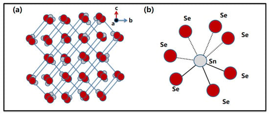
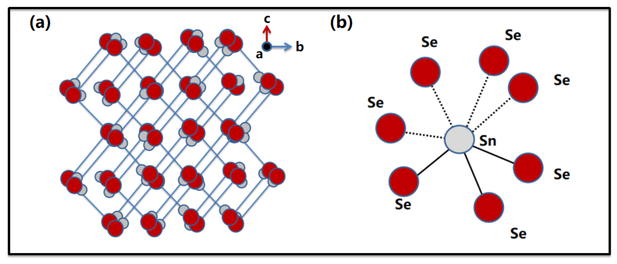
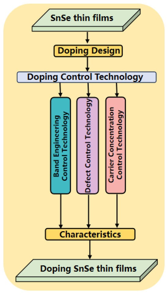
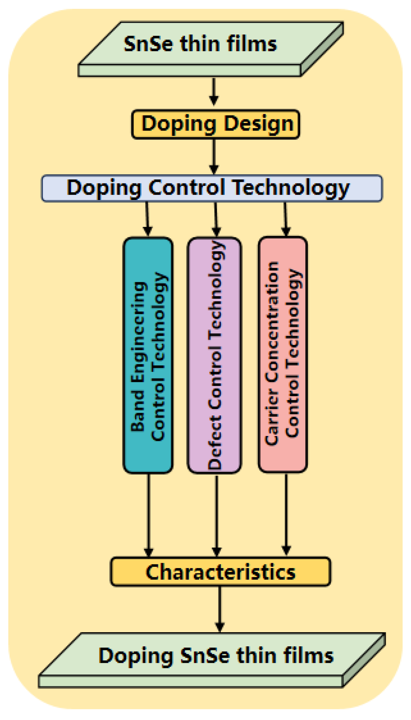
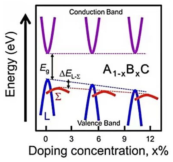
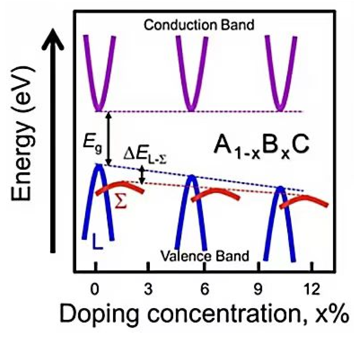
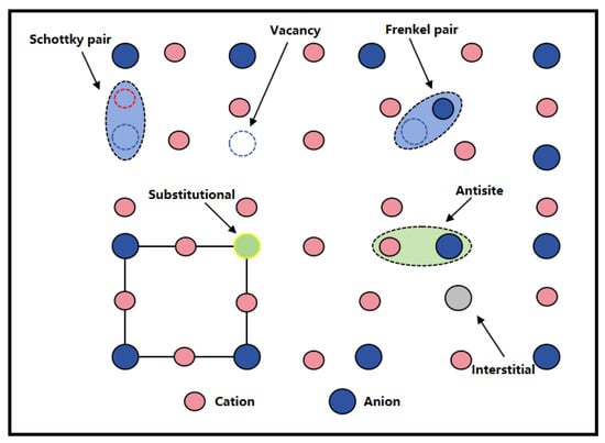
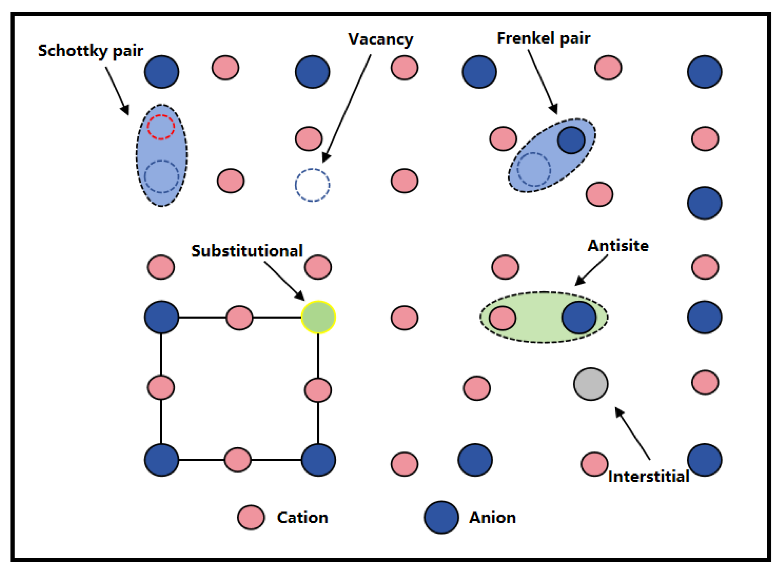
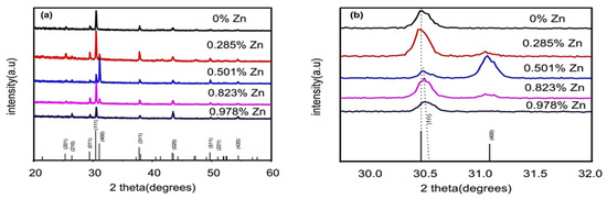
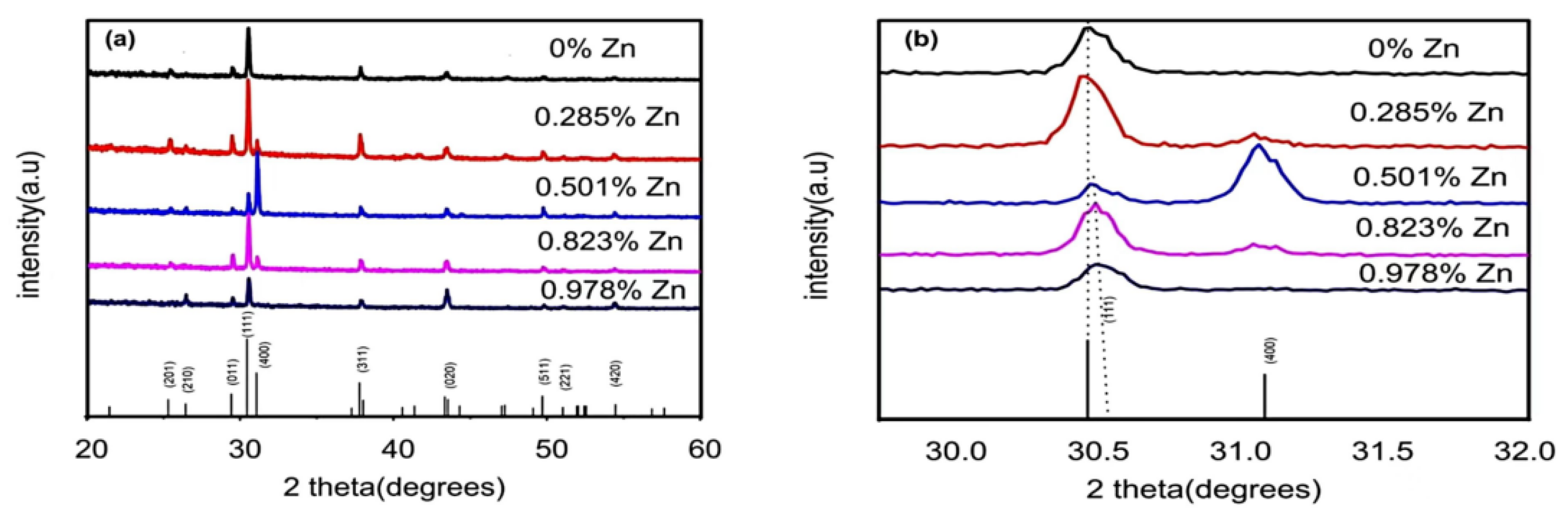
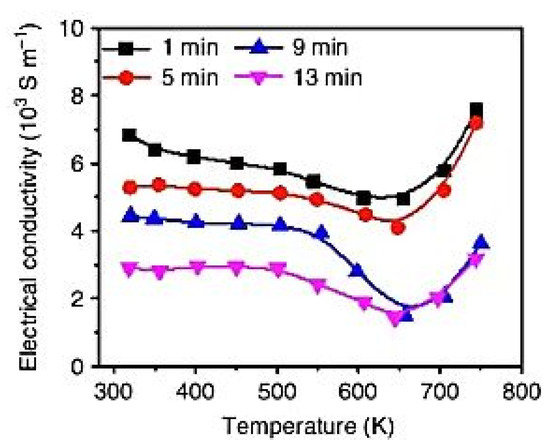
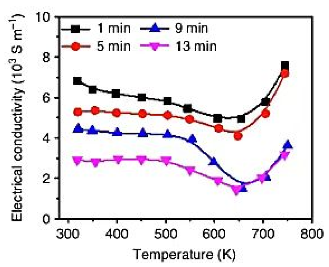
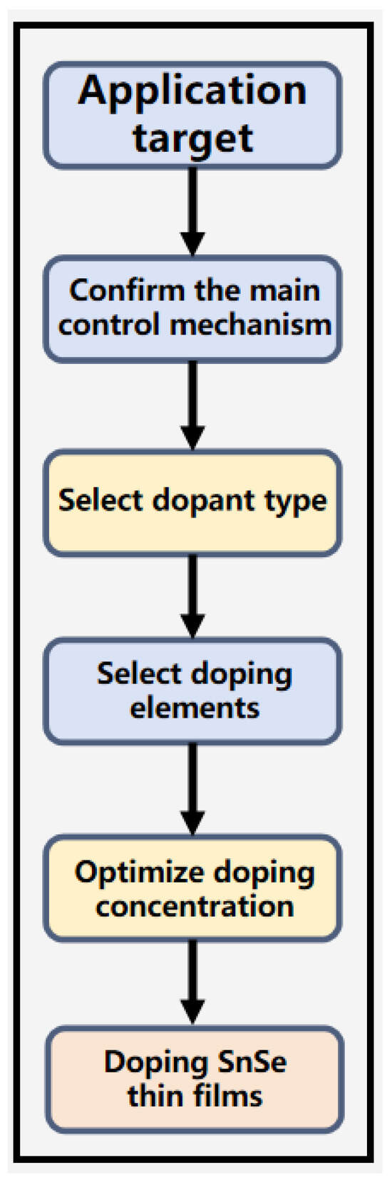
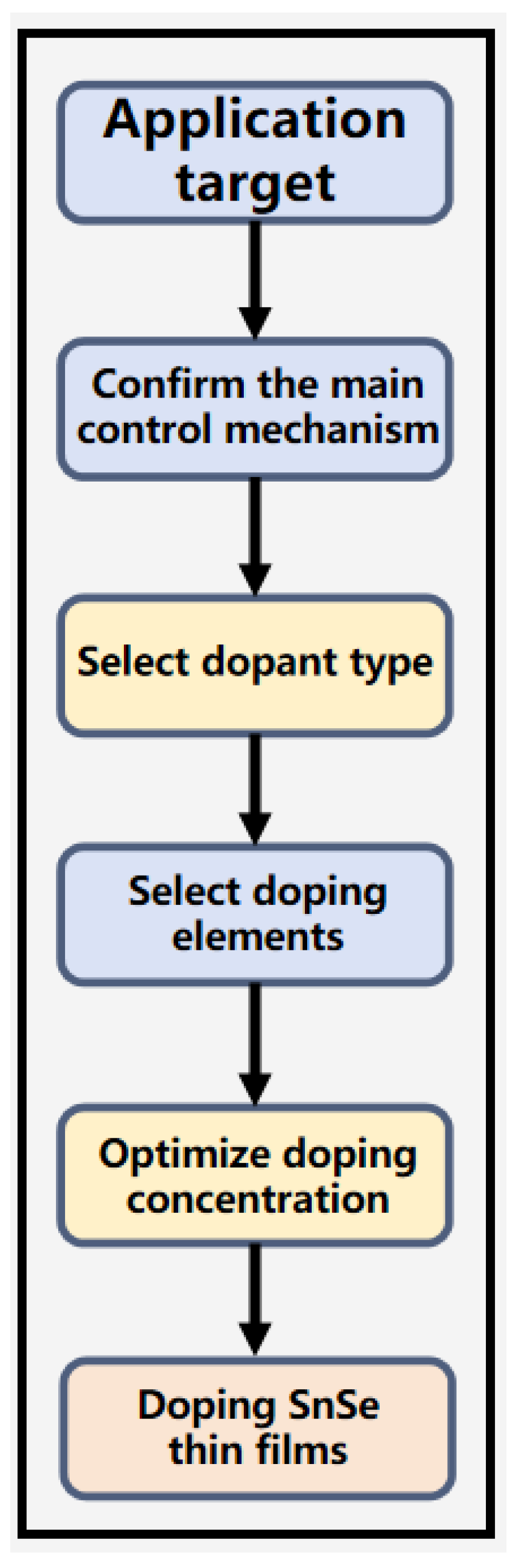
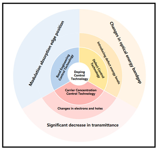
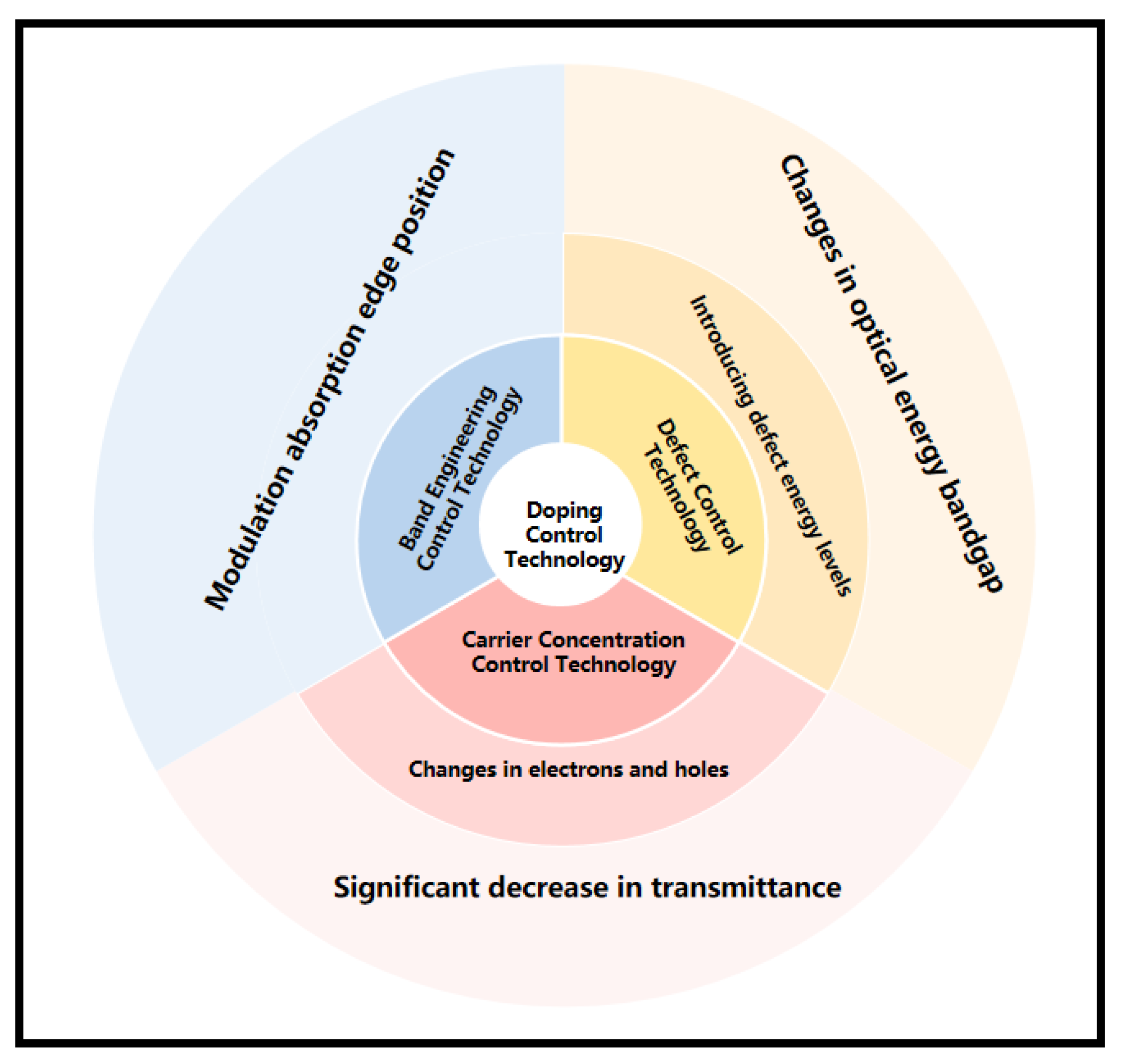

Disclaimer/Publisher’s Note: The statements, opinions and data contained in all publications are solely those of the individual author(s) and contributor(s) and not of MDPI and/or the editor(s). MDPI and/or the editor(s) disclaim responsibility for any injury to people or property resulting from any ideas, methods, instructions or products referred to in the content. |
© 2026 by the authors. Licensee MDPI, Basel, Switzerland. This article is an open access article distributed under the terms and conditions of the Creative Commons Attribution (CC BY) license.