


Abstract
Biomedical-grade stainless steel (316L) is susceptible to corrosion in human body fluids, and the subsequent release of metallic ions may contribute to adverse health effects. Silicon nitride (SiN), a biocompatible material, offers strong adhesion and serves as an effective barrier on metallic substrates, significantly reducing the corrosion rate of 316L stainless steel. The corrosion resistance of the SiN coating is influenced by the sputtering deposition parameters. In this study, SiN thin films were deposited at varying power levels to optimize the corrosion resistance of 316L stainless steel. Surface and electrochemical characterization techniques were employed. The findings demonstrate that the thin film deposited at 60 W exhibits the highest corrosion resistance, attributed to its reduced apparent porosity (1.3%).
1. Introduction
The global population is aging, becoming more susceptible to joint and mobility-related diseases. Common issues such as low back pain and neck discomfort, which can signal lumbar and cervical degenerative disk disease, affect all age groups [1,2,3]. However, age is not the only risk factor; even younger individuals with active lifestyles or those who have experienced traffic accidents face a higher risk for joint diseases.
Diseases such as arthritis and degenerative disk disease are typically managed with non-invasive treatments, including medication and physical therapy. When these approaches are no longer effective, surgical intervention and the implantation of orthopedic prostheses become necessary [4]. Orthopedic implants are commonly fabricated from metallic alloys such as cobalt chromium (CoCr), titanium alloy (Ti6Al4V), and stainless steel. Among stainless steels, SS316L is the most frequently used in orthopedic applications due to its cost-effectiveness, machinability, and corrosion resistance [5,6]. However, a significant limitation has been identified: stainless steel is susceptible to corrosion in the human body, leading to the release of cations and contamination of surrounding tissues with metallic debris [7,8]. This corrosion is exacerbated by the physiological environment, which contains aggressive ions such as bicarbonate , chloride (Cl−), and phosphate (), as well as organic acids and proteins, such as albumin [9]. These factors collectively promote the corrosion of metallic materials and can ultimately lead to implant failure [10,11].
The significance of using SS316L in orthopedic protheses arises from its composition, which contains iron, at least 16 wt% chromium, 14 wt% nickel, and 2 wt% molybdenum. These elements collectively enhance corrosion resistance. Nevertheless, the release of these elements can contaminate the human body, resulting in disease and potentially causing severe organ damage. Ortiz et al. [12] reported that SS316L is toxic to human fibroblasts, as nickel and chromium promote apoptosis, whereas iron may induce necrosis in certain cells. Implant-related allergic complications, primarily associated with nickel, are also frequently observed [13]. Moreover, the release of ions and alterations in surface overpotentials can disrupt normal cellular functions, affecting cell viability, proliferation, and membrane transport. The presence of released Cr ions has been shown to inhibit osteoblast mineralization [10]. Tang et al. [14] demonstrated that these adverse effects are exacerbated in 3D-printed components because the morphology and size of residual powder particles can interact with human cells, thereby intensifying the immunological response. Neuropsychiatric symptoms have also been investigated, with evidence indicating that the release of Cr metallic cations may contribute to depression and dementia in patients exposed to elevated chromium and cobalt levels [15]. Furthermore, the release of metal cations into body fluids can lead to pseudotumor formation and produce inflammatory responses through toxicity and allergic reactions [16,17].
These findings indicate the multiple risks that the population can present and constitute a significant challenge for the global health system. Consequently, there is an urgent need to develop new strategies to enhance the corrosion resistance of metallic alloys used in biomedical applications. Pathote et al. [18] report that although SS316L exhibits promising corrosion resistance, its performance can be further improved by applying surface coatings. Spajic et al. [19] employed alumina and hafnia films to enhance the biocompatibility of Ti and SS316L, demonstrating that these coatings do not induce harmful effects on human bone marrow-derived mesenchymal cells.
Silicon nitride (SiN) is a non-oxide ceramic material characterized by high chemical stability, superior mechanical properties, established biocompatibility, and bacteriostatic activity. These attributes make SiN a promising candidate for use as a protective barrier coating to improve the corrosion resistance of metallic implants [20].
Several research groups have used SiN in metal processing, the aerospace industry, and structural applications through methods such as powder metallurgy, nitriding of silicon powders, and coating processes on metallic substrates [21]. Table 1 summarizes the application techniques of SiN.
Table 1.
Methods for applying SiN thin films and coatings.
As shown in Table 1, SiN can be deposited using several techniques. Among these, sputtering is a particularly suitable method, enabling the formation of thin films with controllable characteristics, including uniform thickness, strong adhesion to the substrate, and low deposition temperatures [34,43]. However, the film’s properties are influenced by the deposition parameters. Therefore, identifying the optimal set of RF sputtering process variables is essential to maximize the corrosion resistance of the coated system.
SiN exhibits physicochemical properties that position it as a promising material for bone tissue engineering, as supported by both in vitro and in vivo studies [44]. Guo et al. [45] demonstrated that SiN possesses osteogenic properties, promoting cell proliferation and osteoblastic differentiation. These characteristics are advantageous for implants, as they may reduce the risk of implant failure associated with poor integration between metallic implants and bone tissue. In addition, SiN enhances the biological environment at the application site by inducing osteogenic and antimicrobial properties, thereby facilitating successful healing and reducing infection rates in peri-implant regions [21].
Although the mechanisms underlying the beneficial effects of SiN in the peri-implant region are not yet fully elucidated, some studies indicate a relationship between nitric oxide (NO) release from the SiN surface and its osteogenic effects [21]. Moreover, particles released from SiN exhibit a lower biological impact on human cells than those from CoCr or Ti6Al4V [46].
In this work, a set of SS316L steel samples coated with SiN and deposited at various radiofrequency (RF) power levels was characterized using surface and electrochemical techniques. To replicate the corrosive environment of the human body, electrochemical measurements were conducted in a strong oxidative body fluid solution (PBS + 2% H2O2) at 37 °C. It is hypothesized that increasing RF power during sputtering of SiN enhances ad-atom mobility, resulting in denser and lower-porosity films with improved barrier properties against ionic transport in strong oxidative biological environments.
2. Experimental Methodology
A commercial-grade SS316L rod was sectioned into 12 mm-diameter, 3 mm-thick disk coupons using waterjet cutting. The resulting samples were sequentially ground with abrasive papers ranging from 120 to 1000 grit and polished to a mirror finish with 0.1 μm alumina. To remove surface contaminants, the coupons were ultrasonically cleaned in trichloroethanol (Cl3C-CH2OH) and acetone (CH3COCH3) for 15 min.
Samples were placed in the sputtering chamber of custom-built magnetron sputtering equipment developed by the Silicon Photonics Group at the Institute of Physics at UNAM. The target composition consisted of 99% Si3N4 and 1% Si. The target is commercially available (Abletarget, Nanjing, China), and it is 5 mm thick with a 2.5 cm diameter. The chamber was evacuated using both a rotary mechanical pump and a turbomolecular pump until a base pressure of 5 × 10⁻⁵ Torr was reached before deposition. Following the cleaning procedure, argon gas (99.99%) was introduced to achieve a working pressure of 4 × 10⁻² Torr. The substrate temperature was maintained at 300 °C, and the target-to-substrate distance was fixed at 50 mm. On the configuration of this equipment, the target and substrate were static and parallel. Once the sputtering chamber was cleaned, the deposition of the thin film was conducted for 1 h. The frequency source used was 13.56 MHz (R301 SEREN Industrial Power Systems, Vineland, NJ, USA). All parameters were held constant except for the RF power, which varied from 10 to 60 W to evaluate its influence on the thin film’s properties and performance.
The SiN-coated samples were characterized using a JSM-JEOL J7800F scanning electron microscope (SEM) (Tokio, Japan) operated at 10 kV with secondary-electron detection coupled to an EDS detector (X-Max, Oxford Instruments) (Buckinghamshire, UK). To identify the N signal, an acceleration voltage of 5 kV was used. Surface topography was assessed using a JEOL JSPM 4210 atomic force microscope (AFM). The SEM and AFM data were analyzed using ImageJ 1 and Gwyddion 2.70, respectively [47]. Composition and crystallinity were assessed using a micro-Raman spectroscopy system (JEOL) with a laser beam of 532 nm. The fractal dimension was determined using the box-counting method [48] implemented in a custom Python 3.14.7 program. Prior to analysis, the SEM micrographs were binarized.
Electrochemical measurements were performed using an Autolab PGSTAT 302N and a three-electrode electrochemical cell (200 mL). The sample served as the working electrode, a large graphite sheet served as the counter electrode, and an Ag/AgCl electrode served as the reference electrode. A Luggin capillary was used to minimize the contamination of the reference electrode. The exposed confined area was 1.12 cm2 and was sealed using a polymeric O-ring. A strong oxidative body fluid solution consisting of phosphate-buffered saline solution (PBS) containing 2% hydrogen peroxide, naturally aerated, was used as the corrosive electrolyte. The PBS was used since it keeps pH values and ionic strength close to physiological conditions; the classical composition is reported elsewhere [49,50]. Hydrogen peroxide was included due to its documented presence in inflammatory environments, such as post-surgical conditions [51]. The addition of H2O2 was carried out at the beginning of the test, and the evolution or decomposition of this species was not addressed. This addition was essential to increase the electrolyte’s aggressiveness and to generate data under severe oxidative conditions. The electrochemical cell was connected to a thermal bath to maintain the electrolyte at 37 °C. The cell design ensured that the corrosive electrolyte remained isolated from the thermal bath fluid.
Potentiodynamic polarization curves were obtained at a scan rate of 1 mV/s, with the potential swept from −500 to 800 mV versus the open-circuit potential (OCP) in the anodic direction. The Tafel slopes were acquired in the overpotential region of 50 to 150 mV around the Ecorr. Electrochemical impedance spectroscopy was conducted using a 10 mV rms perturbation signal over the frequency range 105 to 10−2 Hz, under OCP conditions and acquiring 10 points per decade, and results were validated using Kramers–Kronig relations. Prior to performing the electrochemical techniques, the samples were immersed for 3 h to allow stabilization. All measurements were conducted in a triplicate, using independent samples for each electrochemical technique.
3. Results and Discussion
3.1. Morphological and Topographical Characteristics of the SiN Thin Films
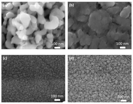
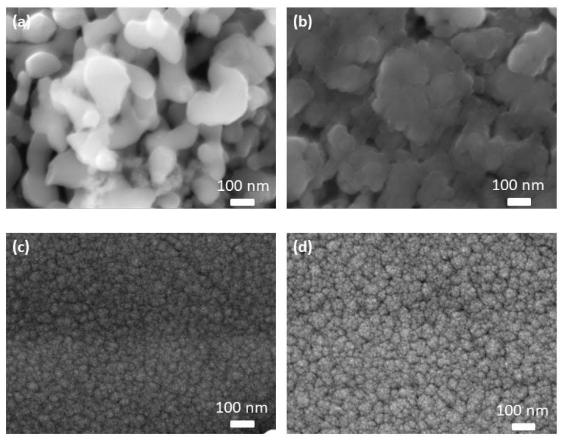
Figure 1 displays scanning electron microscopy (SEM) micrographs of silicon nitride (SiN) thin films deposited at varying radio frequency (RF) power levels. The morphology of these coatings is strongly influenced by the RF power applied during deposition. At 10 W (Figure 1a), the film exhibits elongated, vermicular particles and increased porosity due to loosely connected structures. In contrast, films deposited at 20 W (Figure 1b) demonstrate a more compact structure with oat-flake morphology. At this power, the initial formation of agglomerates and particle boundaries within the particles is evident. These RF power levels yield particles with greater length and width, a phenomenon attributed to fewer nucleation sites, which enables more uniform atomic deposition. Lower RF power limits ad-atom mobility, restricting SiN crystal growth into elongated and interconnected structures. When increasing RF powers to 40 and 60 W, the samples shown in Figure 1c and Figure 1d, respectively, display a densely packed particle distribution, with agglomerates becoming increasingly prominent at 60 W. Particle size decreases markedly at this power, resulting in a more refined and less porous structure characterized by smaller particles distributed across the surface.
Figure 1.
SEM micrographs of SiN sputtered samples at varying radio frequency (RF) powers: (a) 10 W, (b) 20 W, (c) 40 W, and (d) 60 W.
The mean particle sizes measured from SEM micrographs were 117.2, 97.3, 30.1, and 17.9 nm at 10, 20, 40, and 60 W, respectively. The substantial reduction in particle size from 117.2 to 17.9 nm as power increases from 10 to 60 W is attributed to an increased availability of nucleation sites and the atomic peening effect resulting from high-power energetic ion bombardment [52,53]. This mechanism enhances the supersaturation of ad-atoms on the surface, reduces the critical nucleation radius, and consequently promotes interrupted competitive growth while restricting particle development [54].
These findings demonstrate that the growth rate is strongly influenced by specific deposition conditions. Increasing RF power induces distinct morphological changes in the thin film. Higher RF power modifies the layer morphology by enhancing ad-atom mobility and facilitating the formation of a compact, dense structure.
The nanostructured thin films presented in Figure 1c,d closely resemble the micrographs reported by several research groups [48]. In contrast, the morphology and appearance depicted in Figure 1a correspond to those commercially available nanosized suspended SiN particles, as described by Lai et al. [55]. This finding is noteworthy, as RF magnetron sputtering enables the deposition of nanostructured thin films with lower porosity than some commercially available powder alternatives [55]. On the other hand, the thickness of the sample was previously reported in a publication of the authors, indicating that the maximum thickness is close to 310 nm [56]. Table S1 and Figure S1 in the Supplementary Materials show the qualitative elemental composition and thickness of the thin films, indicating that they are composed of Si and N. It is necessary to remark that these results are qualitative since the low thickness of the thin film and the low elemental weight make it difficult to properly indicate the exact wt. % of the N content. This is a limitation in the case of using EDS in a quantitative manner since signals emitted by low-weight elements can be weak or overlap, making it difficult to properly identify the material’s elemental composition.
The change in RF power modifies not only surface features of the deposited thin film, as discussed above, but also the chemical characteristics of the film. According to Barrera et al. [28], the decrease in N occurring as RF power is enhanced is observed in coatings deposited on silicon substrates. Also, the thickness of the SiN thin film (310 nm) [56] is in the range of the growth rate previously reported [28], acting like a comparative reference, leaving aside the substrate composition.
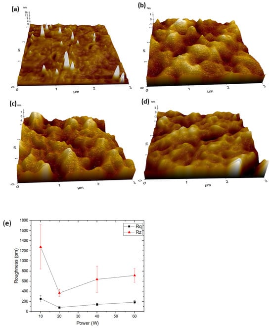
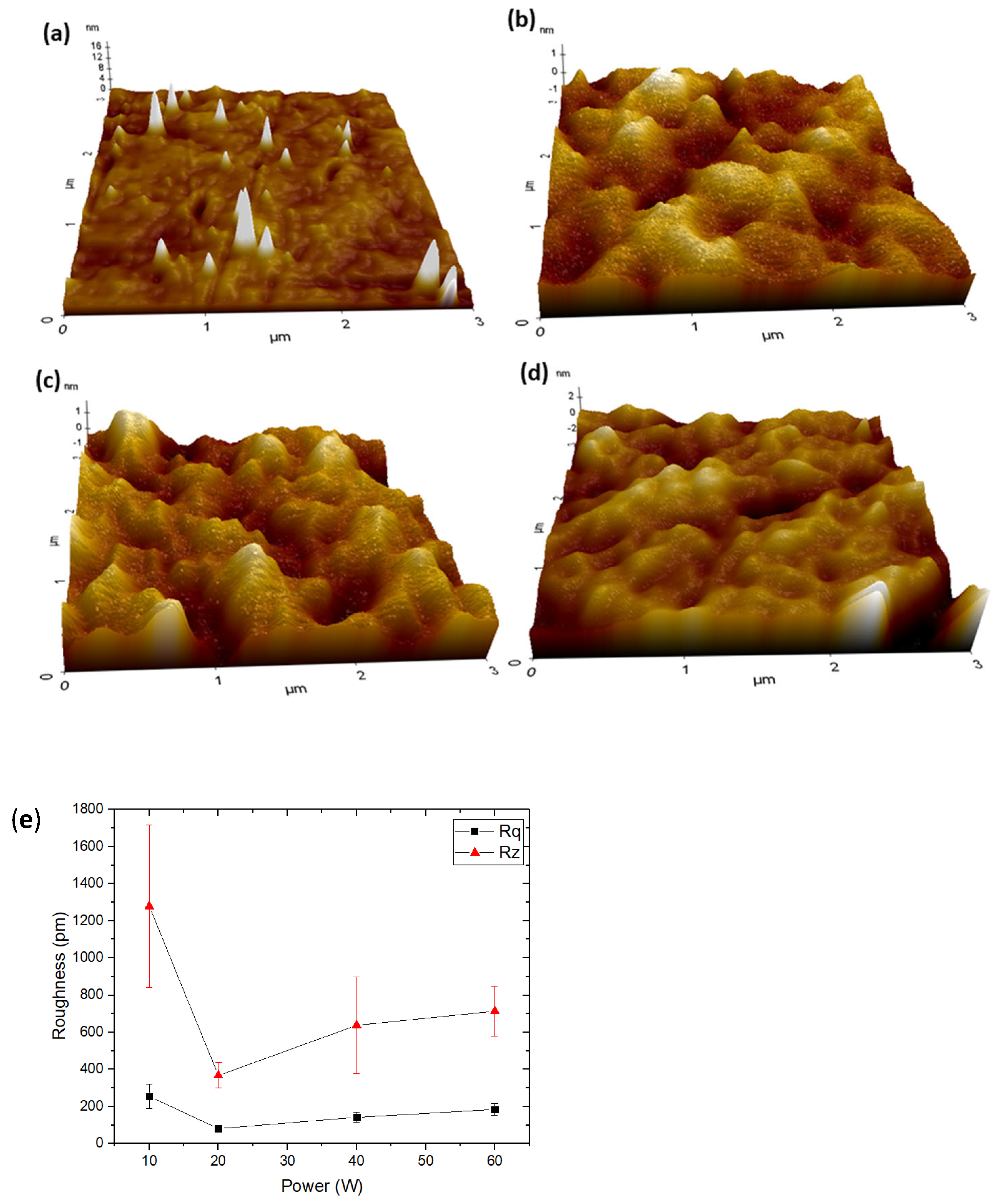
Atomic force microscopy (AFM) was used to characterize the surface morphology of the samples (Figure 2). The surface displays a granular structure, and the distribution of these granules varies with the applied radio frequency (RF) power.
Figure 2.
Surface topography of samples coated with SiN thin films at varying deposition powers: (a) 10 W, (b) 20 W, (c) 40 W, and (d) 60 W. (e) Surface roughness of the samples.
At 10 W (Figure 2a), the sample displays pronounced isolated peaks, with Rz values approaching 1.2 nm. This observation suggests island-like nucleation, characterized by three-dimensional islands and significant empty spaces between them, indicative of low ad-atom mobility. Figure 2b, Figure 2c and Figure 2d, corresponding to 20, 40, and 60 W, respectively, demonstrate that increasing RF power imparts greater kinetic energy to the ad-atoms, thereby enhancing their surface diffusion length. Analysis of SEM micrographs (Figure 1) and AFM data (Figure 2) indicates that the evolution of the SiN thin film aligns with the Volmer–Weber model, which involves the nucleation and growth of crystals until coalescence occurs [57,58]. At 20 W, the surface topography becomes rougher, with some flattened areas. At 40 W, the surface exhibits increased roughness, with numerous small-diameter particles coalescing to fully cover the steel substrate. The sample deposited at 60 W is even rougher and exhibits reduced porosity. Variations in RF power levels alter ad-atom mobility, influencing the morphology of the resulting thin film.
The Z-axis scale in the plots of Figure 2 indicates that the 10 W sample exhibits a maximum peak height of 12 nm. As RF power increases, the peak height decreases.
On the other hand, the average surface roughness (Ra) [59] is a parameter that represents surface morphology in the vertical dimension, showing values of 0.48, 0.35, 0.33, and 0.30 nm for the SiN/SS316L samples coated at 10, 20, 40, and 60 W, respectively. In comparison, the Rq and Rz parameters represent the root-mean-square roughness and the maximum height of the profile, respectively. Rq reflects the average height deviations from a mean line, while Rz measures the average distance from the highest peak to the lowest valley. Figure 2e shows a summary of these parameters. The sample coated at 10 W exhibits the highest Rz values and the greatest dispersion, consistent with the morphology observed in SEM micrographs, in which the growth model promotes localized, elongated particle growth. Excluding the 10 W sample, a linear relationship is observed as the applied power increases. The Rq values demonstrate reduced roughness, suggesting that the coating morphology becomes smoother, although a slight increase in peak height persists. Changes in Rz further indicate that the surface topography evolves, leading to greater variation in the height profile of the 40 W sample. For the 60 W sample, the Rz value slightly increases but the error bar can suggest that more particles form and cover the valley regions.
The quantitative analysis shown in Figure 2e indicates that interface roughness does not increase linearly. Instead, there is an abrupt decrease when the power increases from 10 to 20 W. At 10 W, the Rq and Rz values reach their maximum (234.4 and 1265.4 pm, respectively), accompanied by the largest standard deviation. This behavior is attributed to the formation of isolated three-dimensional islands, which is characteristic of the initial stage of the Volmer–Weber growth model [60]. At 20 W, increased bombardment energy enhances the surface mobility of ad-atoms, promoting the coalescence of nuclei and resulting in decreased roughness (Rq approximately 141.6 pm), thereby producing a more uniform basal topography. The slight increase in Rz values at 40 W and 60 W is attributed to growth competition among previously coalesced particles, which compact the film and reduces final porosity through a columnar overgrowth mechanism [54]. This behavior is attributed to increased radio frequency (RF) power, which modifies surface coverage by altering both the deposition rate and the thin film morphology. Elevated RF power results in a higher deposition rate, leading to improved surface coverage and reduced roughness, as demonstrated by the surface scan profiles in Figure S2, Supplementary Materials. Morphological and surface topography analyses provide complementary and consistent information, thereby validating the characterization. Since the deposition was conducted using pure argon (Ar) without the addition of reactive gas, the process operates in a non-reactive mode and inherently avoids the hysteresis effects commonly observed in reactive sputtering [61].
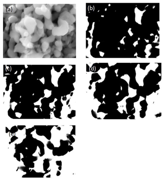
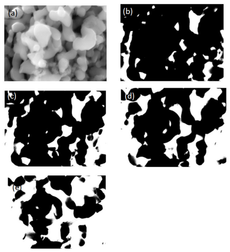
To clarify the scale-dependent complexity of SiN surface features, fractal dimension analysis was performed on the SEM micrographs shown in Figure 1. Representative binarized SEM micrographs (10W300) at various thresholds are displayed in Figure 3. Fractal dimension analysis reveals the hierarchical organization of the surface and quantitatively evaluates structural self-similarity across multiple scales [62]. Applying progressive thresholds facilitates the identification of sample morphology and highlights threshold-dependent changes in structural features. Threshold segmentation further enables the detection of persistent elements, indicating a fractal-like organization [62].
Figure 3.
Surface images of SS316L sample coated at 10 W and 300 °C at various threshold levels: (a) original SEM micrograph; (b) binarized at threshold of 0.3; (c) binarized at threshold of 0.4; (d) binarized at threshold of 0.5; (e) binarized at threshold of 0.6.
Figure 3a displays the original scanning electron microscopy (SEM) micrograph of the sample coated at 10 W. Figure 3b–e present binarized images generated using threshold values from 0.3 to 0.6. Progressive threshold segmentation analysis, as shown in Figure 3b–e, serves as a topographic filter that isolates morphological features of the film at different heights within the granular aggregates. At a low threshold value of 0.3, the analysis captures the interconnected base of the coalescing particles. As the threshold increases to 0.6, the optical shear plane shifts toward the peaks of the SiN, resulting in the fragmentation of the continuous area into smaller, isolated clusters. This phenomenon, in which substructures replicate the spatial distribution of the original macroscopic map (Figure 3a), is indicative of fractal growth systems governed by diffusion-limited aggregation (DLA) or competitive nucleation processes [63]. The stability, or power law, derived from the box-counting method applied to these binarization scales allows for precise determination of the fractal dimension (Df), offering a quantitative descriptor of intrinsic roughness and geometric complexity that conventional statistical parameters, such as Ra or Rq, cannot adequately capture [64].
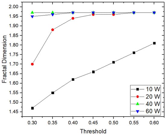
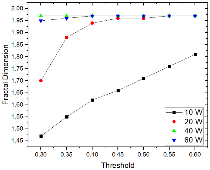
Figure 4 shows the fractal dimension (Df) values derived from the binarized samples, ranging from 1.46 to 1.98. Samples deposited at 10 W and 20 W show an increasing trend in Df with an increasing threshold. In contrast, samples deposited at 40 W and 60 W maintain an almost constant Df value in the range of 1.95–1.98. The Df values reflect the different degrees of surface complexity. Higher Df values indicate more intricate structures, while lower Df values correspond to smoother surfaces and simpler morphologies. These findings indicate that increasing the applied RF power results in greater morphological complexity of the deposited surface, consistent with higher-energy conditions. Comparable trends, in which high-energy conditions are associated with elevated Df values, have been documented by Vasconcelos et al. [62] and Petrovic et al. [65] during TiO2 film deposition.
Figure 4.
Fractal dimension (Df) at various threshold values applied to binarized scanning electron microscopy (SEM) micrographs.
Lower Df values are observed in the 10 W and 20 W samples. For the 10 W sample, this outcome reflects the formation of a film with reduced surface complexity but persistent structural features. These observations are consistent with the Atomic Force Microscopy (AFM) topography data and the roughness (Ra) measurements, which show a Ra of 0.48 attributed to localized surface peaks. In the 20 W sample, a similarly low Df value is recorded (Df = 1.70; threshold = 0.3); however, as the threshold increases, the Df values converge. Vasconcelos et al. [62] propose that this behavior may result from subtle features primarily distinguishing surface complexity, while larger-scale structures become less discernible at higher intensity thresholds.
The fractal dimension is consistent with the Volmer–Weber growth model. The high value observed in the 60 W sample indicates that, despite exhibiting low roughness, the coating possesses a dense and complex nanostructure, which is critical for functioning as an effective barrier against corrosion.
3.2. Raman Analysis of the Samples
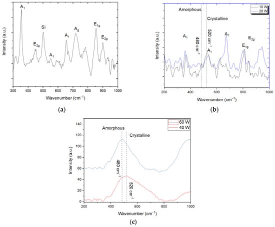
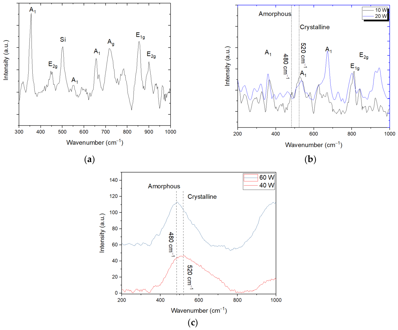
Raman spectroscopy was used to characterize the structural and compositional properties of the thin films deposited at various radiofrequency (RF) powers. Figure 5a presents the Raman spectra of the Si3N4 target, which exhibits characteristic peaks at 353 cm−1 (E vibration mode), 447 cm−1 and 453 cm−1 (E2g mode), 550 cm−1 and 655 cm−1 (A1 mode), 730 cm−1 (Ag mode), 856 cm−1 (E1g mode), and 899 cm−1 (E2g mode). The peak observed at 502 cm−1 indicates the presence of residual nanocrystalline silicon, while the positions at 353 and 447 cm−1 confirm the coexistence of α-Si3N4 and β-Si3N4 phases within the target material [66,67,68,69]. For comparative purposes, the Raman spectra of the SS316L target is shown in Figure S3, Supplementary Materials.
Figure 5.
Raman spectra of (a) SiN target, (b) thin film samples coated with SiN at 10 and 20 W, and (c) thin film samples coated with SiN at 40 and 60 W.
The structural evolution of the coatings was evaluated by analyzing the Raman spectra of the deposited SiN layers as a function of RF power, as shown in Figure 5b and Figure 5c for RF powers of 10 and 20 W and 40 and 60 W, respectively. The fitted peak parameters are summarized in Table 2. The spectral features near 520 cm−1 and 480 cm−1 are widely recognized as indicators of the crystalline and amorphous phases of SiN layers, respectively [70].
Table 2.
Raman peaks of the samples deposited at different RF powers.
As shown in Figure 5b, the Raman spectra for the films deposited at 10 W and 20 W retain the primary vibrational features of the SiN target (A1, E1g, and E2g modes), although the 10 W sample displays lower overall intensity. The nanocrystalline silicon peak originally found at 502 cm−1 disappears after deposition. For both low-power conditions, a dominant crystalline contribution is confirmed by peak 2, which is located at 529.9 cm−1 (10 W) and 530.4 cm−1 (20 W). The slight shifting of this peak relative to the standard crystalline reference (502 cm−1) is attributed to a significant accumulation of residual stress within the thin films [71].
Figure 5c presents the Raman spectra for 40 W and 60 W, which display broad peaks within the 400–800 cm−1 region, indicative of Si-Si bonding. The characteristic features of crystalline α- and β-Si3N4 are absent, with the primary contribution attributed to α–Si chemical bonding. Despite this behavior, the elemental analysis of the thin film using low-voltage acceleration in energy-dispersive spectroscopy (EDS) revealed low nitrogen content, confirming the presence of Si and N in the thin film [56].
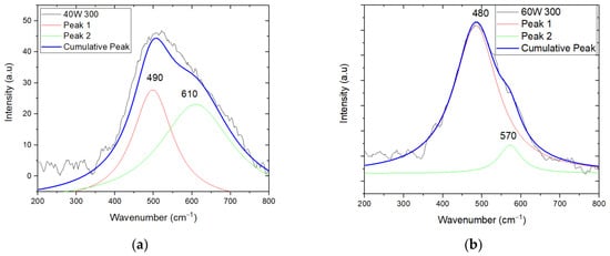
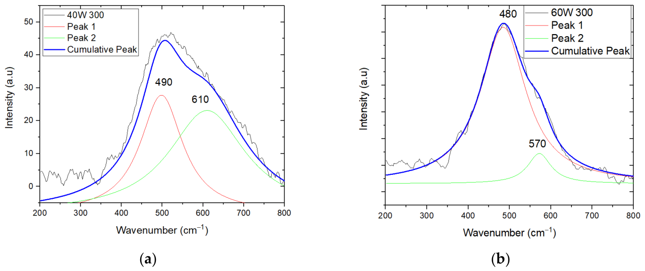
In contrast, increasing the RF power results in a pronounced structural transition toward a mixed contribution of an amorphous/nanocrystalline lattice. The thin film deposited at 40 W (Figure 6a) exhibits a broad, asymmetric spectral feature centered at 510 cm−1. Deconvolution of this feature reveals two distinct amorphous contributions: peak 1 at 490.3 cm−1 and peak 2 at 610.6 cm−1. The significant broadening of these modes, with full width at half maximum (FWHM) values of 57.08 and 94.21 cm−1, respectively, indicates substantial Si-Si bond-angle deviations due to increased internal lattice strain.
Figure 6.
Raman plots of the samples deposited at (a) 40 W and (b) 60 W.
At 60 W (Figure 6b), the amorphous characteristics become fully pronounced. The primary experimental peak shifts to 482.1 cm−1, confirming the predominantly amorphous nature of the layer. Concurrently, peak 2 shifts to 570.3 cm−1 with a drastically reduced area and a broadening of 784.69% and 23.32 cm−1, respectively, indicating a decrease in the secondary crystalline phases.
These findings demonstrate that the applied RF power plays a critical role in controlling the film microstructure. A crystalline lattice develops up to a specific RF power threshold. Beyond this threshold, the system transitions into an amorphous/crystalline material. This phase modification initially increases internal stress in the matrix due to bond distortions; however, as the lattice becomes highly randomized and predominantly amorphous at 60 W, the internal stress subsequently relaxes. On the other hand, further research and analysis techniques (XRD and TEM) are needed to clarify the amorphous/crystalline ratio in the thin film, and this issue will be discussed in a future publication of the authors.
3.3. Corrosion Behavior of the Samples
Potentiodynamic Polarization (PDP) Analysis
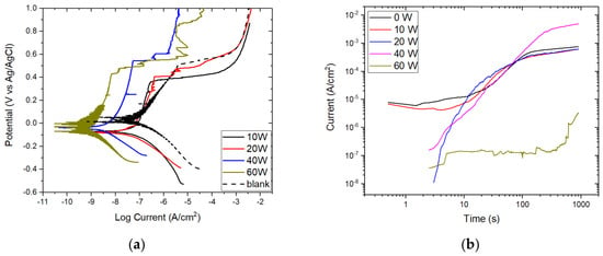
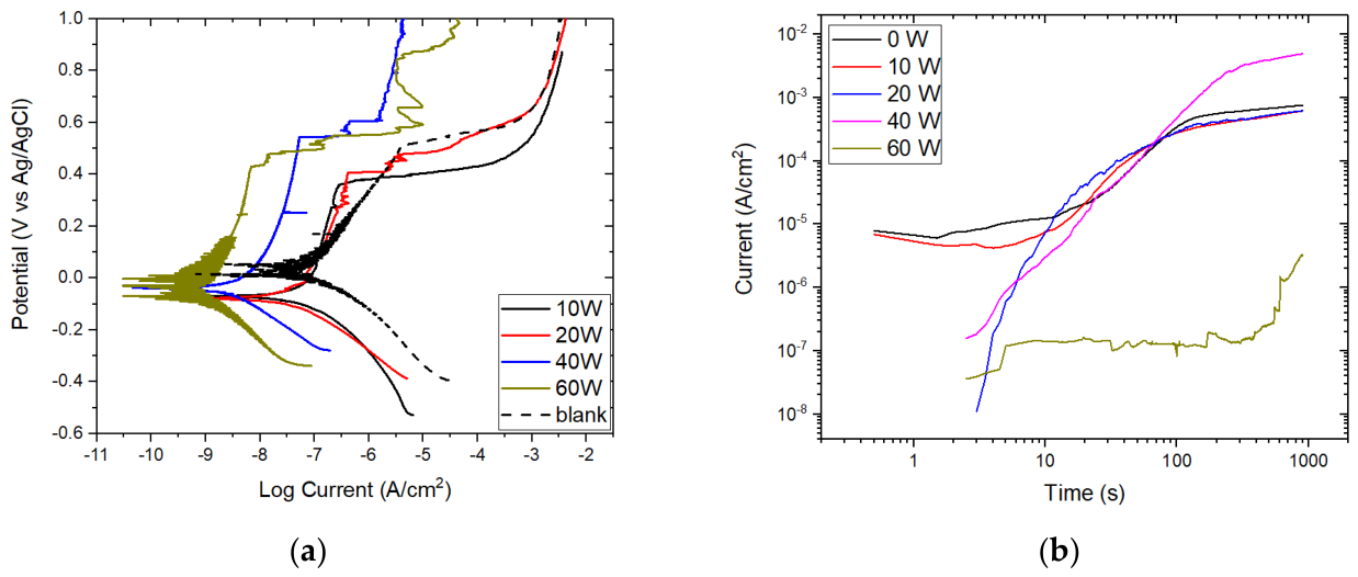
The corrosion behavior of 316L stainless steel samples was assessed in phosphate-buffered saline (PBS) solution at 37 °C using potentiodynamic polarization (PDP) curves, chronoamperometry, and electrochemical impedance spectroscopy (EIS). Figure 7a demonstrates that the PDP curves exhibit consistent qualitative behavior under all tested conditions. The cathodic region appears below the corrosion potential, while the anodic reaction domain begins once the potential surpasses this value. Oxygen reduction governs cathodic behavior, whereas the anodic region involves oxidation of the metallic substrate and the release of metal cations. Table 3 summarizes the electrochemical parameters obtained from these curves. Table S2 shows the determined Tafel slopes.
Figure 7.
(a) Potentiodynamic polarization curves of the 316L stainless steel coated with SiN thin films using different RF power. (b) Log–log representation of the potentiostatic curves of the SiN-coated coupons.
Table 3.
Parameters of the polarization curve.
The overall corrosion performance of 316L stainless steel varies significantly with the RF power used during thin-film deposition. Upon depositing the SiN layer, shifts toward more negative values. This shift is directly associated with the presence of silicon nitride on the substrate surface, consistent with the literature reporting a standalone SiN starting with an value near −200 vs. Ag/AgCl [71]. In comparison, the blank substrate exhibits an value of approximately vs. Ag/AgCl.
The corrosion current density () decreases notably after the application of the SiN thin film. As the RF sputtering power is scaled up, drops progressively down to the order of , which represents a reduction of nearly two orders of magnitude relative to the control sample ().
Furthermore, the rupture potential () in the anodic scan shows a slight increase. The improvement in overall corrosion resistance remains pronounced, as the passive current density decreases upon thin-film deposition, confirming the robust protective effect of the SiN barrier on the stainless steel substrate.
On the other hand, the Tafel slopes (Table S2) indicate that anodic dissolution of the metallic substrate is retarded with the increase in the RF power used for the deposition of the SiN thin film. Also, the cathodic slope remains constant, indicating that the reduction mechanism remains unchanged.
El Baakili et al. [72] reported an value in the range of for 316L stainless steel coupons coated with chitosan/bioactive glass after a 7-day immersion period in SBF at 37 °C, exerting a protective effect towards the metallic substrate. In comparison, our optimized SiN thin film deposited at the highest RF power (60 W) yields a sharp decrease in corrosion current, outperforming their barrier effect by up to three orders of magnitude.
A similar behavior was observed in the study by Sidane et al. [73], in which the authors evaluated 316L substrates coated with hydroxyapatite and silicon dioxide in PBS at 37 °C. Their cyclic voltammetry tests confirmed that the coating lowers the corrosion current density; however, their minimum recorded value remained in the range, which is higher than the values attained in this work.
On the other hand, Majee et al. [74] explored a sophisticated trilayered coating system (passive layer/electrophoretic ceramic/chitosan) on 316L stainless steel. The coating system was composed of a stainless steel passive layer, an electrophoretically deposited ceramic coating, and chitosan. The in vitro tests were carried out in SBF solution, and the in vivo tests were conducted in rabbits. Their in vitro tests in SBF reduced to , a value only slightly lower than our single-layer SiN film configuration ( at 60 W) (Table 3). Collectively, these outcomes underscore the efficacy of the proposed SiN coatings as promising candidates for mitigating corrosion-induced degradation of 316L stainless steel in demanding biomedical applications and enhancing its corrosion resistance.
To supplement the electrochemical analysis, the coatings’ structural integrity was quantified by calculating the apparent electrochemical porosity () using the following relation [75]:
where and represent the polarization resistances of the bare and coated substrates, respectively; denotes the potential difference between the coated and control samples’ conditions; and is the anodic Tafel slope. The data used for computing the apparent electrochemical porosity is shown in Table S3.
The calculated porosity data (Table 3) reveal that increasing the RF sputtering power systematically reduces the porosity of the resulting film. Specifically, operating at 60 W drastically reduces coating defects, lowering porosity to as low as 1.3%. This trend closely mirrors the behavior observed by Sidane et al. [73] when using double-layer capacitance measurements and, in magnitude, aligns with the data reported by Barres et al. [76]. This correlation confirms that the high-power SiN layer successfully restricts the exposed metallic surface area of the underlying steel sample.
To verify long-term stability against localized breakdown, the samples were constantly polarized in the transpassive region at vs. Ag/AgCl. Figure 7b displays the corresponding log–log transient curves. The current density drops significantly for the sample coated at 60 W, whereas it remains relatively unaltered and high for the 0 W, 10 W, and 20 W variations. This distinct behavior is fundamentally governed by the low porosity of the high-power coating, which curtails the available electrochemically active surface area. Consequently, the SiN thin film acts as an effective physical barrier that decreases corrosion during testing in the passive region potentials. This protection is highly relevant to biological applications; as demonstrated by Li et al. [10], localized corrosion on 316L stainless steel severely degrades the adhesion and morphology of bone marrow-derived mesenchymal stem cells, inducing cell membrane depolarization, localized cytotoxicity, and impaired mineral deposition adjacent to the pits.
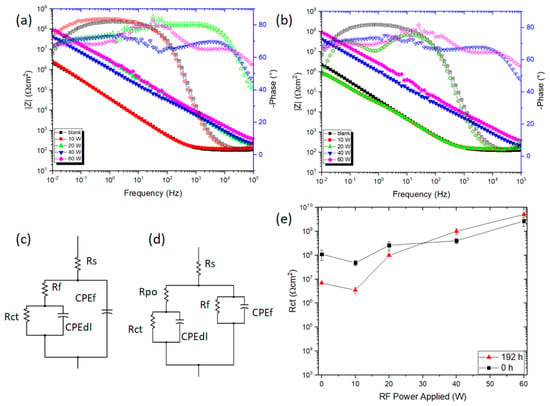
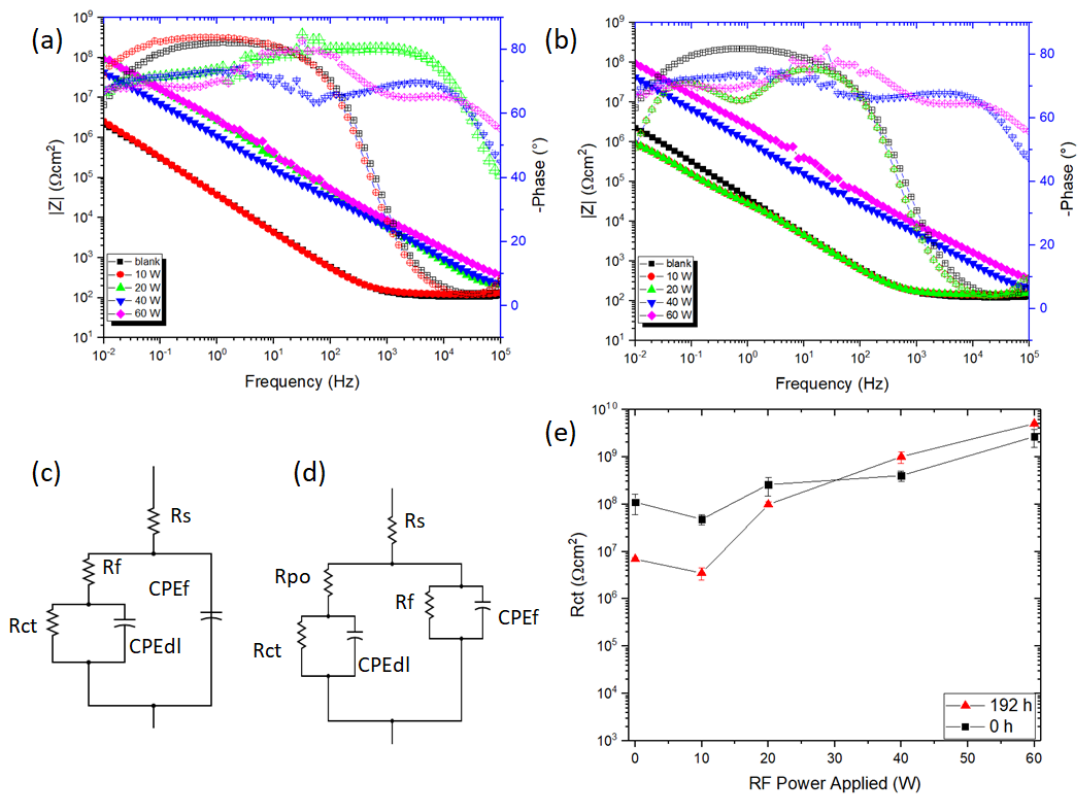
Figure 8 provides the Bode plots collected after (a) 48 h and (b) 192 h of continuous exposure to the PBS. Across all samples, the impedance modulus () increases as frequency decreases, indicative of a classic capacitive–resistive electrochemical system. On the other hand, the phase angle plot shows a variable response with applied coating power, revealing one time constant for the blank and 10 W-coated samples, and three time constants for the 20, 40, and 60 W-coated samples.
Figure 8.
Bode plots of the samples immersed in 2% H2O2-PBS at (a) 48 h and (b) 192 h at 37 °C. The electrical equivalent circuits used are shown in (c,d). (e) Charge transfer resistance of the corroded samples.
As the frequency sweeps across a specific frequency range, the corresponding electrochemical processes can be identified. In the high-frequency region, the electrolyte/coating interface is identified. The electrochemical response in the mid-frequency region is related to the response of the ceramic thin film, while the lower-frequency contribution is associated with the charge transfer and double-layer capacitance in the underlying stainless steel substrate.
Deposition of the SiN coating at powers exceeding 20 W raises the impedance modulus significantly, achieving values on the order of . This represents an enhancement of two orders of magnitude over the blank and 10 W samples.
Temporal evolution differs across the following conditions. The 20 W coating exhibits poor stability; its values decrease over time, eventually matching those of the control and 10 W samples. At 192 h of immersion, its protective capacity is fully compromised. This decay is corroborated by the phase angle profile, which transitions from a single broad phase peak to two distinct time constants, indicating severe film breakdown, and it can be related to the permeation of the electrolyte into the interconnected pores. The 40 W and 60 W coatings maintain highly stable impedance responses throughout the entire 192 h immersion matrix. This exceptional stability denotes superior protection that successfully thwarts electrolyte permeation, a direct consequence of their ultra-low porosity arrays. This is attributed to the coating’s lower apparent porosity, as evidenced by the apparent electrochemical porosity values in Table 3 and the SEM micrographs.
To quantitatively interpret the relaxation processes, the experimental EIS data sets were modeled using equivalent electrical circuits (EECs). The circuit configuration was adapted to reflect the physical state of each system. For the control and 10 W samples, the EECs are shown in Figure 8c, featuring two parallel resistor–capacitor (RC) pairs arranged in series. This configuration matches equivalent circuits for bare metal surfaces and is used since the first RC pair reflects the response of the thin film coating and the second reflects the charge transfer effect. Also, the wide frequency range duration suggests the superposition of at least two electrochemical processes. In comparison, for the 20 W, 40 W, and 60 W samples, the EECs are fitted using the circuit shown in Figure 8d.
In these circuits, represents the solution resistance, represents the intrinsic coating resistance, and is the constant phase element accounting for the non-ideal capacitive response of the SiN film. These elements were considered for the electrochemical processes carried out in the thin film without interconnection of the pores. The second RC pair considered was as follows: represents the charge transfer resistance, and is the phase constant element related to the redox reactions carried out at the metal/electrolyte interface. represents the complex nanostructured porosity of these high-power thin films, which creates a lattice form of fine, interconnected pores. For the case of a blank sample, and represent the resistance of the passive film and the constant phase element of the passive layer, respectively. The Cole–Cole exponent (,) consists of parameters used to approximate the response of the CPE elements and can have values approaching 1, which imply near-pure capacitive behavior, and negative values as low as −1, which signify inductive behavior, while and a value of 0.5 points to classic Warburg diffusion control. The complete fitting results are compiled in Table S4 of the Supplementary Materials.
The differences in the coating characteristics involve the use of distinct equivalent electrical circuits (EECs) since the electrochemical response of the blank sample can be fitted to a two-pair RC circuit, as evidenced by the work reported by El Baakili et al. [72]. A second EEC was also used to fit the results, and its use is justified by the higher nanostructured porosity of the thin film, which introduces an additional RC pair of elements, as described in references [54,73]. Deposition of the thin film at 10 W yields a porous structure with approximately 23% porosity, as shown in Table 3, thereby allowing the use of the same EEC. On the other hand, the decrease in porosity at higher RF power is related to the nanostructured characteristics of the thin film (Figure 1), which leads to the formation of interconnected pores with small diameters, thereby justifying the use of the element Rpore.
Figure 8e tracks the specific evolution of the charge transfer resistance () as a function of processing power. At the exposure onset (), scales directly with RF power, jumping from for the control sample to for the 60 W sample. Following 192 h of continuous immersion, the values for the blank, 10 W, and 20 W conditions degrade by nearly an order of magnitude, dropping into the range. Conversely, the 40 W and 60 W variations display a slight upward trend or stabilization in their responses after long-term immersion. This confirms that optimizing the RF deposition power to 60 W yields a dense, high-quality SiN thin film with ideal barrier properties, providing long-term electrochemical protection for the underlying stainless steel.
In summary, the attributed mechanism of protection of the SiN on SS316L exposed to a PBS with high oxidative characteristics relies on the synergic effect of the coating thickness and a decrease in the interconnected porosity along the coating promoted by the thin-film deposition that blocks the metallic substrate from the corrosive environment. This behavior is related to the thickness of the deposited thin film; it is also suggested that it contributes to diminishing the interconnected porosity of the layer. Since the barrier effect is also promoted by the interconnected porosity, the presence of lower porosity indicates that besides the surface porous area being smaller, the electrolyte can pass through a more “tortuous” path, where interconnectivity decreases as RF power increases. Then, the thickness of the coating promoted by the higher RF power mainly contributes to the corrosion protection of the steel substrates. Additionally, SiN is an inert material that scarcely interacts with the environment if at all [71]. This behavior probably reduces the effect in the corrosion resistance promoted by the crystalline or amorphous features of the thin films that can be determined in other types of coatings; for example, in the case of metallic Ni-P coatings, corrosion resistance varies according to the amorphous grade promoted by thermal treatment [77]. However, further characterization is necessary to clarify this issue and determine the effect of the crystalline/amorphous ratio on the corrosion behavior of the Si and N ceramic coating.
4. Conclusions
In this work, we demonstrate that applying silicon nitride (SiN) thin films via radiofrequency (RF) sputtering is a highly effective strategy for mitigating the corrosion susceptibility of biomedical SS316L stainless steel in highly oxidative environments. The results confirm that RF deposition power is the critical process parameter governing both the microstructure and the protective barrier properties of the coating. The growth of SiN films consistently follows the Volmer–Weber model.
At low power levels (10 W and 20 W), the limited mobility of ad-atoms results in isolated crystalline structures with elongated morphologies and high porosity. Increasing the power to 40 W or 60 W enhances the energy of the ionic bombardment, thereby increasing the surface mobility of atoms and multiplying the number of nucleation sites. This process induces a substantial reduction in particle size (from 117.2 to 17.9 nm) and promotes a complete structural transition toward a predominantly amorphous, dense, and low-porosity matrix.
Fractal dimension analysis quantitatively corroborates that samples deposited at higher powers (40 W and 60 W) exhibit stable, maximum geometric complexity values (Df = 1.95–1.98) across the surface plane. This intricate nanostructured lattice, as validated by Raman spectroscopy, facilitates the effective sealing of microscopic channels and valleys.
Electrochemical potentiodynamic polarization tests indicate that the film optimized and deposited at 60 W provides maximum corrosion resistance under aggressive conditions (phosphate-buffered saline solution with 2% H2O2 at 37 °C). This optimization is achieved by reducing coating porosity to at least 1.3%. Consequently, the corrosion current density (Icorr) was reduced by nearly two orders of magnitude compared to the control sample, reaching the range of .
Consequently, adjusting the deposition power to 60 W enables the synthesis of nanostructured SiN thin films with an apparently dominant amorphous character and minimal porosity. This optimized coating serves as an effective physical barrier to ionic transport, significantly reducing the release of toxic metallic cations into the body and providing a robust means to extend the lifespan of stainless steel orthopedic prostheses.
Supplementary Materials
The following supporting information can be downloaded at: https://www.mdpi.com/article/10.3390/coatings16101135/s1, Figure S1: EDS spectra of the thin films: (a) 40 W, (b) 60 W; Figure S2: Line scan profile of the surface of the SiN coated samples: (a) 10 W, (b) 20 W, (c) 40 W, (d) 60 W; Figure S3: Raman spectra of the SS316L sample; Table S1: Elemental composition (EDS) of the samples; Table S2: Tafel slopes of the covered SS316L samples; Table S3: Data used to obtain apparent porosity; Table S4: Relevant parameters of the fitting to the EEC.
Author Contributions
Conceptualization: J.R.G.-P., Formal Analysis: J.R.G.-P., A.B.-P., A.L.-S. and A.R.-G., Investigation: J.R.G.-P., A.A.L.V., and C.Z.R.S., Methodology: J.R.G.-P., Project Administration: J.R.G.-P., A.B.-P., and A.R.-G., Validation: J.R.G.-P., A.R.-G., Visualization: J.R.G.-P., Writing—original draft: J.R.G.-P., Data Curation: A.A.L.V. and C.Z.R.S., Funding Acquisition: A.B.-P. and A.L.-S., Resources: A.B.-P. and A.R.-G., Supervision: A.B.-P. and A.R.-G., Writing—review & editing: A.B.-P., A.L.-S. and A.R.-G. All authors have read and agreed to the published version of the manuscript.
Funding
This research received no external funding.
Institutional Review Board Statement
Not applicable.
Informed Consent Statement
Not applicable.
Data Availability Statement
The data presented in this study are available in the article or Supplementary Material.
Acknowledgments
J.R.G.-P. thanks the Universidad Nacional Autónoma de México Postdoctoral Program UNAM for his postdoctoral fellowship. This work was supported by the Universidad Nacional Autónoma de México Postdoctoral Program (POSDOC). The authors also acknowledge the technical assistance provided by Angel Flores Orozco, Samuel Tehuacanero Cuapa, Luis F. Garrido, and Carolina Bohórquez Martínez (IF-UNAM). This work was also supported by UNAM DGAPA-PAPIIT, grants IN-100325 and IN-101726.
Conflicts of Interest
The authors declare no conflict of interest.
References
- Available online: https://www.who.int/news-room/questions-and-answers/item/population-ageing (accessed on 20 September 2026).
- Chew, K.; Sharif, S.; Ahmad, A. The corrosion scenario in human body: Stainless steel 316L orthopaedic implants. Nat. Sci. 2012, 4, 184. [Google Scholar] [CrossRef]
- Du, X.; Zhou, Y.; Schümperlin, D.; Laganenka, L.; Lee, S.; Blugan, G. Fabrication and characterization of sodium alginate-silicon nitride-PVA composite biomaterials with damping properties. J. Mech. Behav. Biomed. Mater. 2024, 155, 106579. [Google Scholar] [CrossRef] [Scilit]
- Roy, A.; Bennet, A.; Pruitt, L. Feasibility of using diamond-like carbon films in total joint replacements: A review. J. Mater. Sci. Mater. Med. 2024, 35, 47. [Google Scholar] [CrossRef] [Scilit]
- Beddoes, J.; Bucci, K. The influence of surface condition on localized corrosion of 316L stainless steel orthopaedic implants. J. Mater. Sci. Mater. Med. 1999, 10, 389. [Google Scholar] [CrossRef] [Scilit]
- Erdogan, Y.; Ercan, B. Anodized nanostructured 316L stainless steel enhances osteoblast functions and exhibits anti-fouling properties. ACS Biomater. Sci. Eng. 2023, 9, 693. [Google Scholar] [CrossRef] [Scilit]
- Huang, X.; Zhou, K.; Ye, Q.; Wang, Z.; Qiao, L.; Su, Y.; Yan, Y. Crevice corrosion behaviors of CoCrMo alloy and stainless steel 316L artificial joint materials in physiological saline. Corros. Sci. 2022, 197, 110075. [Google Scholar] [CrossRef] [Scilit]
- Barlow, B.; Assini, J.; Boles, J.; Lee, Y.; Westrich, G. Short-term metal ions trends following removal of recalled modular neck femoral stems. J. Arthroplast. 2015, 30, 1191. [Google Scholar] [CrossRef] [Scilit]
- Hedberg, Y.; Odnevall, I. Metal release from stainless steel in biological environments: A review. Biointerphases 2015, 11, 018901. [Google Scholar] [CrossRef] [Scilit]
- Li, M.; Wu, J.; Geng, W.; Yang, Y.; Li, X.; Xu, K. Regulation of localized corrosion of 316L stainless steel on osteogenic differentiation of bone morrow derived mesenchymal stem cells. Biomaterials 2023, 301, 122262. [Google Scholar] [CrossRef] [Scilit]
- Mudali, K.; Sridhar, T.; Eliaz, N. Failures of stainless steel orthopaedic devices causes and remedies. Corros. Rev. 2003, 21, 231–267. [Google Scholar] [CrossRef] [Scilit]
- Ortiz, A.; Fernández, E.; Vicente, A.; Calvo, J.; Ortiz, C. Metallic ions released from stainless steel, nickel-free and titanium orthodontic alloys: Toxicity and DNA damage. Am. J. Orthod. Dentofac. Orthop. 2011, 140, e115–e122. [Google Scholar] [CrossRef] [Scilit]
- Baumann, C.; Crist, B. Nickel allergy to orthopaedic implants: A review and case series. J. Clin. Orthop. Trauma 2020, 11, S596–S603. [Google Scholar] [CrossRef] [Scilit]
- Tang, J.; Sang, Z.; Zhang, X.; Song, C.; Tang, W.; Luo, X.; Yan, M. Impacts of residual 3D printing metal powders on immunological response and bone regeneration: An in vivo study. J. Mater. Sci. Mater. Med. 2023, 34, 29. [Google Scholar] [CrossRef] [Scilit]
- Green, B.; Griffiths, E.; Almond, S. Neuropsychiatric symptoms following metal on metal implant failure with cobalt and chromium toxicity. BMC Psychiatry 2017, 17, 33. [Google Scholar] [CrossRef] [Scilit]
- Piotrowska, K.; Madej, M.; Ozimina, D. Assesment of the functional properties of 316L steel alloy subjected to ion implantation used in bio-tribological systems. Materials 2021, 14, 5525. [Google Scholar] [CrossRef] [Scilit]
- Mirzajavadkhan, A.; Rafieian, S.; Hasibul, M. Toxicity of metal implants and their interactions with stem cells: A review. Int. J. Eng. Mater. Manuf. 2020, 5, 2–11. [Google Scholar] [CrossRef] [Scilit]
- Pathote, D.; Jaiswal, D.; Singh, V.; Behera, C. Optimization of electrochemical corrosion behavior of 316L stainless steel as an effective biomaterial for orthopaedic applications. Mater. Today Proc. 2022, 57, 265–269. [Google Scholar] [CrossRef] [Scilit]
- Spajic, I.; Goncalves, M.; Monteiro, C.; Martins, C.; Pêgo, A.; Milosev, I. Biocompatibility and antibacterial properties of medical stainless steel and titanium modified by alumina and hafnia films prepared by atomic layer deposition. J. Mater. Sci. Mater. Med. 2024, 35, 68. [Google Scholar] [CrossRef] [Scilit]
- Du, X.; Lee, S.; Blugan, G.; Ferguson, S. Silicon nitride as a biomedical material: An Overview. Int. J. Mol. Sci. 2022, 23, 6551. [Google Scholar] [CrossRef] [Scilit]
- Liu, Z.; Wang, R.; Liu, W.; Liu, Y.; Ferng, X.; Zhao, F.; Chen, P.; Shao, L.; Rong, M. Recent advances in the application and biological mechanism of silicon nitride osteogenic properties: A review. Biomater. Sci. 2023, 11, 7003–7017. [Google Scholar] [CrossRef] [Scilit]
- Raju, K.; Moon, S.; Kim, M.; Kim, H.; Lee, H.; Cho, J. Cost-effective preparation of high-quality silicon nitride powders from silicon scrap through direct nitridation. Ceram. Int. 2023, 49, 34872–34879. [Google Scholar] [CrossRef] [Scilit]
- Duan, Y.; Liu, N.; Zhang, J.; Zhang, H.; Li, X. Cost effective preparation of Si3N4 ceramics with improved thermal conductivity and mechanical properties. J. Eur. Ceram. Soc. 2020, 40, 298–304. [Google Scholar] [CrossRef] [Scilit]
- Alemán, S.; Reyes, J.; González, J.; Días, S.; Ceja, L. Structural characterization by SEM and TEM of the sinter extruded Si3N4. MRS Adv. 2026, 11, 533–537. [Google Scholar] [CrossRef] [Scilit]
- Raju, K.; Moon, S.; Kim, M.; Cho, J.; Lee, H.-K. Catalyst-free synthesis of Si3N4 powders via direct nitridation of Si: Influence of particle size and nitridation parameters on the α-phase fraction. J. Korean Ceram. Soc. 2025, 62, 656–665. [Google Scholar] [CrossRef] [Scilit]
- Guan, J.; Wang, Y.; Cheng, L.; Xie, Y.; Zhang, L. Fabrication and characterization of short silicon nitride fibers from direct nitridation of ferrsilicon in N2 atmosphere. Materials 2018, 11, 2003. [Google Scholar] [CrossRef] [Scilit]
- Aguirre, T.; Cramer, C.; Martinez, M.; Richardson, D.; Moser, J.; Cakmak, E.; Wang, H.; Kunc, V.; Muth, T.; Klett, J. Strength and thermal shock resistance of porous reaction-bonded silicon nitride by direct nitriding of binder jet additively manufactured silicon. npj Adv. Manuf. 2025, 2, 13. [Google Scholar] [CrossRef] [Scilit]
- Barrera, E.; Rodriguez, A. Thin films of silicon nitride deposited at room temperature by non-reactive magnetrón sputtering: Radiofrequency power and deposition time influence on the formation of α-Si3N4 and its optical properties. Front. Phys. 2023, 11, 1260579. [Google Scholar] [CrossRef] [Scilit]
- Freitas, J.; Pimenta, S.; Rodrigues, V.; Silva, M.; Correia, J. Silicon nitride thin-films deposited by radiofrequency reactive sputtering: Refractive index optimization with substrate cooling in a nitrogen-rich atmosphere. Opt. Mater. 2024, 149, 115130. [Google Scholar] [CrossRef] [Scilit]
- De Luca, D.; Di Gennaro, E.; De Maio, D.; D’Alessandro, C.; Caldarelli, A.; Muso, M.; Koral, C.; Andreone, A.; Fittipaldi, R.; Di Meo, V.; et al. Tuning silicon nitride refractive index through radio-frequency sputtering power. Thin Solid Films 2021, 737, 138951. [Google Scholar] [CrossRef] [Scilit]
- Mokkedem, K.; Nouaouina, B.; Kechouane, M. Study of Hydrogenated Amorphous Silicon Nitride Deposition by DC Magnetron Sputtering Without Intentional Substrate Heating. Silicon 2026, 18, 1207–1213. [Google Scholar] [CrossRef] [Scilit]
- Batan, A.; Franquet, A.; Vereecken, J.; Reniers, F. Characterisation of the silicon nitride thin films deposited by plasma magnetron. Surf. Interface Anal. 2008, 40, 754–757. [Google Scholar] [CrossRef] [Scilit]
- Kulczyk, J.; Kelly, P.; West, G.; Clarke, G.; Ridealgh, J. Diffusion studies in magnetron sputter deposited silicon nitride films. Surf. Coat. Technol. 2014, 255, 37–42. [Google Scholar] [CrossRef] [Scilit]
- Hegedüs, N.; Balázsi, K.; Baläzsi, C. Silicon nitride and hydrogenated silicon nitride thin films: A review of fabrication methods and applications. Materials 2021, 14, 5658. [Google Scholar] [CrossRef] [Scilit]
- Ning, J.; Niu, C.; Tang, Z.; Sun, Y.; Yan, H.; Zhou, D. Optimizing the PECVD Process for Stress-Controlled Silicon Nitride Films: Enhancement of Tensile Stress via UV Curing and Layered Deposition. Coatings 2025, 15, 708. [Google Scholar] [CrossRef] [Scilit]
- Liu, L.; Liu, W.; Cao, N.; Cai, C. Study on The Performance of PECVD Silicon Nitride Thin Films. Def. Technol. 2013, 9, 121–126. [Google Scholar] [CrossRef] [Scilit]
- Cao, Y.; Zhou, J.; Ren, Y.; Xu, W.; Liu, W.; Cai, X.; Zhao, B. Study on effect of process and structure parameters on SiNxHy growth by in-line PECVD. Sol. Energy 2020, 198, 469–478. [Google Scholar] [CrossRef] [Scilit]
- Lisker, M.; Mahadevaiah, M.; Swami, K. Plasma-enhanced atomic layer deposition of silicon nitride for front-end-of-line applications. J. Vac. Sci. Technol. A 2023, 41, 042406. [Google Scholar] [CrossRef] [Scilit]
- Mameli, A.; Tapily, K.; Shen, J.; Roozeboom, F.; Lu, M.; O’Meara, D.; Semproni, S. Unfolding an Elusive Area-Selective Deposition Process: Atomic Layer Deposition of TiO2 and TiON on SiN vs SiO2. ACS Appl. Mater. Interfaces 2024, 16, 14288–14295. [Google Scholar] [CrossRef] [Scilit]
- Meng, X.; Byun, Y.; Kim, H.; Lee, J.; Lucero, A.; Cheng, L.; Kim, J. Atomic Layer Deposition of Silicon Nitride Thin Films: A Review of Recent Progress, Challenges, and Outlooks. Materials 2016, 8, 1007. [Google Scholar] [CrossRef] [Scilit]
- Ji, Y.; Kim, H.; Kang, J.; Choi, S.; Kim, K.; Kim, D.; Ellingboe, A.; Kim, H.; Yeom, G.; Kim, D. Plasma enhanced atomic layer deposition of silicon nitride using magnetized very high frequency plasma. Nanotechnology 2024, 35, 275701. [Google Scholar] [CrossRef] [Scilit]
- Zeghouane, M.; Lefevre, G.; Labau, S.; Hachemi, M.; Bassani, F.; Salem, B. Plasma-enhanced atomic layer deposition of silicon nitride thin films with different substrate biasing using Diiodosilane precursor. Mater. Sci. Semicond. Process. 2024, 184, 108851. [Google Scholar] [CrossRef] [Scilit]
- Rao, A.; Tiwari, S.; Goyat, M.; Chawla, A. Recent developments in magnetron-sputtered silicon nitride coatings of improved mechanical and tribological properties for extreme situations. J. Mater. Sci. 2023, 58, 9755–9804. [Google Scholar] [CrossRef] [Scilit]
- Tani, A.; Tsubouchi, H.; Ma, L.; Taniguchi, Y.; Kobayashi, Y.; Nakai, M.; Komasa, S.; Hashimoto, Y. Effect of silicon nitride coating on titanium surface: Biocompability and antibacterial properties. Int. J. Mater. Sci. 2024, 25, 9148. [Google Scholar] [CrossRef] [Scilit]
- Guo, L.; Gao, C.; Wang, F.; Wei, J.; Hu, J.; Xu, Y. Influence of content of silicon nitride nanoparticles into micro arc oxidation coating of titanium on bactericidal capability and osteoblastic differentiation. Surf. Coat. Technol. 2023, 458, 129346. [Google Scholar] [CrossRef] [Scilit]
- Heimann, R. Silicon nitride ceramics: Structure, synthesis, properties and biomedical applications. Materials 2023, 16, 5142. [Google Scholar] [CrossRef] [Scilit]
- Necas, D.; Klapetek, P. Gwyddion: An open-source software for SPM data analysis. Cent. Eur. J. Phys. 2012, 10, 181–188. [Google Scholar] [CrossRef] [Scilit]
- Ge, M.; Lin, Q. Realizing the box-counting method for calculating fractal dimension of urban form based on remote sensing image. Geo-Spat. Inf. Sci. 2009, 12, 265–270. [Google Scholar] [CrossRef] [Scilit]
- Bordbar-Khiabani, A. Simulated Body Fluids for Dental Implant Corrosion: A Practical Guide. Dent. J. 2026, 14, 292. [Google Scholar] [CrossRef] [Scilit]
- Gudic, S.; Vrsalovic, L.; Kvrgic, D.; Nagode, A. Electrochemical behavior of Ti and Ti-6Al-4V alloy in Phosphate Buffered Saline Solution. Materials 2021, 14, 7495. [Google Scholar] [CrossRef] [Scilit]
- Wittmann, C.; Chockley, P.; Singh, S.K.; Pase, L.; Lieschke, G.J.; Grabher, C. Hydrogen peroxide in inflammation: Messenger, guide, and assassin. Adv. Hematol. 2012, 2012, 541471. [Google Scholar] [CrossRef] [Scilit]
- Thornton, J.A. The microstructure of sputter-deposited coatings. J. Vac. Sci. Technol. A 1986, 4, 3059–3065. [Google Scholar] [CrossRef] [Scilit]
- Windischmann, H. Intrinsic stress in sputter-deposited thin films. Crit. Rev. Solid State Mater. Sci. 1992, 17, 547–596. [Google Scholar] [CrossRef] [Scilit]
- Petrov, I.; Barna, P.B.; Hultman, L.; Greene, J.E. Microstructural evolution during film growth. J. Vac. Sci. Technol. A 2003, 21, S117–S128. [Google Scholar] [CrossRef] [Scilit]
- Lai, S.; Caseley, E.; Hall, R.; Tipper, J. Biological impact of silicon nitride for orthopaedic applications role of particle size surface composition and donor variation. Sci. Rep. 2018, 8, 9109. [Google Scholar] [CrossRef] [Scilit]
- González-Parra, J.R.; Barba, A.; Hernandez, M.; Rodríguez-Gómez, A. Surface and corrosion evaluation of RF magnetron sputtering SiN coatings deposited on SS 316L exposed to chloride media. Surf. Interface Anal. 2025, 57, 520–527. [Google Scholar] [CrossRef] [Scilit]
- Xu, K.; Du, M.; Hao, L.; Mi, J.; Lin, Y.; Li, S.; Wang, J.; Deng, X. Optical optimization and thermal stability of SiN/Ag/SiN based transparent heat reflecting coatings. Infrared Phys. Technol. 2022, 122, 104089. [Google Scholar] [CrossRef] [Scilit]
- Garrido, L.; Perez, A.; Lopez, A.; Aguilar, M.; Rodríguez Gómez, A. Broad bandgap tuning and emission interplay between silicon quantum dots and defect states in RF-sputtered silicon oxynitride thin films. Front. Phys. 2026, 14, 1717438. [Google Scholar] [CrossRef] [Scilit]
- Ghemid, M.; Gueddaoui, H.; Brahimi, R.; Trari, M. Simple and effective synthesis via sol-gel of Zn-doped ITO films and their microstructural, optical, and photoelectrochemical properties. Appl. Phys. A 2022, 128, 816. [Google Scholar] [CrossRef] [Scilit]
- Ohring, M. Materials Science of Thin Films, 2nd ed.; Academic Press: Cambridge, MA, USA, 2001. [Google Scholar] [CrossRef] [Scilit]
- Strijckmans, K.; Schelfhout, R.; Depla, D. Tutorial: Hysteresis during the reactive magnetron sputtering process. J. Appl. Phys. 2018, 124, 241101. [Google Scholar] [CrossRef] [Scilit]
- Vasconcelos, H.; Eleuterio, T.; Meirelles, M. Surface roughness and Fractal analysis of TiO2 thin films by DC sputtering. Eng. Proc. 2025, 105, 2. [Google Scholar] [CrossRef] [Scilit]
- Family, F. Fractal concepts in surface growth. J. Stat. Phys. 1996, 83, 1255–1259. [Google Scholar] [CrossRef] [Scilit]
- Soumya, S.; Swapna, M.; Raj, V. Fractal analysis as a potential tool for surface morphology of thin films. Eur. Phys. J. Plus 2017, 132, 551. [Google Scholar] [CrossRef] [Scilit]
- Petrovic, S. Morphology and Fractal dimension of TiO2 thin films. Maced. J. Chem. Chem. Eng. 2013, 32, 309–317. [Google Scholar] [CrossRef] [Scilit]
- Kehren, J.; Fischer, M.; Krause, O. The Raman spectra of a- and b Si3N4 and Si2N2O determined experimentally and by DFT. J. Raman Spectrosc. 2025, 56, 155–164. [Google Scholar] [CrossRef] [Scilit]
- Zhumazhanova, A.; Mutali, A.; Ibrayeva, A.; Skuratov, V.; Dauletbekova, A.; Korneeva, E.; Akilbekov, A.; Zdorovets, M. Raman Study of Polycrystalline Si3N4 Irradiated with Swift Heavy Ions. Crystals 2021, 11, 1313. [Google Scholar] [CrossRef] [Scilit]
- Acosta-Enriquez, E.; Acosta-Enriquez, M.; Castillo-Ortega, R.; Zayas, M.; Pech-Canul, M. Nanostructured fibers of A-SI3N4 deposited by HYSY-CVD. Dig. J. Nanomater. Biostructures 2016, 11, 601–605. [Google Scholar]
- Mezzalira, C.; Conti, F.; Pedron, D.; Signorini, R. Raman Investigation on Silicon Nitride Chips after Soldering onto Copper Substrates. Micromachines 2024, 15, 990. [Google Scholar] [CrossRef] [Scilit]
- Debieu, O.; Nalini, R.; Cardin, J. Structural and optical characterization of pure Si-rich nitride thin films. Nanoscale Res. Lett. 2013, 8, 31. [Google Scholar] [CrossRef] [Scilit]
- Kumar, N.; Nezhdanov, A.; Garakhin, S.; Smertin, R.; Yunin, P.; Polkovnikov, V.; Chkhalo, N.; Mashin, A. Investigation of transverse optical phonon of thin Si films embedded in periodic Mo/Si and W/Si multilayer mirrors. Surf. Interfaces 2021, 25, 101270. [Google Scholar] [CrossRef] [Scilit]
- El Baakili, S.; Semlali, A.; Issa, H.; Bricha, M.; El Mabrouk, K. Tailored electrophoretic coatings for enhanced corrosion resistance of 316L stainless steel implants using bioactive glasses. New J. Chem. 2024, 13, 5696–5709. [Google Scholar] [CrossRef] [Scilit]
- Sidane, D.; Khireddine, H.; Bir, F.; Yala, S.; Montagne, A.; Chicot, D. Hydroxyapatite TiO2 SiO2 coated 316L stainless steel for biomedical application. Metall. Mater. Trans. A 2017, 48, 3570–3582. [Google Scholar] [CrossRef] [Scilit]
- Majee, P.; Dhar, S.; Mitra, P.; Lalzawmliana, V.; Nandi, S.; Basak, P.; Kundi, B. In vivo bone regeneration analyisis of trilayer coated 316L stainless steel implant in rabbit model. J. Mater. Res. 2018, 33, 2016–2117. [Google Scholar] [CrossRef] [Scilit]
- González-Parra, R.; de Jesús, A.; Rodríguez-Gómez, A.; Hernández, M.; Rojas, A.; Jaramillo, A.; Barba, A. Evaluation of the morphology and corrosion behavior of Zn based coatings deposited on low carbon steel using a sustainable energy source. Int. J. Electrochem. 2025, 2025, 9875900. [Google Scholar] [CrossRef] [Scilit]
- Barres, T.; Tribollet, B.; Stephan, O.; Montigaud, H.; Boinet, M.; Cohin, Y. Characterization of the porosity of silicon nitride thin layers by electrochemical impedance spectroscopy. Electrochim. Acta 2017, 227, 1–6. [Google Scholar] [CrossRef] [Scilit]
- Ortiz, N.; González-Parra, J.; Olaya, J.; Agredo, D.; Barba-Pingarrón, A. Morphological and corrosion Characterization of electroless Ni-P coatings deposited on ductile iron. Coatings 2024, 14, 1317. [Google Scholar] [CrossRef] [Scilit]

Disclaimer/Publisher’s Note: The statements, opinions and data contained in all publications are solely those of the individual author(s) and contributor(s) and not of MDPI and/or the editor(s). MDPI and/or the editor(s) disclaim responsibility for any injury to people or property resulting from any ideas, methods, instructions or products referred to in the content. |
© 2026 by the authors. Licensee MDPI, Basel, Switzerland. This article is an open access article distributed under the terms and conditions of the Creative Commons Attribution (CC BY) license.