Abstract
Amorphous hydrogenated boron carbide films were deposited on silicon and glass substrates using radio frequency sputtering. The substrate temperature was varied from room temperature to 300 °C. The substrate temperature during deposition was found to have significant effects on the electrical and optical properties of the deposited films. X-ray photoelectron spectroscopy (XPS) revealed an increase in sp2-bonded carbon in the films with increasing substrate temperature. Reflection electron energy loss spectroscopy (REELS) was performed in order to detect the presence of hydrogen in the films. Metal-insulator-metal (MIM) structure was developed using Al and hydrogenated boron carbide to measure dielectric value and resistivity. Deposited films exhibited lower dielectric values than pure boron carbide films. With higher substrate deposition temperature, a decreasing trend in dielectric value and resistivity of the films was observed. For different substrate temperatures, the dielectric value of films ranged from 6.5–3.5, and optical bandgap values were between 2.25–2.6 eV.
1. Introduction
As the feature size of integrated circuits is scaled down from micrometers to nanometers range reaching <10 nm, the semiconductor industry faces challenges to improve computing performance. With a smaller feature size, the signal speed delay arising from the conductor resistance (R) and dielectric capacitance (C) has become a major performance concern. This RC delay has necessitated a change in interconnect materials being used in integrated circuits. As copper is the established choice of conductor material, the primary focus remains on exploring and implementing new low dielectric constant (low-k) materials to replace the traditional SiO2. Along with the low-k value, an ideal candidate for low dielectric constant materials needs to sustain other requirements such as chemical, thermal, electrical, and mechanical stability in order to meet the stringent requirements of layers in the back-end-of-the-line interconnects. Several types of materials such as SiOC, SiC, and SiCN have been investigated in the past to replace the traditional SiO2. However, these materials exhibit challenges to maintain the desired chemical and physical requirements [1].
Boron carbide (B4C) has been of great interest owing to its unique mechanical, thermal, chemical, optical, and electrical properties [2,3,4]. B4C is the third hardest material known after diamond and boron nitride (BN). Boron carbide is a low Z material with series of excellent properties such as high hardness (>30 GPa), high Young’s modulus (>300 Gpa), low dielectric constant values ≤5, and high thermal and chemical stability [5,6,7]. As a result, boron carbide is being considered as a possible candidate material for low-k dielectric applications [8,9]. Various techniques have been used to synthesize thin and robust films of boron carbide such as chemical vapor deposition (CVD) [10], laser CVD [11], pulsed laser deposition (PLD) [12], ion beam evaporation [13], radio frequency (RF) magnetron sputtering [14,15], and direct current (DC) magnetron sputtering [16].
Since hydrogen is the lowest atomic number element (Z = 1), hydrogenation of dielectric materials to obtain low dielectric constant values has gained much interest. Materials such as a-Si:H, a-C:H, a-SiC:H, SiOC:H, and SiCN:H have been reported to exhibit lower dielectric values after hydrogenation [1,17]. Hydrogenation of amorphous boron carbide films using the plasma enhanced chemical vapor deposition (PECVD) technique exhibited dielectric values between 2.3–7.6 [17]. Although dielectric properties of amorphous hydrogenated boron carbide films have been studied using the PECVD technique, focused research on the influence of other deposition techniques and growth parameters has not been evaluated. The aim of this study is to investigate the hydrogenation of boron carbide films using RF magnetron sputtering by varying the substrate temperature. The influence of substrate temperature on electrical and optical properties of RF-sputtered hydrogenated boron carbide films are investigated. Wide range of properties such as chemical composition, dielectric constant, electrical resistivity, transmission, and optical band gap are characterized.
2. Materials and Methods
Thin films of hydrogenated boron carbide were deposited by RF (13.56 MHz) magnetron sputtering technique using ultra-high vacuum system (AJA International Inc, Scituate, MA, USA). Powder pressed 3” diameter B4C target with 99.5% purity was placed at the cathode. Corning glass slides and p-type silicon (100) with resistivity ~20 Ω·cm were used as substrates to deposit films. The system base pressure was 4 × 10⁻⁷ Torr before sputtering was initiated. Argon with 3% hydrogen gas was introduced into the vacuum chamber through a mass flow controller. Total gas flow was 20 sccm. Working pressure was set at 5 mTorr. RF power was maintained at 200 W. The depositions were performed at four different substrate temperatures of room temperature (RT), 100 °C, 200 °C, and 300 °C. Substrate temperature was controlled using an automated temperature controller connected to quartz lamp. Films were deposited on oxidized silicon substrates for elemental composition analysis. Electrical and optical studies were performed on films deposited on glass substrates.
XPS characterization was performed using the ESCALAB 250 Xi XPS system (ThermoFisher Scientific, Waltham, MA, USA) to determine elemental composition of the film. Monochromatic Al-Kα radiation source (1486.6 eV) was used with a pass energy of 20 eV for collecting high resolution scans of B 1s, C 1s, and O 1s core levels. Reflection electron energy loss spectroscopy (REELS) analysis was performed using the Theta Probe of ESCALAB 250 Xi XPS System by use of high energy flood gun and 1–2 keV electron beam. REELS associated with XPS is an emerging technique used to identify light elements such as H on the film surface [18,19,20]. In this study, REELS was used to confirm the presence of hydrogen doping in deposited films. Origin was used to fit the REELS spectra by Savitzky–Golay filter. Avantage Peakfit software (Version 5.99) was used to deconvolute the XPS scans in order to identify the chemical functional groups. XPS curve fitting was performed using the Gaussian/Lorentzian peak shape.
The devices studied in this work for electrical properties have metal-insulator-metal (MIM) structures on glass slides. Glass slides were cleaned following the conventional acetone, methanol, and DI water rinse. To obtain the MIM structure, Al metal electrode stripes of 3 mm width were thermally evaporated on glass slides using a mechanical mask. On top of Al electrodes, the insulating layer of boron carbide film was deposited by RF sputtering with thickness ranging from 1000 Å to 1200 Å. Finally, top metal electrodes of Al running perpendicular to the bottom electrode were thermally evaporated on boron carbide film. The thickness of thermally evaporated Al electrodes was 1500 Å. Figure 1a shows the schematic of Al- a-BC:H -Al structure on glass substrate, and Figure 1b shows the actual fabricated structure. Four different glass slides were used corresponding to four different substrate temperatures from RT to 300 °C. Each glass slide consisted of 15 MIM capacitor devices. The dielectric and resistivity trends discussed in Section 3.2 and Section 3.3 are the average values of these MIM capacitor devices.
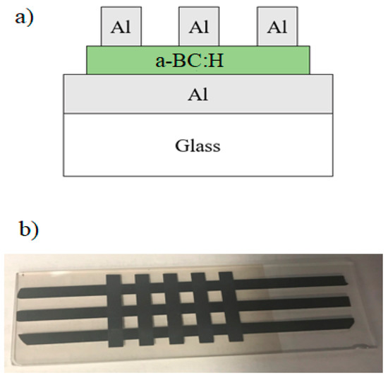
Figure 1.
(a) Schematic of the cross-sectional view of metal-insulator-metal (MIM) capacitor; (b) actual fabricated structure for the film deposited at 300 °C consisting of 15 MIM capacitor devices.
I-V characteristics were measured on MIM devices using a source meter (2450 Keithley, Moorpark, CA, USA). These data were used to extract resistivity (ρ) of the film. The capacitance of MIM devices was determined using HP 4275 multi-frequency LCR meter. The dielectric properties were investigated at low frequency of 100 kHz. The dielectric constant (k) of the film was calculated by
where C is the capacitance, d is the dielectric thickness, ε0 is the permittivity of free space, and A is area of capacitor. Thickness of the films was determined using Dektat 150 surface profilometer (Veeco, NY, USA). Optical transmission studies were performed using UV-Visible spectrophotometer (Cary 100, Varian, CA, USA).
k = (Cd)/(ε0A)
3. Results
3.1. XPS and REELS Analysis
The chemical states of the deposited film were investigated using XPS. The sample surface was etched using Ar ion gun of 1 kV for ~10 s prior to XPS. The high-resolution B 1s, C 1s, and O 1s spectra for the film deposited at RT are displayed in Figure 2. The B 1s region of the spectra is fitted with two peaks located at ~191 eV and 192.5 eV, corresponding to B–C–O and B–O bonds [21,22]. This suggests that B–C–O and B–O are primary interactions for boron in the film with B–C–O being dominant implying higher oxidation of boron atoms. The C 1s spectra exhibited three components centered at 284.8, 286.4, and 288 eV, respectively. The dominating component at 284.8 eV is attributed to sp2 C–C and C–H bonding in the films [23]. The shoulder peak at 286.4 eV is attributed to C–O–H, C–O–C, and peak at 288 eV is attributed to C=O [24]. While C–H, C–C is dominating component in C 1s spectra, the shoulder peak energies suggest that some C partially bonds with O in the films. The O 1s region of spectra is fitted with two peaks at 530.6 eV attributed to C–O–H and 532.5 eV attributed to O–B components in the films [24,25]. The C 1s and B 1s scans also verify this bonding configuration of the elements. Figure 3 shows the atomic content of C and B/C ratio obtained from XPS results. The films show carbon enriched a-BxCy:H composition. It can be observed that with increasing deposition temperature, the elemental C content of the film increases with a corresponding decrease in B/C ratio. C–C bonds dramatically increase with temperature due to structure modifications and atomic ordering. C elemental composition tends to increase due to dissociation process of remained hydrocarbides [26]. Such bond formations can be explained by means of Frenklash and Spear model [27], where the breaking of C–H bonds produces new C–C bonds.
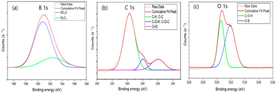
Figure 2.
XPS spectra of (a) B 1s, (b) C 1s, and (c) O 1s peaks for a-BC:H film deposited at room temperature (RT).
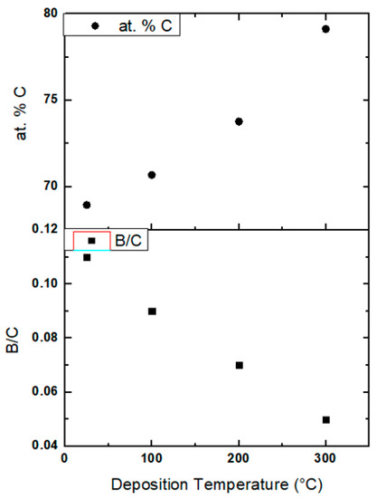
Figure 3.
Atomic percentage of C and corresponding B/C ratio as a function of deposition temperature.
A similar trend of increasing C content and corresponding decrease in B content with substrate temperature is reported for boron carbide films deposited using different techniques [26,28,29]. It was observed that the atomic oxygen concentration in the film was relatively high. We predict this could have originated due to lower density and post-growth atmospheric conditions.
As XPS cannot be used to detect hydrogen, REELS was used for hydrogen detection in boron carbide films. In order to avoid electron damage to the film surface, REELS measurements were performed with 1–2 keV electron beams. The angle of incidence of electron beam with respect to the surface normal was set to 60°. REELS spectra are shown in the Figure 4. The inset figure shows the complete REELS scan over 980–1010 eV kinetic energy for film deposited at 300 °C. The large peak at 1004 eV is due to elastically scattered electrons. Distinct shoulder peaks observed at 1003.5 eV are due to elastic scattering collisions with hydrogen atoms. The film deposited at 300 °C shows higher hydrogen content than other films. Hydrogen being the lowest atomic number element reduces the total mass density of the film and hence is known to reduce dielectric value of the film [17]. As the hydrogen concentration in the film is estimated to be less (<10%), it was difficult to quantify the atomic hydrogen content in these films.
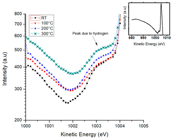
Figure 4.
Reflection electron energy loss spectroscopy (REELS) spectra for a-BC:H films deposited at different substrate temperatures showing peak at 1003.5 eV due to hydrogen atoms. Inset figure: complete REELS spectra from 980–1010 eV for film deposited at 300 °C.
3.2. Dielectric Constant
Figure 5 shows dielectric constant of a-BC:H thin films as a function of deposition temperature. The dielectric constant displayed decreasing trend with deposition temperature. The dielectric constant of pure boron carbide is reported between 4.8 and 8 [30]. The dielectric constant of a-BC:H films investigated in this study ranges from 6.5 to 3.5. The lowest dielectric value of 3.5 is achieved for the film deposited at 300 °C, which has maximum sp2 carbon content, lowest B/C ratio as seen from XPS results, and highest content of hydrogen (as revealed in REELS analysis). This reduction in dielectric value is associated with higher C content in the film, which reduces the film density. Lower film density enhances the free volume within the films, which is known to be an effective way of reducing dielectric constant of materials. Dielectric constant of a materials also reduces due to increased porosity owing to the presence of hydrogen content [31,32]. Higher C content and presence of hydrogen collectively contributed to lower dielectric values of the boron carbide films. The range of dielectric values observed in this study is consistent with that previously found in amorphous-hydrogen-doped boron carbide films synthesized using PECVD [17,33].
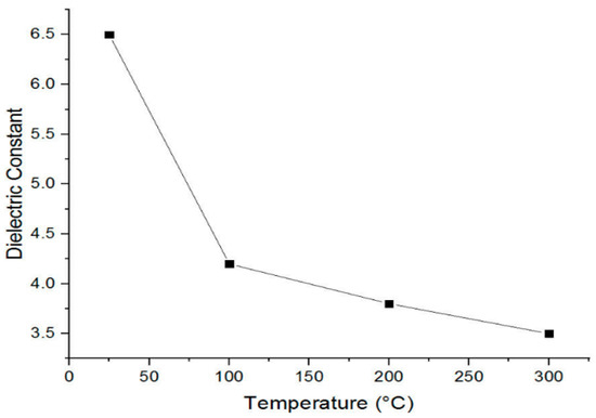
Figure 5.
Dielectric constant of a-BC:H films as a function of deposition temperature.
3.3. Resistivity
Resistivity trend of a-BC:H thin films as a function of deposition temperature is shown in Figure 6. The electrical resistivity for films varies in magnitude of 109 to 108 Ω·cm. The resistivity curve follows a decreasing trend with increase in deposition temperature. Pure boron carbide films grown in argon ambiance have been reported to exhibit resistivity value of the order of 109 Ω·cm at room temperature [34]. a-BC:H films investigated in this study displayed one order lower resistivity values at deposition temperature of 100–300 °C. With increasing substrate temperature, the C content incorporated in the film increased, with maximum content recorded for the film deposited at 300 °C, which results in reduced electrical resistivity. Changes in carbon hybridization due to increase in sp2 carbon content affect the number of free electrons in the films, which influences resistivity values [2]. Similar trends have been observed in boron carbide films where electrical resistivity decreased due to increasing C content in the film [35].
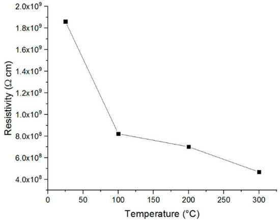
Figure 6.
Electrical resistivity of a-BC:H films as a function of deposition temperature.
3.4. Optical Transmission
Optical studies were performed on a-BC:H films deposited on glass slides. Figure 7 shows transmission for wavelength range of 200–800 nm. Transmission increases when films are deposited at higher temperature than RT. All films exhibit transmission between 75–82%, which is desired for applications in optical devices.
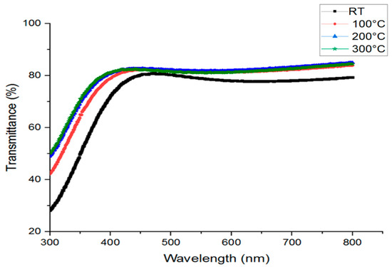
Figure 7.
Optical transmission studies of a-BC:H films.
3.5. Optical Bandgap
To calculate the optical bandgap, transmission (%T) data were used. The absorption coefficient (α) was calculated from the transmission data [36] using the following equation:
where OD is the optical density and t is the thickness of the deposited film. Optical bandgap (Eg) of the films deposited at different temperatures were estimated [36] using the following equation
where hν = photon energy, B = constant, and Eg is the optical band gap.
α = 2.303 * OD = (−2.303/t) log 10 (%T)
(αhν) (1/n) =B (hν − Eg)
Figure 8 shows the Tauc plot used to calculate Eg with n = 2. Typically, the n value is defined as 2 for amorphous films. The optical bandgap for the films was estimated by extrapolating linear regions of the curves to the energy axis. The measured bandgap values are listed in Table 1. The optical bandgap displayed a slight change from 2.25 eV to 2.6 eV as these films became more hydrogen-rich with increasing substrate temperature. A similar correlation between hydrogen concentration and Eg is reported in other low dielectric materials such as a-C:H [37], a-SiC:H [38], and a-Si:H [39]. The Eg values for a-BC:H films obtained in this study are comparable to bandgap values reported for amorphous hydrogenated boron carbide grown by PECVD [17].
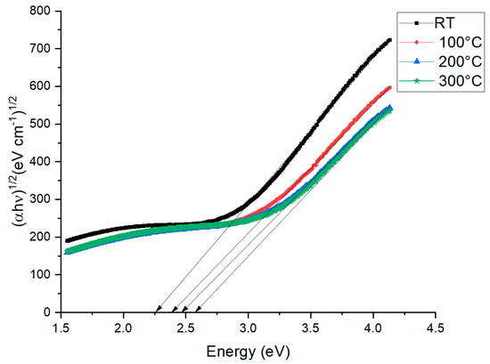
Figure 8.
Tauc plot of a-BC:H thin films deposited at different substrate temperatures.

Table 1.
Optical bandgap values obtained for a-BC:H films.
4. Conclusions
Advancing towards the search for new dielectric materials, a-BC:H films were grown using RF sputtering technique at different deposition temperatures. These films incorporate higher C content with increasing deposition temperature. An increase in C content resulted in a reduced B/C ratio in the films. These C-enriched films of a-BC:H exhibited lower dielectric constant of 3.5 and reduced electrical resistivity of 108 Ω·cm. By varying growth temperatures, we have established a wide range of optical properties such as optical transmission between 75 and 82% and Eg between 2.25 and 2.6 eV. These low-dielectric-constant and high-resistivity films of a-BC:H are promising as insulating materials for low-k dielectric applications. Further, their sensitive optical tunability at different substrate temperatures can be optimized for specific applications.
Author Contributions
Conceptualization, S.D.N. and K.B.S.; Investigation, S.D.N.; Methodology, S.D.N.; Supervision, K.B.S.; Writing—review & editing, A.K.S. All authors have read and agreed to the published version of the manuscript.
Funding
This research received no external funding.
Institutional Review Board Statement
Not applicable.
Informed Consent Statement
Not applicable.
Data Availability Statement
Data available on request.
Conflicts of Interest
The authors declare no conflict of interest.
References
- Grill, A.; Gates, S.M.; Ryan, T.E.; Nguyen, S.V.; Priyadarshini, D. Progress in the development and understanding of advanced low k and ultralow k dielectrics for very large-scale integrated interconnects—State of the art. Appl. Phys. Rev. 2014, 1, 011306. [Google Scholar] [CrossRef]
- Balakrishnarajan, M.M.; Pancharatna, P.D.; Hoffmann, R. Structure and bonding in boron carbide: The invincibility of imperfec-tions. New J. Chem. 2007, 31, 473–485. [Google Scholar] [CrossRef]
- Domnich, V.; Reynaud, S.; Haber, R.A.; Chhowalla, M. Boron Carbide: Structure, Properties, and Stability under Stress. J. Am. Ceram. Soc. 2011, 94, 3605–3628. [Google Scholar] [CrossRef]
- Reddy, K.M.; Liu, P.; Hirata, A.; Fujita, T.; Chen, M. Atomic structure of amorphous shear bands in boron carbide. Nat. Commun. 2013, 4, 2483. [Google Scholar] [CrossRef] [PubMed]
- Sezer, A.O.; Brand, J. Chemical vapor deposition of boron carbide. Mater. Sci. Eng. B 2001, 79, 191–202. [Google Scholar] [CrossRef]
- Thevenot, F. Boron carbide—A comprehensive review. J. Eur. Ceram. Soc. 1990, 6, 205–225. [Google Scholar] [CrossRef]
- Tu, R.; Hu, X.; Li, J.; Yang, M.; Li, Q.; Shi, J.; Li, H.; Ohmori, H.; Goto, T.; Zhang, S. Fabrication of (a-nc) boron carbide thin films via chemical vapor deposition using ortho-carborane. J. Asian Ceram. Soc. 2020, 8, 327–335. [Google Scholar] [CrossRef]
- Sasaki, S.; Takeda, M.; Yokoyama, K.; Miura, T.; Suzuki, T.; Suematsu, H.; Jiang, W.; Yatsui, K. Thermoelectric properties of bo-ron-carbide thin film and thin film based thermoelectric device fabricated by intense-pulsed ion beam evaporation. Sci. Technol. Adv. Mater. 2005, 6, 181. [Google Scholar] [CrossRef]
- Nordell, B.J.; Nguyen, T.D.; Keck, C.L.; Dhungana, S.; Caruso, A.N.; Lanford, W.A.; Gaskins, J.T.; Hopkins, P.E.; Merrill, D.R.; Johnson, D.C.; et al. Conquering the low-k death curve: Insulating boron carbide dielectrics with superior mechanical properties. Adv. Electron. Mater. 2016, 2, 1600073. [Google Scholar] [CrossRef]
- Annen, A.; Saß, M.; Beckmann, R.; Von Keudell, A.; Jacob, W. Structure of plasma-deposited amorphous hydrogenated bo-ron-carbon thin films. Thin Solid Films 1998, 312, 147–155. [Google Scholar] [CrossRef]
- Oliveira, J.; Conde, O. Deposition of boron carbide by laser CVD: A comparison with thermodynamic predictions. Thin Solid Films 1997, 307, 29–37. [Google Scholar] [CrossRef]
- Sun, J.; Ling, H.; Pan, W.; Xu, N.; Ying, Z.; Shen, W.; Wu, J. Chemical structure and micro-mechanical properties of ultra-thin films of boron carbide prepared by pulsed-laser deposition. Tribol. Lett. 2004, 17, 99–104. [Google Scholar] [CrossRef]
- Suematsu, H.; Kitajima, K.; Suzuki, T.; Jiang, W.; Yatsui, K.; Kurashima, K.; Bando, Y. Preparation of polycrystalline boron carbide thin films at room temperature by pulsed ion-beam evaporation. Appl. Phys. Lett. 2002, 80, 1153–1155. [Google Scholar] [CrossRef]
- Lee, K.; Lee, J.; Park, M.; Kim, J.; Lee, C.; Kim, C. Preparation of boron carbide thin films for HDD protecting layer. J. Magn. Magn. Mater. 2004, 272, 2197–2199. [Google Scholar] [CrossRef]
- Lousa, A.; Martínez, E.; Esteve, J.; Pascual, E. Effect of ion bombardment on the properties of B4C thin films deposited by RF sputtering. Thin Solid Films 1999, 355, 210–213. [Google Scholar] [CrossRef]
- Guruz, M.; Dravid, V.; Chung, Y. Synthesis and characterization of single and multilayer boron nitride and boron carbide thin films grown by magnetron sputtering of boron carbide. Thin Solid Films 2002, 414, 129–135. [Google Scholar] [CrossRef]
- Nordell, B.J.; Karki, S.; Nguyen, T.D.; Rulis, P.; Caruso, A.N.; Purohit, S.S.; Li, H.; King, S.W.; Dutta, D.; Gidley, D.W.; et al. The influence of hydrogen on the chemical, mechanical, optical/electronic, and electrical transport properties of amorphous hydrogenated boron carbide. J. Appl. Phys. 2015, 118, 035703. [Google Scholar] [CrossRef]
- Wang, X.; Xie, Y.; Tang, K.; Wang, C.; Yan, C. Redox chemistry of molybdenum trioxide for ultrafast hydrogen-ion storage. Angew. Chem. Int. Ed. 2018, 57, 11569–11573. [Google Scholar] [CrossRef] [PubMed]
- Ren, B.; Huang, J.; Yu, H.; Yang, W.; Wang, L.; Pan, Z.; Wang, L. Thermal stability of hydrogenated diamond films in nitrogen am-bience studied by reflection electron energy spectroscopy and X-ray photoelectron spectroscopy. Appl. Surf. Sci. 2016, 388, 565–570. [Google Scholar] [CrossRef]
- Shindo, D.; Sato, H.; Liedl, G.L. Determination of atomic hydrogen in hydrocarbons by means of the reflected electron energy loss spectroscopy and the X-ray photoelectron spectroscopy. J. Phys. Conf. Ser. 2016, 012005. [Google Scholar] [CrossRef]
- Liu, X.; Chen, X.; Singh, D.J.; Stern, R.A.; Wu, J.; Petitgirard, S.; Bina, C.R.; Jacobsen, S.D. Boron–oxygen complex yields n-type surface layer in semiconducting diamond. Proc. Natl. Acad. Sci. USA 2019, 116, 7703–7711. [Google Scholar] [CrossRef] [PubMed]
- Laidani, N.; Anderle, M.; Canteri, R.; Elia, L.; Luches, A.; Martino, M.; Micheli, V.; Speranza, M. Structural and compositional study of B–C–N films produced by laser ablation of B4C targets in N2 atmosphere. Appl. Surf. Sci. 2000, 157, 135–144. [Google Scholar] [CrossRef]
- Ago, H.; Kugler, T.; Cacialli, F.; Salaneck, W.R.; Shaffer, M.S.P.; Windle, A.H.; Friend, R.H. Work functions and surface functional groups of multiwall carbon nanotubes. J. Phys. Chem. B 1999, 103, 8116–8121. [Google Scholar] [CrossRef]
- Chowdhury, F.A.; Hossain, M.A.; Uchida, K.; Tamura, T.; Sugawa, K.; Mochida, T.; Otsuki, J.; Mohiuddin, T.; Boby, M.A.; Alam, M.S. Gra-phene oxide/carbon nanoparticle thin film based IR detector: Surface properties and device characterization. AIP Adv. 2015, 5, 107228. [Google Scholar] [CrossRef]
- Matsoso, B.J.; Ranganathan, K.; Mutuma, B.K.; Lerotholi, T.; Jones, G.; Coville, N.J. Synthesis and characterization of boron carbon oxynitride films with tunable composition using methane, boric acid and ammonia. New J. Chem. 2017, 41, 9497–9504. [Google Scholar] [CrossRef]
- Castillo, H.; Restrepo-Parra, E.; Velez, J.; De La Cruz, W. Substrate temperature influence on boron carbide coatings grown by the PLD technique. Surf. Coat. Technol. 2011, 205, 3607–3612. [Google Scholar] [CrossRef]
- Frenklach, M.; Spear, K.E. Growth mechanism of vapor-deposited diamond. J. Mater. Res. 1988, 3, 133–140. [Google Scholar] [CrossRef]
- Richter, F.; Herrmann, M.; Molnar, F.; Chudoba, T.; Schwarzer, N.; Keunecke, M.; Bewilogua, K.; Zhang, X.; Boyen, H.-G.; Ziemann, P. Substrate influence in Young’s modulus determination of thin films by indentation methods: Cubic boron nitride as an example. Surf. Coat. Technol. 2006, 201, 3577–3587. [Google Scholar] [CrossRef]
- Liu, Y.; Zhang, L.; Cheng, L.; Yang, W.; Xu, Y. Effect of deposition temperature on boron-doped carbon coatings deposited from a BCl3–C3H6–H2 mixture using low pressure chemical vapor deposition. Appl. Surf. Sci. 2009, 255, 8761–8768. [Google Scholar] [CrossRef]
- Prakash, A.; Sundaram, K.B. Studies on electrical properties of rf sputtered deposited boron carbon nitride thin films. ECS J. Solid State Sci. Technol. 2015, 4, N25–N29. [Google Scholar] [CrossRef]
- Shamiryan, D.; Abell, T.; Iacopi, F.; Maex, K. Low-k dielectric materials. Mater. Today 2004, 7, 34–39. [Google Scholar] [CrossRef]
- Chiang, C.-C.; Wu, Z.-C.; Wu, W.-H.; Chen, M.-C.; Ko, C.-C.; Chen, H.-P.; Jang, S.-M.; Yu, C.-H.; Liang, M.-S. Physical and barrier properties of plasma enhanced chemical vapor deposition α-SiC: N: H films. Jpn. J. Appl. Phys. 2003, 42, 4489. [Google Scholar] [CrossRef]
- Alimov, V.K.; Bogomolov, D.; Churaeva, M.; Gorodetsky, A.; Kanashenko, S.; Kanaev, A.; Rybakov, S.; Sharapov, V.M.; Zakharov, A.; Zalavutdinov, R.; et al. Characterization of a-B/C: H films deposited from different boron containing precursors. J. Nucl. Mater. 1992, 196, 670–675. [Google Scholar] [CrossRef]
- Lee, S.; Mazurowski, J.; Ramseyer, G.; Dowben, P.A. Characterization of boron carbide thin films fabricated by plasma enhanced chemical vapor deposition from boranes. J. Appl. Phys. 1992, 72, 4925–4933. [Google Scholar] [CrossRef]
- Wood, C.; Emin, D. Conduction mechanism in boron carbide. Phys. Rev. B 1984, 29, 4582–4587. [Google Scholar] [CrossRef]
- Tauc, J.; Grigorovici, R.; Vancu, A. Optical properties and electronic structure of amorphous germanium. Phys. Status Solidi (B) 1966, 15, 627–637. [Google Scholar] [CrossRef]
- Casiraghi, C.; Ferrari, A.C.; Robertson, J. Raman spectroscopy of hydrogenated amorphous carbons. Phys. Rev. B 2005, 72, 085401. [Google Scholar] [CrossRef]
- Tong, G.B.; Aspanut, Z.; Muhamad, M.R.; Rahman, S.A. Optical properties and crystallinity of hydrogenated nanocrystalline sili-con (nc-Si: H) thin films deposited by rf-PECVD. Vacuum 2012, 86, 1195–1202. [Google Scholar] [CrossRef]
- Basa, D.; Abbate, G.; Ambrosone, G.; Coscia, U.; Marino, A. Spectroscopic ellipsometry study of hydrogenated amorphous silicon carbon alloy films deposited by plasma enhanced chemical vapor deposition. J. Appl. Phys. 2010, 107, 023502. [Google Scholar] [CrossRef]


Publisher’s Note: MDPI stays neutral with regard to jurisdictional claims in published maps and institutional affiliations. |
© 2021 by the authors. Licensee MDPI, Basel, Switzerland. This article is an open access article distributed under the terms and conditions of the Creative Commons Attribution (CC BY) license (http://creativecommons.org/licenses/by/4.0/).