


Abstract
This paper proposes a novel 2-transformer (2-Trans)-based integrated on-board charger (OBC) and low-voltage DC/DC converter (LDC) system for electric vehicles. Conventional integrated OBC–LDC systems employing a three-winding transformer suffer from reduced light-load efficiency during standalone LDC operation because core losses dominate when designers size the transformer for high-power operation. In addition, concentrating multiple windings on a single magnetic core limits transformer design flexibility and causes complex magnetic coupling among the windings. To effectively reduce light-load losses and enhance transformer design freedom, this paper introduces a new integrated charging architecture that utilizes two independent transformers. The proposed system adopts a dual-active-bridge (DAB) converter for high-voltage battery charging and a phase-shift full-bridge (PSFB) converter for low-voltage battery charging. The system supports both simultaneous high- and low-voltage battery charging and standalone low-voltage battery operation, and a dual-phase-shift (DPS) control strategy enables independent and proper power flow control. Experimental results obtained from an 11 kW OBC and a 3 kW LDC prototype demonstrate up to a 33% reduction in light-load losses during standalone LDC operation and confirm the feasibility of improving power density through the proposed 2-Trans-based architecture.
1. Introduction
With the growing international concern over environmental issues and the strengthening of regulations related to carbon emissions and energy consumption, research on electric vehicles (EVs) based on environmentally friendly energy sources has accelerated worldwide [1,2,3,4]. In particular, continuous advancements in battery technology have steadily increased battery capacity, which in turn highlights the importance of power conversion systems capable of charging batteries rapidly and efficiently [5,6].
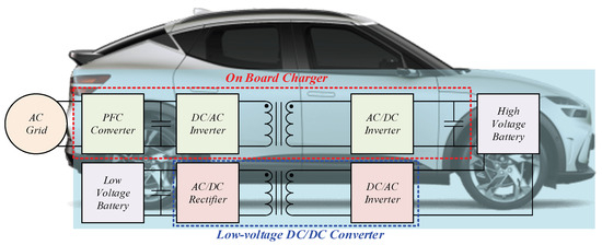
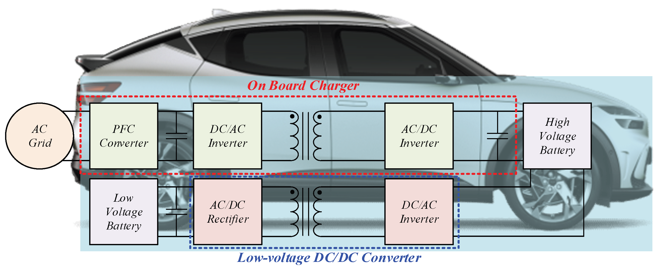
In general, the onboard power conversion system of an electric vehicle is configured as illustrated in Figure 1. The on-board charger (OBC) converts grid-side alternating current (AC) input into direct current (DC) to charge the high-voltage battery [7]. It typically consists of a power factor correction (PFC) circuit for improving the input power factor and performing AC/DC conversion, followed by an isolated DC/DC converter. The low-voltage DC/DC converter (LDC), on the other hand, receives power from the high-voltage battery and performs DC/DC conversion to supply the low-voltage battery, which powers various onboard electrical components such as lighting systems, air conditioning, and navigation units [8]. Providing a stable and efficient power supply from the LDC is not only essential for these basic functions but also serves as a critical infrastructure for advanced system-level functionalities. For instance, recent studies highlight the necessity of reliable power for health assessment frameworks in lithium-ion battery cyber defense systems [9] and for maintaining the stability of nonlinear vehicle platoons against external perturbations [10].
Figure 1.
Schematic diagram of OBC and LDC architecture.
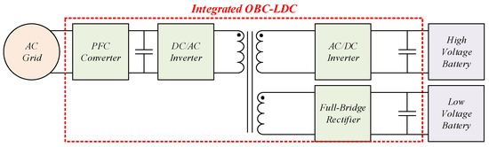
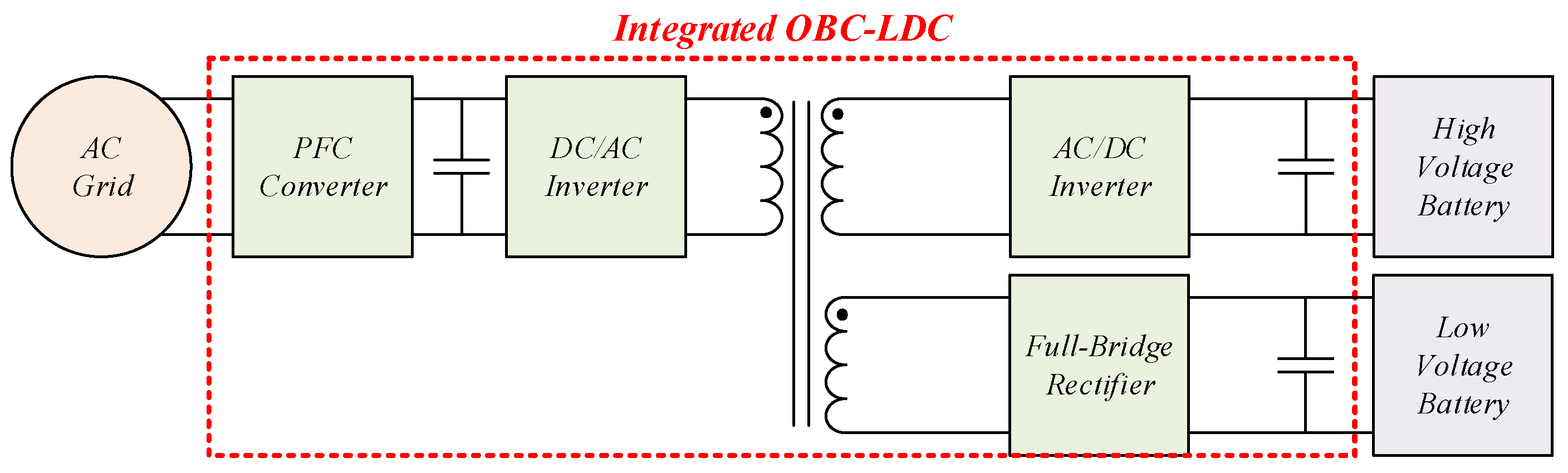
Since both the OBC and LDC significantly affect the charging speed and driving range of electric vehicles and are required to be installed within limited onboard space, high power density and high efficiency are essential design requirements. Accordingly, as shown in Figure 2, an integrated OBC–LDC system that performs both OBC and LDC power conversion functions within a single system has been introduced [11,12]. The integrated OBC–LDC system can reduce the number of required circuit components and magnetic elements, thereby contributing to effective reductions in system weight and volume [13,14]. Based on the power flow, the operating modes of the integrated OBC-LDC can be broadly classified into the following two modes:
Figure 2.
Schematic diagram of integrated OBC-LDC System.
- Simultaneous OBC–LDC operation mode: This mode occurs when the vehicle is stationary and connected to the grid, during which the high-voltage battery is charged while power is simultaneously supplied to low-voltage loads.
- Standalone LDC operation mode: This mode corresponds to the driving condition of the vehicle. Considering the state of charge (SoC) characteristics of a typical low-voltage battery, the LDC predominantly operates in the light-load region, generally between 10% and 50% of the rated load.
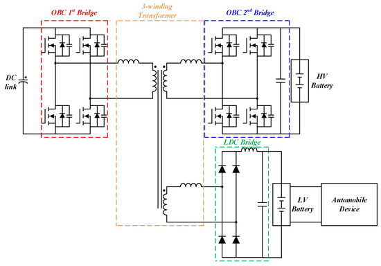
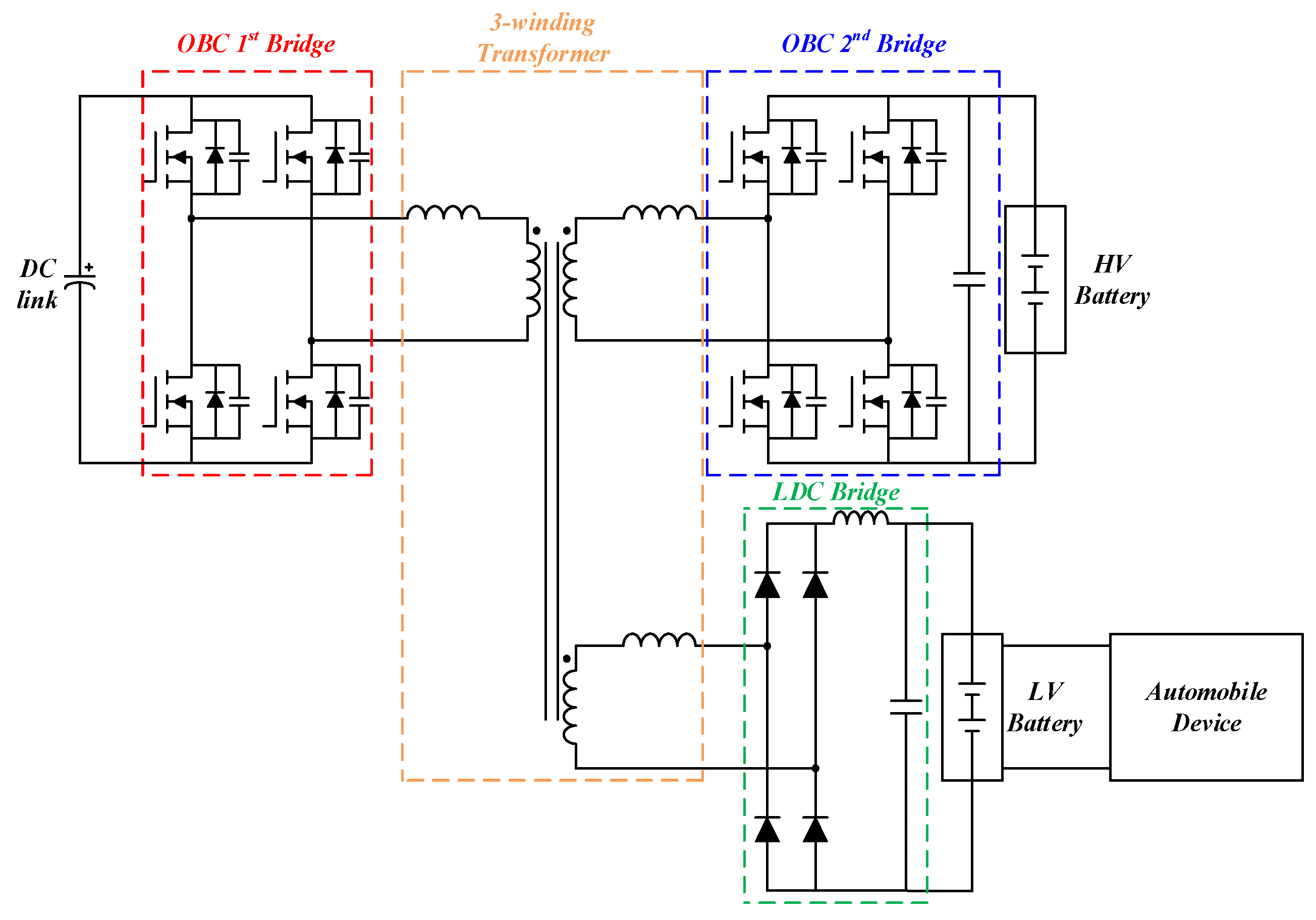
In conventional integrated OBC–LDC systems, as shown in Figure 3, power conversion for both the OBC and LDC is simultaneously achieved using a single three-winding transformer [15,16]. In this configuration, all three windings are wound on a single magnetic core, resulting in complex magnetic coupling characteristics. Consequently, the difficulty of transformer design and accurate modeling is significantly increased. Various design requirements, including turn ratio selection, winding arrangement, and leakage inductance matching, must be simultaneously satisfied within a limited window area [17,18]. As a result, there exist inherent limitations in transformer optimization, leading to reduced design flexibility. Moreover, to accommodate the combined power ratings, a magnetic core with a relatively large volume is required. Since transformer core loss generally increases in proportion to core volume, this configuration inherently results in increased losses. In the light-load region of standalone LDC operation, core loss becomes the dominant component of the total losses, significantly degrading efficiency.
Figure 3.
Topology diagram of integrated OBC–LDC system based on 3-winding transformer.
To mitigate these losses, existing technical approaches have focused on control strategies such as pulse frequency modulation (PFM), burst mode operation, and phase-shift optimization [19,20]. While these methods effectively reduce switching losses, they often result in increased output voltage ripple and complicate EMI filter designs. Furthermore, they do not resolve the fundamental issue of core loss inherent in large integrated transformers. Recent literature has explored various multi-port integrated charging solutions [21]; however, many of these systems encounter challenges related to cross-regulation between ports and increased control complexity, which can limit their robustness in real-world implementations.
In this paper, to address the aforementioned issues, a novel integrated OBC–LDC based on a 2-transformer (2-Trans) architecture is proposed, in which independent transformers are applied to the OBC and LDC, respectively. The proposed architecture integrates the OBC secondary-side and LDC primary-side inverters, preserving the component-reduction advantages of conventional systems while enabling independent optimization of both transformers through complete physical decoupling. This structural modularity effectively reduces core loss during standalone LDC operation and enhances scalability to higher power levels. By distributing heat sources, it also simplifies thermal management and improves long-term reliability by lowering voltage and current stresses on individual components.
To validate the proposed approach, a 14 kW prototype was developed. Experimental results demonstrate a maximum loss reduction of 33% under light-load standalone LDC operation. Furthermore, both the standalone LDC and simultaneous OBC–LDC operation modes were experimentally verified, confirming the practical feasibility and operational viability of the proposed system for real-world EV platforms.
2. Proposed Integrated Charging System
2.1. Analysis of Proposed Integrated Circuit
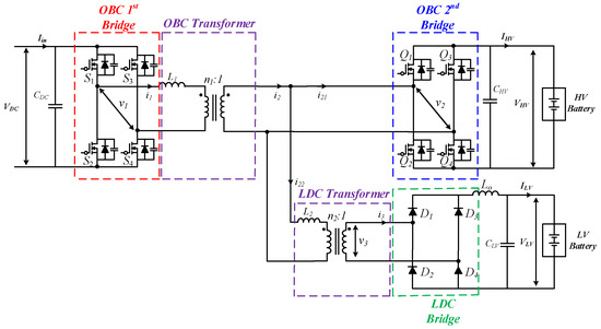
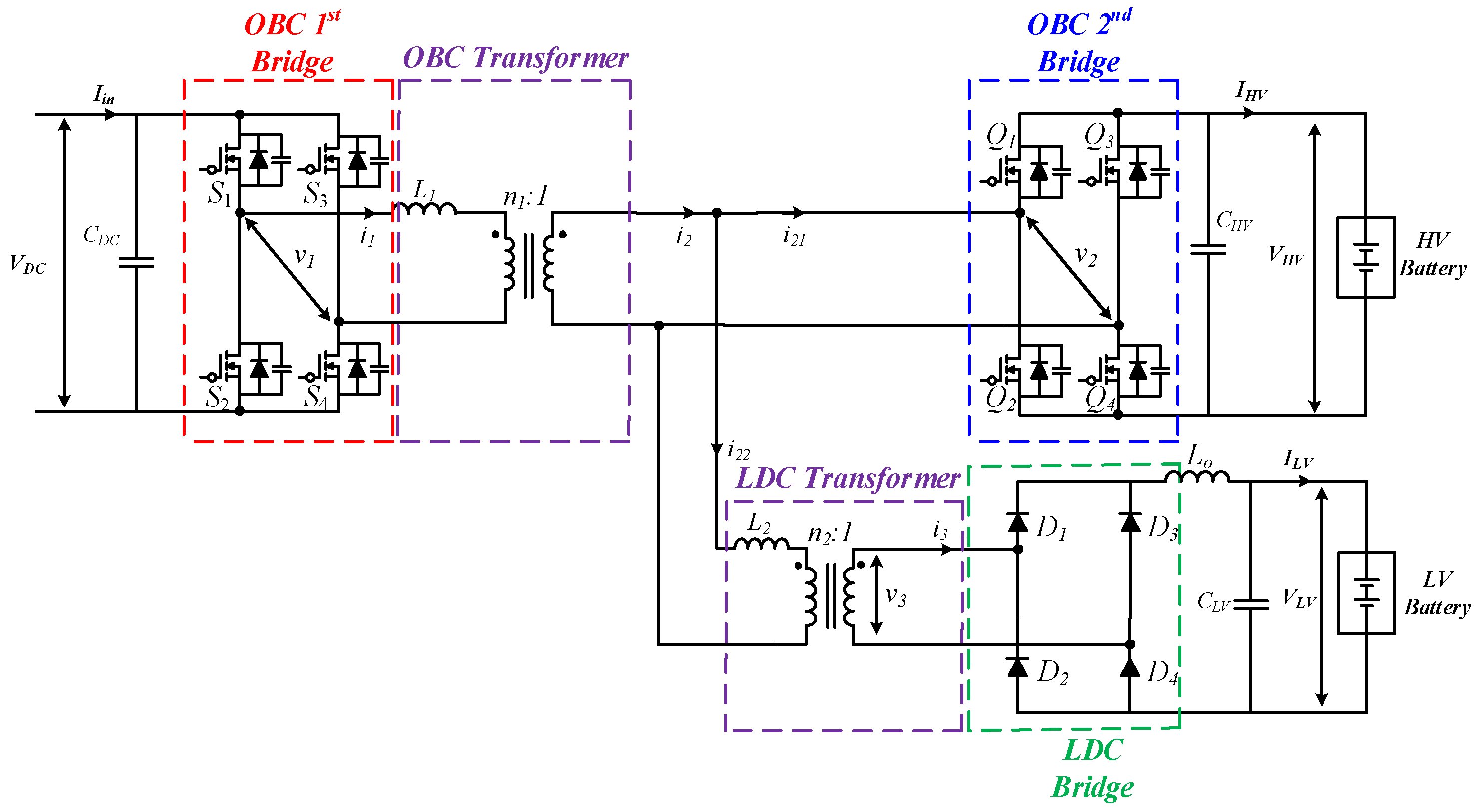
The circuit configuration of the proposed integrated OBC–LDC is shown in Figure 4. The proposed system adopts a 2-Trans architecture, in which two transformers are independently employed to handle power transfer for the OBC and the LDC, respectively.
Figure 4.
Topology circuit diagram of proposed integrated OBC–LDC.
The OBC transformer is implemented as a high-frequency (HF) transformer that provides galvanic isolation between ports, and it is modeled using an equivalent leakage inductance and turn ratio of . Similarly, the LDC transformer is also implemented as an HF transformer and is represented by an equivalent leakage inductance and turn ratio of . The magnetizing current of the transformers can be neglected because the magnetizing inductance is significantly larger than the leakage inductance. A DC-link capacitor is placed at the input of the OBC bridge, across which the output voltage of the PFC stage, denoted as , is applied. This voltage serves as the input DC voltage of the bridge. In this paper, the output voltage of the PFC stage is assumed to be regulated to a constant value , and the detailed operation of the PFC stage is not considered. The voltages and represent the high-voltage (HV) and low-voltage (LV) battery voltages, respectively, while and denote the corresponding output DCs. The bridge consists of four Mosfet, . The bridge output voltage and the current flowing through the are denoted as and , respectively. The bridge is composed of four Mosfet , and the corresponding bridge voltage is denoted as . The secondary side current of the OBC transformer, , is divided into two paths: the current , which is delivered to the HV battery through the bridge, and the current , which flows through the of the LDC transformer. This structure enables physical separation of the power transfer paths for the OBC and the LDC, allowing independent design and control of each transformer. The rectifier bridge on the LDC side is composed of four diodes, , and the corresponding output voltage is denoted as . The output filter capacitor of the OBC is represented by , while the output filter inductor and capacitor of the LDC are denoted as and , respectively.
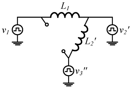
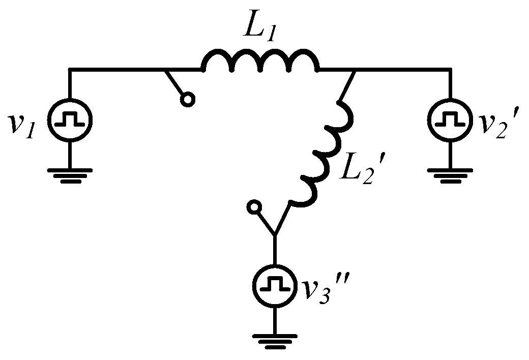
The system equivalent circuit represented by the bridge voltages and the leakage inductances of the 2-Trans structure can be expressed as a delta -type equivalent circuit, as shown in Figure 5. The winding resistances of the transformers are neglected, and the circuit is referred to the primary side of the OBC transformer. The equivalent parameters are given as follows:
Figure 5.
-type equivalent model of 2-Trans.
In contrast to the conventional 3-winding transformer, the 2-Trans structure inherently eliminates the magnetically coupled inductance between the OBC primary-side bridge and the LDC bridge. This power path decoupling removes unnecessary energy interaction with the OBC side during LDC standalone operation, effectively suppressing unintended circulating power.
To analyze the power transfer characteristics of the 2-Trans system, an equivalent circuit transformation is performed as shown in Figure 6. Figure 6a presents the equivalent representation of the PSFB converter referred to the primary side of the LDC transformer. The corresponding equivalent parameters are given as follows:
Figure 6.
Equivalent circuit model of 2-Trans system. (a) Only LDC Trans conversion. (b) 2-Trans conversion.
Figure 6b shows the equivalent circuit obtained by referring all parameters to the primary side of the OBC transformer. The corresponding equivalent parameters are defined as follows:
The input power is distributed into the HV battery side power and the LV battery side power . The is transferred to the HV battery side through the based on the operating principle of the DAB converter. Meanwhile, the LV battery power is delivered according to the switching operation of the bridge, following the power transfer mechanism of PSFB converter. Equation (7) represents the power relationship between ports.
2.2. Operation Mode
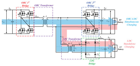
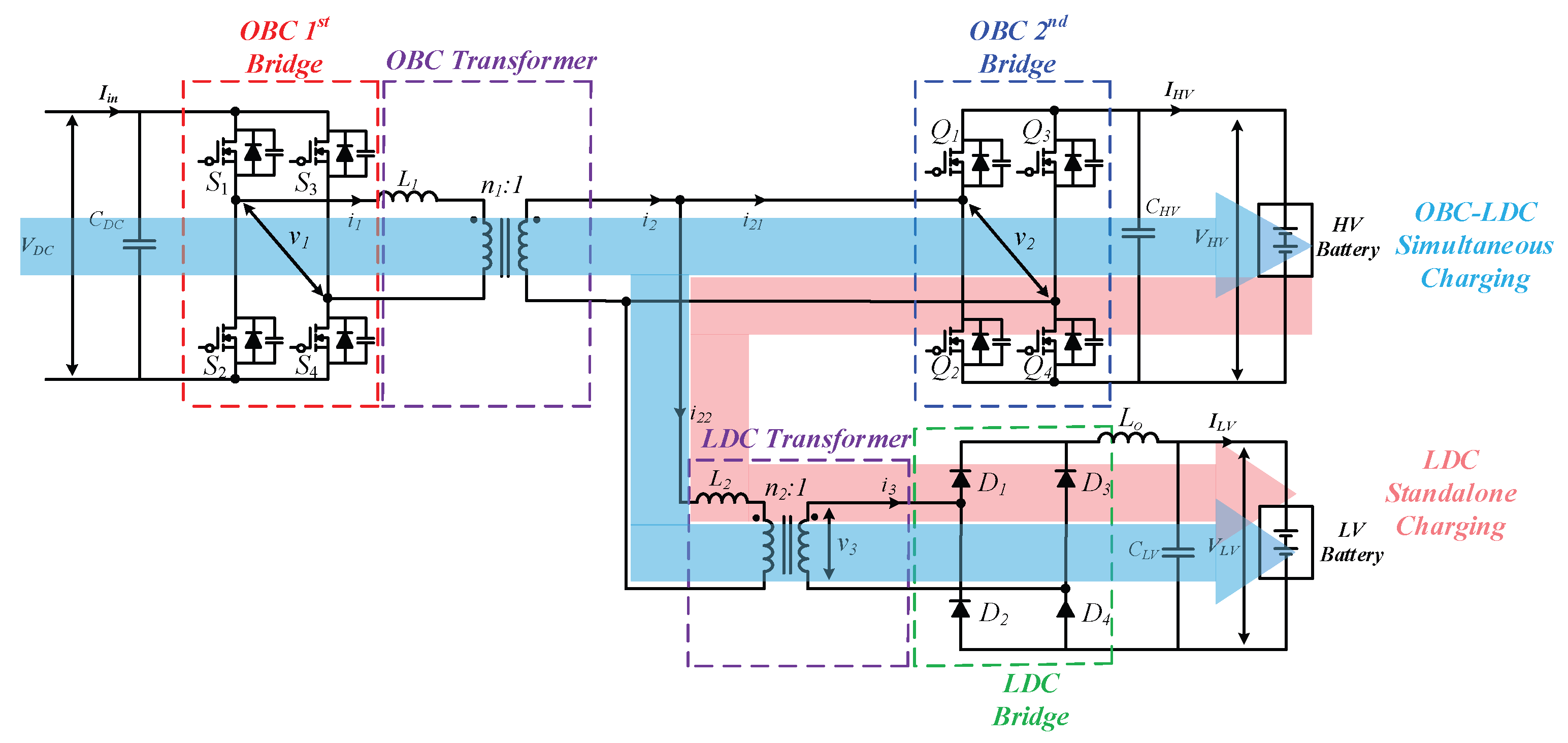
Since the integrated charging system integrates both OBC and LDC functions, various operating modes can be defined according to the power flow direction and the configuration of the input and output ports. The operating modes of the proposed integrated OBC-LDC are illustrated in Figure 7.
Figure 7.
Operation mode of the proposed integrated OBC–LDC.
In the simultaneous OBC–LDC charging mode, the system is connected to the grid and delivers power to both the HV and LV batteries simultaneously. The HV battery charging is achieved through the OBC bridge and transformer, following the power transfer principle of a DAB converter. Meanwhile, the LV battery charging is performed through the LDC transformer, where power is transferred according to the switching operation of the OBC secondary-side bridge, following the operating principle of a PSFB converter.
In the LDC standalone charging mode, the system is disconnected from the grid, and the LV battery is charged using the energy supplied from the HV battery. In this mode, power transfer is also governed by the switching operation of the OBC secondary-side bridge, operating in the same principle as a PSFB converter. However, in conventional structures, unintended power can be magnetically induced through the OBC transformer, which may lead to excessive voltage buildup across the DC-link capacitor and consequently degrade system reliability. To address this issue, this paper proposes a control strategy in which the switching operation of the OBC primary-side bridge is regulated during LDC standalone operation, limiting the power delivered to the grid side to less than . This study primarily focuses on the LDC standalone operation mode, which accounts for the largest portion of the battery charging profile in EVs. Nevertheless, since the simultaneous operation mode is also an essential charging process, the feasibility of the proposed method is additionally validated through experimental results.
2.3. Basic Principle Analysis and Control Method
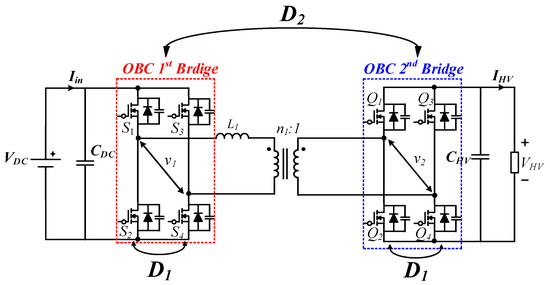
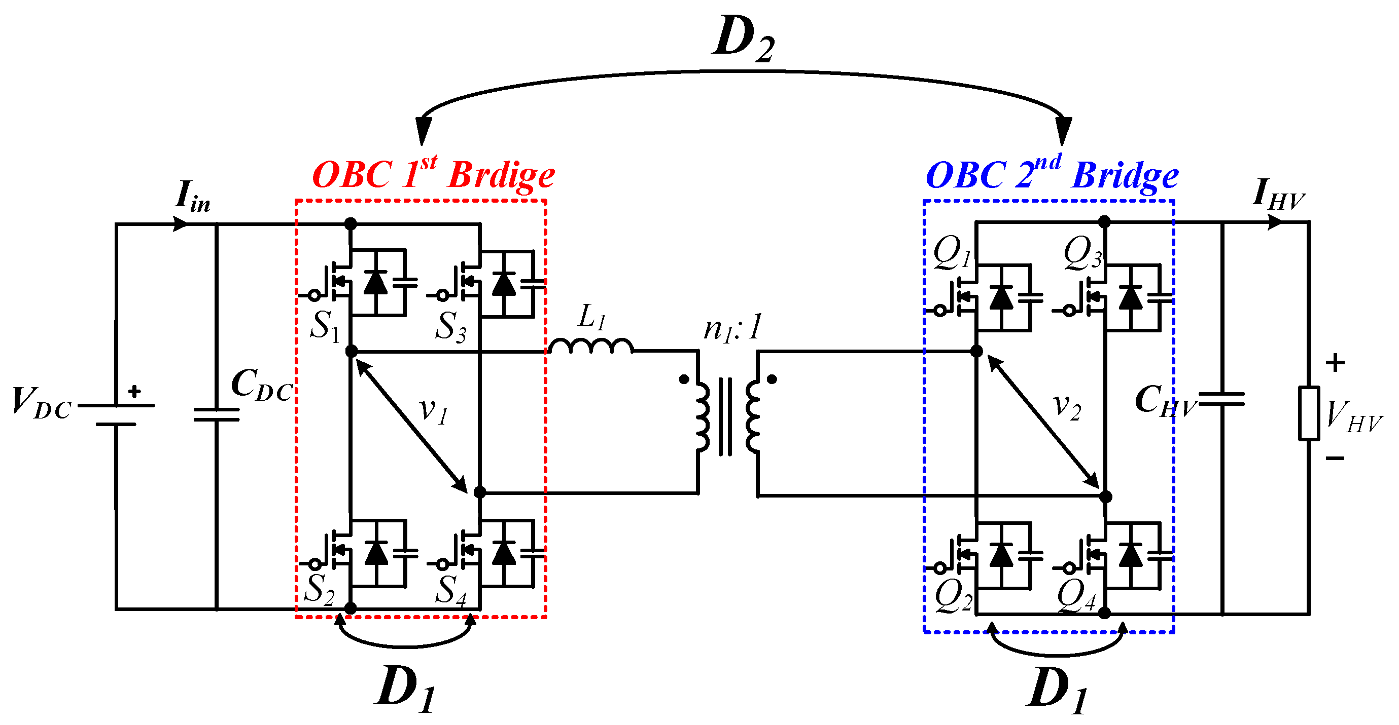
The proposed converter in this paper is capable of simultaneously driving up to two output ports from a single input power source. Therefore, at least two degrees of freedom (DOFs) are required to independently regulate the power of each output. To satisfy this requirement, a dual-phase-shift (DPS) control scheme is adopted to control the power of the OBC and LDC. In general, the DPS control method contributes to extending the ZVS operating region and reducing circulating power. In addition, since one control variable can be allocated to the power regulation of the LDC, the DPS control scheme is well suited to the proposed converter topology. To analyze the power transfer characteristics of the proposed control strategy, an understanding of the fundamental operating principles of the DAB and PSFB converters, as described by (7), is required. As illustrated in Figure 8, the DPS control scheme employs two control variables: the external phase shift () between the bridges and the internal phase shift () within each bridge [19].
Figure 8.
Control variables of DPS control method.
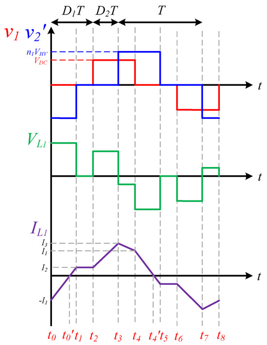
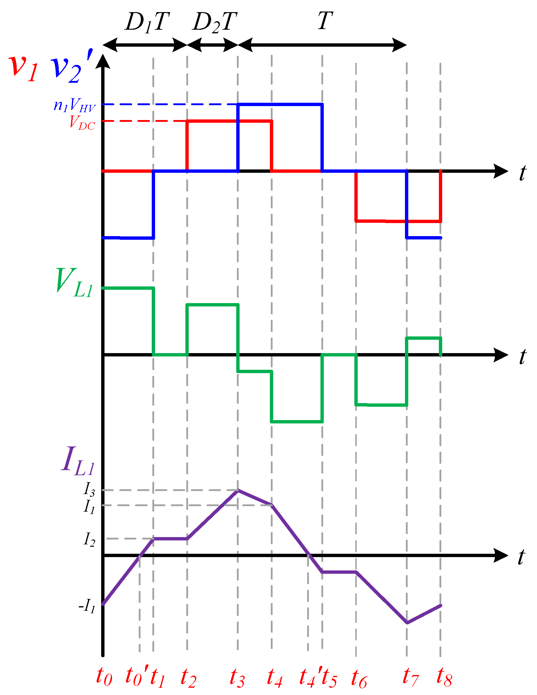
The symbols shown in Figure 8 are the same as those defined in Figure 4. The key waveforms under DPS control are illustrated in Figure 9. The waveforms correspond to boost mode with operating conditions of , .
Figure 9.
Main waveforms of DAB converter under DPS control.
denotes the turns ratio of the OBC transformer, represents the voltage across the leakage inductance , and denotes the leakage inductance current. Owing to the half-cycle symmetry of the waveforms, the analysis is carried out over half of the switching period, . is given as follows:
The inductor current is given as follows:
Based on the voltage–second balance of the inductor and the voltage–current relationship, the inductor current values at each switching instant can be expressed as follows:
The values of are summarized in Table 1.
Table 1.
Inductor current.
The average value of the inductor current is given as follows:
The input power can be expressed as follows:
The output current waveform is determined as follows according to the switching states of the bridge.
The above analysis focuses on the , operating region among the operating regions of the DPS control scheme. This region covers the majority of practical operating conditions under which the system operates normally in the presence of input–output voltage variations and load fluctuations, and it corresponds to the operating region where power control is actually performed in real system operation. This is because, during standalone LDC operation, power transfer is achieved solely through the control of , while during simultaneous OBC–LDC operation, the system controls below 0.5 in order to maximize the power transfer capability of the OBC. In addition, this operating region enables stable power transfer and satisfies the ZVS condition while suppressing excessive circulating current [20]. As a result, it has practical significance from the perspectives of system efficiency and reliability. Therefore, this paper selects this operating region as the representative operating region and analyzes the power transfer characteristics accordingly.
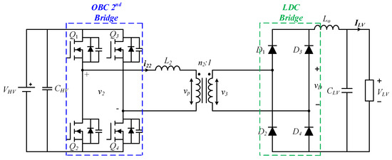
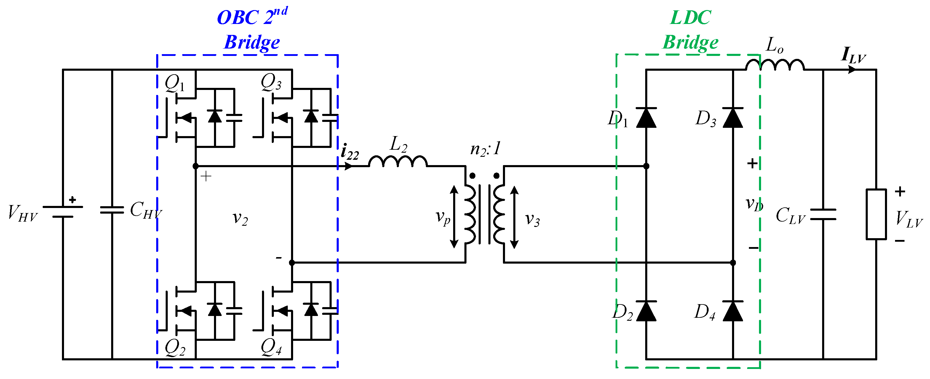
To derive the power delivered to the LV battery, the operation of the PSFB converter must be analyzed. The PSFB operation of the proposed system is illustrated in Figure 10.
Figure 10.
PSFB circuit diagram.
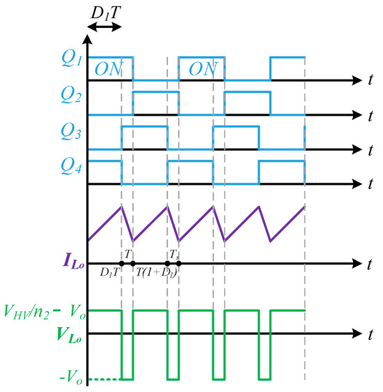
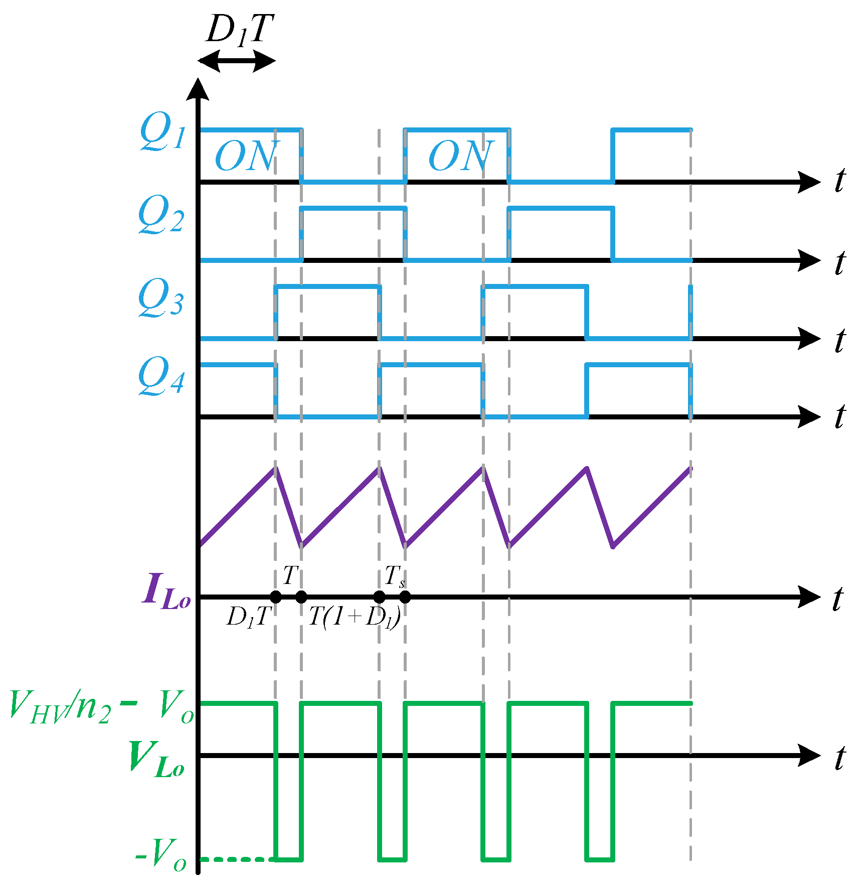
In the PSFB converter, the secondary-side diode bridge cannot be actively controlled, resulting in a commutation delay that depends on the load current magnitude. In addition, the presence of leakage inductance causes the current transition to occur gradually rather than instantaneously. As a result, the effective power transfer interval during each switching period is reduced, leading to duty loss, and the actual transferred power becomes lower than that predicted by the ideal commanded duty ratio [21]. Therefore, to accurately analyze the power transfer characteristics of the PSFB converter, the concept of an effective duty ratio, rather than the commanded duty ratio, should be employed. Figure 11 illustrates the voltage and current waveforms of the output filter inductor under switching operation, and Table 2 summarizes the output inductor voltage for each operating interval.
Figure 11.
Output filter inductor voltage and current waveforms.
Table 2.
Output filter inductor voltage.
By applying the voltage–second balance condition of the inductor, the voltage gain is obtained as follows.
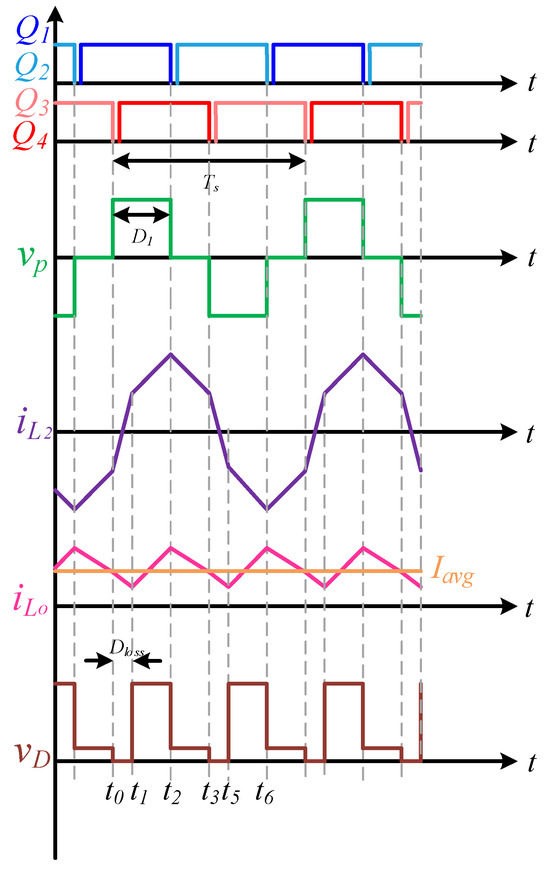
To derive the LV battery power , the key waveforms are illustrated in Figure 12.
Figure 12.
Key waveforms of PSFB.
The transferred power can be expressed as (21) by calculating it from the current of the leakage in each operating interval.
3. Transformer Design
3.1. OBC Transformer
This subsection describes the design of the OBC transformer used in the proposed 2-Trans integrated OBC–LDC. The transformer is designed for a DAB converter operating under DPS control, and its key parameters, including the turns ratio and leakage inductance, are carefully selected to achieve ZVS operation and reduced circulating current. The input and output rated parameters of the designed system are given in Table 3.
Table 3.
Input and output rated parameters.
The light-load experimental condition for the standalone LDC operation is set to 300 W and 450 W in order to reflect a representative auxiliary load level encountered during actual electric vehicle operation and charging. Previous studies report that, during OBC operation or vehicle driving, the low-voltage system continuously supplies power on the order of several hundred watts to auxiliary loads such as the battery management system, instrument cluster, communication modules, sensors, and control units. In [8], the authors report that the continuous power provided by the auxiliary power module (APM) during OBC operation generally remains below 400 W, and they also indicate that the APM operates for extended periods in the light-load region during driving mode. This observation suggests that the light-load efficiency of the standalone LDC operation plays a critical role in overall energy consumption. In addition, [13] evaluates the performance of an integrated charging system by selecting 430–450 W as the representative power demand of the low-voltage port under experimental conditions. This choice supports the view that a few-hundred-watt load level constitutes a reasonable and representative light-load operating region for practical electric vehicle applications. Based on these literature findings, 300 W and 450 W correspond to approximately 10% and 15% of the rated 3 kW LDC power, respectively, and can be regarded as representative light-load operating points that reflect continuous auxiliary power demand in real electric vehicle operation. Therefore, this paper selects 300 W and 450 W as light-load experimental conditions to clearly verify the loss reduction capability of the proposed 2-Trans architecture in the operating region where transformer core loss becomes dominant.
When the input and output voltage ranges are fixed, designers can easily select the transformer turns ratio such that the equivalent voltage ratio becomes unity. However, the proposed system operates over a wide and variable voltage range. Therefore, when designing the transformer turns ratio, it is essential to consider the characteristics of DAB converter in order to maximize the ZVS operating region. According to (16), the transferable power decreases as the leakage inductance increases. Consequently, a smaller leakage inductance is favorable for delivering higher power. However, excessively reducing the leakage inductance increases control sensitivity and can deteriorate ZVS performance due to rapid changes in inductor current. Although the proposed system operates with variable input and output voltages, these voltages vary within the same range. Accordingly, this study selects a transformer turns ratio of unity, which provides the widest ZVS operating region across all operating conditions. For the DAB converter, designers can determine the minimum value of leakage inductance by considering the ZVS achievement condition. To satisfy ZVS, the current flowing through the leakage inductance during the dead-time interval must fully charge and discharge the parasitic capacitances of the switches through resonant action. Therefore, when the parasitic output capacitance of the switch is denoted as , the minimum required leakage inductance can be expressed as follows:
When designing the OBC transformer, minimizing core loss is desirable if the efficiency of the standalone LDC charging mode alone is considered, since core loss occurs almost independently of the load condition. However, the proposed system must handle the rated power of 11 kW during simultaneous operation, and a design based solely on core loss minimization becomes insufficient. Therefore, the transformer design requires appropriate selection of the number of turns, core material, and winding configuration by considering the trade-off between copper loss and core loss. The expressions for core loss and copper loss can be evaluated using the following equations.
In (23) and (24), denotes the RMS current flowing through the winding, represents the electrical resistivity of the winding conductor, is the total length of the winding, denotes the cross-sectional area of the winding, represents the core volume, and denotes the Steinmetz coefficient determined by the magnetic core material. The OBC transformer is designed using a PQ6358 core made of PC95 ferrite and manufactured by TDK Corporation in Tokyo, Japan. The PC95 ferrite exhibits high permeability and excellent temperature stability, and it shows relatively small loss variation with changes in magnetic flux density under high-frequency operation. These characteristics make the PC95 material well suited for high-frequency transformer design in OBC applications. In addition, the PQ6358 core features a large effective cross-sectional area and a short magnetic path length, which effectively reduces the magnetic flux density under the same input conditions and thus provides advantages in minimizing core loss.
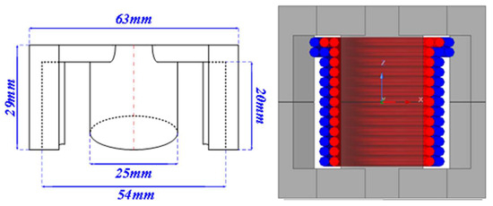
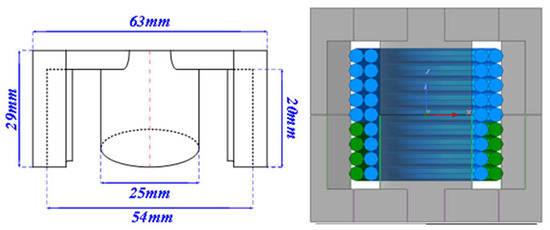
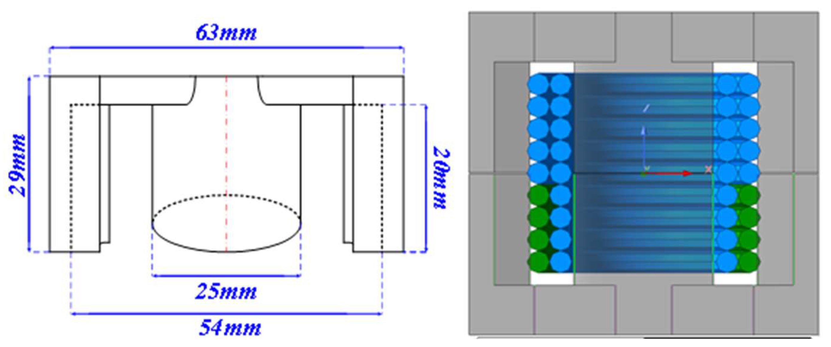
Table 4 summarizes the designed transformer parameters. In addition, Figure 13 illustrates the selected core size and the transformer design obtained through Ansys Maxwell FEM simulations. The software version used in this study is Ansys Electronics Desktop 2021 R1.
Table 4.
OBC Transformer parameter based on the FEM simulation.
Figure 13.
OBC transformer core size and Ansys Maxwell simulation design.
3.2. LDC Transformer
For the LDC, the HV battery serves as the input voltage source, and the converter operates with a fixed output voltage of 45 V. Under these specifications, the transformer turns ratio can be determined based on the voltage gain relationship of the PSFB converter, as expressed below.
Similarly to the DAB converter, the PSFB converter ZVS through the charging and discharging of the switches’ parasitic capacitances during the dead-time interval. Therefore, the following condition must be satisfied to ensure ZVS operation.
The selection of the winding configuration and core can be guided by (23) and (24). Considering the low-voltage and high-current characteristics, the secondary winding of the LDC transformer is implemented using a two-parallel winding structure.
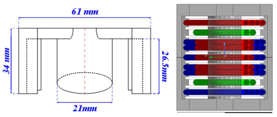
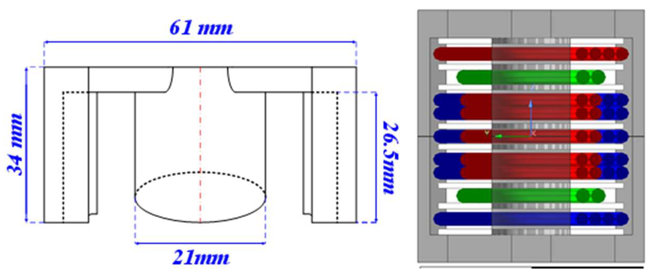
Table 5 summarizes the designed transformer parameters. In addition, Figure 14 illustrates the selected core size and the transformer design obtained through Ansys Maxwell FEM simulations. The LDC transformer also employs PC95 ferrite material, consistent with the OBC transformer design. According to (25), the transformer turns ratio is selected as 14:2. To improve efficiency during simultaneous operation, a winding thickness of 4 mm is applied to reduce winding resistance. To accommodate the increased winding thickness, the LDC transformer adopts the same PQ6358 core as the OBC transformer.
Table 5.
LDC Transformer parameter based on the FEM simulation.
Figure 14.
LDC transformer core size and Ansys Maxwell simulation design.
4. Experimental Results
In this section, based on the analysis in Section 2 and Section 3, the proposed system prototype is designed. The proposed converter operates at a switching frequency of 100 kHz and is capable of simultaneously delivering 11 kW and 3 kW to the HV and LV batteries, respectively. In addition, experimental validation of a conventional 3-winding transformer-based system was also conducted for comparative analysis with the proposed system.
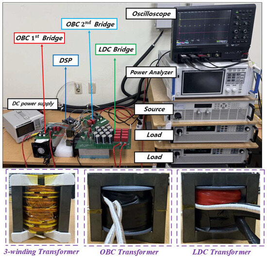
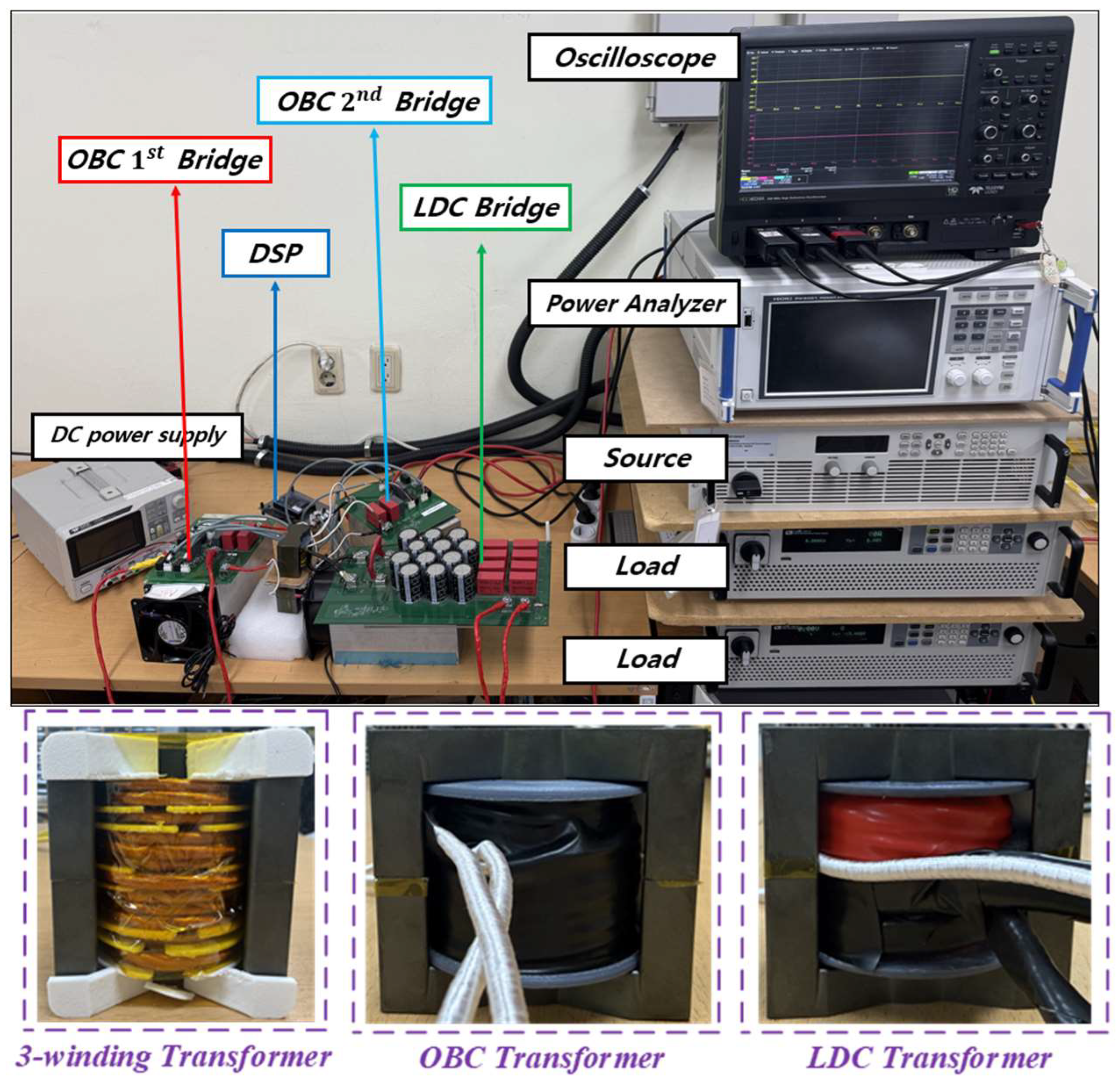
The parameters and design of the 3-winding transformer are presented in Figure 15 and Table 6. For the OBC bridge, the AIMZH120R030M1T Mosfet manufactured by Infineon Technologies AG in Neubiberg, Germany, was adopted. While the STPS60SM200C diode manufactured by STMicroelectronics in Geneva, Switzerland, was used for the LDC bridge. The control board was designed based on the TMS320F28335 microprocessor from Texas Instruments, and PWM signals were generated according to the control variables and . The transformer was implemented using a PC95 ferrite core based on the design presented in Section 3, and litz wire was employed for the windings. Figure 16 shows the prototype and the specifications of the proposed converter prototype are presented in Table 7.
Figure 15.
3-winding transformer core size and Ansys Maxwell simulation design.
Table 6.
3-winding Transformer parameter.
Figure 16.
Experimental prototype.
Table 7.
Key parameters of the prototype system.
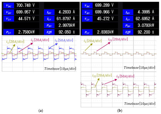
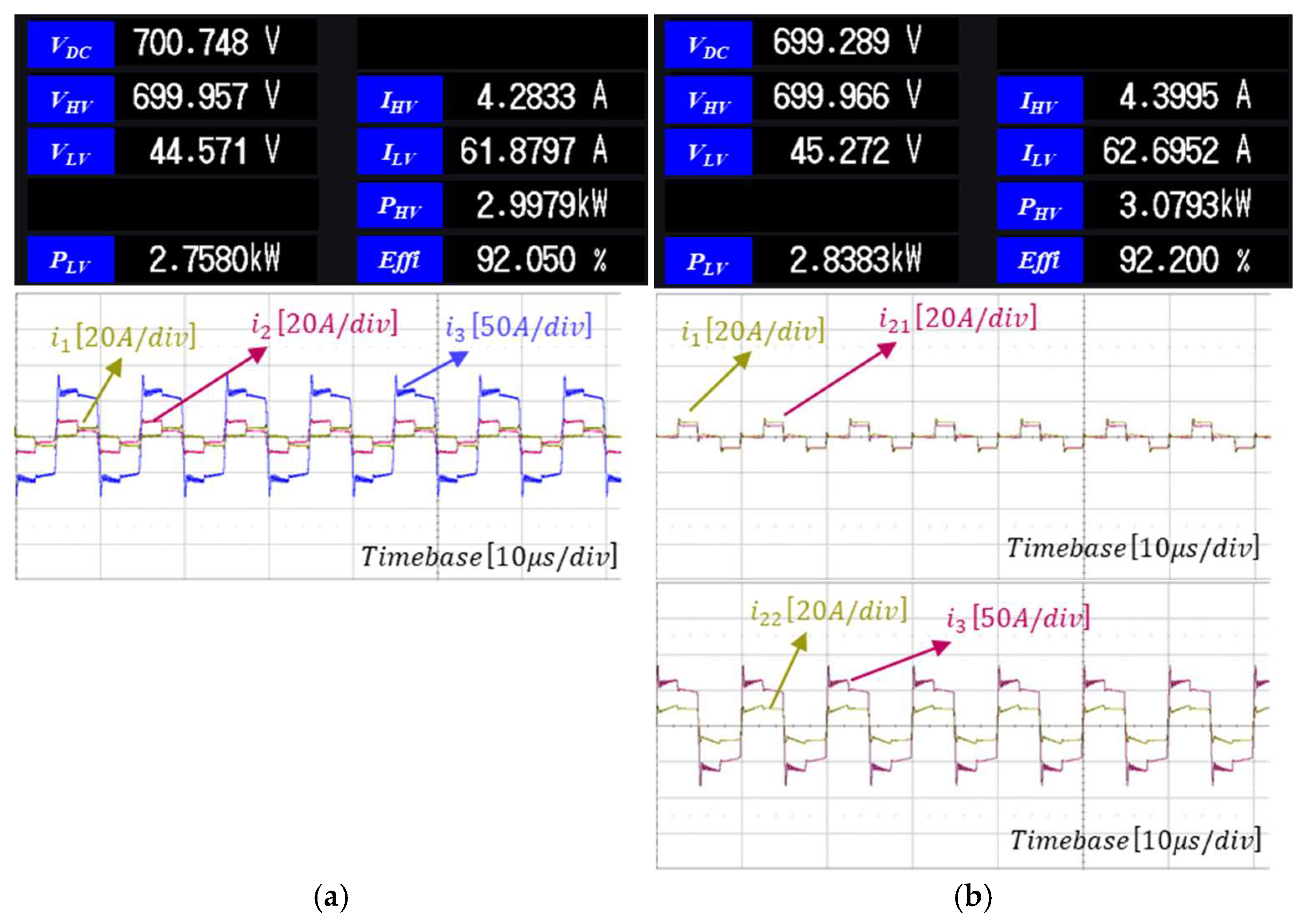
Figure 17 presents the experimental results under full-load conditions during standalone LDC operation. Under this operating mode, the low-voltage and high-current characteristics make the copper loss of the LDC transformer and the diode loss the dominant loss components. In addition, the system controls the switches of the OBC primary-side bridge to regulate the DC-link capacitor voltage, while maintaining the DC-link voltage and power at approximately 700 V and 0.5 W, respectively. In the experimental results of the three-winding transformer-based system shown in Figure 17a, all switches achieve ZVS, and the system reaches an efficiency of 92.05%. In contrast, the proposed system shown in Figure 17b maintains ZVS operation for all switches while improving the efficiency to 92.2%. This improvement results from securing a sufficiently large cross-sectional area of the LDC transformer core, which enables stable magnetic flux density control and effectively reduces copper loss.
Figure 17.
LDC standalone operation full-load (3 kW) experimental results (a) 3-winding trans system (b) proposed system.
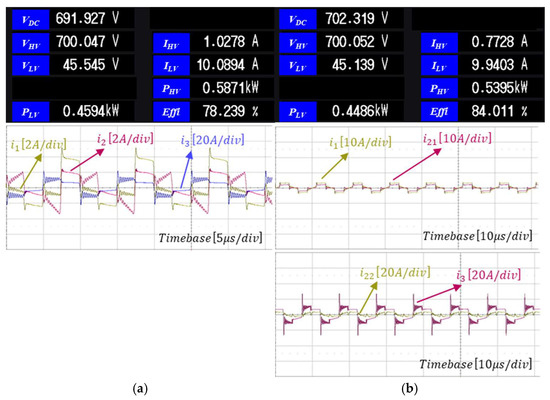
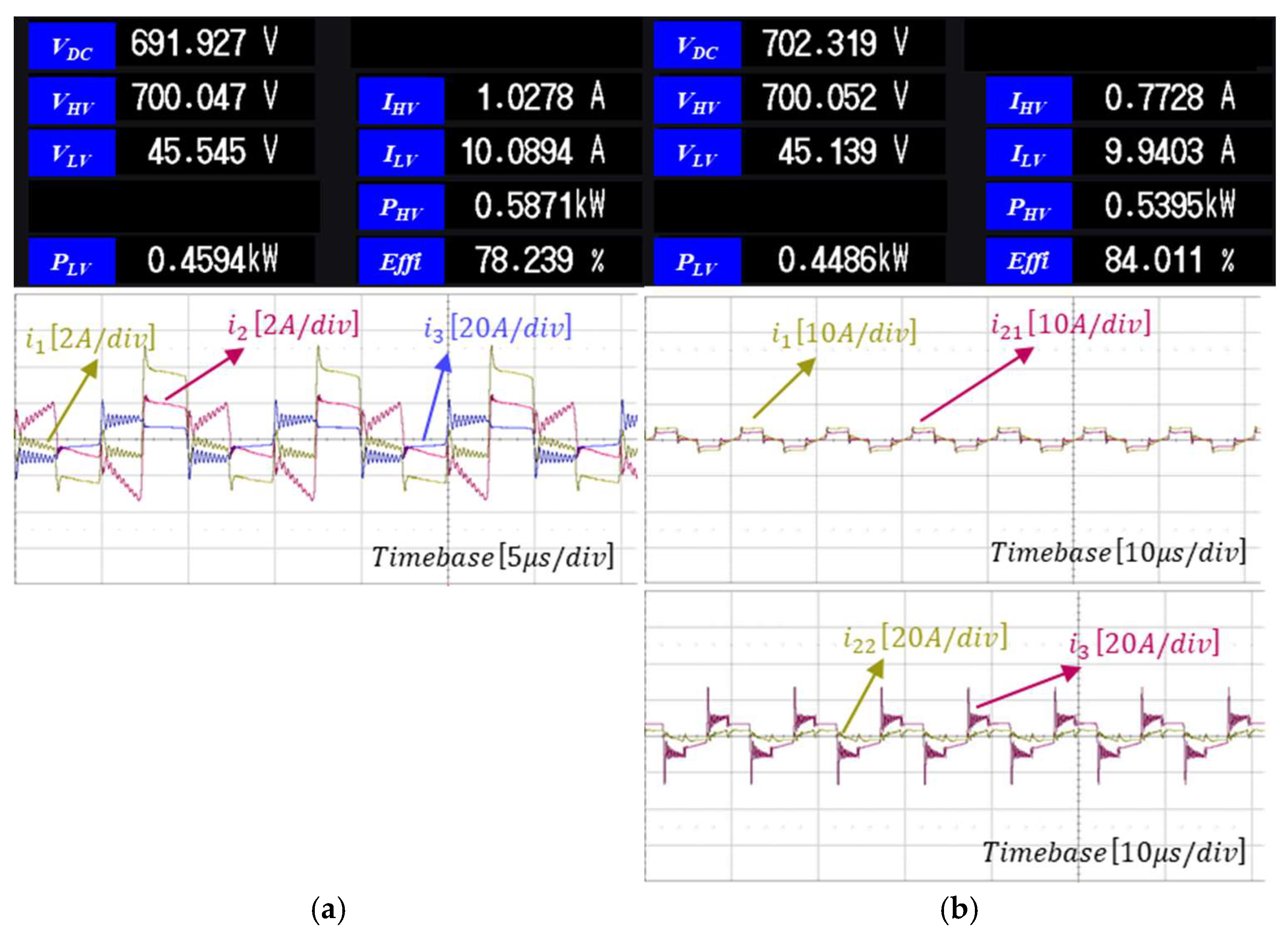
Figure 18 presents the experimental results under the 15% light-load conditions during standalone LDC operation. Under this operating mode, the low load level causes transformer core loss to become the dominant contributor to the overall system losses. In the experimental results of the three-winding transformer-based system shown in Figure 18a, hard-switching operation occurs in the lagging leg of the OBC secondary-side bridge, and the system achieves an efficiency of 78.24%. In contrast, the proposed system achieves ZVS operation for all switches and attains a significantly higher efficiency of 84%.
Figure 18.
LDC standalone operation light-load (450 W) experimental results: (a) 3-winding trans system; (b) proposed system.
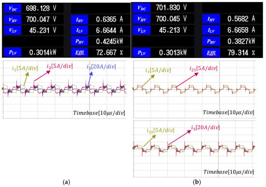
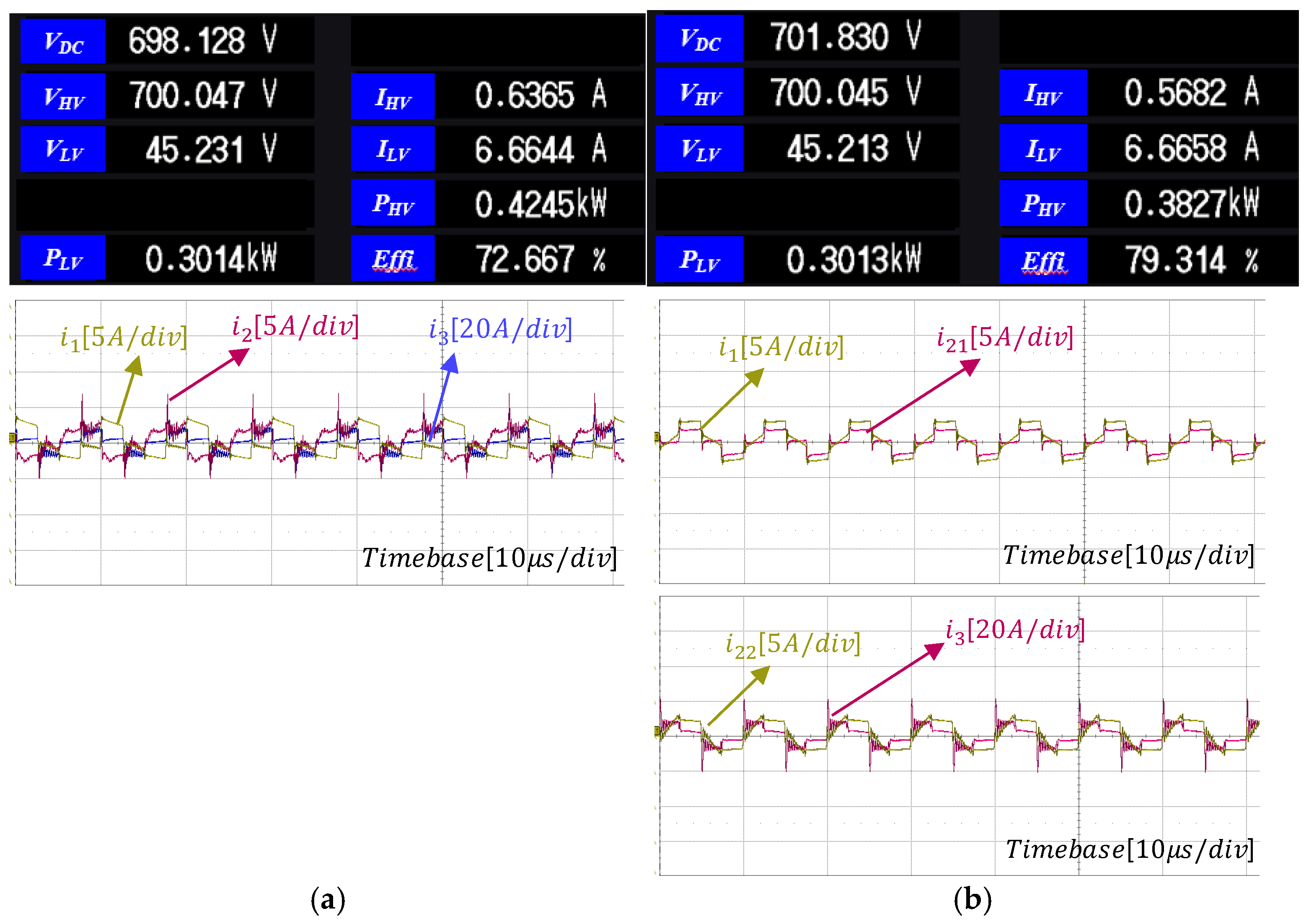
Figure 19 presents the experimental results under the 10% light-load condition during standalone LDC operation. Similarly to the previous experimental results, the proposed system achieves an efficiency improvement of approximately 6.7%. In addition to achieving ZVS operation for all switches, the proposed system effectively reduces transformer core loss.
Figure 19.
LDC standalone operation light-load (300 W) experimental results: (a) 3-winding trans system; (b) proposed system.
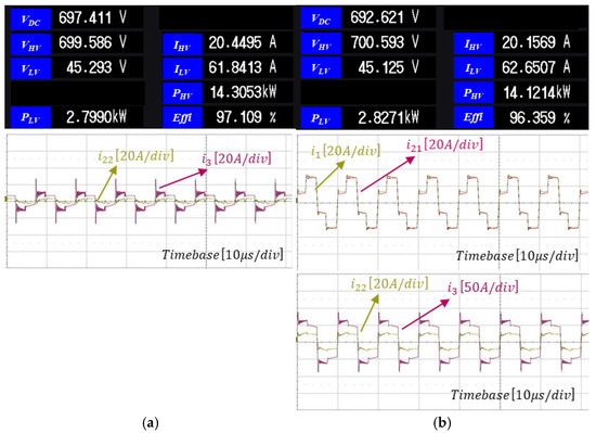
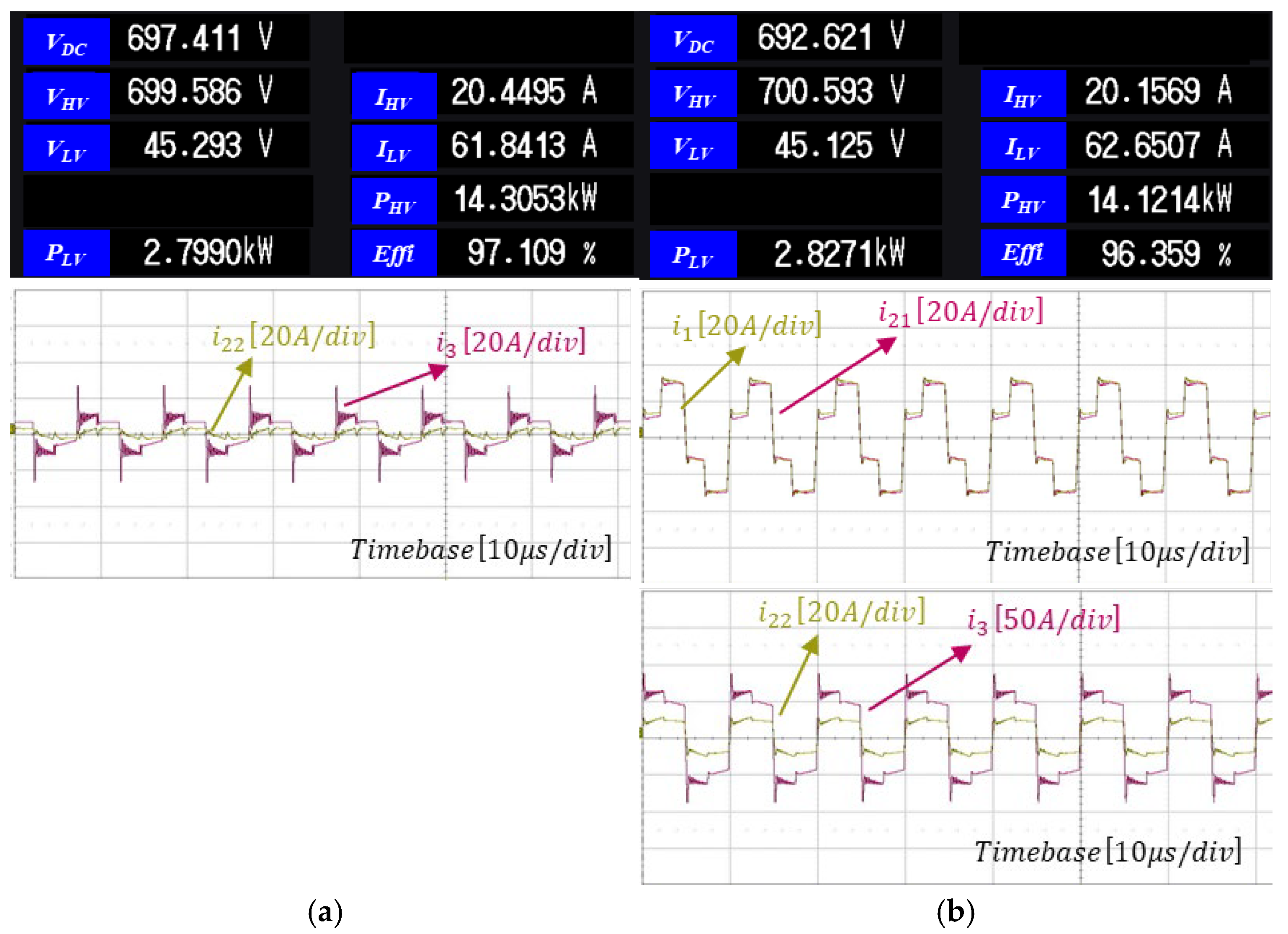
Figure 20 presents the experimental results under simultaneous OBC–LDC operation. In this operating mode, the combined loss characteristics of the transformers and power semiconductor devices directly influence the overall system efficiency. In the experimental results of the three-winding transformer-based system shown in Figure 19a, the system achieves an efficiency of 97.11%, whereas the proposed system shown in Figure 19b achieves an efficiency of 96.36%. This difference arises from higher core loss in the OBC transformer of the proposed system compared to the three-winding transformer, as well as increased diode loss on the LDC side. However, the proposed system focuses primarily on improving light-load loss performance during standalone LDC operation. Owing to the enhanced transformer design flexibility provided by the 2-Trans architecture, the observed efficiency reduction under simultaneous operation can be sufficiently mitigated through further optimization. Table 8 summarizes the overall experimental results and presents a comparison of power density. The proposed system and the conventional three-winding transformer-based system exhibit nearly identical power density, while the 2-Trans structure enables flexible design trade-offs between power density and efficiency depending on specific design objectives.
Figure 20.
OBC–LDC simultaneous operation (14 kW) experimental results: (a) 3-winding trans system; (b) proposed system.
Table 8.
Summary of experimental results.
5. Conclusions
This paper proposes a novel integrated OBC–LDC charging system based on a 2-Trans architecture, in which independent transformers are applied to the OBC and LDC to address the light-load loss issue in the LDC standalone operating mode and the limited transformer design flexibility of conventional three-winding transformer-based systems for electric vehicles. The operating principle of the proposed system is analyzed, and an equivalent circuit model is developed. Based on this model, the power transfer characteristics under different operating modes are derived using a DPS control scheme. In addition, a transformer design methodology is presented and evaluated through FEM simulations. To verify the feasibility of the proposed system, a 100 kHz prototype is implemented, and experimental results demonstrate that the system can simultaneously deliver 11 kW and 3 kW to the high-voltage and low-voltage batteries, respectively. A quantitative performance comparison with a conventional three-winding transformer-based integrated system confirms that the proposed structure improves efficiency by approximately 0.2% under rated load conditions and by about 6% under light-load conditions during standalone LDC operation. These results clearly demonstrate the effectiveness of the proposed architecture in reducing light-load losses, which have a significant impact on overall energy consumption in electric vehicle applications. Integrated charging systems for electric vehicles require both high power density and high efficiency, and improving the efficiency of the LDC standalone operating mode is particularly critical due to its dominant contribution to cumulative energy losses. Although the proposed system exhibits slightly lower efficiency under simultaneous OBC–LDC operation, the enhanced transformer design flexibility enabled by the 2-Trans structure allows further optimization to mitigate this limitation. Therefore, the proposed integrated charging system represents an effective alternative that overcomes the limitations of conventional integrated structures while achieving high efficiency and improved design flexibility. Future work will focus on further enhancing the efficiency of the simultaneous OBC–LDC operating mode through optimized transformer.
Author Contributions
Conceptualization, Y.L., S.K. and D.-H.K.; methodology, Y.L. and S.K.; validation, Y.L., S.K., M.-J.K. and H.-K.S.; formal analysis, Y.L., S.K., M.-J.K. and H.-K.S.; investigation, Y.L. and S.K.; writing—original draft preparation, Y.L. and S.K.; writing—review and editing, Y.L., S.K. and D.-H.K. All authors have read and agreed to the published version of the manuscript.
Funding
This work was supported by the National Research Foundation of Korea (NRF) grant funded by the Korea government (MSIT) (RS-2025-00518217) and by the Korea Institute of Energy Technology Evaluation and Planning(KETEP) and the Ministry of Trade, Industry & Energy(MOTIE) of the Republic of Korea. (No. RS-2025-07852969).
Institutional Review Board Statement
Not applicable.
Informed Consent Statement
Not applicable.
Data Availability Statement
The data presented in this study are available on request from the corresponding author. The data are not publicly available due to privacy.
Conflicts of Interest
Authors Min-Jung Kim and Hee-Keun Shin were employed by Hyundai KEPICO. The remaining authors declare that the research was conducted in the absence of any commercial or financial relationships that could be construed as a potential conflict of interest.
References
- Fesli, U.; Ozdemir, M.B. Electric Vehicles: A Comprehensive Review of Technologies, Integration, Adoption, and Optimization. IEEE Access 2024, 12, 140908–140931. [Google Scholar] [CrossRef] [Scilit]
- Habib, S.; Khan, M.M.; Abbas, F.; Ali, A.; Faiz, M.T.; Ehsan, F.; Tang, H. Contemporary trends in power electronics converters for charging solutions of electric vehicles. CSEE J. Power Energy Syst. 2020, 6, 911–929. [Google Scholar] [CrossRef] [Scilit]
- Mo, T.; Li, Y.; Lau, K.-T.; Poon, C.K.; Wu, Y.; Luo, Y. Trends and Emerging Technologies for the Development of Electric Vehicles. Energies 2022, 15, 6271. [Google Scholar] [CrossRef] [Scilit]
- Rana, M.M.; Alam, S.M.M.; Rafi, F.A.; Deb, S.B.; Agili, B.; He, M.; Ali, M.H. Comprehensive Review on the Charging Technologies of Electric Vehicles (EV) and Their Impact on Power Grid. IEEE Access 2025, 13, 35124–35156. [Google Scholar] [CrossRef] [Scilit]
- Yilmaz, M.; Krein, P.T. Review of Battery Charger Topologies, Charging Power Levels, and Infrastructure for Plug-In Electric and Hybrid Vehicles. IEEE Trans. Power Electron. 2013, 28, 2151–2169. [Google Scholar] [CrossRef] [Scilit]
- Su, W.; Eichi, H.; Zeng, W.; Chow, M.Y. A survey on the electrification of transportation in a smart grid environment. IEEE Trans. Ind. Inf. 2012, 8, 1–10. [Google Scholar]
- Islam, R.; Rafin, S.M.S.H.; Mohammed, O.A. Comprehensive Review of Power Electronic Converters in Electric Vehicle Applications. Forecasting 2023, 5, 22–80. [Google Scholar] [CrossRef] [Scilit]
- Baharom, R.; Hayroman, M.H. A Comprehensive Review on Advancements in Battery Charger Technologies for Electric Vehicles. In Proceedings of the 2024 IEEE Industrial Electronics and Applications Conference (IEACon), Kuala Lumpur, Malaysia, 4–5 November 2024; pp. 190–195. [Google Scholar] [CrossRef] [Scilit]
- Hong, S.; Zeng, Y. A health assessment framework of lithium-ion batteries for cyber defense. Appl. Soft Comput. 2021, 101, 107067. [Google Scholar] [CrossRef] [Scilit]
- Wang, P.; Wu, X.; He, X. Vibration-Theoretic Approach to Vulnerability Analysis of Nonlinear Vehicle Platoons. IEEE Trans. Intell. Transp. Syst. 2023, 24, 11334–11344. [Google Scholar] [CrossRef] [Scilit]
- Kim, Y.-S.; Oh, C.-Y.; Sung, W.-Y.; Lee, B.K. Topology and Control Scheme of OBC–LDC Integrated Power Unit for Electric Vehicles. IEEE Trans. Power Electron. 2017, 32, 1731–1743. [Google Scholar] [CrossRef] [Scilit]
- Kim, S.; Kang, F.-S. Multi-functional On-board Battery Charger for Plug-in Electric Vehicles. IEEE Trans. Ind. Electron. 2015, 62, 3460–3472. [Google Scholar] [CrossRef] [Scilit]
- Wang, H.; Shang, M.; Khaligh, A. A PSFB-Based Integrated PEV Onboard Charger With Extended ZVS Range and Zero Duty Cycle Loss. IEEE Trans. Ind. Appl. 2017, 53, 585–595. [Google Scholar] [CrossRef] [Scilit]
- Singh, D.C.D.R.; R, N.; Aldahmashi, J.; Yousef, A. Integrated On-Board Charger, Wireless Charging and Auxiliary Power Topologies for EVs: A Survey. Energies 2026, 19, 689. [Google Scholar] [CrossRef] [Scilit]
- Kougioulis, I.; Pal, A.; Wheeler, P.; Ahmed, R. An Isolated Multiport DC–DC Converter for Integrated Electric Vehicle On-Board Charger. IEEE J. Emerg. Sel. Top. Power Electron. 2023, 11, 4178–4198. [Google Scholar] [CrossRef] [Scilit]
- Tang, Y.; Lu, J.; Wu, B.; Zou, S.; Ding, W.; Khaligh, A. An Integrated Dual-Output Isolated Converter for Plug-in Electric Vehicles. IEEE Trans. Veh. Technol. 2018, 67, 966–976. [Google Scholar] [CrossRef] [Scilit]
- Chakraborty, S.S.; Dey, S.; Hatua, K. Design of a Three-Winding Transformer for Power Decoupling of a Three-Port Series Resonant Converter for an Integrated On-Board EV Charger. IEEE Trans. Power Electron. 2023, 38, 14262–14273. [Google Scholar] [CrossRef] [Scilit]
- Kougioulis, I.; Vannini, A.; Pal, A.; Wheeler, P.; Ahmed, M.R. Estimation of Leakage Inductance in High-frequency Three-Winding Transformers for Electric Vehicle On-board Chargers. In Proceedings of the 25th European Conference on Power Electronics and Applications (EPE’23 ECCE Europe), Aalborg, Denmark, 4–8 September 2023; pp. 1–11. [Google Scholar] [CrossRef] [Scilit]
- Zhao, B.; Song, Q.; Liu, W. Efficiency Characterization and Optimization of Isolated Bidirectional DC–DC Converter Based on Dual-Phase-Shift Control for DC Distribution Application. IEEE Trans. Power Electron. 2013, 28, 1711–1727. [Google Scholar] [CrossRef] [Scilit]
- Nguyen, H.V.; Lee, D. An improved low-voltage charging circuit for single-phase onboard battery chargers. In Proceedings of the 2019 IEEE Applied Power Electronics Conference and Exposition (APEC), Anaheim, CA, USA, 17–21 March 2019; pp. 3325–3331. [Google Scholar]
- Chakkalakkal, S.; Kozielski, K.; Taha, W.; Wang, Y.; Anand, A.; Emadi, A. Loss-Optimized Design of a Triple Active Bridge DC-DC Converter for an Electric Vehicle Application. In Proceedings of the 2025 IEEE Applied Power Electronics Conference and Exposition (APEC), Atlanta, GA, USA, 16–20 March 2025; pp. 3147–3154. [Google Scholar] [CrossRef] [Scilit]



Disclaimer/Publisher’s Note: The statements, opinions and data contained in all publications are solely those of the individual author(s) and contributor(s) and not of MDPI and/or the editor(s). MDPI and/or the editor(s) disclaim responsibility for any injury to people or property resulting from any ideas, methods, instructions or products referred to in the content. |
© 2026 by the authors. Licensee MDPI, Basel, Switzerland. This article is an open access article distributed under the terms and conditions of the Creative Commons Attribution (CC BY) license.