


Abstract
ZnS is one of the most promising wide-bandgap semiconductors for optoelectronic and sensing applications owing to its efficient ultraviolet–blue emission, high exciton binding energy, and chemical stability. However, the synthesis of ZnS nanocrystals in silicon-compatible porous matrices remains largely unexplored. In this work, ordered arrays of ZnS nanocrystals were synthesized for the first time in SiO2/Si track templates fabricated by swift heavy ion irradiation followed by selective chemical etching. ZnS nanocrystals were deposited by electrochemical deposition from aqueous solutions containing ZnCl2 and thiourea precursors. The structural, optical, and electrical properties of the resulting ZnS/SiO2/Si nanocomposites were investigated using scanning electron microscopy, X-ray diffraction, Raman spectroscopy, photoluminescence spectroscopy, and electrical measurements. The fabricated templates contained vertically aligned pores with a density of approximately 108 cm−2 and an average diameter of about 500 nm. Electrochemical deposition resulted in a pore filling efficiency of approximately 88%. X-ray diffraction analysis confirmed the formation of crystalline ZnS with a cubic zinc blende structure. The nanocomposites exhibit intense ultraviolet–blue photoluminescence in the 335–477 nm range, with pronounced emission peaks at 372 and 400 nm characteristic of ZnS nanocrystals. Current–voltage measurements indicate predominantly electronic conductivity, with a conductivity of 1.54 × 10⁻⁶ Ohm−1·cm−1, comparable to values reported for polycrystalline ZnS films. To support the experimental observations, the electronic structure of ZnS was analyzed using density functional theory within the LCAO framework. The calculated bandgap of 3.4 eV is consistent with previously reported theoretical and experimental data. The obtained results demonstrate that SiO2/Si track templates provide a promising platform for the fabrication of ordered ZnS nanoarrays with potential applications in silicon-compatible optoelectronic and sensing devices.
1. Introduction
Binary II–VI semiconductor nanomaterials have attracted considerable attention because of their versatile optical, electronic, and chemical properties. Among them, zinc chalcogenides occupy a special position due to their relatively low toxicity, high photoluminescence efficiency, good chemical stability, and broad applicability in optoelectronics, sensing, photocatalysis, and energy-related technologies [1,2,3,4,5,6,7,8,9,10,11,12]. Continuous progress in these fields has stimulated the development of synthesis approaches capable of controlling crystal structure, morphology, dimensionality, and surface properties of zinc chalcogenide nanostructures [13,14,15,16,17].
ZnS is one of the most widely studied members of the zinc chalcogenide family owing to its wide direct bandgap (3.5–3.8 eV), large exciton binding energy, and efficient emission in the ultraviolet and blue spectral regions [12,13,14]. These characteristics make ZnS a promising material for photodetectors, light-emitting devices, sensors, photocatalysts, and other optoelectronic applications. Numerous fabrication methods have been developed for ZnS nanostructures, including chemical, physical, and electrochemical approaches [13,14,15,16,17]. Among them, electrochemical deposition (ECD) is particularly attractive because of its simplicity, low cost, scalability, environmental compatibility, and ability to produce nanostructures directly on technologically relevant substrates [17,18,19,20,21,22,23,24,25,26,27].
Template-assisted electrochemical deposition is an efficient strategy for fabricating ordered arrays of semiconductor nanostructures with controlled dimensions and spatial organization. Various porous templates, including anodic aluminum oxide (AAO), porous silicon, and polymer track membranes, have been successfully employed for this purpose [28]. It is worth mentioning the synthesis of ZnS nanocrystals in AAO template by the electrochemical deposition method [29], as well as the polymer-templated synthesis of ZnS nanocrystals by chemical deposition [30]. Despite their widespread use, these template systems suffer from several limitations, including mechanical fragility, limited thermal stability, oxidation issues, or difficulties associated with integration into standard silicon-based technologies. Therefore, the development of silicon-compatible template platforms for ZnS growth remains an important challenge.
An attractive alternative is provided by SiO2/Si track templates fabricated using swift heavy ion irradiation followed by selective chemical etching [31]. Such templates combine the advantages of track-etched porous systems with the technological compatibility of the Si/SiO2 platform. In addition to their chemical and thermal stability, SiO2/Si templates offer the possibility of forming ordered semiconductor nanoarrays directly on silicon substrates and creating nanoscale semiconductor–semiconductor or metal–semiconductor junctions relevant for future electronic and photonic devices [31,32,33,34,35,36].
The potential of SiO2/Si track templates has already been demonstrated for the fabrication of various metallic and semiconductor nanostructures. Ordered arrays of Ni, Co, Ag, Cu, and Au nanostructures have been successfully synthesized in these matrices [32,33,34,35,36]. More recently, semiconductor oxides and chalcogenides, including ZnO, SnO2, Ga2O3, ZnSe, ZnSeO3, CdTe, CdO, PbTe, and CdS, have been fabricated using chemical and electrochemical deposition approaches [37,38,39,40,41,42,43,44]. These studies have confirmed that the SiO2/Si platform is suitable for producing functional nanocomposites with promising optical and electrical properties.
However, despite the technological importance of ZnS and the successful synthesis of several related semiconductor compounds in SiO2/Si templates, the fabrication of ZnS nanocrystals within this platform has not yet been reported. Consequently, the influence of geometrical confinement in SiO2 nanochannels on the structural, optical, and electrical properties of ZnS nanocrystals remains largely unexplored. Addressing this gap is important both for understanding the growth mechanisms of confined ZnS nanostructures and for evaluating their potential in silicon-compatible optoelectronic and sensing applications.
In the present work, we report the first synthesis of ordered ZnS nanocrystal arrays in SiO2/Si track templates by electrochemical deposition. The structural, optical, and electrical properties of the resulting ZnS/SiO2/Si nanocomposites are systematically investigated. In addition, density functional theory calculations are employed to provide insight into the electronic structure of ZnS nanocrystals and to support the interpretation of the experimental results.
2. Materials and Methods
A silicon dioxide (SiO2) layer with a thickness of approximately 700 nm was thermally grown on an n-type Si (100) substrate in a wet oxygen atmosphere at 900 °C. Subsequently, square samples measuring 1 × 1 cm2 were prepared from the oxidized wafers and irradiated with 177 MeV Xe ions at the DC-60 heavy ion accelerator (Astana, Kazakhstan) to a fluence of 1 × 10⁸ ions/cm2. In recent years, this facility has demonstrated high efficiency for investigating radiation-induced defects and ion-track formation processes in various materials [45,46,47,48,49,50,51,52]. At the selected fluence, ion-track overlap is negligible, while the concentration of irradiation-induced background defects remains insignificant [53,54,55]. Prior to the track-etching procedure, the sample surfaces were ultrasonically cleaned in isopropanol for 10 min to remove contaminants. Nanoporous templates were subsequently fabricated by selectively etching the latent ion tracks in the SiO2 layer using a 4 wt.% aqueous hydrofluoric acid (HF) solution containing palladium chloride (PdCl2) at room temperature. Following the etching process, the templates were thoroughly rinsed with deionized water (18.2 MΩ·cm) and dried under ambient conditions. It should be noted that, during treatment in an etching solution, not only does the accelerated etching of the latent track areas occur, but also the dissolution of the intact SiO2 layer. To evaluate the decrease in the template thickness during etching, the original SiO2 (700 nm)/Si sample with the surface half-covered with wax was treated in the same HF solution for 10 min. The step height between the protected and unprotected surfaces of the original sample after etching for 10 min was ~180 nm. Hence, the resulting thickness of SiO2 after etching was ~520 nm.
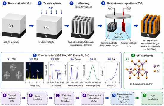
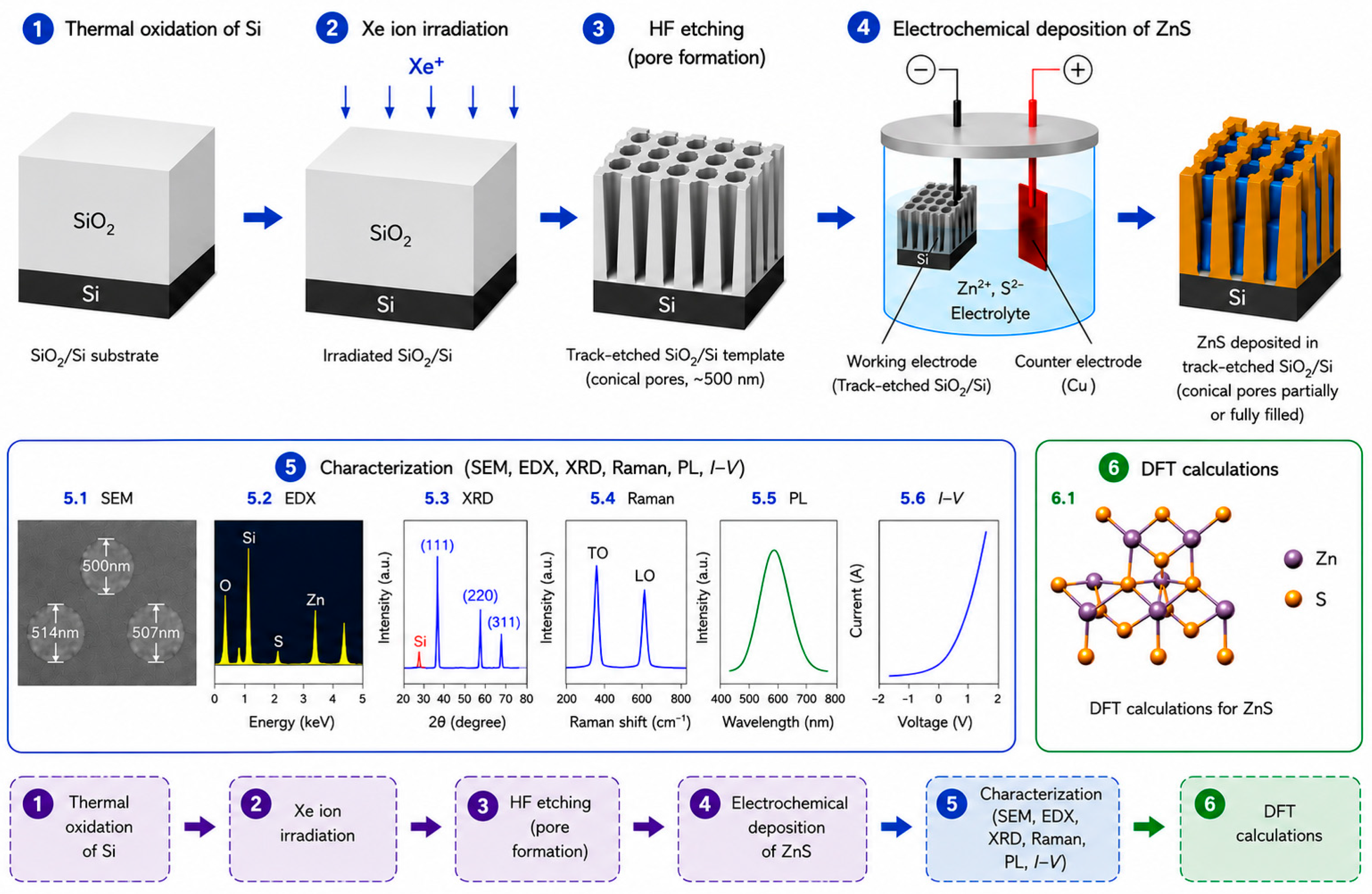
A schematic representation of the fabrication route of the ZnS/SiO2/Si nanocomposites and the subsequent characterization procedures is shown in Figure 1. The workflow includes template preparation by ion-track technology, electrochemical deposition of ZnS, structural and optical characterization, and theoretical calculations.
Figure 1.
Schematic illustration of the fabrication process of ZnS/SiO2/Si nanocomposites, including thermal oxidation of silicon, Xe ion irradiation, HF etching, electrochemical deposition of ZnS, characterization, and DFT calculations. The different colors of the arrows, boxes, and frames are used for visual clarity only and do not indicate any additional physical meaning.
As shown in Figure 1, the fabrication procedure consists of several consecutive stages, including thermal oxidation of silicon, Xe-ion irradiation, formation of track-etched SiO2/Si templates by HF etching, electrochemical deposition of ZnS, and subsequent structural, optical, and electrical characterization. In addition, density functional theory (DFT) calculations were performed to support the interpretation of the experimental results.
Zinc chloride (ZnCl2, Sigma-Aldrich, St. Louis, MO, USA), thiourea (SC(NH2)2, Sigma-Aldrich, St. Louis, MO, USA), ammonia solution (NH4OH, Sigma-Aldrich, St. Louis, MO, USA), hydrofluoric acid (HF, Sigma-Aldrich, St. Louis, MO, USA), and palladium chloride (PdCl2, Sigma-Aldrich, St. Louis, MO, USA) were used as received without further purification. A solution for the electrochemical deposition of ZnS into the a-SiO2 pores/Si-n track template was prepared as follows. Fifty milliliters of an aqueous zinc chloride solution (ZnCl2, 1.72 g/L) was mixed with 50 mL of an aqueous thiourea solution (SC(NH2)2, 1.53 g/L) and stirred for 10 min. Subsequently, ammonia solution was added dropwise until the solution turned white. Thereafter, ZnS was electrodeposited at pH = 12 in an electrochemical cell using copper electrodes as the working and counter electrodes for 10 min under potentiostatic conditions at an applied voltage of 1.75 V.
The formation of ZnS during electrochemical deposition is governed by a sequence of complexation and precipitation reactions. Ammonia acts as a complexing agent and forms zinc–ammonia complexes according to the following:
This process reduces the concentration of free Zn2+ ions in the electrolyte and prevents their rapid precipitation in the bulk solution. Under alkaline conditions (pH = 12), thiourea gradually decomposes, releasing sulfur-containing species, which subsequently react with zinc ions to form ZnS:
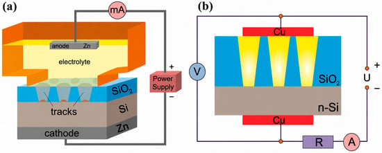
Therefore, ammonia stabilizes the electrolyte composition and promotes controlled nucleation and uniform growth of ZnS nanocrystals inside the confined SiO2 nanochannels. The deposition process was carried out at room temperature without stirring. Figure 2a depicts the schematic image of a cell. After ECD, the samples were washed in deionized water and dried in air.
Figure 2.
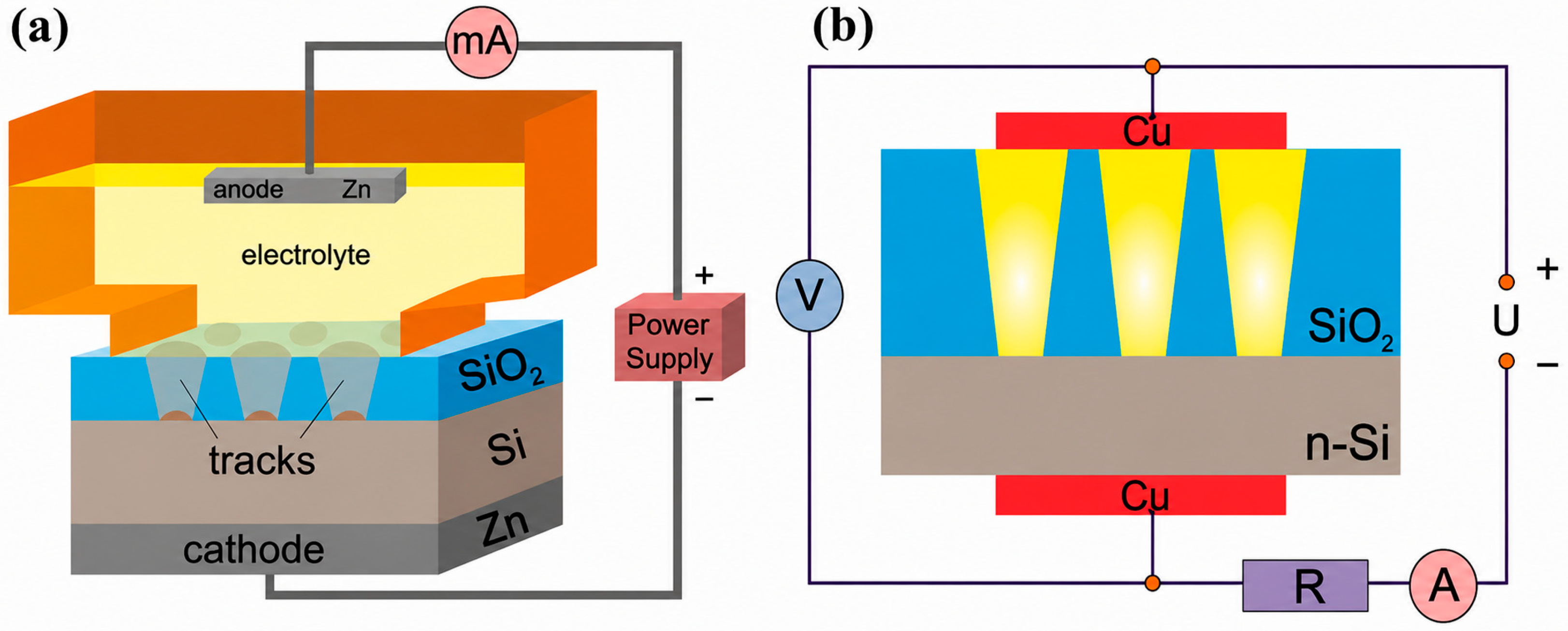
The scheme of the electrochemical cell for ZnS deposition (a) and the scheme of the setup for current–voltage characteristics’ measurements (b).
To study the electrophysical properties, the current–voltage characteristics (CVC) of the samples with deposited precipitates were measured. To enable electrical measurements, copper contacts with an area of 0.3 cm2 were deposited by thermal evaporation onto the surface containing the pore-filled layer. An identical electrode was subsequently fabricated on the opposite side of the sample, resulting in a symmetric contact configuration. Then the electrodes were connected to an HP 66312A current source in series with an Agilent 34401A multimeter (Agilent Technologies, Inc., Santa Clara, CA, USA). The measurement scheme is shown in Figure 2b.
The surface microstructure of the samples was studied using a JEOL JSM-7500F scanning electron microscope (JEOL Ltd., Tokyo, Japan). Elemental analysis was performed using an energy-dispersive microanalyzer combined with a Hitachi TM3030 microscope (Hitachi High-Tech Corporation, Tokyo, Japan). A Rigaku Miniflex 600 X-ray diffractometer (Rigaku Corporation, Tokyo, Japan) with a copper anode was used to study the crystal structure of the deposited precipitates. Registration of the X-ray spectra was carried out in the angular range 2θ from 20 to 60° with a step of 0.01° using the Bruker AXSDIFFRAC.EVAv.4.2 software (Bruker AXS GmbH, Karlsruhe, Germany), and phase identification was carried out according to the international ICDD PDF-2 database.
Raman measurements were carried out using an NTegra Spectra system (NT-MDT Spectrum Instruments, Moscow, Russia) equipped with a 473 nm blue excitation laser. Spectral acquisition was performed with an 1800 lines/mm diffraction grating, providing a resolution of approximately 1 cm−1. The laser was focused on the sample into a spot with a diameter of 2 μm; the signal accumulation time was 100–200 s. The baseline correction and intensity normalization of Raman spectra were performed in order to eliminate background noise and ensure correct comparison of peak intensities. The PL spectra were recorded at room temperature (300 K) in the range from 300 to 800 nm using a CM 2203 spectrofluorimeter (Solar, Minsk, Belarus) with excitation by Xe-lamp radiation with a wavelength of 240 nm. In all cases, the emission of the initial SiO2 porous/Si template was subtracted from the PL spectrum of the template with deposited precipitates.
Finally, large-scale ab initio calculations were performed using a linear combination of atomic orbitals method within density functional theory (LCAO-DFT) approach [56,57], as implemented in the CRYSTAL computer code [58]. The pure DFT Perdew–Burke–Ernzerhof functional (PBE) [59] and hybrid B3LYP functionals were chosen, allowing us to perform accurate calculations of the band structure. The all-electron basis sets with BSSE-correction scheme for Zn and S atoms were taken from the CRYSTAL database [60]. The force gradients with respect to atomic coordinates and lattice parameters were evaluated analytically. Convergence in the geometry optimization process was tested using the root-mean-square (rms) and the absolute value of the largest component of both the gradients and nuclear displacements. For all atoms, the thresholds for the maximum and the rms forces were set to 0.000450 and 0.000300 au, while those for the maximum and the rms atomic displacements were chosen to be 0.001800 and 0.001200 au, respectively. The equilibrium structure was determined using a quasi-Newton algorithm with a Broyden–Fletcher–Goldfarb–Shanno Hessian updating scheme [58]. Convergence in the geometry optimization process was tested on the root-mean-square (RMS) and the absolute value of the largest component of both gradients and nuclear displacements. For a self-consistent field (SCF) procedure, the cut-off limits in the evaluation of Coulomb and exchange series have been chosen to be 10−7, 10−7, 10−7, 10−7 and 10−14 a.u. for calculations of the Coulomb overlap, Coulomb penetration, exchange overlap, first exchange pseudo-overlap and second exchange pseudo-overlap integrals, respectively. Total energy difference between two SCF steps (10−7 au) also has a high tolerance of accuracy. The effective charges on atoms were estimated using the Mulliken population analysis [61]. The integration over the Brillouin zone in the reciprocal space was conducted within an 8 × 8 Pack–Monkhorst grid [62].
3. Results
3.1. Morphology and Structure
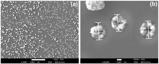
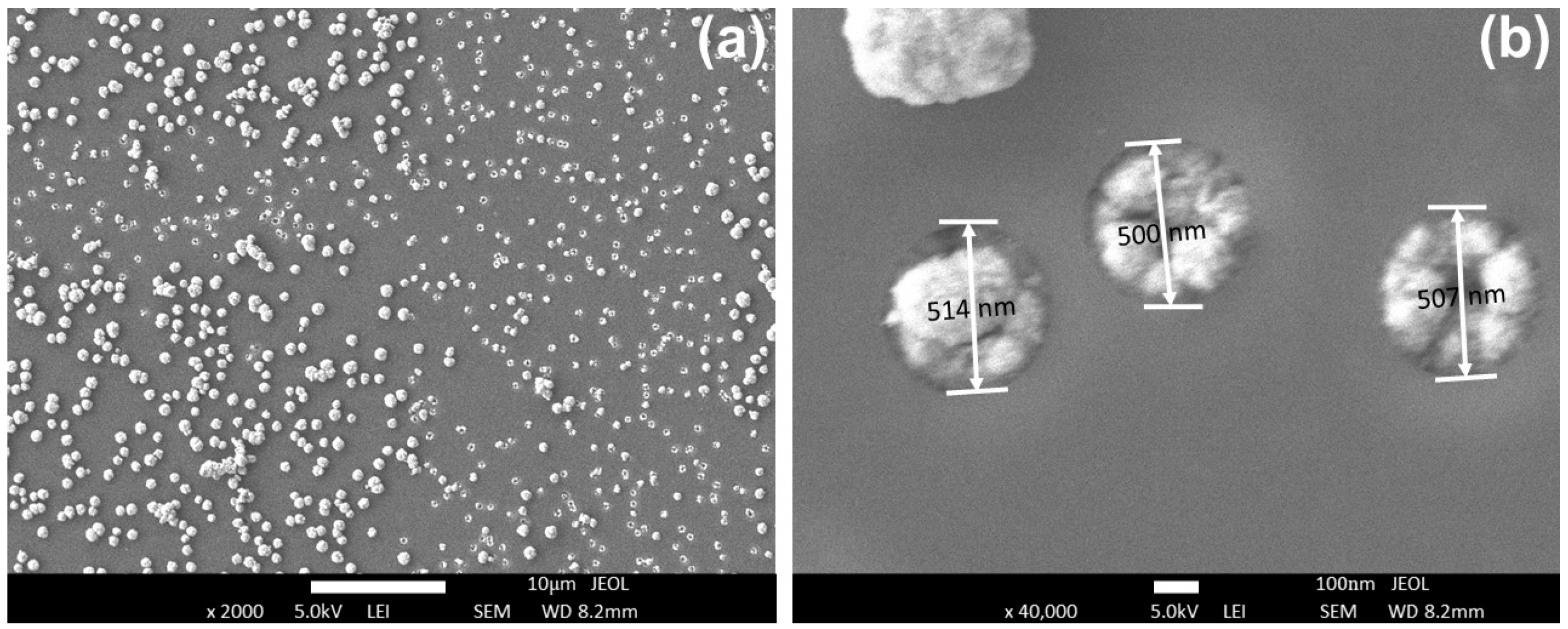
Figure 2 shows SEM images of the template surface at different scales after ECD for 10 min. Analysis of SEM images showed that the degree of filling of pores after ECD for 10 min is ~88%. The pore filling degree was estimated as the ratio of the volume occupied by the deposited material inside the pores to the total pore volume, according to In this approach, partially filled pores contribute proportionally to the calculated filling degree, whereas surface outgrowths are not treated as an independent contribution since they originate from material deposited within the pores.
Figure 3b shows pores with a diameter of ~500 nm exhibiting a high degree of filling with deposited material. However, since SEM provides information primarily about the surface morphology, the complete filling of the pores throughout the template thickness cannot be directly confirmed. It can be seen that the deposited material has a dense granular structure, often with deepening in the centers of filled pores. The semispherical “caps” with larger diameter on the surface of SiO2 are also observed (Figure 3a), which is associated with the protrusion of the deposited material onto the sample’s surface from the filled pores. The presence of surface protrusions and partially filled pores in the SiO2 matrix can lead to nonuniform electrical and emission characteristics of the resulting nanocomposites. Therefore, additional optimization of the deposition conditions may be necessary to improve material growth inside the templates and to ensure more complete pore filling.
Figure 3.
SEM images of template surface with filled pores (a) and individual filled pores (b).
Although the surface SEM images demonstrate a high pore filling efficiency (~88%) and indicate that many pores are completely filled with ZnS precipitates, cross-sectional SEM or TEM investigations would provide more direct information about the morphology and spatial distribution of ZnS nanocrystals throughout the template thickness. Such studies are beyond the scope of the present work and will be the subject of future investigations.
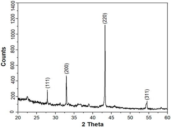
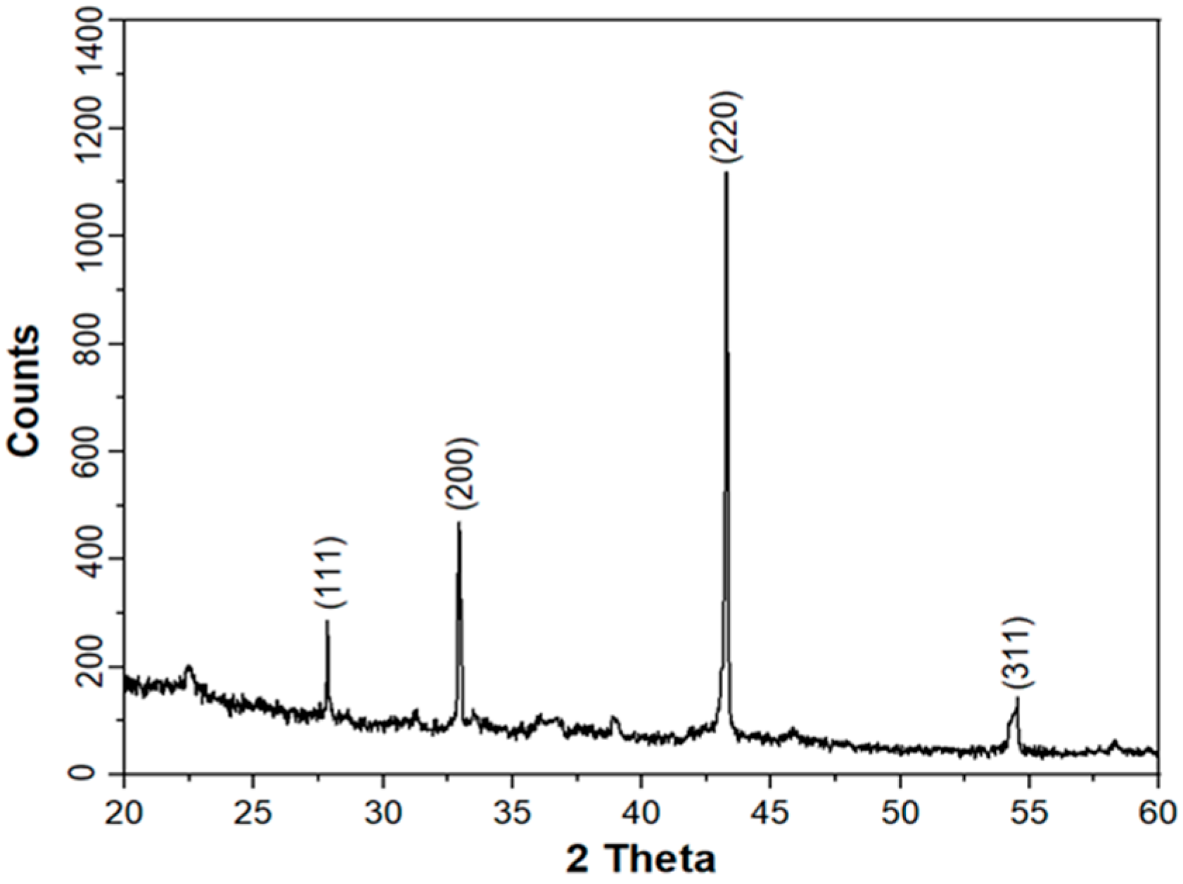
XRD study of the samples with filled templates showed the formation of ZnS nanocrystals with a cubic crystal structure of spatial syngony F-43m (216). Figure 4 shows the X-ray diffraction pattern (XRD) of the deposited precipitates. The crystallographic parameters of the deposited nanocrystals, calculated from XRD data using the international ICDD PDF-2 database for phase identification, are summarized in Table 1.
Figure 4.
The XRD pattern of the precipitates deposited into SiO2/Si template.
Table 1.
The crystallographic parameters of the deposited nanocrystals.
The average lattice parameter calculated from the interplanar distances is 5.62 Å. It is slightly larger than the standard value for bulk ZnS in the zinc blende structure (5.41 Å) [63]. This lattice expansion may be attributed to several factors. One possible contribution is tensile strain induced during growth on the (100)-oriented silicon substrate. However, considering the relatively small lattice mismatch between Si (5.43 Å) and ZnS (5.41 Å) [64], additional contributions from the sulfur-rich composition revealed by EDX analysis, intrinsic point defects, and nanoscale strain effects associated with the nanocrystalline structure should also be considered. These factors may lead to local lattice distortions and contribute to the observed increase in the lattice parameter. It should be noted that the intensity of the (220) reflection exceeds that of the (111) reflection, which deviates from the standard powder diffraction pattern of cubic ZnS where the (111) reflection dominates.
It should be noted that the crystallite size was estimated using the Scherrer equation, which assumes that the diffraction peak broadening originates exclusively from the finite crystallite size. However, the observed peak broadening may also contain a contribution from microstrain associated with lattice distortion and tensile strain induced by the lattice mismatch between ZnS and the Si substrate. Therefore, the calculated crystallite size should be regarded as an approximate estimate of the coherent scattering domain size, and the actual crystallite dimensions may differ from the value obtained using the Scherrer approach.
This suggests the presence of a preferred crystallographic orientation (texture), likely associated with the epitaxial or lattice matching between the ZnS film and the silicon substrate, leading to the preferential alignment of (220) planes parallel to the surface. A similar effect was observed by Valkonen et al. [65] in their study on ZnS films grown on Si (100) using the successive ionic layer adsorption and reaction method, where only a weak (200) reflection was detected. In our case, the use of a Si (100) substrate promoted the growth of ZnS in the (220) orientation. Small trace peaks around 38° are also observed in the XRD pattern, which can be attributed to the (102) plane of the wurtzite phase [66]. This metastable hexagonal phase likely forms during the initial stages of deposition. A small peak also appears at 22° in the spectrum, which is attributed to the SiO2 phase [67].
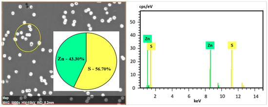
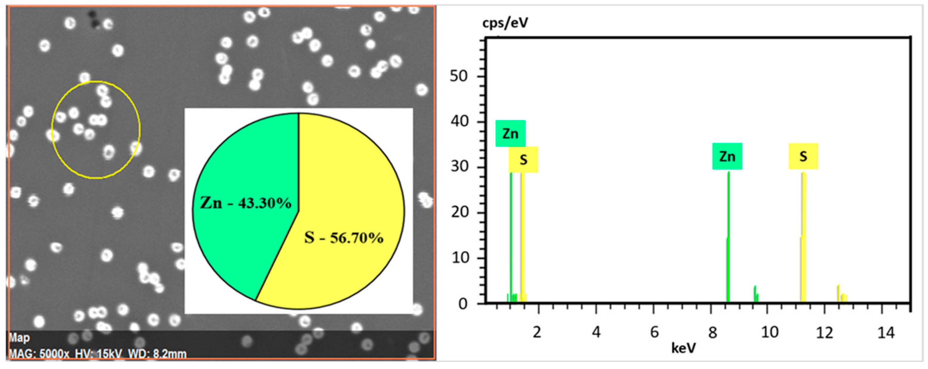
Figure 5 shows the energy-dispersive spectrum of the deposited nanocrystals.
Figure 5.
EDX spectrum of the deposited ZnS precipitates.
As can be seen, the EDX data confirm the results of the XRD study. The spectrum shows peaks only from Zn and S, and the content of Zn and S in the system is 43.3 at.% and 56.7 at.%, respectively, i.e., zinc sulfide is enriched with sulfur compared to stoichiometry. No signal from oxygen (the presence of oxide phases) is observed in the spectrum. The sulfur-rich composition may be related to the excess sulfur species generated during thiourea decomposition under alkaline conditions, leading to the incorporation of sulfur-related defects into the ZnS lattice. Such non-stoichiometry can promote the formation of zinc vacancies (VZn), sulfur antisite defects (SZn), and sulfur interstitials, resulting in local lattice distortions and contributing to the observed lattice expansion. In addition, sulfur-related defects may introduce localized electronic states within the bandgap, thereby affecting the photoluminescence properties of ZnS nanocrystals. The relatively low conductivity of the ZnS nanoarrays may also be influenced by defect-related carrier trapping and scattering processes associated with the sulfur-rich composition.
3.2. Raman Spectroscopy
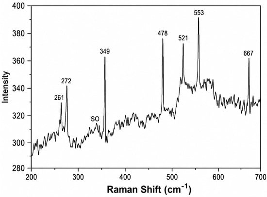
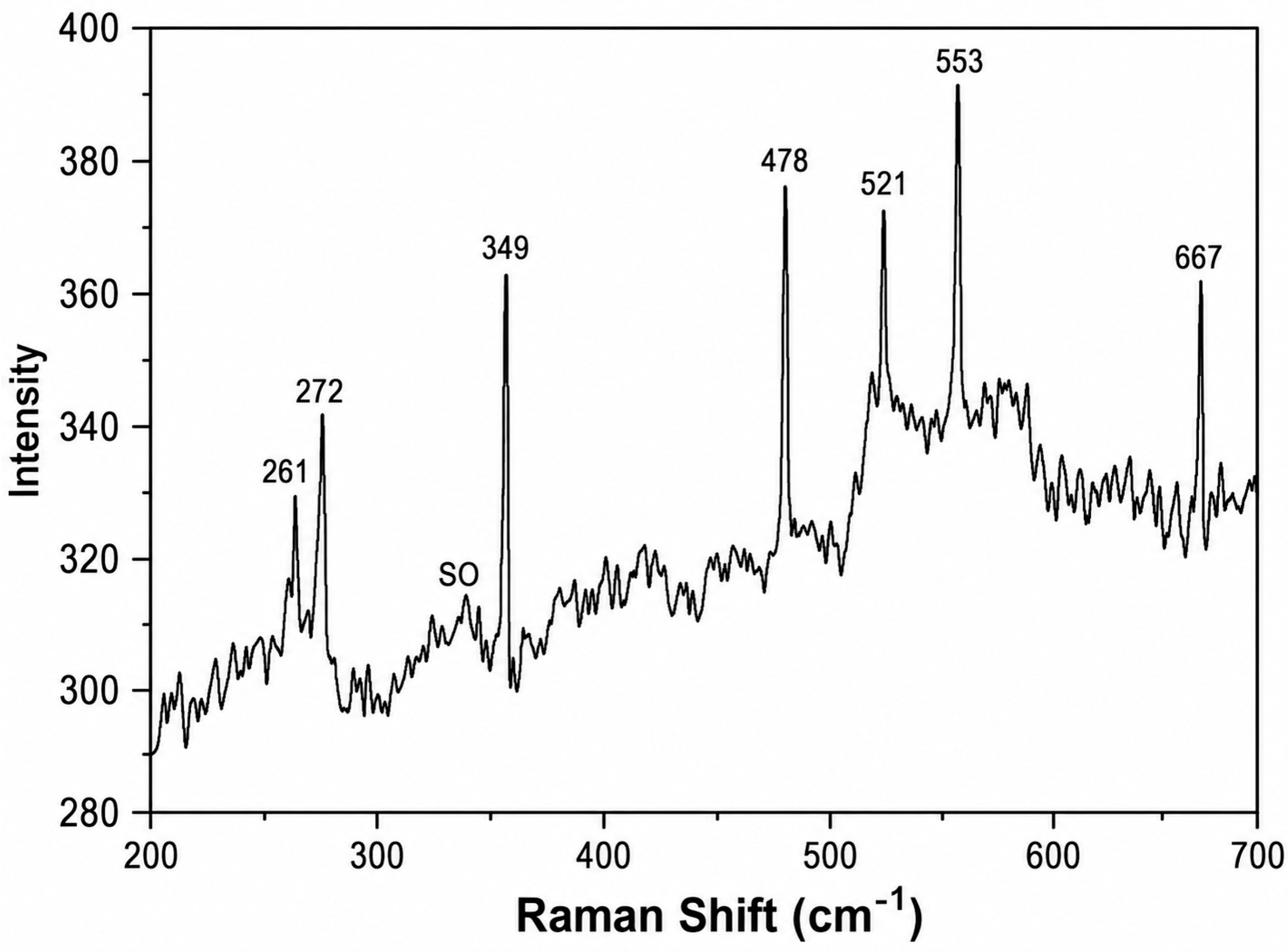
To identify the synthesized precipitates, an additional study was conducted using Raman spectroscopy (RS). Figure 6 depicts the RS spectrum of the SiO2 porous/Si sample with filled pores, and the results of the RS data analysis in comparison with the literature are summarized in Table 2. As can be seen, the Raman spectrum exhibits characteristic peaks at 349 and 272 cm−1, corresponding to scattering on first-order LO and TO phonons in ZnS with a zinc blende structure [68]. The peak at 521 cm−1 is attributed to scattering from the silicon substrate. The remaining peaks can be attributed to combinations of longitudinal and transverse phonons and to second-order phonons characteristic of zinc sulfide. It should be noted that the TO mode is split into two components. This behavior may be associated with crystal lattice distortions induced by strain effects in the ZnS nanocrystals. Such an interpretation is consistent with the XRD results, which indicate lattice expansion relative to bulk ZnS. However, defect-related effects and structural disorder associated with the nanocrystalline nature of the deposited material may also contribute to the observed TO mode splitting. Similar phenomena have been reported in other cubic materials [69,70]. An unusually strong second-order combination Raman scattering observed in our ZnS samples can be attributed to defect- and/or strain-enhanced multiphonon processes [71].
Figure 6.
RS spectrum of the synthesized precipitates.
Table 2.
Features observed in Raman spectra of templates with precipitates and their attribution.
The spectrum also revealed a band at 335 cm−1, which can be assigned to a surface optical (SO) phonon mode [68]. The presence of this mode suggests that surface defects and interfacial interactions with the SiO2/Si matrix play a crucial role in the synthesized nanostructures. Thus, the analysis of the Raman spectra of the samples with deposited precipitates correlates with the X-ray diffraction data and confirms the formation of ZnS nanocrystals with a sphalerite structure by the electrochemical deposition in SiO2 porous/Si templates.
3.3. Photoluminescence
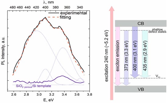
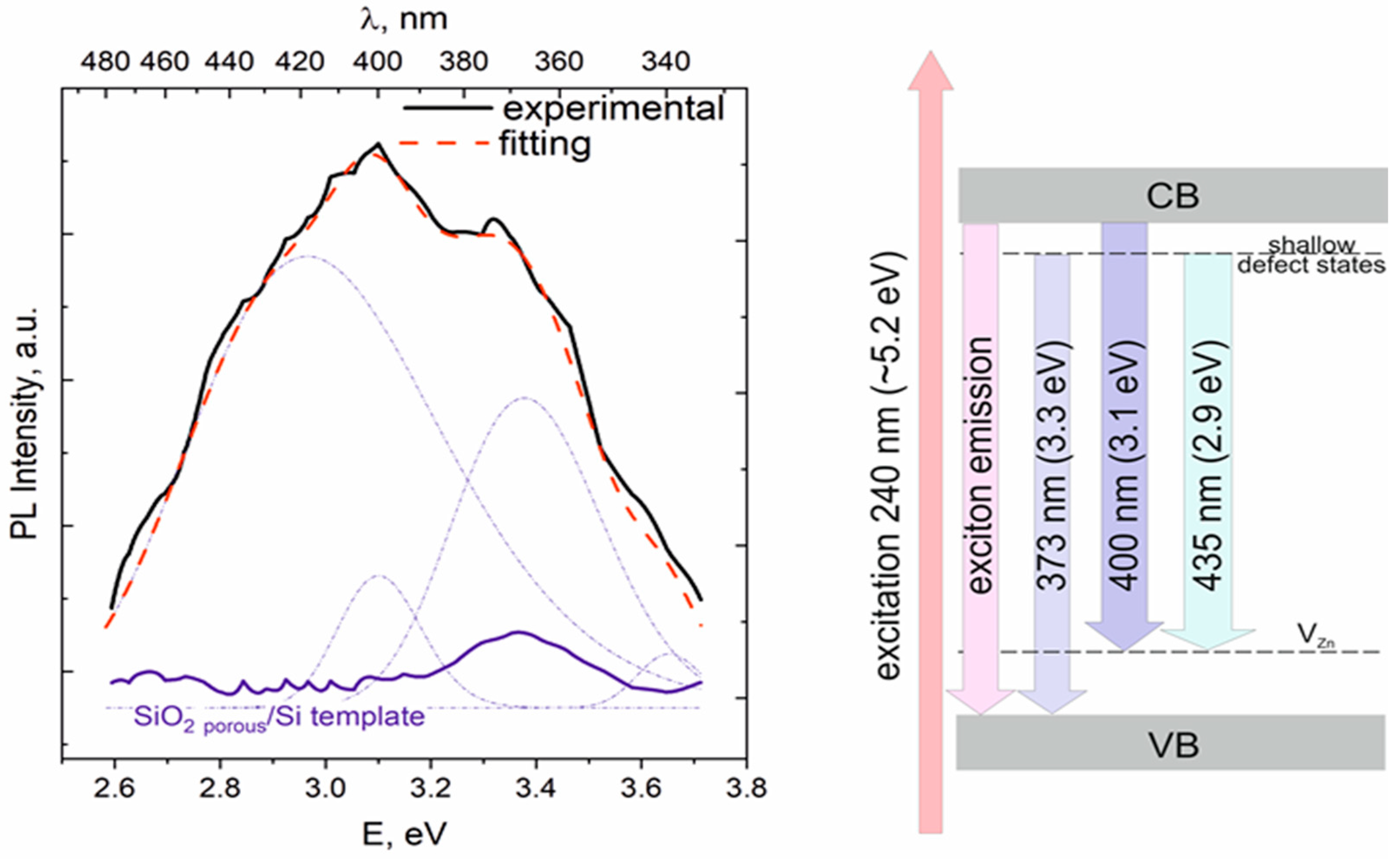
Figure 7 presents the PL spectrum of the SiO2 porous/Si template before and after ECD.
Figure 7.
PL spectra of the SiO2 porous/Si template, empty and with deposited ZnS nanocrystals, and the schematic energy level diagram.
As can be seen, the synthesized nanocrystals emit in the UV and blue range from 2.6 eV (477 nm) to 3.7 eV (335 nm). The SiO2 porous/Si template exhibits only a weak band at 3.4 eV. This band can be attributed to oxygen-related defects in amorphous SiO2 [82]. However, taking into account the absence of the characteristic emission band of amorphous SiO2 (~2.7 eV), the observed luminescence around 3.4 eV might instead originate from transitions in the crystalline Si substrate [83], which may have become partially exposed and damaged during the etching of tracks in the SiO2 layer.
The sample with filled templates exhibits a significantly more intense (approximately threefold) and broader emission band in the UV–blue spectral range. The spectrum was deconvoluted into Gaussian components in order to resolve overlapping contributions. The resulting fitting indicates that the emission band can be described by four main components centered at 340 nm (3.65 eV), 372 nm (3.3 eV), 400 nm (3.1 eV), and 420 nm (2.9 eV). The higher-energy emission observed around 3.65 eV, which is absent in the unfilled templates, indicates that the bandgap exceeds 3.4 eV, consistent with the literature values ranging from 3.5 to 3.8 eV [12]. Accordingly, this emission can be attributed to the near-band-edge recombination of free and bound excitons [84].
The lower-energy emission components are generally associated with defect-related recombination processes in ZnS. Taking into account the S-rich composition confirmed by EDX data, zinc vacancies (VZn), sulfur antisite defects (SZn) and interstitial sulphur (Si) are expected to be the dominant intrinsic defects in ZnS. According to ref. [85], VZn acts as a deep acceptor, with transition levels located 1.14 eV and 0.47 eV above the valence band (VB) for VZn2− and neutral VZn0, respectively. The sulfur antisite defect (SZn) acts as a deep donor, introducing energy levels 1.39 eV below the conduction band (CB). Sulphur interstitials introduce two levels within the bandgap: Si0 at 0.85 eV above the VB and Si2− at 0.05 eV below the CB.
Considering the excitonic emission at approximately 3.55 eV, the band at 400 nm can be attributed to intrinsic defects that introduce states (~0.45 eV), which corresponds well to the zinc vacancy level. The energy level corresponding to the PL band at 372 nm (3.3 eV) is approximately 0.2 eV, making it difficult to assign definitively to a specific intrinsic defect type. Taking into account the absence of any post-treatment of the deposited ZnS NCs and the observation of the surface optical (SO) phonon mode in the Raman spectrum, the band at 3.3 eV is more likely associated with surface-related states, which typically lie near the bottom of the conduction band [12,86]. Therefore, the emission at 372 nm is attributed to recombination holes at surface states. Finally, the emission at 435 nm (2.8 eV) is attributed to donor–acceptor pair recombination involving shallow surface defect states and zinc vacancies. These radiative transitions are illustrated in the schematic energy level diagram (Figure 6).
Thus, the contribution to the luminescence of the synthesized nanocrystals is made by both the edge luminescence in ZnS crystals as well as the recombination of charge carriers at levels of surface defects and Zn vacancies.
3.4. Brief Comparison of Optical and Structural Properties for Nanostructured ZnS and Similar Materials Created by Different Methods: Application Potential of ZnS NCs/SiO2 porous/Si Composites
We have compared the data on crystal structure, bandgap values and PL features of ZnS ensembles synthesized in our experiment with the results from the literature for ZnS thin films and nanostructures fabricated by different methods as well as for the similar binary II-VI semiconductor nanomaterials. Results of this comparison are presented in Table 3.
Table 3.
Crystal structure, bandgap and PL of some II-VI compounds synthesized by different methods.
Crystalline or polycrystalline ZnS phases are needed for most applications due to better optical and optoelectrical performances. It can be seen from Table 3 that, in order to obtain the ZnS crystalline phase using sol–gel, chemical bath or spray methods, it is necessary to carry out precipitation at an elevated temperature or to use additional annealing of deposited films. The elevated temperature during deposition can lead to an undesired oxidation of ZnS, and post-deposition annealing requires an inert environment. In our experiment, the cubic ZnS nanocrystallites were synthesized by electrochemical deposition at room temperature. It should especially mark the preferred crystallographic orientation (texture) of ZnS nanocrystals along the (220) plane. We have suggested that the use of the Si(100) substrate promoted the growth of ZnS in the (220) orientation.
The bandgap values of the of ZnS vary within fairly wide limits depending on the synthesis conditions. The most intense PL of undoped ZnS is observed in the UV–blue range regardless of the synthesis method. In particular, in our experiment, ZnS NCs/SiO2 porous/Si composite exhibits PL in the UVA–violet range, which is promising for an application in the field of UVA and violet light-emitting diodes. More precise control of the emitting properties and their enhancement could be achieved by controlling the level of defects in the ZnS bandgap (for example, via the variation in Zn/S ratio, additional annealing or by introducing proper metal impurities into the electrolyte during deposition). It should be emphasized that arrays of ZnS nanocrystals were formed directly in the SiO2/Si template, making the process fully compatible with modern CMOS technologies. This opens the way to direct integration of ZnS nanostructures into silicon chips.
ZnS is a suitable candidate for UV detection due to its wide bandgap (UV region). Though, it is difficult to realize both high responsivity and fast response speed in photodetectors based on ZnS nanostructures due to the high charge recombination rate. The way to obtain a high-performance ZnS UV photodetector is to combine the other II–VI materials (ZnO, CdS or CdSe) with ZnS to enhance the UV-light absorption and to facilitate the charge separation of photogenerated electron–hole pairs [92]. The SiO2 porous/Si matrix has been proven as a suitable template for the electrochemical deposition of the arrays of nanocrystals of II–VI materials (see Section 1). This opens up the possibility to enhance ZnS photodetector performances via obtaining composites from alternating layers of ZnS and the proper materials deposited into the SiO2 porous/Si template.
From a technological perspective, the proposed approach combines the advantages of template-assisted nanostructuring with direct compatibility with silicon-based technologies. The electrochemical deposition process is performed at room temperature and does not require high-temperature post-treatment, which is beneficial for integration into existing microelectronic fabrication routes. However, several challenges remain to be addressed before practical implementation. In particular, further optimization is required to improve the reproducibility and uniformity of pore filling over large areas, as well as to evaluate the long-term operational stability of the ZnS/SiO2/Si nanocomposites. In addition, the scalability of the ion-track template fabrication process and subsequent electrochemical deposition should be investigated in future studies aimed at device-level applications.
3.5. Electrical Properties
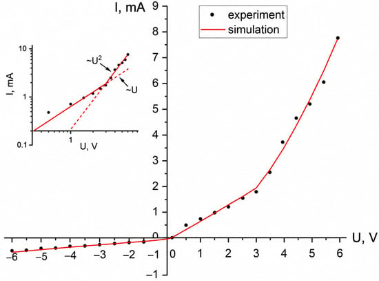
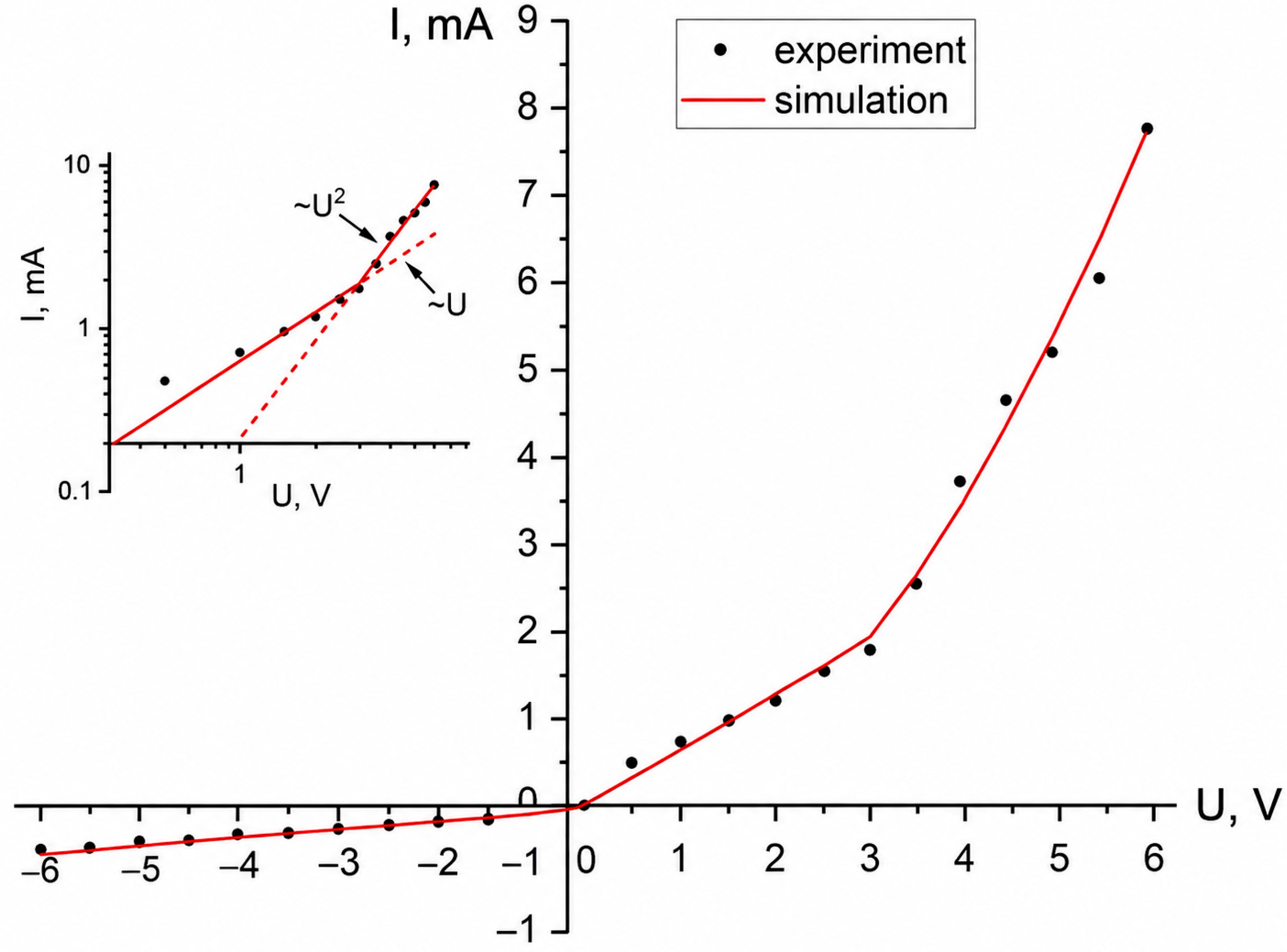
Figure 8 shows the current–voltage characteristics for the sample with deposited ZnS nanoclusters. CVC analysis reveals an electronic type of conductivity of the ZnS (NCs)/SiO2 porous/Si structure. The forward branch of the current–voltage curve of the structure at bias voltages up to UΩ ≈ 3 V is described by a linear dependence, and at higher bias voltages—by a nonlinear, but not exponential, dependence. The reverse branch of the current–voltage characteristic can be described by a linear dependence with reasonable accuracy for the entire range of applied voltages. This behavior can be explained in the framework of the space-charge-limited currents (SCLC) model.
Figure 8.
Current–voltage curve for the sample with ZnS nanocrystals after 10 min deposition. Circles—experimental data; lines—data fitting with (1–3). The inset shows a log–log plot of the forward branch of the I–V characteristic with the slope altering from I~U to I~U2.
In bulk semiconductors and dielectric materials, SCLC is typically manifested by nonlinear current–voltage characteristics, often following a quadratic dependence I ∝ U2 [93,94]. Such behavior is characteristic of mobility-controlled transport under conditions of low free-carrier density. A reduced concentration of mobile carriers may result from weak background doping, the presence of trapping centers, or contact depletion regions extending over distances comparable to or exceeding the transport channel length. As a rule, for thick ZnS films, the current–voltage characteristics in the range of bias voltages from zero to 100 V are linear [95,96]. Nonlinearities were observed in the I–V characteristics of ZnS single crystals with a thickness of d = 0.1–1 mm at higher bias voltages from 100 to 2000 V [95]. The slope of the linear forward branches of the I–V characteristics plotted in double logarithmic coordinates commonly alters from unity (I~U) to two (I~U2) at the point UΩ. Polycrystalline ZnS films produced by the close-spaced vacuum sublimation (CSVS) technique with a Mo underlayer and an In upper contact show UΩ = 15 ÷ 25 V, depending on the deposition temperature of the ZnS films [95]. In addition, current steps resulting from the occupation of deep traps in ZnS could be observed in the I–V characteristics. Current grows rapidly with I–V dependencies like I~U3–11 until all traps of similar type are filled. In studies of thin single-crystal wafers (d ≈ 5 μm), the complete occupation of traps was observed at voltages 50–100 V [92]. According to data presented in [95], the complete occupation of traps in CSVS ZnS polycrystalline films occurs at bias voltages higher than 25 V.
Nonlinear CVC is frequently observed in structures containing semiconductor nanowires and nanorods, even when the behavior cannot be attributed to Schottky contacts or tunneling barriers [97,98]. The influence of SCLC is especially pronounced in high-aspect-ratio nanostructures, where electrostatic screening is inefficient. In addition, the large surface-to-volume ratio enhances carrier depletion caused by surface states, while growth-related defects introduce numerous trapping centers, both of which favor the development of SCLC-dominated transport. We suppose that the above-mentioned method can fully apply to conical-shaped structures filled with nanoclusters with charge traps on the grain boundaries.
Thus, we will consider the direct branch of the current–voltage characteristic as consisting of two parts: the first part (U = 0 ÷~3 V) is characterized by a linear dependence I = 6.4 × 10⁻⁴ U, and the second (U = ~3 V ÷ 6 V) by a quadratic dependence I = 2.15 × 10⁻⁴ U2. The quadratic dependence was chosen as the best fit of the experimental data.
The specific conductance of whole structure containing nanocrystal arrays is calculated from the linear part of the forward branch of a I–V curve by the following formula:
where l is the length of nanocrystal arrays (approximately corresponding to the thickness of the oxide layer—520 nm); A is the contact area; and dI/dU is the differential conductance.
Therefore, the overall electrical conductivity of the structure containing ZnS nanocrystal-filled pores could be estimated as 1.11 × 10⁻⁷ Ohm−1 cm−1 for U = 0 ÷ 3 V.
The electrical conductivity of each conical nanowire composed of an array of nanocrystals was calculated using the following equation:
where Φ is the pore density (which was assumed to be equal to the ion fluence, since each incident ion was considered to produce an etchable latent track. The parameter η represents the fraction of pores completely filled with ZnS and was estimated to be 88%. The parameter r corresponds to the radius of the cylinder-shaped nanopores. Although the pores possess a conical geometry, an average radius of 165 nm was used in the calculations based on SEM observations).
The conductivity of each conical wire consisting of a ZnS nanocrystal array for low-bias voltages (U = 0 ÷ 3 V) is equal to 1.54 × 10⁻⁶ Ohm−1 cm−1.
For higher bias voltages (U = 3 ÷ 6 V), we use Lampert’s law. In the case of SCLC in a solid with shallow traps, the I–V characteristic could be described as follows [94]:
where θ << 1 is Lampert’s parameter, i.e., the ratio of the concentration of free charge carriers at the anode to the total concentration of free and trapped charge carriers, ε is the static dielectric constant of a solid, ε0 is the permittivity of free space, μ is bulk mobility, and l is the thickness of the layer.
Current density through the pores filled with nanocrystals could be expressed as follows:
Assuming that electron mobility for bulk sphalerite structured ZnS is equal to 200 cm2V−1 s−1, ε = 7.59, l = 520 nm, Lampert’s parameter θ calculated from (3) and (4) is equal to 1.78 × 10⁻².
It should be noted that, for the considered range of applied voltages, the obtained I-V characteristic does not contain a section of a sharp current increase described by I~U>2 dependency, which does not allow us to estimate the possible concentration of traps. For example, for [95]
where Nt is the density of localized states, Ucto is the voltage corresponding to complete trap occupation, and q is the electron charge.
We can only assume that, if Ucto in our case is higher than 6 V, then the corresponding density of traps should not be less than 1.86 × 1016 cm−3. In [94], some expressions were obtained for the parameters of traps with different energy distributions: uniform, Gaussian, and exponential. Without knowing the exact density of traps, we can only estimate the density of free carriers n0 in the case of all traps having the same energy level:
Assuming UΩ = 3 V, calculated n0 is equal to 9.1 × 1013 cm−3, which is significantly less than the concentration of free carriers in undoped single-crystal bulk ZnS ne = 6 × 1016 cm−3 [99]. The comparison of the conductivity of a conical wire of ZnS nanocrystals estimated from our experiment with the literature is given in Table 4.
Table 4.
Comparison of conductivity of different ZnS structures.
Thus, the conductivity of the arrays of ZnS nanocrystals embedded into the SiO2 porous/Si template is comparable with the conductivity of polycrystalline ZnS films.
3.6. DFT Calculations
According to calculations, ZnS is characterized by a sphalerite structure (space group ) with two atoms per primitive unit cell (or eight atoms per conventional unit cell). Zn2+ is bonded to four equivalent S2− atoms to form a corner-sharing ZnS4 tetrahedral. All Zn-S bond lengths are 2.37 Å. S2− is bonded to four equivalent Zn2+ atoms to form corner-sharing S-Zn4 tetrahedra. Table 5 shows the calculated lattice parameters (a), volume of a unit cell (V), density (ρ) and bandgap (Eg) of a ZnS crystal in comparison with our experimental results as well as the data from the literature. The B3LYP results overall are more accurate than PBE when compared with known experimental data, except for the bandgap, which is considerably overestimated (Table 5). This behavior can be attributed to the strong dependence of quantum-chemical calculations on the selected basis set. As reported by Oliveira et al. [60], modifications accounting for basis set incompleteness and basis set superposition error (BSSE) significantly improve the description of structural and thermochemical properties. However, the calculated electronic properties reveal that the bandgap values do not show a comparable improvement, despite the enhanced accuracy of the crystal structural parameters. Nevertheless, the predicted values remain in good agreement with the available experimental data.
Table 5.
Calculated (PBE/B3LYP) and experimental properties of ZnS in comparison with the literature data.
The Mulliken atomic charges [q(Zn) +1.32 e, q(S) = −1.32 e] and bonding population (~0.14 e) evidence a considerable covalency of the Zn−S chemical bonding.
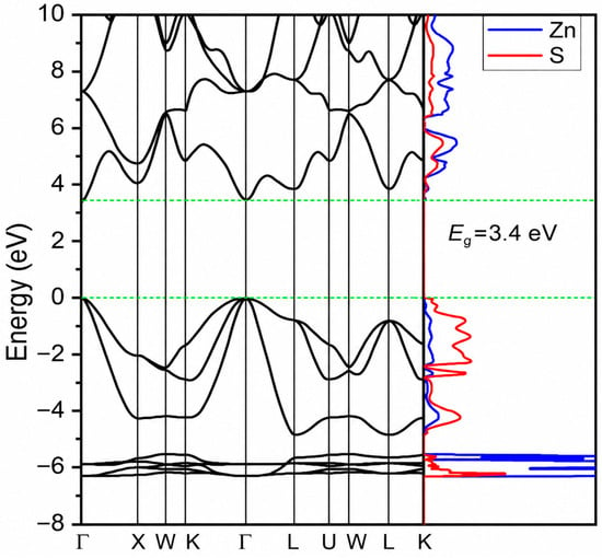
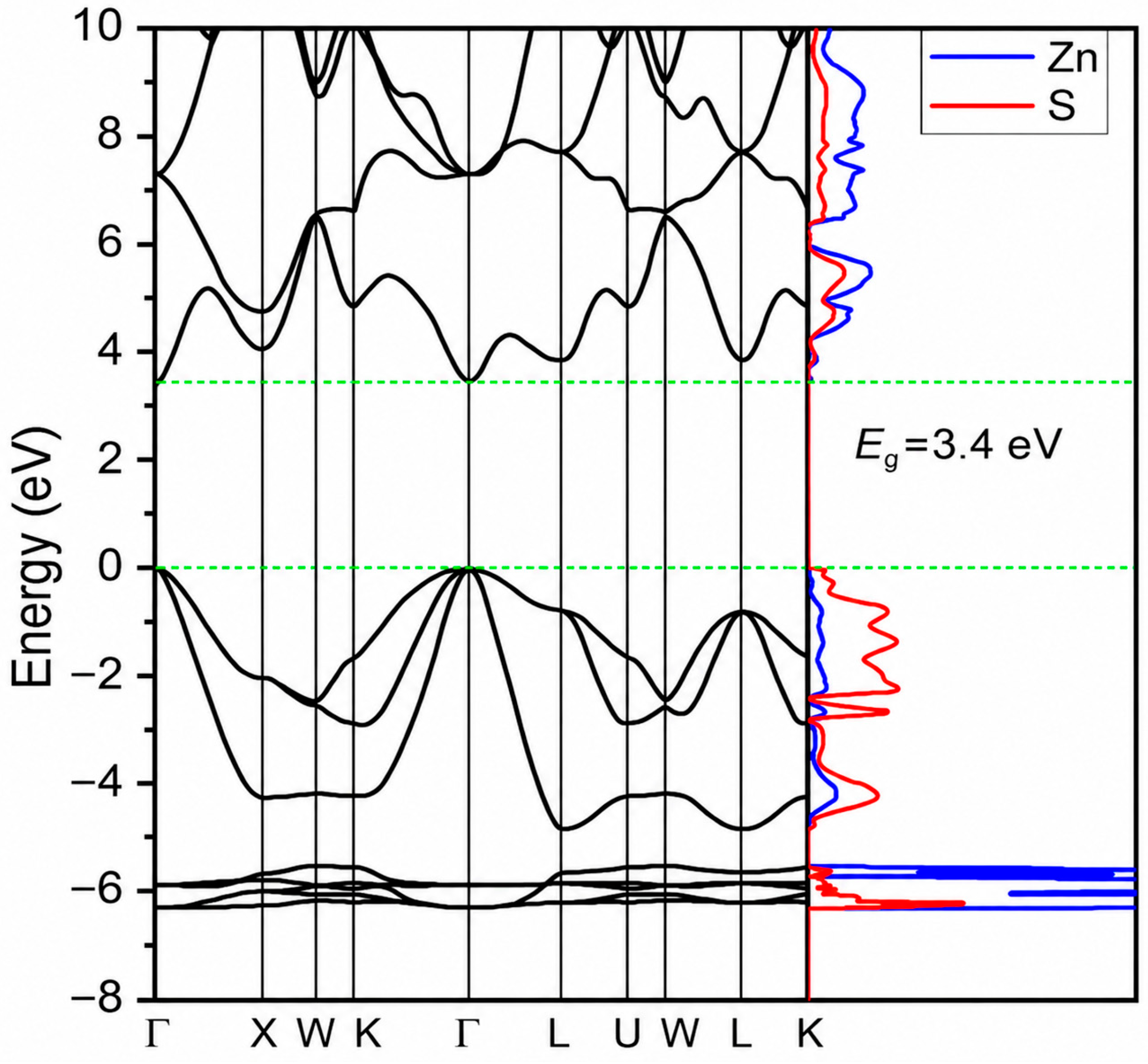
The PBE-calculated density of states and the corresponding band structure of the ZnS crystal are shown in Figure 9 (the B3LYP results are similar). The top of the valence band and the bottom of the conduction band consist mainly of the S 3p anionic states, while the bottom of the conduction band is represented by Zn 4s states hybridized with the S 3p states [103]. ZnS is a direct-gap material with a bandgap of 3.4 eV, which is in good agreement with the experimentally observed sharp onset of absorption at 3.5 eV [101]. The obtained results for ZnS are in good agreement with previous theoretical studies which used a local functions basis [77], the plane augmented wave method [78] and full potential linearized augmented plane wave (FP-LAPW) [104].
Figure 9.
ZnS band structure. Coordinates of k-points Γ = (0, 0, 0), X = (0, 1/2, 1/2), W = (1/4, 3/4, 1/2), K = (3/8, 3/4, 3/8), L = (1/2, 1/2, 1/2), U = (1/4, 5/8, 5/8). The Fermi level is at the maximum of the valence band.
4. Conclusions
For the first time, ordered arrays of ZnS nanocrystals were synthesized in SiO2/Si track templates using electrochemical deposition at room temperature. The developed approach enables the fabrication of ZnS nanoarrays directly within a silicon-compatible platform, which is attractive for future optoelectronic and sensing applications.
Structural characterization confirmed the formation of cubic ZnS nanocrystals (space group F-43m) with a preferred (220) orientation and an average crystallite size of approximately 4.2 nm. The pore filling degree reached about 88%, while the lattice parameter of ZnS was determined to be 5.62 Å. The obtained nanocomposites exhibited intense ultraviolet–blue photoluminescence in the range of 335–477 nm with dominant emission peaks at 372 nm (3.3 eV) and 400 nm (3.1 eV), whereas the estimated bandgap was 3.4–3.6 eV. Electrical measurements revealed predominantly electronic conductivity, and the current–voltage characteristics were successfully described within the space-charge-limited current model. The conductivity of the ZnS nanoarrays was estimated to be 1.54 × 10⁻⁶ Ω−1·cm−1, which is comparable to values reported for polycrystalline ZnS films.
Density functional theory calculations provided additional insight into the electronic structure of ZnS and yielded a bandgap value in good agreement with available experimental data. Although the theoretical analysis was primarily used to support the experimental observations, the obtained results are consistent with the expected electronic properties of ZnS.
Overall, the results demonstrate that SiO2/Si track templates represent a promising platform for the controlled growth of ZnS nanocrystal arrays. The combination of structural ordering, optical activity, and compatibility with silicon technology makes these nanocomposites attractive for further development of ultraviolet photodetectors, optoelectronic components, and sensing devices.
Author Contributions
Conceptualization, A.A. and E.P.; methodology, A.U. and A.T.A.; software, V.Y.; investigation, A.A., I.P., A.T.T. and M.A.; formal analysis, L.A.V. and M.A.; resources, L.A.V. and S.M.; data curation, A.A. and E.P.; writing—original draft preparation, A.A. and L.A.V.; funding, A.A., A.I.P. and M.K.; writing—review and editing, A.A., A.I.P., E.P. and M.K. All authors have read and agreed to the published version of the manuscript.
Funding
A.I. Popov, E. Popova, and M. Konuhova gratefully acknowledge partial support from the HORIZON-MSCA-2025-SE-01 project, Project No. 101299799, “Post-irradiation Multiscale Dynamics of Materials” (PRISMA).
Institutional Review Board Statement
Not applicable.
Informed Consent Statement
Not applicable.
Data Availability Statement
The raw data supporting the conclusions of this article will be made available by the authors on request.
Acknowledgments
This work was partly supported by the Belarusian state program of scientific research ‘Photonics and electronic for innovations’ (projects 3.8.1, SR No 20212595).
Conflicts of Interest
The authors declare no conflicts of interest.
References
- Chatterjee, A.; Kumar, G.K.; Roymahapatra, G.; Das, H.S.; Jaishree, G.; Rao, T.S. Zinc chalcogenide nanostructures: Synthesis, methodologies and applications. Front. Nanotechnol. 2024, 6, 1433591. [Google Scholar] [CrossRef] [Scilit]
- Ando, M.; Kawasaki, H.; Tamura, S.; Haramoto, Y.; Shigeri, Y. Recent Advances in Gas Sensing Technology Using Non-Oxide II-VI Semiconductors CdS, CdSe, and CdTe. Chemosensors 2022, 10, 482. [Google Scholar] [CrossRef] [Scilit]
- Lu, X.; Wang, Z.; Wang, J.; Li, Y.; Hou, X. Ultrasensitive fluorescence detection of ascorbic acid using silver ion-modulated high-quality CdSe/CdS/ZnS quantum dots. ACS Omega 2024, 9, 27127–27136. [Google Scholar] [CrossRef] [Scilit] [PubMed]
- Lamonova, K.; Prokhorov, A.; Schmidbauer, M.; Kwasniewski, A.; Kazarinov, Y.; Konuhova, M.; Platonenko, A.; Remeš, Z.; Ridžonov, K.; Buryi, M. Luminescence properties of ZnSe single crystals co-doped with Fe and Cr. Opt. Mater. X 2025, 25, 100393. [Google Scholar] [CrossRef] [Scilit]
- Bolatov, A.; Manjovelo, A.; Chouchene, B.; Balan, L.; Gries, T.; Medjahdi, G.; Uralbekov, B.; Schneider, R. Ternary ZnS/ZnO/Graphitic Carbon Nitride Heterojunction for Photocatalytic Hydrogen Production. Materials 2024, 17, 4877. [Google Scholar] [CrossRef] [Scilit] [PubMed]
- Suchikova, Y.; Kovachov, S.; Bohdanov, I.; Popova, E.; Moskina, A.; Popov, A. Characterization of CdxTeyOz/CdS/ZnO Heterostructures Synthesized by the SILAR Method. Coatings 2023, 13, 639. [Google Scholar] [CrossRef] [Scilit]
- Burashev, G.; Tatykayev, B.; Baláž, M.; Khan, N.; Seysembekova, A.; Tugelbay, S.; Turgynbay, N.; Burkitbayev, M.; Shalabayev, Z. All solid-state fabrication strategy of CdS@ZnS nanocomposites and their photocatalytic performance in water purification. Int. J. Biol. Chem. 2023, 16, 110–122. [Google Scholar] [CrossRef] [Scilit]
- Chakrabarti, A.; Alessandri, E. Syntheses, Properties, and Applications of ZnS-Based Nanomaterials. Appl. Nano 2024, 5, 116–142. [Google Scholar] [CrossRef] [Scilit]
- Degoda, V.; Doroshenko, I.; Kogut, Y.; Podust, H.; Pavlova, N. Influence of excitation nature on temperature attenuation of luminescence in ZnSe crystals. Results Opt. 2022, 9, 100286. [Google Scholar] [CrossRef] [Scilit]
- Dile, M.; Laganovska, K.; Zolotarjovs, A.; Bite, I.; Vanags, E.; Pudza, I.; Kuzmin, A.; Smits, K. The effect of surfactants and precursors on the structure and properties of ZnS:Cu nanocrystalline particles. Nanostruct. Nano-Objects 2023, 35, 101023. [Google Scholar] [CrossRef] [Scilit]
- Reshak, A.H.; Auluck, S.; Piasecki, M.; Myronchuk, G.L.; Parasyuk, O.; Kityk, I.V.; Kamarudin, H. Absorption and photoconductivity spectra of Ag2GeS3 crystal: Experiment and theory. Spectrochim. Acta Part A Mol. Biomol. Spectrosc. 2012, 93, 274–279. [Google Scholar] [CrossRef] [Scilit] [PubMed]
- Jubeer, E.M.; Manthramme, M.A.; Subha, P.A.; Shkir, M.; Biju, K.P.; AlFaify, S.A. Defect engineering for enhanced optical and photocatalytic properties of ZnS nanoparticles synthesized by hydrothermal method. Sci. Rep. 2023, 13, 16820. [Google Scholar] [CrossRef] [Scilit] [PubMed]
- Fang, X.; Zhai, T.; Gautam, U.K.; Li, L.; Wu, L.; Bando, Y.; Golberg, D. ZnS nanostructures: From synthesis to applications. Prog. Mater. Sci. 2011, 56, 175–287. [Google Scholar] [CrossRef] [Scilit]
- Wang, L.X.; Huang, H.; Liang, B.; Liu, Z.; Chen, D.; Shen, G. ZnS Nanostructures: Synthesis, Properties, and Applications. Crit. Rev. Solid State Mater. Sci. 2013, 38, 57–90. [Google Scholar] [CrossRef] [Scilit]
- Anand, K.V.; Chinnu, M.K.; Kumar, R.M.; Mohan, R.; Jayavel, R. Formation of zinc sulfide nanoparticles in HMTA matrix. Appl. Surf. Sci. 2009, 255, 8879–8882. [Google Scholar] [CrossRef] [Scilit]
- Kumari, P.; Sharma, A.; Kumawat, A.; Samanta, S.; Misra, K.P.; Rao, A.; Kabi, S.; Chattopadhyay, S. Strong UV emission in flakes-like ZnS nanoparticles synthesized by cost effective sol-gel method. Mater. Today Proc. 2022, 58, 642–647. [Google Scholar] [CrossRef] [Scilit]
- Okamoto, N.; Matsuda, N.; Saito, T. Electrodeposition of ZnS and evaluation of its electrochemical property. Jpn. J. Appl. Phys. 2022, 61, SC1075. [Google Scholar] [CrossRef] [Scilit]
- Tonelli, D.; Scavetta, E.; Gualandi, I. Electrochemical Deposition of Nanomaterials for Electrochemical Sensing. Sensors 2019, 19, 1186. [Google Scholar] [CrossRef] [Scilit] [PubMed]
- Grier, D.; Ben-Jacob, E.; Clarke, R.; Sander, L.M. Morphology and microstructure in electrochemical deposition of zinc. Phys. Rev. Lett. 1986, 56, 1264–1267. [Google Scholar] [CrossRef] [Scilit] [PubMed]
- Hussain, S.; Erikson, H.; Kongi, N.; Merisalu, M.; Rähn, M.; Sammelselg, V.; Maia, G.; Tammeveski, K. Platinum particles electrochemically deposited on multiwalled carbon nanotubes for oxygen reduction reaction in acid media. J. Electrochem. Soc. 2017, 164, F1014. [Google Scholar] [CrossRef] [Scilit]
- Linge, J.M.; Erikson, H.; Kozlova, J.; Sammelselg, V.; Tammeveski, K. Oxygen reduction reaction on electrochemically deposited silver nanoparticles from non-aqueous solution. J. Electroanal. Chem. 2018, 810, 129–134. [Google Scholar] [CrossRef] [Scilit]
- Shah, S.S.; Das, H.T.; Barai, H.R.; Aziz, M.A. Boosting the electrochemical performance of polyaniline by one-step electrochemical deposition on nickel foam for high-performance asymmetric supercapacitor. Polymers 2022, 14, 270. [Google Scholar] [CrossRef] [Scilit] [PubMed]
- Shypunov, I.; Kongi, N.; Kozlova, J.; Matisen, L.; Ritslaid, P.; Sammelselg, V.; Tammeveski, K. Enhanced oxygen reduction reaction activity with electrodeposited Ag on manganese oxide–graphene supported electrocatalyst. Electrocatalysis 2015, 6, 465–471. [Google Scholar] [CrossRef] [Scilit]
- Pikalova, E.; Osinkin, D.; Kalinina, E. Direct Electrophoretic Deposition and Characterization of Thin-Film Membranes Based on Doped BaCeO3 and CeO2 for Anode-Supported Solid Oxide Fuel Cells. Membranes 2022, 12, 682. [Google Scholar] [CrossRef] [Scilit] [PubMed]
- Osinkin, D.A.; Zakharov, D.M.; Khodimchuk, A.V.; Antonova, E.P.; Bogdanovich, N.M.; Gordeev, E.V.; Suntsov, A.Y.; Porotnikova, N.M. Strategy for improving the functional performances of complex oxide through the use of a fluorine-containing precursor. Int. J. Hydrogen Energy 2023, 48, 22624–22633. [Google Scholar] [CrossRef] [Scilit]
- Osinkin, D.A.; Antonova, E.P.; Porotnikova, N.M.; Bogdanovich, N.M. Features of the electrochemical reaction of hydrogen oxidation on the composite SrFeO3-based anode for a protonic ceramic fuel cell. Int. J. Energy Res. 2022, 46, 12597–12607. [Google Scholar] [CrossRef] [Scilit]
- Kotelnikova, A.; Kadyrzhanov, K.; Shlimas, D.; Trukhanov, A.; Shakirzyanov, R.; Zubar, T.; Zdorovets, M.; Osmanova, S.; Huseynov, H.; Hashimov, R. Optimization of the electrochemical deposition method for preparation magnetic non-magnetic multilayered structures. Adv. Phys. Res. 2025, 7, 273–280. [Google Scholar] [CrossRef] [Scilit]
- Bograchev, D.A.; Kabanova, T.B.; Davydov, A.D. Electrodeposition of metals into nano/micropores of templates: A type of electrochemistry under confinement. J. Solid State Electrochem. 2025, 29, 1309–1340. [Google Scholar] [CrossRef] [Scilit]
- Dai, Q.; Liu, L.; Wang, P.; Wu, X.; Huang, Z.; Zhu, J.; Tian, J. Highly ordered ZnS nanowire arrays embedded in anodic alumina membrane by a hydrothermal method with double diffusion. Mater. Lett. 2013, 107, 333–336. [Google Scholar] [CrossRef] [Scilit]
- Podhorska, L.; Delcassian, D.; Goode, A.E.; Agyei, M.; McComb, D.W.; Ryan, M.P.; Dunlop, I.E. Mechanisms of polymer-templated nanoparticle synthesis: Contrasting ZnS and Au. Langmuir 2016, 32, 9216–9222. [Google Scholar] [CrossRef] [Scilit] [PubMed]
- Kaniukov, E.Y.; Ustarroz, J.; Yakimchuk, D.V.; Petrova, M.; Terryn, H.; Sivakov, V.; Petrov, A.V. Tunable nanoporous silicon oxide templates by swift heavy ion tracks technology. Nanotechnology 2016, 27, 115305. [Google Scholar] [CrossRef] [Scilit] [PubMed]
- Demyanov, E.; Kaniukov, Y.E.; Petrov, A.V.; Belonogov, E.K.; Streltsov, E.A.; Ivanov, D.K.; Ivanova, Y.A.; Trautmann, C.; Terryn, H.; Petrova, M. On the morphology of Si/SiO2/Ni nanostructures with swift heavy ion tracks in silicon oxide. J. Surf. Investig. X-Ray Synchrotron Neutron Tech. 2014, 8, 805–813. [Google Scholar] [CrossRef] [Scilit]
- Yakimchuk, D.; Kaniukov, E.; Bundyukova, V.; Osminkina, L.; Teichert, S.; Demyanov, S.; Sivakov, V. Silver nanostructures evolution in porous SiO2/p-Si matrices for wide wavelength surface enhanced Raman scattering applications. MRS Commun. 2018, 8, 95–99. [Google Scholar] [CrossRef] [Scilit]
- Kaniukov, E.; Yakimchuk, D.; Arzumanyan, G.; Terryn, H.; Baert, K.; Kozlovskiy, A.; Zdorovets, M.; Belonogov, E.; Demyanov, S. Growth mechanisms of spatially separated copper dendrites in pores of a SiO2 template. Philos. Mag. 2017, 97, 2268–2283. [Google Scholar] [CrossRef] [Scilit]
- Osminkina, L.A.; Žukovskaja, O.; Agafilushkina, S.N.; Kaniukov, E.; Stranik, O.; Gonchar, K.A.; Yakimchuk, D.; Bundyukova, V.; Chermoshentsev, D.A.; Dyakov, S.A.; et al. Gold nanoflowers grown in a porous Si/SiO2 matrix: The fabrication process and plasmonic properties. Appl. Surf. Sci. 2020, 507, 144989. [Google Scholar] [CrossRef] [Scilit]
- Koltunowicz, T.N.; Zhukowski, P.; Fedotova, J.A.; Bayev, V.G.; Streltsov, E.A.; Baran, L.V. Electrochemically Deposited Cobalt Nanoarrays in SiO2/n-Si, Templates Produced by Swift Heavy Ion-Induced Modification Technology. Acta Phys. Pol. A 2013, 123, 929–931. [Google Scholar] [CrossRef] [Scilit]
- Giniyatova, S.; Dauletbekova, A.; Baimukhanov, Z.; Vlasukova, L.; Akilbekov, A.; Usseinov, A.; Kozlovskiy, A.; Akylbekova, A. Structure, electrical properties and luminescence of ZnO nanocrystals deposited in SiO2/Si track templates. Radiat. Meas. 2019, 125, 52–56. [Google Scholar] [CrossRef] [Scilit]
- Dauletbekova, A.; Junisbekova, D.; Baimukhanov, Z.; Kareiva, A.; Popov, A.I.; Platonenko, A.; Akilbekov, A.; Abdrakhmetova, A.; Aralbayeva, G.; Koishybayeva, Z. Synthesis and Study of Oxide Semiconductor Nanoheterostructures in SiO2/Si Track Template. Crystals 2024, 14, 1087. [Google Scholar] [CrossRef] [Scilit]
- Akylbekova, A.; Dauletbekova, A.; Baimukhanov, Z.; Vlasukova, L.A.; Usseinov, A.; Saduova, N.; Akilbekov, A.T.; Pankratov, V.A.; Popov, A.I. Annealing Effect on Structural, Optical and Electrophysical Properties of ZnSe Nanocrystals Synthesized into SiO2/Si Ion Track Template. Materials 2024, 17, 4149. [Google Scholar] [CrossRef] [Scilit] [PubMed]
- Dauletbekova, A.; Akylbekova, A.; Sarsekhan, G.; Usseinov, A.; Baimukhanov, Z.; Kozlovskiy, A.; Vlasukova, L.A.; Komarov, F.F.; Popov, A.I.; Akilbekov, A.T. Ion-Track Template Synthesis and Characterization of ZnSeO3 Nanocrystals. Crystals 2022, 12, 817. [Google Scholar] [CrossRef] [Scilit]
- Ivanou, D.K.; Streltsov, E.A.; Fedotov, A.K.; Mazanik, A.V.; Fink, D.; Petrov, A. Electrochemical deposition of PbSe and CdTe nanoparticles onto p-Si (100) wafers and into nanopores in SiO2/Si (100) structure. Thin Solid Films 2005, 490, 154–160. [Google Scholar] [CrossRef] [Scilit]
- Balakhayeva, R.; Akilbekov, A.; Baimukhanov, Z.; Usseinov, A.; Giniyatova, S.; Zdorovets, M.; Vlasukova, L.; Popov, A.; Dauletbekova, A. CdTe Nanocrystal Synthesis in SiO2/Si Ion-Track Template: The Study of Electronic and Structural Properties. Phys. Status Solidi A Appl. Mater. Sci. 2021, 218, 2000231. [Google Scholar] [CrossRef] [Scilit]
- Akilbekov, A.; Balakhayeva, R.; Zdorovets, M.; Baymukhanov, Z.; Komarov, F.F.; Karim, K.; Popov, A.I.; Dauletbekova, A. Ion track template technology for fabrication of CdTe and CdO nanocrystals. Nucl. Instrum. Methods Phys. Res. Sect. B Beam Interact. Mater. At. 2020, 481, 30–34. [Google Scholar] [CrossRef] [Scilit]
- Akylbekova, A.; Mantiyeva, K.; Dauletbekova, A.; Akilbekov, A.; Baimukhanov, Z.; Vlasukova, L.; Aralbayeva, G.; Abdrakhmetova, A.; Bazarbek, A.-D.; Abdihalikova, F. The Synthesis and Characterization of CdS Nanostructures Using a SiO2/Si Ion-Track Template. Crystals 2024, 14, 1091. [Google Scholar] [CrossRef] [Scilit]
- Schwartz, K.; Maniks, J.; Manika, I. A review of colour center and nanostructure creation in LiF under heavy ion irradiation. Phys. Scr. 2015, 90, 094011. [Google Scholar] [CrossRef] [Scilit]
- Zdorovets, M.V.; Kozlovskiy, A.A.; Moldabayeva, G.Z.; Ivanov, I.A.; Konuhova, M. Radiation-induced degradation effects of optical properties of MgO ceramics caused by heavy ion irradiation. Opt. Mater. X 2025, 26, 100406. [Google Scholar] [CrossRef] [Scilit]
- Kozlovskiy, A.L.; Akhmetzhan, S.; Ivanitskaya, N.; Kenzhina, I.E.; Zdorovets, M.V. Study of the effect of irradiation with Ca5+ ions on the increase in Ni nanotubes lifetime applicable as the basis for lithium-ion batteries. Mater. Res. Express 2019, 6, 085074. [Google Scholar] [CrossRef] [Scilit]
- Karipbayev, Z.T.; Kumarbekov, K.; Manika, I.; Dauletbekova, A.; Kozlovskiy, A.L.; Sugak, D.; Ubizskii, S.B.; Akilbekov, A.; Suchikova, Y.; Popov, A.I. Optical, Structural, and Mechanical Properties of Gd3Ga5O12 Single Crystals Irradiated with 84Kr+ Ions. Phys. Status Solidi B Basic Solid State Phys. 2022, 259, 2100415. [Google Scholar] [CrossRef] [Scilit]
- Kozlovskiy, A.L.; Ryskulov, A.E.; Ivanov, I.A.; Zhumakhanova, G.; Popov, A.; Konuhova, M. Determination of the influence of temperature factors on the softening of the near-surface layer of BeO ceramics under high-dose irradiation with helium ions. Eurasian J. Phys. Funct. Mater. 2025, 9, 71–78. [Google Scholar] [CrossRef] [Scilit]
- Kutuzau, M.; Kozlovskiy, A.; Borgekov, D.; Kenzhina, I.; Zdorovets, M.; Chernik, A.; Alisienok, O.; Shumskaya, A.; Kaniukov, E. Optimization of PET ion-track membranes parameters. Mater. Today Proc. 2019, 7, 866–871. [Google Scholar] [CrossRef] [Scilit]
- Kozlovskiy, A.L.; Alin, M.; Borgekov, D.B. Study of Polymorphic Transformation Processes and Their Influence in Polycrystalline ZrO2 Ceramics upon Irradiation with Heavy Ions. Ceramics 2023, 6, 686–706. [Google Scholar] [CrossRef] [Scilit]
- Assylbayev, R.; Tursumbayeva, G.; Baubekova, G.; Karipbayev, Z.T.; Krasnikov, A.; Shablonin, E.; Aralbayeva, G.M.; Smortsova, Y.; Akilbekov, A.; Popov, A.I.; et al. Influence of Energetic Xe132 Ion Irradiation on Optical, Luminescent and Structural Properties of Ce-Doped Y3Al5O12 Single Crystals. Crystals 2025, 15, 683. [Google Scholar] [CrossRef] [Scilit]
- Benyagoub, A.; Toulemonde, M. Ion Tracks in Amorphous Silica. J. Mater. Res. 2015, 30, 1529–1543. [Google Scholar] [CrossRef] [Scilit]
- Komarov, F.F. Nano- and Microstructuring of Solids by Swift Heavy Ions. Phys.–Uspekhi 2017, 60, 435–471. [Google Scholar] [CrossRef] [Scilit]
- Dallanora, A.; Marcondes, T.L.; Bermudez, G.G.; Fichtner, P.F.P.; Trautmann, C.; Toulemonde, M.; Papaléo, R.M. Nanoporous SiO2/Si thin layers produced by ion track etching: Dependence on the ion energy and criterion for etchability. J. Appl. Phys. 2008, 104, 024307. [Google Scholar] [CrossRef] [Scilit]
- Zicovich-Wilson, C.M.; Dovesi, R. On the Use of Symmetry-Adapted Crystalline Orbitals in SCF-LCAO Periodic Calculations. I. The Construction of the Symmetrized Orbitals. Int. J. Quantum Chem. 1998, 67, 299–309. [Google Scholar] [CrossRef] [Scilit]
- Zicovich-Wilson, C.M.; Dovesi, R. On the use of symmetry-adapted crystalline orbitals in SCF-LCAO periodic calculations. II. Implementation of the self-consistent-field scheme and examples. Int. J. Quantum Chem. 1998, 67, 311–320. [Google Scholar] [CrossRef]
- Dovesi, R.; Erba, A.; Orlando, R.; Zicovich-Wilson, C.M.; Civalleri, B.; Maschio, L.; Rérat, M.; Casassa, S.; Baima, J.; Salustro, S.; et al. Quantum-mechanical condensed matter simulations with CRYSTAL. Wiley Interdiscip. Rev. Comput. Mol. Sci. 2018, 8, e1360. [Google Scholar] [CrossRef] [Scilit]
- Perdew, J.P.; Burke, K.; Ernzerhof, M. Generalized Gradient Approximation Made Simple. Phys. Rev. Lett. 1996, 77, 3865. [Google Scholar] [CrossRef] [Scilit] [PubMed]
- Vilela Oliveira, D.; Laun, J.; Peintinger, M.F.; Bredow, T. BSSE-correction scheme for consistent gaussian basis sets of double- and triple-zeta valence with polarization quality for solid-state calculations. J. Comput. Chem. 2019, 40, 2364–2376. [Google Scholar] [CrossRef] [Scilit] [PubMed]
- Mulliken, R.S. Electronic population analysis on LCAO-MO molecular wave functions. II. Overlap populations, bond orders, and covalent bond energies. J. Chem. Phys. 1995, 23, 1841–1846. [Google Scholar] [CrossRef] [Scilit]
- Monkhorst, H.J.; Pack, J.D. Special points for Brillouin-zone integrations. Phys. Rev. 1976, 13, 5188–5192. [Google Scholar] [CrossRef] [Scilit]
- Adachi, S. Cubic Zinc Sulphide (β-ZnS). In Optical Constants of Crystalline and Amorphous Semiconductors; Springer: Boston, MA, USA, 1999; pp. 445–458. [Google Scholar] [CrossRef] [Scilit]
- Liu, C.H.; Yokoyama, M.; Su, Y.K.; Lee, N.C. Self-limiting growth of ZnS on Si substrates at a growth rate of 0.7 monolayers per operating cycle by atomic layer epitaxy using MOCVD. J. Soc. Inf. Disp. 1997, 5, 99–102. [Google Scholar] [CrossRef] [Scilit]
- Valkonen, M.P.; Lindroos, S.; Resch, R.; Leskela, M.; Friedbacher, G.; Grasserbauer, M. Growth of zinc sulfide thin films on 100 Si with the successive ionic layer adsorption and reaction method studied by atomic force microscopy. Appl. Surf. Sci. 1998, 136, 131–136. [Google Scholar] [CrossRef] [Scilit]
- Wang, H.Y.; Wang, C.R.; Xu, J.; Liu, X.; Xu, X.F.; Xing, H.Z.; Zhao, L.J.; Chen, X.S. Different temperature dependence of excitonic and defect-related photoluminescence spectra in ZnS nanobelts and nanowires. J. Phys. D Appl. Phys. 2012, 45, 095301. [Google Scholar] [CrossRef] [Scilit]
- Eissa, D.; Hegab, R.H.; Abou-Shady, A.; Kotp, Y.H. Green synthesis of ZnO, MgO and SiO2 nanoparticles and its effect on irrigation water, soil properties, and Origanum majorana productivity. Sci. Rep. 2022, 12, 5780. [Google Scholar] [CrossRef] [Scilit] [PubMed]
- Lin, M.-H.; Ho, C.-H. Synthesis and Optical Characterization of Oxygen-Incorporated ZnS(1-x)Ox for UV-Visible Color Palette Light-Emission Matter. ACS Omega 2017, 2, 4514–4523. [Google Scholar] [CrossRef] [Scilit] [PubMed]
- Ureña, F.; Olsen, S.H.; Raskin, J.-P. Raman measurements of uniaxial strain in silicon nanostructures. J. Appl. Phys. 2013, 114, 144507. [Google Scholar] [CrossRef] [Scilit]
- Yaoa, L.D.; Wang, F.F.; Shena, X.; Youa, S.J.; Yanga, L.X.; Jiang, S.; Li, Y.C.; Zhua, K.; Liua, Y.L.; Pan, A.L.; et al. Structural stability and Raman scattering of ZnSe nanoribbons under high pressure. J. Alloys Compd. 2009, 480, 798–801. [Google Scholar] [CrossRef] [Scilit]
- Cortijo-Campos, S.; Kung, P.; Prieto, C.; de Andrés, A. Forbidden and Second-Order Phonons in Raman Spectra of Single and Few-Layer MoS2 Close to C Exciton Resonance. J. Phys. Chem. C 2021, 125, 23904–23910. [Google Scholar] [CrossRef] [Scilit]
- Kaur, P.; Kumar, S.; Singh, A.; Chen, C.L.; Dong, C.L.; Chan, T.S.; Lee, K.P.; Srivastava, C.; Rao, S.M.; Wu, M.K. Investigations on doping induced changes in structural, electronic structure and magnetic behavior of spintronic Cr–ZnS nanoparticles. Superlattices Microstruct. 2015, 83, 785–795. [Google Scholar] [CrossRef] [Scilit]
- Offor, P.O.; Ude, S.N.; Whyte, G.M.; Otung, F.U.; Madiba, I.G.; Bashir, A.; Thovhogi, N.; Okorie, B.A.; Ezema, F.I. Effect of concentration of trisodium citrate complexing agent on spraysynthesized ZnS thin films. Mater. Today Proc. 2021, 36, 133–140. [Google Scholar] [CrossRef] [Scilit]
- Synnott, D.W.; Seery, M.K.; Hinder, S.J.; Colreavy, J.; Pillai, S.C. Novel Microwave Assisted Synthesis of ZnS Nanomaterials. Nanotechnology 2013, 24, 045704. [Google Scholar] [CrossRef] [Scilit] [PubMed]
- Ho, C.-H.; Varadhan, P.; Wang, H.-H.; Chen, C.-Y.; Fang, X.; He, J.-H. Raman selection rule for surface optical phonons in ZnS nanobelts. Nanoscale 2016, 8, 5954–5958. [Google Scholar] [CrossRef] [Scilit] [PubMed]
- Serrano, J.; Cantarero, A.; Cardona, M.; Garro, N.; Lauck, R.; Tallman, R.E.; Ritter, T.M.; Weinstein, B.A. Raman scattering in β-ZnS. Phys. Rev. B 2004, 69, 014301. [Google Scholar] [CrossRef] [Scilit]
- Göde, F. Annealing temperature effect on the structural, optical and electrical properties of ZnS thin films. Phys. B Condens. Matter 2011, 406, 1653–1659. [Google Scholar] [CrossRef] [Scilit]
- Cheng, Y.C.; Jin, C.Q.; Gao, F.; Wu, X.L.; Zhong, W.; Li, S.H.; Chu, K. Raman scattering study of zinc blende and wurtzite ZnS. J. Appl. Phys. 2009, 106, 123505. [Google Scholar] [CrossRef] [Scilit]
- Komarov, F.; Vlasukova, L.; Parkhomenko, I.; Milchanin, O.; Mudryi, A.; Togambaeva, A.; Korolik, O. Raman study of light-emitting SiNx films grown on Si by low-pressure chemical vapor deposition. Thin Solid Films 2015, 579, 110–115. [Google Scholar] [CrossRef] [Scilit]
- Deshmukh, S.G.; Jariwala, A.; Agarwal, A.; Patel, C.; Panchal, A.K.; Kheraj, V. ZnS Nanostructured Thin-Films Deposited by Successive Ionic Layer Adsorption and Reaction. AIP Conf. Proc. 2016, 1724, 020033. [Google Scholar] [CrossRef] [Scilit]
- Lin, M.; Sudhiranjan, T.; Boothroyd, C.; Loh, K.P. Influence of Au catalyst on the growth of ZnS nanowires. Chem. Phys. Lett. 2004, 400, 175–178. [Google Scholar] [CrossRef] [Scilit]
- Salh, R. Defect Related Luminescence in Silicon Dioxide Network: A Review. In Crystalline Silicon—Properties and Uses; InTech: Rijeka, Croatia, 2011; pp. 135–172. [Google Scholar] [CrossRef] [Scilit] [PubMed]
- Young, A.P.; Schäfer, J.; Jessen, G.H.; Bandhu, R.; Brillson, L.J.; Lucovsky, G.; Niimi, H. Luminescence measurements of sub-oxide band-tail and Si dangling bond states at ultrathin interfaces. AIP Conf. Proc. 1998, 449, 293–297. [Google Scholar] [CrossRef] [Scilit]
- Mosquera, E.; Carvajal, N. Low temperature synthesis and blue photoluminescence of ZnS submicronparticles. Mater. Lett. 2014, 129, 8–11. [Google Scholar] [CrossRef] [Scilit]
- Hoang, K.; Latouche, C.; Jobic, S. Defect energy levels and persistent luminescence in Cu-doped ZnS, Comput. Comput. Mater. Sci. 2019, 163, 63–67. [Google Scholar] [CrossRef] [Scilit]
- Hafeez, M.; Al-Asbahi, B.A.; Jumali, M.H.H.; Yahaya, M.; Inam, F.; Bhopal, M.F.; Bhatti, A.S. Critical role of defect states on visible luminescence from ZnS nanostructures doped with Au, Mn and Ga. Mater. Sci. Semicond. Process. 2020, 117, 105193. [Google Scholar] [CrossRef] [Scilit]
- Kumar, S.; Bakshi, S.; Chaudhary, S.; Kaur, J.; Agrawal, A.P.; Rani, S. Heat post-treatment effect on optical and electrical properties of ZnS thin films. Biointerface Res. Appl. Chem. 2024, 14, 100. [Google Scholar] [CrossRef] [Scilit]
- Tounsi, A.; Khalfi, R.; Talantikite-Touati, D.; Merzouk, H.; Souici, A. Characterization of cerium-doped zinc sulfide thin films synthesized by sol–gel method. Appl. Phys. A 2022, 128, 280. [Google Scholar] [CrossRef] [Scilit]
- Islam, M.A.; Hossain, M.S.; Aliyu, M.M.; Sulaiman, Y.; Karim, M.R.; Sopian, K.; Amin, N. Comparative study of ZnS thin films grown by chemical bath deposition and magnetron sputtering. In Proceedings of the 7th International Conference on Electrical and Computer Engineering, Dhaka, Bangladesh, 20–22 December 2012; pp. 86–89. [Google Scholar]
- Arsad, A.Z.; Bahrudin, M.S.; Arzaee, N.A.; Abd Rahman, M.N.; Chau, C.F.; Abdullah, S.F.; Zuhdi, A.W.M. Zinc sulfide thin films deposited by chemical bath: Tuning consideration of structural, optical band gap, and electrical properties for CIGS solar cells application. Ceram. Int. 2024, 50, 11776–11786. [Google Scholar] [CrossRef] [Scilit]
- Zhang, H.; Li, X.; Hu, G.; Li, Y. Fabrication of ZnO nanostructure within the AAO template by electrochemical deposition. J. Mater. Sci. Mater. Electron. 2010, 21, 950–953. [Google Scholar] [CrossRef] [Scilit]
- Xu, X.; Li, S.; Chen, J.; Cai, S.; Long, Z.; Fang, X. Design Principles and Material Engineering of ZnS for Optoelectronic Devices and Catalysis. Adv. Funct. Mater. 2018, 28, 1802029. [Google Scholar] [CrossRef] [Scilit]
- Lampert, M.A.; Mark, P. Charge Injection in Solids; Academic Press: New York, NY, USA, 1970. [Google Scholar]
- Kao, K.C.; Hwang, W. Electrical Transport in Solids; Pergamon Press: New York, NY, USA, 1981. [Google Scholar]
- Kurbatov, D.I. Electrical Properties of Zinc-Sulfide Films Produced by Close-Spaced Vacuum Sublimation. Semiconductors 2013, 47, 1164–1169. [Google Scholar] [CrossRef] [Scilit]
- Turan, E.; Zor, M.; Senol Aybek, A.; Kul, M. Thermally stimulated currents in ZnS sandwich structure deposited by spray pyrolysis. Phys. B Condens. Matter 2007, 395, 57–64. [Google Scholar] [CrossRef] [Scilit]
- Talin, A.; Leonard, F.; Swartzentruber, B.; Wang, X.; Hersee, S. Unusually strong space-charge-limited current in thin wires. Phys. Rev. Lett. 2008, 101, 076802. [Google Scholar] [CrossRef] [Scilit] [PubMed]
- Vagidov, N.Z.; Gribnikov, Z.S.; Korshak, A.N. Space-charge-limited ballistic currents in thin doped conducting channels. Semiconductors 1995, 29, 286–290. [Google Scholar]
- Korotcenkov, G. (Ed.) Handbook of II-VI Semiconductor-Based Sensors and Radiation Detectors: Volume 1: Materials and Technology; Springer Nature: Cham, Switzerland, 2023. [Google Scholar] [CrossRef] [Scilit]
- Park, S.W.; Jeong, J.H.; Goo, H.T.; Son, H.O.; Kim, M.H.; Yang, D.G.; Park, Y.D.; Jang, J.K. Experimental and DFT studies of the ZnS:Mn phosphor. New Phys. Sae Mulli 2015, 65, 861–867. [Google Scholar] [CrossRef] [Scilit]
- Kumar, P.; Misra, A.; Kumar, D.; Dhama, N.; Sharma, T.P.; Dixit, P.N. Structural and optical properties of vacuum evaporated CdxZn1−xS thin films. Opt. Mater. 2004, 27, 261–264. [Google Scholar] [CrossRef] [Scilit]
- Li, P.; Deng, S.; Zhang, L.; Liu, G.; Yu, J. Native point defects in ZnS: First-principles studies based on LDA, LDA + U and an extrapolation scheme. Chem. Phys. Lett. 2012, 531, 75–79. [Google Scholar] [CrossRef] [Scilit]
- La Porta, F.A.; Gracia, L.; Andrés, J.; Sambrano, J.R.; Varela, J.A.; Longo, E. A DFT study of structural and electronic properties of ZnS polymorphs and its pressure-induced phase transitions. J. Am. Ceram. Soc. 2014, 97, 4011–4018. [Google Scholar] [CrossRef] [Scilit]
- Es-Smairi, A.; Fazouan, N.; Bziz, I.; Houssine Atmani, E. DFT study of structural, electronic and optical properties of ZnS phases. In Proceedings of the 6th International Renewable and Sustainable Energy Conference (IRSEC 2018), Rabat, Morocco, 5–8 December 2018; pp. 1–4. [Google Scholar] [CrossRef] [Scilit]

Disclaimer/Publisher’s Note: The statements, opinions and data contained in all publications are solely those of the individual author(s) and contributor(s) and not of MDPI and/or the editor(s). MDPI and/or the editor(s) disclaim responsibility for any injury to people or property resulting from any ideas, methods, instructions or products referred to in the content. |
© 2026 by the authors. Licensee MDPI, Basel, Switzerland. This article is an open access article distributed under the terms and conditions of the Creative Commons Attribution (CC BY) license.