


Abstract
High-load sliding components, including gun barrels, are susceptible to accelerated wear and damage due to coupled thermal-mechanical stresses and reciprocating frictional conditions. Therefore, enhancing their operational lifespan requires the application of wear-resistant coatings with high melting points for effective surface protection. In this study, Ta-10W alloy coatings were deposited on CrNi3MoVA steel substrates through electricspark deposition, focusing on deposition voltage as a critical parameter. Experimental results indicate that the Ta-10W coatings are primarily composed of α-Fe, α-Ta2O5, δ-Ta2O5, α-Ta(W), and Fe-W intermetallic phases. An increase in deposition voltage facilitates enhanced melting and mass transfer, thereby promoting solid solution and oxidation strengthening, which results in improved hardness. However, higher voltages also induce defects such as porosity and microcracks. Hardness measurements and friction-wear tests demonstrate that coatings deposited at 80 V exhibit optimal performance, attaining the highest hardness (~753 HV) and a friction coefficient similar to that at 60 V. Conversely, the friction coefficient increases at 100 V due to defects and coating spalling. The wear mechanism transitions from adhesive wear at 60 V to adhesive wear with minor plastic deformation at 80 V and ultimately to spalling wear at 100 V. Finite element thermomechanical simulations reveal that increasing voltage significantly elevates the equivalent interfacial stress (600–1150 MPa), thus correlating with the propensity for microcracks to propagate into longitudinal semi-penetrating cracks at elevated voltages. This study establishes a theoretical foundation for optimizing electricspark deposition process parameters and contributes to the reliability design of Ta-W alloy coatings.
1. Introduction
The durability of inner artillery barrels has become a significant concern due to advances in artillery technology, particularly in increased range, firepower, and firing rate. The synergistic effects of high-temperature and high-pressure gas erosion, particulate abrasion, and intense friction between the ammunition belt and rifling render these components susceptible to ablation and wear. More specifically, gun-barrel inner surfaces experience a combined thermo-chemical-mechanical environment during firing. Reported peak propellant gas pressures can reach approximately 400 MPa for artillery guns and up to 700 MPa for tank guns, while propellant flame temperatures are commonly around 3000–3500 K. The bore-wall temperature may reach about 1800 K within a few milliseconds after firing and then rapidly decrease as the projectile travels through the barrel [1]. Recent vented-vessel tests on Ta-coated rifled tubes also reported gunpowder explosion pressures of approximately 320 MPa and showed that alpha-Ta coatings could maintain good adhesion after repeated firings [2]. Such degradation critically limits the service life and operational performance of artillery barrels [3,4]. Although conventional surface engineering methods can enhance wear resistance, these techniques often involve complex procedures and high thermal input and face considerable difficulties in ensuring reliable adhesion between coatings and substrates [5,6,7]. Electricspark deposition is a pulsed micro-welding surface deposition technique, characterized by localized melting, rapid solidification, and metallurgical bonding, that offers significant advantages for surface strengthening and repair of components exposed to severe service conditions [8,9,10].
The Ta-10W composition was selected because Ta-based refractory alloys have long been considered promising candidates for gun-bore protection. Tantalum and its alloys are distinguished by their high melting points and excellent resistance to high-temperature corrosion and ablation, while tungsten provides high-temperature strength and low thermal expansion. Tungsten readily forms Ta(W) solid solutions within tantalum matrices, leading to solid-solution strengthening [11,12]. Ta-10W liners and coatings have been reported for gun-barrel erosion reduction; for example, NASA reports and earlier gun-barrel liner studies have described the use of Ta or Ta-10W liners/coatings to reduce bore erosion in high-speed gun systems [13]. Recent reviews further indicate that Ta-W alloy coatings are attractive for anti-erosion and anti-ablation applications owing to their high melting point, chemical stability and compatibility with refractory surface engineering [14].
However, the electricspark deposition process inherently involves localized high temperatures and minor oxygen incorporation, promoting the formation of oxide phases such as Ta2O5. Although these oxides enhance hardness, they also increase susceptibility to crack formation. Consequently, a critical scientific challenge in the engineering of Ta-W coatings involves achieving an optimal balance among strengthening, defect formation, and residual stress through precise control of process parameters, particularly deposition voltage [15,16,17].
Accordingly, this work differs from prior electricspark deposition studies on single-element Ta, W, self-lubricating and high-entropy-alloy coating systems by focusing on Ta-10W coatings on CrNi3MoVA artillery steel [18,19]. The present study examines Ta-10W coatings deposited on CrNi3MoVA artillery steel surfaces at three distinct voltages: 60 V, 80 V, and 100 V. This study examines the microstructural evolution of the Ta-W coatings at different deposition voltages and explores the relationships between microstructure and both mechanical and tribological properties. Furthermore, the mechanical mechanisms underlying the sequence of “voltage→thermal stress→crack formation” are elucidated through finite element numerical simulations of the thermo-mechanical coupling within the coatings.
2. Experimental Procedure
2.1. Preparation of Experimental Materials
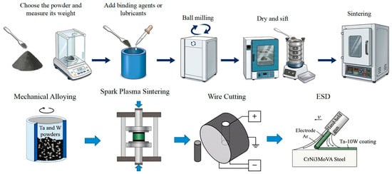
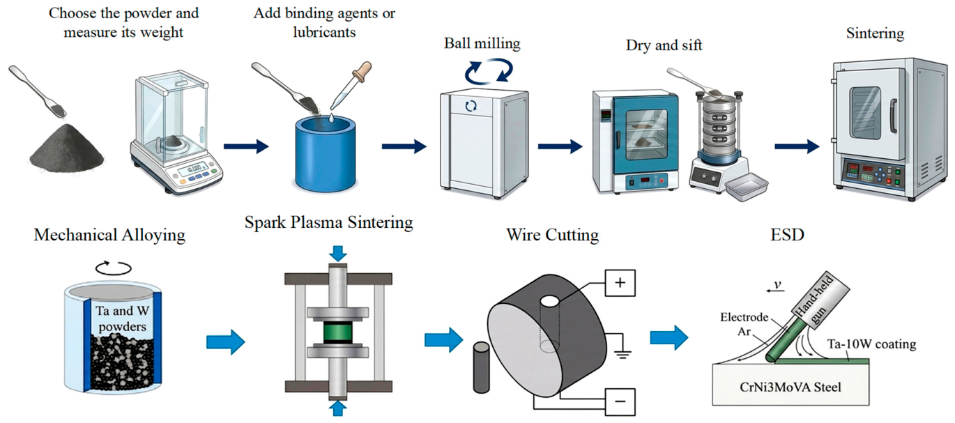
In this study, CrNi3MoVA steel was employed as the substrate material, with its precise chemical composition detailed in Table 1. Rectangular specimens with a length of 20 mm, a width of 10 mm, and a height of 5 mm were fabricated using wire electrical discharge machining (WEDM). The Ta-10W electrode (diameter: 4 mm; length: 50 mm) was fabricated via powder metallurgy. Specifically, tantalum powder (99.9% purity) and tungsten powder (99.5% purity) were combined at a mass ratio of 9:1 and subsequently sintered at 1500 °C under a pressure of 30 MPa for 2 h. Figure 1 depicts the overall preparation procedure. Both the substrate and the electrode surfaces were polished before deposition using 1000-grit abrasive paper and subjected to ultrasonic cleaning to eliminate any surface contaminants.
Table 1.
Chemical composition of CrNi3MoVA steel (wt.%).
Figure 1.
Preparation procedure of the Ta-10W electrode.
The nominal room-temperature mechanical properties of the CrNi3MoVA artillery-steel substrate used in this study: tensile strength ≥ 980 MPa, yield strength ≥ 885 MPa, elongation ≥ 10%, elastic modulus approximately 200–210 GPa, Poisson’s ratio 0.28–0.30 and hardness approximately 260–330 HB, depending on heat-treatment state. These values indicate that the substrate provides load support for the thin electricspark deposition coating, while its surface still requires protection against adhesive wear, thermo-chemical erosion and thermal softening under bore-service conditions [1].
2.2. Electricalspark Deposition Process
The deposition process was conducted in an argon atmosphere with oxygen concentration kept below 200 ppm, using the DJ-electricspark deposition 2000 apparatus (Shanghai Kangbei Mechanical and Electrical Equipment Co., Ltd., Jiading District, Shanghai, China). The voltage window was determined from preliminary deposition trials and from the known relationship between pulse voltage, stored discharge energy and heat input in electricspark deposition. At 60 V, a continuous coating could be obtained with limited splashing, representing the lower stable-deposition bound. At 100 V, the deposition process remained possible but exhibited obvious molten-droplet ejection and defect generation, representing the upper practical bound beyond which severe spalling and overheating were likely. Thus, 80 V was selected as an intermediate condition to evaluate the trade-off between material transfer and defect formation [18,19].
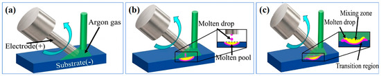
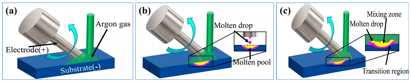
The process parameters were set as follows: deposition voltages of 60 V, 80 V, and 100 V, corresponding to deposition powers of 800 W, 1200 W, and 1500 W, respectively; an argon gas flow rate fixed at 1 L/min; an electrode rotation speed of 2500 rpm; and a deposition duration of 1 min/cm2. Figure 2 presents the schematic representation of the electricalspark deposition process.
Figure 2.
Schematic representation of the electricalspark deposition process: (a) before electrode contact; (b) embryo deposit; (c) settle for a period of time.
2.3. Material Characterization and Performance Evaluation
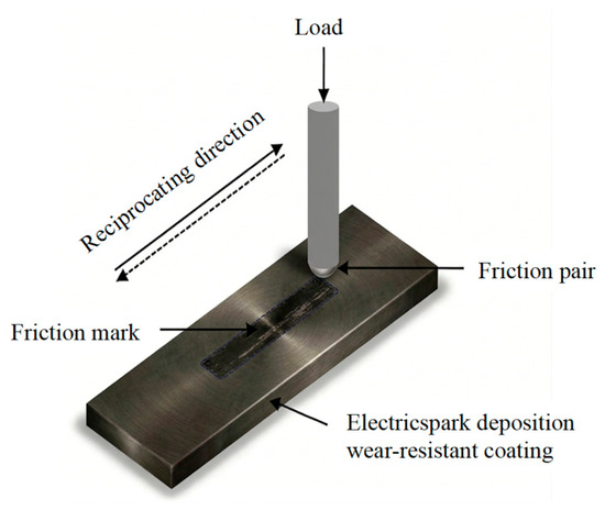
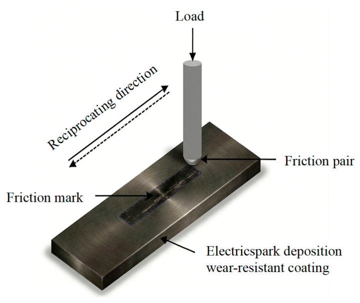
The surface and cross-sectional morphologies, along with the chemical compositions of the coatings, were examined using field emission scanning electron microscopy (FESEM, Gemini360, CarlZeissAG, Oberkochen, Germany). Phase identification before and after wear testing was conducted using X-ray diffraction (XRD, D8 Advance, Bruker, Karlsruhe, Germany) with Cu-Kα radiation. Surface hardness measurements were performed using a Vickers microhardness tester (FM-300, Future-Tech Corp., Kawasaki, Japan) under a load of 500 gf with a dwell time of 15 s. Ten indentations were performed for each sample to obtain the average microhardness value (HV0.5). The elastic modulus (E), nano-hardness (H), and the ratios H/E and H3/E2 of the coatings were determined using nanoindentation testing (Hysitron TI 950, Bruker, Germany). The tribological performance, which includes friction and wear behavior, was assessed using a reciprocating friction tester (HSR-2M, Lanzhou Zhongke Kaihua Technology Development Co., Lanzhou, China). Figure 3 displays the fundamental principle of the experiment. The friction pair consisted of a 304 stainless steel ball (diameter: 6 mm) subjected to a 6 N normal load, with a stroke length of 5 mm, an oscillation frequency of 2 Hz, and a total duration of 300 s. The wear loss was quantified using a precision electronic balance with an accuracy of 0.01 mg.
Figure 3.
Fundamental principle of friction and wear.
3. Results and Discussion
3.1. SEM Analysis of Coating Surface Morphology
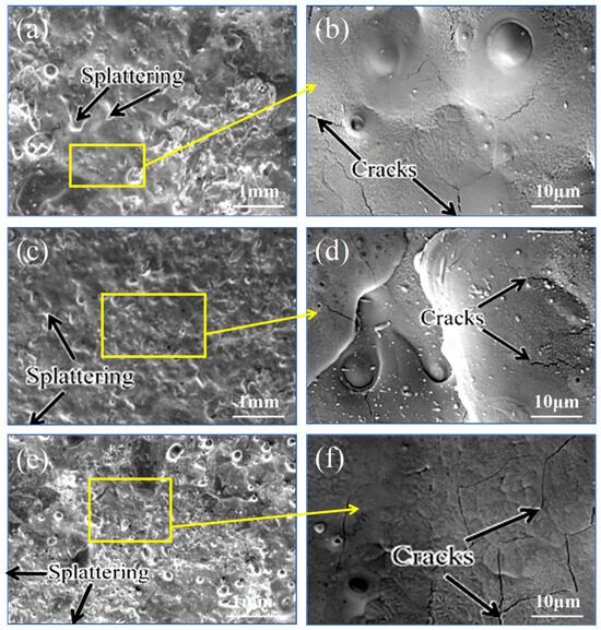
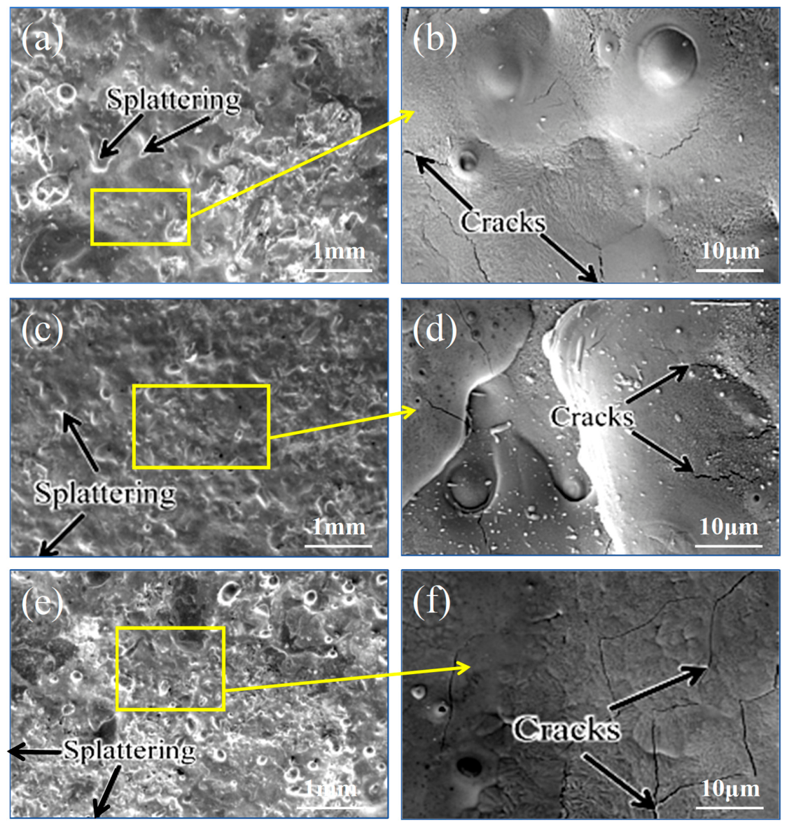
Figure 4 presents the SEM surface morphologies and corresponding area scan elemental distributions of Ta-10W coatings fabricated at deposition voltages of 60 V, 80 V, and 100 V. As shown in the figure, the surface characteristics and defect profiles of the coatings vary significantly with increasing voltage. Notably, all samples exhibit splatter marks on the coating surfaces, resulting from short-circuit events arising from direct contact between the electrode and substrate. These events trigger the instantaneous discharge of capacitor energy. The resultant current pulse generates a plasma arc with temperatures ranging from approximately 5000 K to 25,000 K over an extremely brief duration. This rapid thermal spike induces the formation of molten metal droplets at the electrode tip, which are subsequently ejected at high velocity onto the substrate surface. As the deposition voltage increases, the surface morphology transitions from a relatively smooth surface with minimal splattered particles at 60 V to the emergence of discernible pores and microcracks at 80 V.
Figure 4.
SEM surface morphologies of Ta-10W coatings deposited via electricspark deposition at (a,b) 60 V; (c,d) 80 V; and (e,f) 100 V.
Finally, a pronounced network of holes and cracks is formed at 100 V. This progression is primarily attributed to the correlation between higher voltage and increased discharge energy and heat input, intensifying droplet splashing and metal vaporization. The entrapment of gas within evaporation cavities contributes to elevated porosity, while steep temperature gradients and mismatches in thermal expansion during rapid solidification generate residual tensile stresses that facilitate crack initiation and propagation [20,21]. It should be noted that crack-free islands were also observed locally, especially at 60 V and 80 V; however, the high-magnification panels in Figure 4b,d,f were deliberately selected to display typical crack features so that voltage-dependent defect evolution could be compared. The coexistence of crack-free and cracked areas reflects the inherent spatial heterogeneity of electricspark deposition coatings. To obtain coatings with fewer defects, lower single-pulse energy, multi-pass deposition with reduced overlap heat accumulation, optimized argon shielding, moderate substrate preheating to decrease thermal gradients, and post-deposition surface remelting/polishing may be considered.
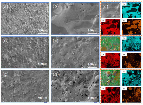
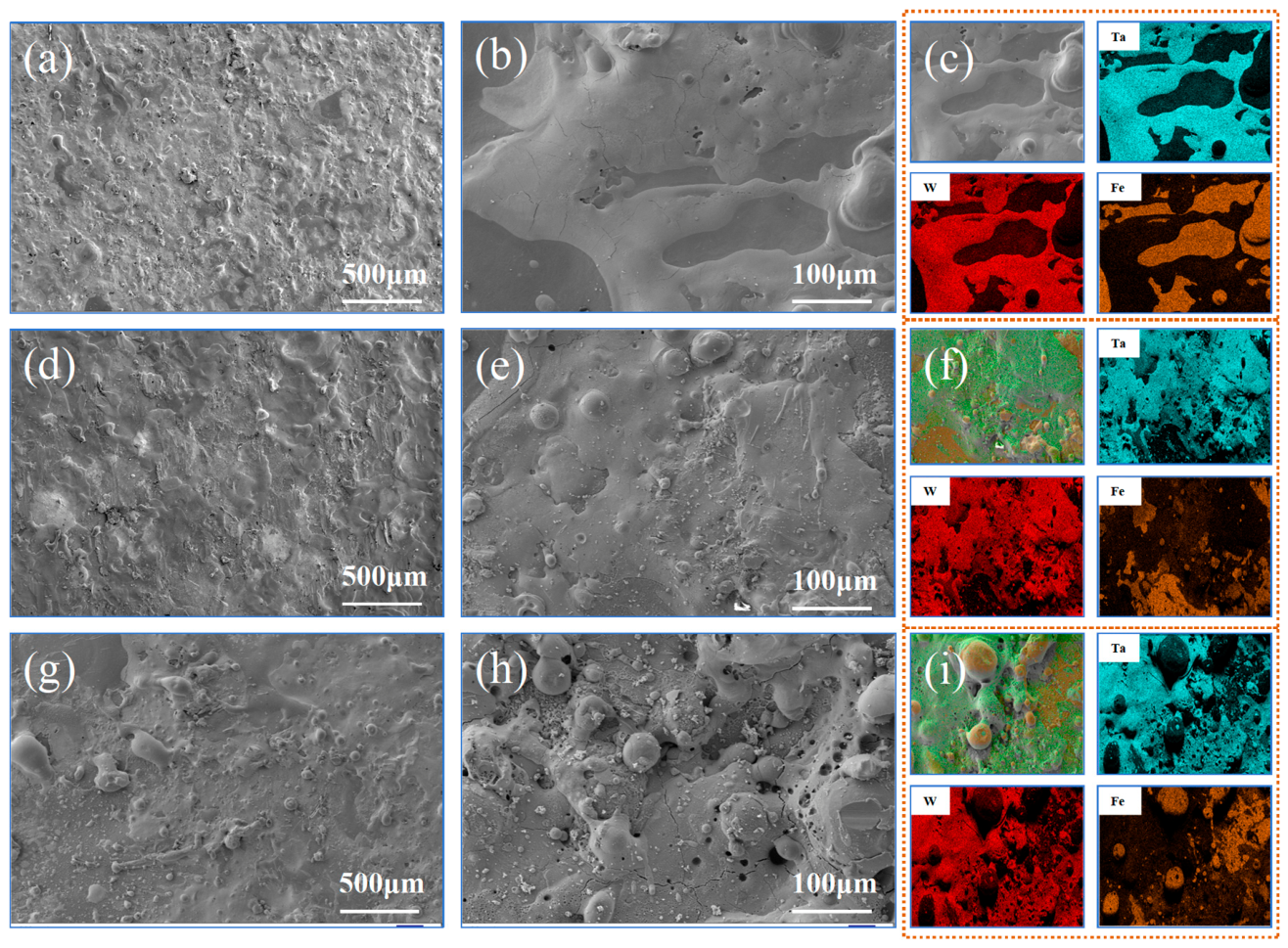
Figure 5 illustrates the surface morphology and the associated elemental distribution of Ta-10W coatings deposited under varying voltage conditions. Table 2 summarizes the quantitative elemental composition obtained from electricspark deposition, providing insight into the influence of voltage on material migration throughout the deposition process. The data indicate a general decrease in tantalum (Ta) content on the coating surface with increasing voltage, accompanied by increases in iron (Fe) and tungsten (W) concentrations. This pattern implies that higher voltages promote more intense localized melting and elemental intermixing, thereby amplifying substrate dilution effects. The molten pool depth and volume increase at higher voltages, enhancing the impact of discharge energy and facilitating greater mass transfer of substrate material into the coating. This process promotes local interactions between Fe and W or Ta, resulting in compositional gradients. Such elemental intermixing and gradients modify local mechanical properties, including elastic modulus, thermal expansion coefficients, and phase stability, thereby exacerbating interfacial stress concentrations and increasing susceptibility to crack formation [22,23].
Figure 5.
Surface morphology and the associated elemental distribution (c,f,i) of Ta-10W coatings deposited under varying voltage conditions: (a–c) 60 V; (d–f) 80 V; (g–i) 100 V.
Table 2.
Electricspark deposition quantitative results covering the whole surface (Figure 5) at different deposition voltage (At. %).
3.2. SEM Analysis of Coating Cross-Sectional Morphology
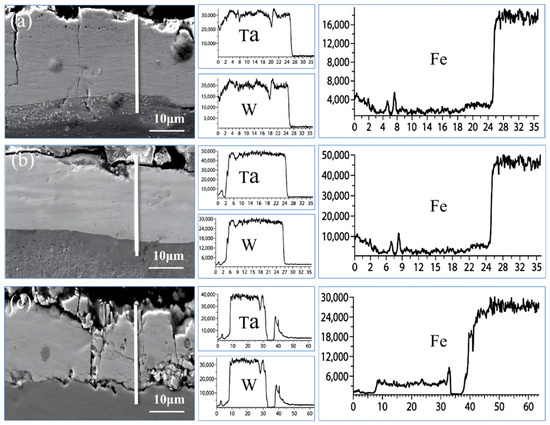
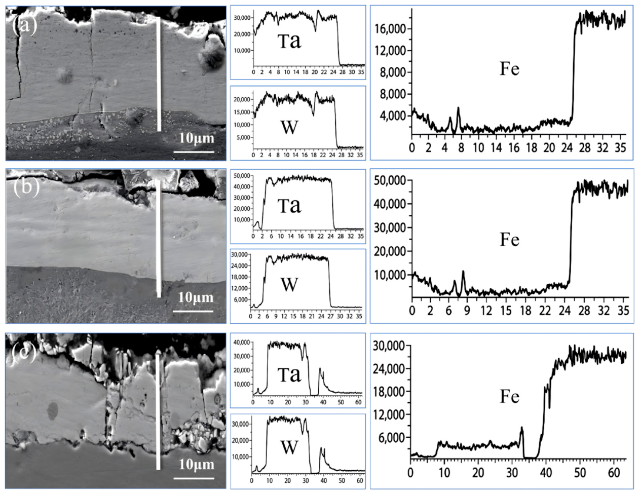
Figure 6 presents cross-sectional SEM micrographs of Ta-10W coatings deposited at different voltages, enabling comparative evaluation of coating thickness uniformity, porosity, crack distribution, and interfacial bonding quality. The cross-sections show a progressive defect evolution: isolated pores and short cracks are present at 60 V (Figure 6a), more internal pores and microcracks appear at 80 V (Figure 6b), and the most severe semi-penetrating cracks and local interfacial delamination occur at 100 V (Figure 6c). These phenomena are attributed to the substantial mismatch in thermal expansion coefficients between the Ta-10W coating, which has a relatively lower coefficient, and the steel substrate. The rapid thermal cycling induced by discharge pulses generates significant thermal strain mismatches. When pre-existing defects, such as pores or oxide inclusions, serve as crack initiation sites, the resulting thermal tensile stresses more readily drive crack propagation along structurally weak paths [24,25].
Figure 6.
Cross-sectional SEM images of Ta-10W coatings deposited by electricspark deposition at (a) 60 V, (b) 80 V, and (c) 100 V.
3.3. XRD Analysis of the Coatings
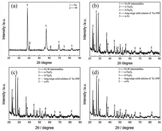
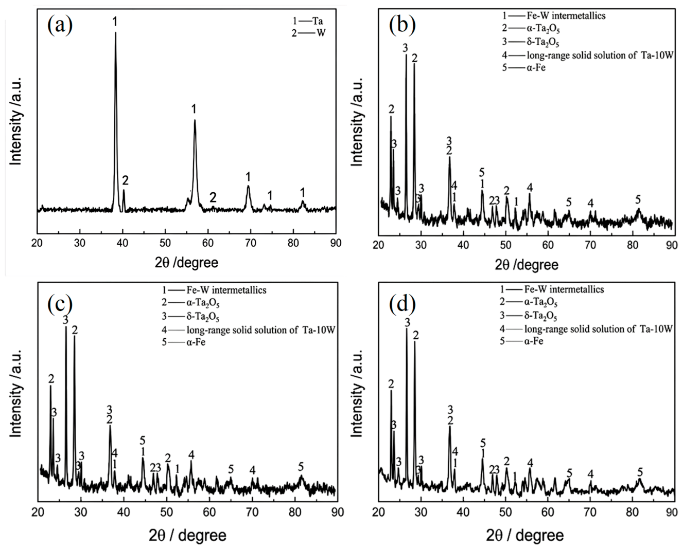
Figure 7 illustrates the XRD patterns of the Ta-10W electrode material alongside Ta-10W coatings deposited at varying voltages. These patterns were used to determine the principal phase composition of the coatings. As shown in Figure 7a–d, the coatings are primarily composed of α-Ta(W) solid solution diffraction peaks, accompanied by α-Ta2O5 and δ-Ta2O5 oxides, as well as α-Fe and Fe-W intermetallic compounds. The phase identification was carried out by matching the measured patterns with standard powder-diffraction reference data. The main reference cards considered were α-Ta (bcc, PDF# 04-0788), α-Fe (bcc, PDF# 06-0696), orthorhombic Ta2O5 (PDF# 25-0922), tetragonal α-Ta2O5 (PDF# 21-1199), hexagonal δ-Ta2O5 (PDF# 00-019-1299) and Fe-W intermetallic phase (PDF# 42-1209). Because the electricspark deposition coatings contain rapidly solidified and stressed phases with broad and partly overlapping peaks, the XRD data are used for qualitative phase identification in this work. Notably, the principal peak of the α-Ta(W) solid solution shifts relative to the standard Ta(110) diffraction peak shown in Figure 7a, indicating the incorporation of W atoms into the Ta lattice to form the α-Ta(W) solid solution.
Figure 7.
XRD patterns of electrode material of (a) and Ta-10W coatings at 60 V (b), 80 V (c), and 100 V (d).
The formation mechanism of this solid solution can be described as follows. First, the localized transient high temperatures generated by the electricspark deposition discharge facilitate the melting and intermixing of Ta and W. This is followed by an extremely rapid cooling process, which favors the retention of the solid solution by suppressing equilibrium phase separation. Second, trace amounts of oxygen may still be present despite the use of argon protection. Notably, Ta tends to oxidize under the combined influence of elevated temperature and high surface activity of the newly formed products, leading to the formation of oxide inclusions during droplet solidification. The EDS analysis in Table 2 supports the presence and redistribution of Ta, W, Fe and O elements, the phase assignments of α-Ta(W), α-Ta2O5, δ-Ta2O5 and α-Fe are based on XRD peak matching. This phase constitution explains the simultaneous presence of strengthening and embrittlement effects. The strengthening effect of α-Ta(W) is attributed to substitutional W atoms in the Ta lattice, which cause lattice distortion and impede dislocation motion, while hard oxide phases such as Ta2O5 contribute to dispersion/oxide strengthening. However, oxides and Fe-W intermetallic particles can also act as brittle inclusions and stress concentrators when they are located near pores or cracks. Therefore, this phase constitution can simultaneously increase hardness and reduce damage tolerance, which explains why a moderate voltage improves hardness whereas excessive voltage promotes crack-assisted degradation [14,26,27].
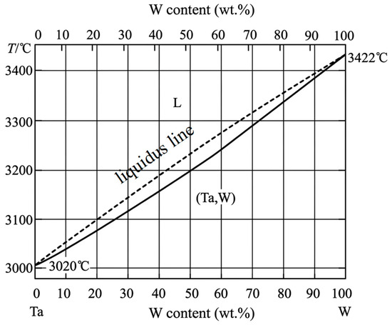
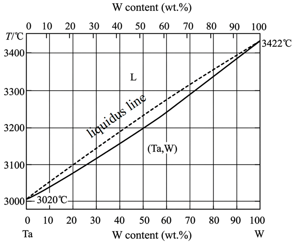
Figure 8 presents the Ta-W binary phase diagram [28]. During the electricspark deposition of Ta-10W alloy coatings, temperatures exceed 3000 °C, enabling the formation of Ta-10W solid solution microstructures under rapid solidification conditions. The thermal cycling inherent to electricspark deposition is characterized by a “high peak temperature, extremely short dwell time, and ultra-fast cooling rate,” representing a distinctly non-equilibrium process even though phase composition and solubility under equilibrium conditions depend on temperature. This facilitates uniform mixing of molten Ta and W and the subsequent formation of the Ta(W) solid solution upon solidification. The dissolution of W atoms into the Ta lattice induces lattice distortion and solid solution strengthening, increasing resistance to dislocation movement and enhancing the local load-bearing capacity. Consequently, this improves the coating’s ability to withstand plastic shear and plowing under frictional contact. The integration of these findings with the XRD analysis in Figure 7 shows that the Ta(W) solid solution is the primary strengthening phase responsible for the enhanced strength and wear resistance of the coating. This directly supports the observation that peak hardness is achieved at moderate voltages (e.g., 80 V).
Figure 8.
Ta-W binary phase diagram [28].
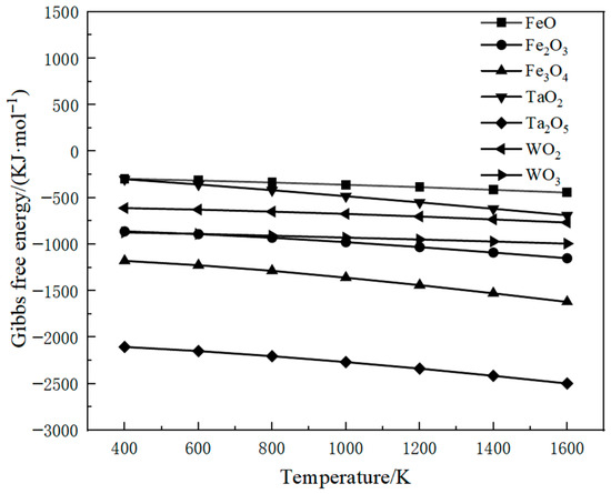
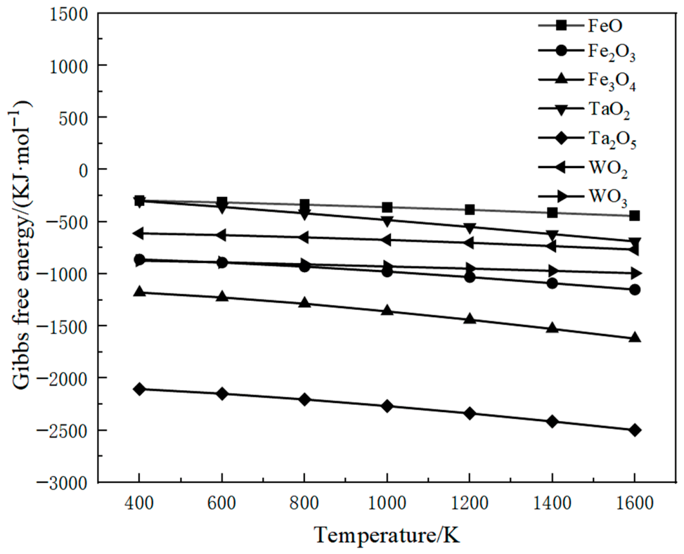
Figure 9 illustrates the variation in Gibbs free energy for oxides of Fe, Ta, and W at different temperatures [29]. As shown in Figure 9, Ta oxides exhibit the lowest Gibbs free energy. Therefore, oxide phases such as Ta2O5 are still detected during the preparation of Ta-10W coatings despite argon protection. Notably, oxidation is governed not only by the Gibbs free energy change (ΔG) but also by kinetic factors. According to electricspark deposition principles, the pulse energy and heat input increase with output voltage and capacitance. Therefore, higher voltages generally enhance electrode material transfer and coating growth but also increase molten-droplet spattering, metal vaporization, pore formation and thermal-stress cracking [18,19]. This mechanism supports the observed transition from relatively compact coatings at 60–80 V to a more defective morphology at 100 V. Table 3 summarizes the principal chemical reactions involving the elements during the coating preparation process. Thermodynamically, the Gibbs free energy (ΔG) values for Ta oxides are substantially lower than those for other oxides, indicating that their formation is a spontaneous reaction. This observation validates the presence of Ta oxide phases identified in Figure 7 and establishes a thermodynamic basis for their formation.
Figure 9.
Gibbs free energy changes in Ta, W, and Fe oxides at various temperatures [29].
Table 3.
Principal chemical reactions occurring in the Ta-10W coating during electricspark deposition.
3.4. Hardness Evaluation of the Coatings
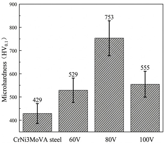
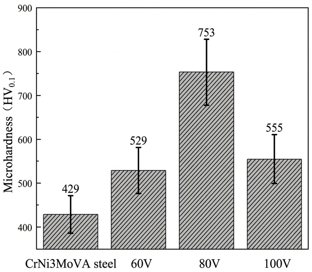
Figure 10 presents the microhardness measurements of Ta-10W coatings and the cannon steel substrate subjected to varying deposition voltages. This enables evaluation of the influence of voltage on the coatings’ macroscopic load-bearing capacity. The data reveal substantially higher hardness in the coatings than in the substrate. The hardness varies non-linearly with voltage, increasing from approximately 530 HV at 60 V to a peak of around 753 HV at 80 V, followed by a decline to roughly 556 HV at 100 V. Based on the integration of these findings with the SEM analyses of surface and cross-sectional morphologies depicted in Figure 4 and Figure 6, it is inferred that the hardness enhancement from 60 V to 80 V primarily results from work hardening induced by Ta(W) solid solution strengthening and the formation of hard oxide phases. These mechanisms collectively improve resistance to plastic deformation under contact loading. Conversely, Figure 6c confirms that the 100 V coating contains the highest density of pores, microcracks and semi-penetrating cracks. These structural discontinuities interrupt the effective load-bearing path during Vickers indentation and reduce the apparent hardness, even though the higher voltage promotes melting, dilution and oxide/solid-solution formation. These observations suggest that a deposition voltage of 80 V optimally balances the “strengthening effect” and “structural integrity,” providing critical guidance for process parameter optimization.
Figure 10.
Surface microhardness of Ta-10W coatings and CrNi3MoVA steel.
During nanoindentation, the indents were selected from compact regions away from obvious pores and cracks as far as possible. Table 4 summarizes the elastic modulus (E) and nano-hardness (H) obtained from nanoindentation, along with the derived H/E and H3/E2 ratios for the various coatings. The H/E ratio is commonly used as an elastic strain or ductility index, while H3/E2 has been widely used as a plastic deformation resistance index. These parameters serve as indicators of the coatings’ potential wear resistance, as they reflect their elastic strain tolerance and resistance to plastic deformation. Overall, the coatings exhibit higher H/E and H3/E2 values compared to the substrate, indicating an enhanced ability to accommodate elastic strain and greater resistance to plastic shear or yielding during frictional wear, which is typically associated with improved wear performance, although they should not be treated as universal substitutes for direct fracture-toughness measurements [30,31,32]. The 60 V and 80 V coatings show comparable H/E values (0.025 and 0.024), indicating similar elastic accommodation capacity. The H3/E2 value of the 80 V coating (0.0024) is slightly lower than that of the 60 V coating (0.0025) but remains higher than that of the 100 V coating (0.0020); therefore, the superior engineering performance of the 80 V coating should be understood as a balance among high hardness, acceptable elastic/plastic indices and lower defect severity. Meanwhile, the performance deteriorates at 100 V due to structural defects.
Table 4.
Nano-mechanical properties of Ta-10W coatings and CrNi3MoVA steel.
3.5. Tribological Performance and Wear Mechanisms of the Coatings
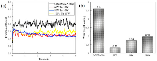
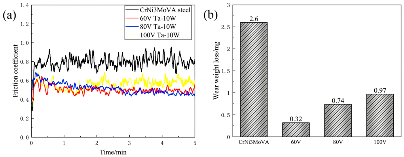
Figure 11 illustrates the friction and wear test results for the Ta-10W coatings and CrNi3MoVA steel substrate. Figure 11a depicts the friction coefficient as a function of time under a 6 N reciprocating load for the different samples. Figure 11b presents a comparison of the wear volumes of the coatings and the substrate across varying deposition voltages, elucidating the overall impact of voltage on tribological behavior. The substrate exhibits the highest friction coefficient, which ranges from 0.7 to 0.81, whereas the Ta-10W coatings significantly reduce friction. While friction coefficients remain comparable at 60 V and 80 V (0.55–0.58), the coefficient at 100 V increases significantly to approximately 0.63. As demonstrated in Figure 11b, the Ta-10W coatings enhance the wear resistance of CrNi3MoVA steel. Analyses indicate that the coatings deposited at 60–80 V exhibit more stable load-bearing continuity and minimal spallation. Consequently, friction processes favor the formation of relatively stable transfer films, leading to consistent friction levels with minimal fluctuations. In contrast, the coating deposited at 100 V, which is characterized by increased crack density and porosity, is more prone to debris generation and flake spallation under reciprocating loads, resulting in elevated friction coefficients. Overall, these results confirm that all coatings significantly improve wear resistance. Considering hardness enhancement, frictional behavior, and crack resistance, the 80 V deposition voltage is the optimal parameter for overall engineering performance.
Figure 11.
Friction and wear test results of Ta-10W coatings and CrNi3MoVA steel: (a) coefficient of friction; (b) wear volume.
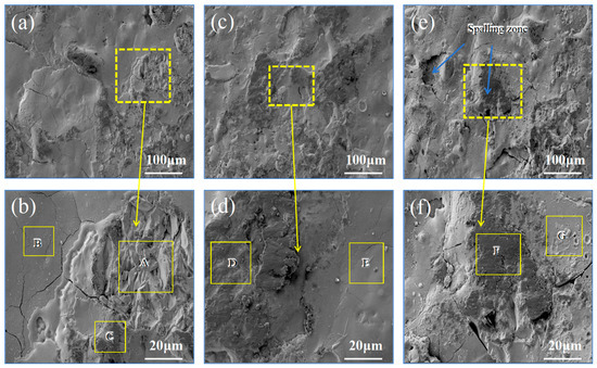
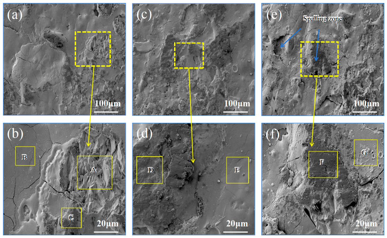
Figure 12 presents SEM micrographs of wear scars on coatings deposited at different voltages, highlighting wear morphology and dominant wear mechanisms. Figure 12a illustrates that the wear surface of the 60 V coating exhibits sparse adhesive wear spots, indicating adhesive wear as the primary mechanism at this voltage. The wear scars of the 80 V coating show pronounced adhesive regions alongside localized plastic deformation features (Figure 12c), while the 100 V coating reveals extensive spallation pits and flake-like delamination zones, signifying a transition from adhesive wear to crack-assisted spallation. When considered alongside the surface morphology data in Figure 4, higher voltages are associated with heightened coating defects (porosity, microcracks, compositional gradients) and elevated residual tensile stresses. These promote stress concentration at crack tips under reciprocating shear loads, facilitating crack propagation and flake spallation. The resultant spallation debris and oxide wear particles collectively generate a rough and unstable tribological interface, exacerbating friction and wear [33,34].
Figure 12.
SEM wear morphology of Ta-10W coatings: 60 V (a,b); 80 V (c,d); 100 V (e,f).
To monitor material transfer, oxidation, and substrate exposure during wear, EDS analyses were conducted on rectangular regions of the wear scars depicted in Figure 12b,d,f. The corresponding EDS data are presented in Table 5. Comparative analysis reveals significant enrichment of Fe and O in all wear scar regions, indicating that oxidized debris and transfer films originating from the stainless steel counterface contribute to friction interface formation. Furthermore, the coatings deposited at higher voltages show elevated Fe content, suggesting increased substrate exposure or participation in wear processes following localized coating spallation. The frictional heat generated during reciprocating wear accelerates oxidation of wear debris, and the resulting oxide particles, combined with coating spallation fragments, form complex multi-component tribological products. When these products are stable, they suppress wear by mitigating direct metal-to-metal contact. At 100 V, however, frequent crack-induced spallation causes rapid renewal and coarsening of these products, promoting severe plowing wear morphology, increased friction coefficients, and aggravated wear [35,36].
Table 5.
EDS results of wear at different positions of the Ta-10W coating.
Table 5 presents the EDS results for wear at various locations on the Ta-10W coating. A detailed examination of these data elucidates the relationship between the wear mechanisms and the hardness of the coating. The coating deposited at 60 V demonstrates relatively low hardness (530 HV) with a high hardness-to-elastic modulus ratio (H/E = 0.025), suggesting a comparatively elevated elastic limit. The contact stress remains beneath the yield strength of the coating under frictional conditions, resulting in wear predominantly governed by adhesive mechanisms (Figure 12a). At this stage, minor material transfer occurs between a 304 stainless steel ball counterface and the coating surface, forming localized adhesive regions; EDS analysis reveals an iron (Fe) content of 42.19% in area A. In contrast, the 80 V coating exhibits an increased hardness of 753 HV. However, the H/E ratio slightly decreases to 0.024, suggesting a diminished elastic limit. The elevated hardness concentrates frictional contact stresses in localized zones, inducing severe adhesive wear accompanied by plastic deformation (Figure 12c). The corresponding data indicate an Fe content of 62.53% in area D, suggesting substrate exposure due to localized spalling of the coating. The 100 V coating is characterized by the presence of delamination cracks that create structural discontinuities; the crack tips act as stress concentration sites under cyclic loading, culminating in fatigue-induced spalling (Figure 12e). The extensive spalled regions on the worn surface, with an Fe content of 71.55% in area F, indicate inadequate bonding strength between the coating and substrate, consistent with the coating’s lowest H3/E2 value of 0.002.
3.6. Crack Formation Mechanism and Finite Element Stress Analysis
The electricspark deposition process entails rapid melting followed by rapid solidification. During this process, energy is absorbed by both the electrode material and a portion of the substrate. This energy is converted into heat that melts these materials to form a molten pool. Most of the thermal energy is concentrated within the molten pool and the adjacent substrate, generating a pronounced temperature gradient that induces thermal stresses in both the coating and the substrate near the molten pool. These thermal stresses arise from two main sources: mismatch in material properties, such as elastic modulus and thermal expansion coefficient, between the Ta-10W alloy and the steel substrate, and heterogeneous solidification shrinkage within the molten pool itself.
Table 6 details the material properties of CrNi3MoVA steel and the Ta-10W coating. These data are effective parameters used for the thermo-mechanical simulation. The density, specific heat, thermal conductivity and thermal expansion coefficients were taken from literature/material-handbook values for CrNi3MoVA steel and Ta-10W alloy, whereas the coating elastic modulus was cross-checked with the nanoindentation results in Table 4. Thus, the values should be regarded as effective model inputs rather than direct bulk measurements for every local phase within the coating.
Table 6.
Material properties of the CrNi3MoVA steel and Ta-10W coating.
During electricspark deposition, the instantaneous contact between the electrode and substrate generates a high-energy plasma arc in the temperature range of 5000–25,000 K, thereby producing a substantial temperature gradient at the coating-substrate interface. The disparity in thermal expansion coefficients 6 × 10⁻⁶ K−1 for the Ta-10W coating and 12 × 10−6 K−1 for the CrNi3MoVA steel substrate-causes the coating to contract less than the substrate upon cooling. This differential contraction induces tensile stress (σT) at the interface. The quantification of this stress can be derived using the thermoelastic mechanics Equation (1) as follows:
In Equation (1), σT denotes the thermal stress, αcoating and αsubstrate correspond to the thermal expansion coefficients of the electrode and substrate materials, respectively; ΔT represents the temperature differential between the coating solidification temperature (approximately 800 °C) and ambient room temperature (25 °C); E and ν signify the Young’s modulus and Poisson’s ratio of the electrode material, respectively.
The thermal stress σT for the 100 V coating is estimated to be approximately 1150 MPa by inputting the material parameters (E = 220 GPa, ν = 0.32) into the equation. This substantially surpasses the yield strength of the Ta-10W coating (555 MPa). This tensile stress initiates microcracks within the coating, which subsequently propagate along grain boundaries or pre-existing defects under cyclic thermal shocks caused by repeated deposition pulses.
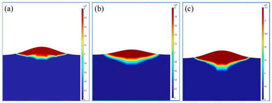
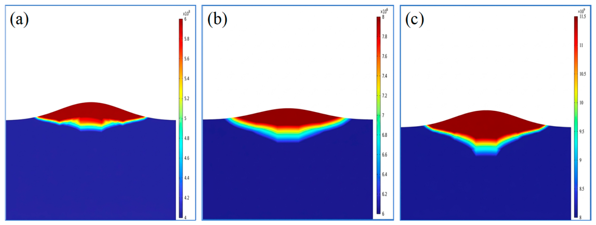
Figure 13 presents finite element simulation contour maps depicting the distribution of the deposition stress field in Ta-10W coatings fabricated at varying deposition voltages, which quantitatively validate crack evolution. As the voltage increases from 60 V to 80 V, the maximum equivalent stress within the coating cross-section escalates sharply from 600 MPa to 800 MPa. Despite approaching the coating’s yield strength, the maximum stress does not induce delamination cracks. However, as the voltage increases further from 80 V to 100 V, the maximum equivalent stress at the coating-substrate interface rises from 800 MPa to 1150 MPa. This value significantly exceeds the yield strength of the Ta-10W coating, leading to fracture and crack formation proximal to the interface. This behavior is consistent with the experimentally observed increase in crack density as voltage increases.
Figure 13.
Cloud map depicting the distribution of the deposition stress field within the Ta-10W coatings at varying deposition voltages of (a) 60 V, (b) 80 V, and (c) 100 V.
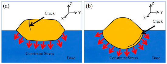
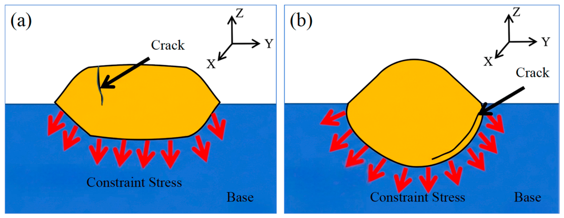
Fundamentally, higher deposition voltages correspond to elevated heat fluxes and steeper temperature gradients, intensifying thermal strain mismatches and generating stress concentration zones near the interface. When the equivalent stress surpasses the coating’s effective strength or fracture toughness threshold, cracks initiate at pores or oxide inclusions and propagate toward the interface, promoting delamination and spalling wear. The simulation results underscore the substantial influence of deposition voltage on the integrity of Ta-10W coatings produced via electricspark deposition. The thermal stress in the 100 V coating exceeds the yield limit when combined with thermoelastic mechanics calculations (Equation (1)), facilitating crack propagation along the deposited layer (as depicted in Figure 14). This phenomenon aligns with Griffith’s fracture mechanics theory, which defines the critical condition for crack propagation as follows:
Figure 14.
Formation and propagation mechanisms of cracks: (a) longitudinal cracks and (b) transverse cracks.
In Equation (2), γ denotes the surface energy, while a corresponds to the half-length of the crack. The combined influence of thermal stress (σ) and the size of coating defects (a) synergistically accelerates the failure of the coating at elevated voltage conditions.
4. Conclusions
In conclusion, this study successfully fabricated Ta-10W coatings on CrNi3MoVA steel substrates via the electricspark deposition technique. Furthermore, a systematic analysis was conducted to elucidate the effect of deposition voltage on coating performance, yielding the following principal conclusions:
- (1)
- According to SEM and XRD analyses, the coating microstructure consists of α-Fe, α-Ta2O5, δ-Ta2O5, α-Ta(W), and Fe-W intermetallic phases. An increase in deposition voltage from 60 V to 100 V enhanced the coating thickness; however, this was accompanied by a higher incidence of pores and cracks. Notably, the coating deposited at 100 V exhibited through-thickness delamination cracks due to accumulated thermal stress reaching 1150 MPa, substantially undermining its structural integrity.
- (2)
- Microhardness and nanohardness measurements indicated that the coating deposited at 80 V attained the highest hardness value of 753 HV. Its H3/E2 ratio of 0.0024 signifies superior resistance to plastic deformation. In contrast, the hardness of the 100 V coating decreased significantly to 556 HV, a decline attributed to crack propagation.
- (3)
- The coating deposited at 60 V predominantly underwent adhesive wear, exhibiting the lowest wear loss of 0.5 mg. In contrast, the 100 V coating experienced spalling wear caused by structural defects, resulting in an increased wear loss of 0.63 mg.
- (4)
- Process optimization identified 80 V as the optimal deposition voltage, effectively balancing enhanced hardness with a manageable defect density.
Author Contributions
Conceptualization, C.G. and G.Z.; methodology, G.Z.; software, G.Z., W.S.; J.S. and J.Y.; validation, C.G., G.Z., W.S. and L.H.; formal analysis, G.Z. and W.S.; investigation, C.G.; resources, C.G.; data curation, J.Y., J.S., W.S. and G.Z.; writing—original draft preparation, G.Z.; writing—review and editing, C.G.; visualization, L.H.; supervision, C.G.; project administration, C.G.; funding acquisition, G.Z. All authors have read and agreed to the published version of the manuscript.
Funding
The study is supported by the Research Project of the Education Department of Liaoning Province of China (1030040000675), Research support funding for attracting high-level talents in 2025 (6030109777), 2026 Liaoning Province Doctoral Research Launch Project, Shenyang Municipal Special Project for Scientific and Technological Talents (RC23095), Special Fund of Basic Scientific Research Operating Expense of Undergraduate Universities in Liaoning Province (LJ212410144077), Financial support of the Key R&D Project of the Joint Science and Technology Program of Liaoning Province (2025JH2/101800434).
Data Availability Statement
The original contributions presented in this study are included in the article. Further inquiries can be directed to the corresponding author.
Conflicts of Interest
Jinpeng Yang was employed by the company Norinco Group, Aviation Ammunition Institute, Harbin 150030, China. The remaining authors declare that the research was conducted in the absence of any commercial or financial relationships that could be construed as a potential conflict of interest.
References
- Sopok, S.; Rickard, C.; Dunn, S. Thermal-chemical-mechanical gun bore erosion of an advanced artillery system part one: Theories and mechanisms. Wear 2005, 258, 659–670. [Google Scholar] [CrossRef] [Scilit]
- Niu, Y.; Zhang, M.; Wang, Q.; Zhang, C.; Liu, N.; Huang, J.; Chen, M.; Zhu, S.; Wang, F. Failure mechanism of sputtered Ta coatings on short rifled gun bore under vented vessel tests. npj Mater. Degrad. 2025, 9, 36. [Google Scholar] [CrossRef] [Scilit]
- Barile, C.; Casavola, C.; Pappalettera, G.; Renna, G. Advancements in Electrospark Deposition (ESD) Technique: A Short Review. Coatings 2022, 12, 1536. [Google Scholar] [CrossRef] [Scilit]
- Mani, G.; Porter, D.; Grove, K.; Collins, S.; Ornberg, A.; Shulfer, R. A comprehensive review of biological and materials properties of Tantalum and its alloys. J. Biomed. Mater. Res. Part A 2022, 110, 1291–1306. [Google Scholar] [CrossRef] [Scilit]
- Sopata, M.; Karpiński, T.M.; Jakubowicz, J.; Sopata, M. Development of tantalum with highly hydrophilic surface and antimicrobial properties obtained by micro-arc oxidation process. J. Biomed. Mater. Res. Part B Appl. Biomater. 2021, 109, 829–840. [Google Scholar] [CrossRef] [Scilit]
- Sopata, M.; Siwak, P.; Adamek, G.; Jakubowicz, J. The mechanical properties of the novel nanocrystalline refractory tantalum alloys. Prot. Met. Phys. Chem. Surf. 2020, 56, 759–765. [Google Scholar] [CrossRef] [Scilit]
- Li, S.X.; Xu, Y.; Xia, H.Q.; Duan, J.; Yu, Y.J.; Duan, X.Y.; Shi, P.F.; Tang, J.C. Tribological behaviors of tantalum prepared by SPS under different loads. Ind. Lubr. Tribol. 2023, 75, 959–965. [Google Scholar] [CrossRef] [Scilit]
- Jakubowicz, J.; Adamek, G.; Sopata, M.; Koper, J.K.; Kachlicki, T.; Jarzebski, M. Microstructure and electrochemical properties of refractory nanocrystalline Tantalum-based alloys. Int. J. Electrochem. Sci. 2018, 13, 1956–1975. [Google Scholar] [CrossRef] [Scilit]
- Yu, Y.; Xu, Y.; Duan, X.; Zhu, S.; Lei, Y.; Xia, H.; Wang, A.; Jiang, Q.; Tang, J. Process optimization and performance of spark plasma sintered Ta-10W alloy. Intermetallics 2024, 175, 108495. [Google Scholar] [CrossRef] [Scilit]
- Zuo, J.D.; Wang, Y.Q.; Wu, K.; Zhang, J.Y.; Liu, G.; Sun, J. Composition-mediated abnormal phase evolution in Ta-W films with Cr buffer layers. Scr. Mater. 2024, 238, 115759. [Google Scholar] [CrossRef] [Scilit]
- Wang, S.; Wu, Z.H.; Xie, M.Y.; Si, D.H.; Li, L.Y.; Chen, C.; Zhang, Z.; Wu, Y.C. The effect of tungsten content on the rolling texture and microstructure of Ta-W alloys. Mater. Charact. 2020, 159, 110067. [Google Scholar] [CrossRef] [Scilit]
- Liu, T.X.; Guo, C.A.; Lu, F.S.; Zhang, X.Y.; Zhang, L.; Wang, Z.J.; Xu, Z.Y.; Zhu, G.L. Influence of deposition voltage on tribological properties of W-WS2 coatings deposited by electrospark deposition. Chalcogenide Lett. 2023, 20, 741–749. [Google Scholar] [CrossRef] [Scilit]
- Bogdanoff, D.W. Use of a Tantalum Liner to Reduce Bore Erosion and Increase Muzzle Velocity in Two-Stage Light Gas Guns. In Proceedings of the 66th Meeting of the Aeroballistic Range Association, San Antonio, TX, USA, 4–9 October 2015. [Google Scholar]
- Wang, Z.; Zhu, G.; Lv, K.; Li, J.; Yu, X.; Yu, Y.; Guo, C.; Zhang, J. Research Progress on Preparation, Microstructure, Properties, and Optimization of Ta and Its Compounds’ Coatings. Metals 2025, 15, 416. [Google Scholar] [CrossRef] [Scilit]
- Yang, H.L.; Chen, X.M.; Chen, L.; Wang, Z.; Hou, G.; Guo, C.; Zhang, J. Influence of temperature on tribological behavior of AlCoCrFeNi coatings prepared by electrospark deposition. Dig. J. Nanomater. Biostruct. 2023, 18, 145–156. [Google Scholar] [CrossRef] [Scilit]
- Wang, Z.; Zhu, G.; Lu, F.; Zhang, L.; Wang, Y.; Zhao, S.; Guo, C.; Zhang, J. Friction and wear performance of an electrospark-peposited Ta coating on CrNi3MoVAST. Mater. Technol. 2024, 58, 17–23. [Google Scholar]
- Wu, J.; Shen, M.; Hu, M.; Guo, C.; Li, Q.; Zhu, S. High vacuum arc ion plating Cr films: Self-ion bombarding effect and oxidation behavior. Corros. Sci. 2021, 187, 109476. [Google Scholar] [CrossRef] [Scilit]
- Johnson, R.N. Electrospark Deposition: Principles and Applications. In Proceedings of the 45th Annual Technical Conference; Society of Vacuum Coaters: Albuquerque, NM, USA, 2002; pp. 87–92. [Google Scholar]
- Zhang, J.B.; Zhu, C. Research and application progress of electrospark deposition technology. Mater. Rep. 2023, 37, 22030015-14. (In Chinese) [Google Scholar]
- Yin, P.; Xu, C.; Pan, Q.; Zhang, W.; Jiang, X. Effect of Different Ultrasonic Power on the Properties of RHA Steel Welded Joints. Materials 2022, 15, 768. [Google Scholar] [CrossRef] [Scilit]
- Yang, P.; Lu, N.; Liang, J.; Guo, Y.; Zhang, G.; Song, X.; Zhou, Y.; Sun, X.; Li, J. Hot Crack Formation Mechanism and Inhibition of a Novel Cobalt-Based Alloy Coating during Laser Cladding. Materials 2024, 17, 3914. [Google Scholar] [CrossRef] [Scilit]
- Yamanaka, K.; Mori, M.; Sato, K.; Chiba, A. Characterisation of nanoscale carbide precipitation in as-cast Co–Cr–W-based dental alloys. J. Mater. Chem. B 2016, 4, 1778–1786. [Google Scholar] [CrossRef] [Scilit]
- Wang, Y.J.; Lyu, Z.; Wu, Z.S.; Li, L.J. Effect of Fusion Boundary Microstructure on Flow-Accelerated Corrosion Cracking. Materials 2024, 17, 2026. [Google Scholar] [CrossRef] [Scilit]
- Rau, A.V.; Lu, K. Twice-Functionalized Montmorillonite Nanosheets for Polymer-Derived MMT-SiOC Nanocomposites: Phase Formation and Porosity. Small 2025, 21, e2408218. [Google Scholar] [CrossRef] [Scilit] [PubMed]
- Zhang, S.; Bi, Z.; Li, J. Investigating the effect of microstructure difference on hydrogen embrittlement sensitivity of X80 pipeline. Sci. Rep. 2025, 15, 37057. [Google Scholar] [CrossRef] [Scilit] [PubMed]
- Pavlina, E.J.; Van Tyne, C.J. Correlation of yield strength and tensile strength with hardness for steels. J. Mater. Eng. Perform. 2008, 17, 888–893. [Google Scholar] [CrossRef] [Scilit]
- Tsui, T.Y.; Pharr, G.M.; Oliver, W.C.; Bhatia, C.S.; White, R.L.; Anders, S.; Anders, A.; Brown, I.G. Nanoindentation and nanoscratching of hard carbon coatings for magnetic disks. MRS Online Proc. Libr. 1995, 383, 447–452. [Google Scholar] [CrossRef] [Scilit]
- Moffatt, W. The Handbook of Binary Phase Diagrams; General Electric Company Research and Development: Schenectady, NY, USA, 1984. [Google Scholar]
- Liang, Y.J.; Che, Y.C. Thermodynamic Data Handbook of Inorganic Substances; Northeastern University Press: Shenyang, China, 1993. (In Chinese) [Google Scholar]
- Leyland, A.; Matthews, A. On the significance of the H/E ratio in wear control: A nanocomposite coating approach to optimised tribological behaviour. Wear 2000, 246, 1–11. [Google Scholar] [CrossRef] [Scilit]
- Chen, X.; Du, Y.; Chung, Y.-W. Commentary on using H/E and H3/E2 as proxies for fracture toughness of hard coatings. Thin Solid Film. 2019, 688, 137265. [Google Scholar] [CrossRef] [Scilit]
- Lozynskyi, V.; Trembach, B.; Hossain, M.M.; Kabir, M.H.; Silchenko, Y.; Krbata, M.; Sadovyi, K.; Kolomiitse, O.; Ropyak, L. Prediction of phase composition and mechanical properties Fe-Cr-C-B-Ti-Cu hardfacing alloys: Modeling and experimental validations. Heliyon 2024, 10, e25199. [Google Scholar] [CrossRef] [Scilit]
- Liu, R.; Cao, L.; Liu, D.D.; Wang, L.; Saeed, S.; Wang, Z.B. Laser Interference Lithography—A Method for the Fabrication of Controlled Periodic Structures. Nanomaterials 2023, 13, 1818. [Google Scholar] [CrossRef] [Scilit]
- Kiefel, A.; Gimmler, S.; Broeckmann, C.; Vroomen, U. Zn-Based Alloys for Plain Bearings—Influence of Al and Cu Content on Mechanical Properties. Materials 2024, 17, 1062. [Google Scholar] [CrossRef] [Scilit]
- Kim, J.H.; Kim, W.S.; Yoo, Y. Friction Properties of Solid Lubricants with Different Multiwalled Carbon Nanotube Contents. Materials 2022, 15, 4054. [Google Scholar] [CrossRef] [Scilit]
- Anioek, K.; Barylski, A.; Kupka, M.; Leszek, I. The Tensile Properties, Scratch Behaviors and Sliding Wear of Oxide Scale Formed on Titanium Grade 2. Materials 2020, 13, 3048. [Google Scholar] [CrossRef] [Scilit]

Disclaimer/Publisher’s Note: The statements, opinions and data contained in all publications are solely those of the individual author(s) and contributor(s) and not of MDPI and/or the editor(s). MDPI and/or the editor(s) disclaim responsibility for any injury to people or property resulting from any ideas, methods, instructions or products referred to in the content. |
© 2026 by the authors. Licensee MDPI, Basel, Switzerland. This article is an open access article distributed under the terms and conditions of the Creative Commons Attribution (CC BY) license.