


Abstract
Lead-free perovskite solar cells are promising as sustainable photovoltaics, but most of the copper-based alternatives are inefficient and unstable. The copper(I) perovskite chlorides (CuMCl3, M = Fe, Cr, Zn) are optimized by tuning the thickness and doping of the TiO2 electron transport layer, CuMCl3 absorber, and Spiro-OMeTAD hole transport layer, respectively, using SCAPS-1D simulations. The notable performance of CuZnCl3 (Voc = 0.79 V, Jsc = 38.2 mA·cm−2, FF = 80.2%) is observed due to the comparatively small bandgap (~1.10 eV) and appropriate thickness of the absorber (700 nm), achieving a balance between the generation of photocurrent and bulk recombination. The optimized n-i-p configuration yields power conversion efficiencies of 9.7% (CuFeCl3), 21.4% (CuCrCl3), and a relatively high 24.2% (CuZnCl3). CuCrCl3 works effectively (Voc = 0.99 V, Jsc = 25.1 mA·cm−2, FF = 86.15%) because it has a high dielectric constant and enables long diffusion. CuZnCl3 has a relatively good initial efficiency but considerable thermal sensitivity at 300–345 K, whereas CuFeCl3 has negligible thermal sensitivity. A rise in trap density leads to cation-dependent performance loss in all devices. This study proposes CuMCl3 as a promising lead-free perovskite platform for future photovoltaics.
1. Introduction
In recent years, perovskite solar cells have emerged as the most efficient photovoltaic technology. They can convert light into electricity with an efficiency of more than 26%, whereas silicon took decades to achieve [1,2]. The outstanding photonic properties of ABX3-structured perovskite materials, such as long charge-carrier diffusion lengths, high absorption coefficients, tunable energy bandgap, and the ability to tolerate substantial defects, contribute to these significant achievements [3,4]. However, the most effective perovskites rely on lead (Pb) metal, a hazardous material with serious health and environmental consequences. While lead-based perovskite solar cells are a promising technology, their toxicity and long-term stability present significant barriers to public and commercial acceptance. As a result, a significant global research initiative has focused on non-toxic alternatives to perovskite solar cells [5].
Despite this, lead-free perovskites have had problems closing the efficiency gap so far, showing unstable oxidation states, indirect bandgaps, or poor carrier transport. This is a significant opportunity to quickly find completely new types of lead-free absorbers that can work as well as their lead-based counterparts while also being naturally stable [6,7]. We are interested in copper(I) perovskite chlorides (CuMCl3, where M = Fe, Cr, Zn), a group of compounds that has not been studied enough. These perovskites possess direct, tunable bandgaps (1.10–2.02 eV) that approach the Shockley–Queisser threshold for peak photovoltaic efficiency, reduced formation energies, and enhanced carrier mobilities due to their lowered effective masses [8,9]. If these materials are employed appropriately, they might achieve more than 23% efficiency without lead, while also rectifying problems with toxicity [10,11].
A lot of progress has been made in lead-free perovskite photovoltaics. The solutions based on tin (Sn) have achieved efficiencies of over 14%, and those based on bismuth/antimony have achieved efficiencies of about 10–12% [12,13,14]. Podapangi et al. have recently shown that by increasing the crystallinity of the perovskite semiconductor, non-radiative recombination is reasonably reduced, which increases the open-circuit voltage and the shunt resistance. As a result, the efficiency is improved from 18.4% to 20.2% under one sun and from 27.3% to 30.1% under indoor lighting conditions [15]. With these advancements, it is now clear that non-toxic lead-free perovskite materials can also be improved and used effectively as photovoltaic absorbers, harvesting sunlight and converting it into electricity. Still, stability and long-lasting problems persist. It is easy for Sn2+ to turn into Sn4+, which creates deep trap states that make the device much less stable and lower the open-circuit voltage [16]. Bismuth- and antimony-based perovskites are more stable, but they often have low-dimensional structures that make it challenging for charges to move around. This causes fill factors to be less than ideal and short-circuit currents to be lower. Furthermore, most lead-free absorbers have bandgaps that are either too big or too small (>2.0 eV or <1.2 eV), which makes light collection less effective [17]. A major issue that has not been overcome so far is the lack of a lead-free material that has a direct, adjustable bandgap of about 1.1–1.6 eV, high carrier mobility, excellent defect tolerance, and natural stability at room temperature [18]. Perovskites built on copper(I) are a new option that might be able to solve these problems.
Copper-based perovskites have recently been identified as a potentially useful material for photovoltaic and optoelectronic devices. This is possible because (i) they are non-toxic, (ii) they are abundant in the earth’s crust, and (iii) they are more resistant to environmental degradation than lead-based perovskites. These materials have structures like ABX3 or vacancy-ordered versions (like A2BX6), where lead is replaced by copper (Cu+ or Cu2+) at the B-site. This gives the materials their unique electrical and optical properties. Copper-based halide perovskites, such as Cs2CuCl4, and other hybrid compounds are advantageous for solar cells due to their suitable bandgaps, high absorption coefficients, and adjustable optical properties. Despite this, issues such as lower power conversion efficiency, limited carrier mobility, and uncertainty about Cu oxidation states continue to make them less effective than lead-based alternatives. Recent studies have focused on using defect passivation, composition engineering, and heterostructure design to improve charge transfer and stability [19,20,21,22,23,24]. Copper halide perovskites are promising candidates for new applications other than photovoltaics, such as halide perovskite memristors, where their resistive switching properties can be used for neuromorphic computing and non-volatile memory, and their performance is determined by ionic migration and defect chemistry [25].
Thus, this study provides a comprehensive examination of copper(I) perovskite chlorides (CuMCl3, where M = Fe, Cr, Zn) as potential photovoltaic absorbers using SCAPS-1D modelling. A significant innovation is a clarification of the active electrical function of the A-site Cu+, whose orbital hybridization with MCl6 frameworks facilitates enhanced carrier transport and defect tolerance.
The choice of CuMCl3 is based on several physical principles. CuMCl3 is a new class of lead-free copper halide perovskites that maintain the ABX3 structure while eliminating toxic lead. Cu+’s closed-shell electronic structure (3d10) reduces the formation of deep defects and improves defect tolerance [26]. CuMCl3′s electronic structure can be tuned using transition-metal cations such as Fe, Cr, or Zn, resulting in bandgaps ranging from 1.10 to 2.02 eV, ideal for single-junction photovoltaics. These materials have superior optical absorption, lower effective carrier masses, and improved chemical stability compared to lead-free perovskites based on Sn, which are prone to oxidation. Finally, compounds containing Fe, Cr, and Zn are an excellent model system for studying the effects of transition metal chemistry on carrier transport, recombination, defect tolerance, and photovoltaic performance. As a result, CuMCl3 is a promising candidate family for further research into high-performance, environmentally friendly perovskite absorbers.
The principal outcomes of this study are simulated power conversion efficiencies of 9.7% (CuFeCl3), 21.4% (CuCrCl3), and 24.2% (CuZnCl3) in optimized n-i-p TiO2/CuMCl3/Spiro-OMeTAD based devices. Additionally, the CuZnCl3 absorber maintains over 20% efficiency even when there are defects at a concentration of 1014 cm−3, showing that it can handle defects well. These findings provide a definitive theoretical standard and a computational baseline for the experimental synthesis of lead-free copper(I) perovskites.
2. Materials and Methods
All device simulations were conducted using the SCAPS-1D software, version 3.3.08, which was initially created by Ghent University [27]. The coupled Poisson equation and the continuity equations for electrons and holes in steady-state conditions are handled by this one-dimensional numerical solver, which allows for accurate predictions of the properties of photovoltaic devices [28,29,30]. The processes of radiative recombination, Shockley–Read–Hall (SRH) recombination, drift-diffusion carrier transport, and interface trap-assisted recombination are all included in the governing equations [31,32,33]. The AM1.5G solar spectra were used in the simulations, together with an ambient temperature of 300 K (27 °C) and an incoming light intensity of 100 mW/cm2. The tests were conducted under typical test settings. The wavelength-dependent absorption coefficients for CuMCl3 absorbers were obtained by the Tauc relation
where Eg is the absorber’s bandgap, while αo is the fitting constant. Table 1 provides bandgap values, whereas Sections S2–S4 display the predicted absorption coefficient α (E) for SCAPS-1D simulation. To guarantee that all parametric optimization studies used the same boundary conditions, ohmic connections were set up at the FTO and gold electrodes with defined work functions of 4.4 eV and 5.1 eV, respectively [34].
There are several reasons to use TiO2 as the electron transport layer and Spiro-OMeTAD as the hole transport layer. Titanium dioxide (TiO2) has a wide bandgap (3.2 eV), high electron mobility (20 cm2/Vs), and appropriate electron affinity (4.1 eV), and can efficiently extract electrons and block holes. Although SnO2 is a promising alternative, it exhibits greater variability in film quality and interfacial energetics, which would complicate systematic evaluation of the CuMCl3 absorbers. Therefore, TiO2 remains a suitable benchmark for comparison [35,36]. Spiro-OMeTAD is commonly employed as a hole transport layer because of its proven effectiveness in high-efficiency perovskite solar cells, whereas CuSCN provides enhanced hole mobility (0.01–0.1 cm2/V·s), remarkable air stability, and improved operational longevity. Significantly, devices utilizing CuSCN exhibit superior thermal and moisture resilience in contrast to Spiro-OMeTAD [37,38]. Nevertheless, devices utilizing CuSCN generally demonstrate marginally reduced efficiencies (e.g., 11.94% PCE in carbon-based structures) compared with Spiro-OMeTAD (reaching up to 19.29%) owing to elevated interface resistance and demanding solution processing conditions [37,39]. Consequently, although CuSCN demonstrates superior stability and affordability, Spiro-OMeTAD is favoured for attaining optimal efficiencies in regulated environments [40,41,42,43].
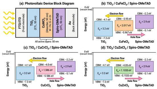
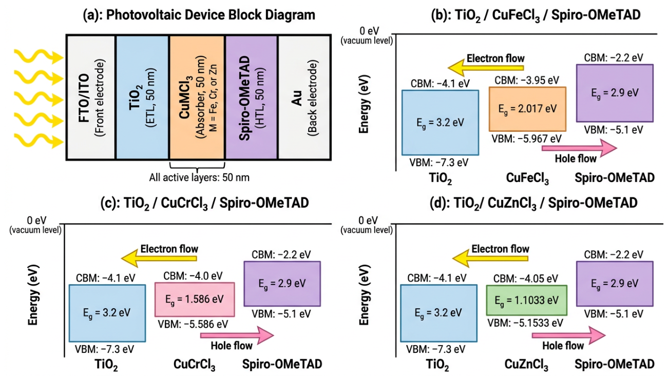
The bandgap, electron affinity, dielectric permittivity, effective density of states, carrier mobilities, doping, and defect density are the modelling characteristics summarized in Table 1 and Table 2 for each layer, based on values obtained in the literature [42,43,44,45,46,47,48,49,50,51,52,53,54]. CuMCl3 perovskites are not ambipolar; hence, their electron and hole mobilities should not be the same. We selected comparable mobility values (50 cm2/V·s for electrons and 40 cm2/V·s for holes) based on first-principles literature estimates. Okumura and Oku discovered that CuMCl3 crystals with Cr, Fe, or Cu as B-site cations have low effective mass ratios for electrons and holes, resulting in high carrier mobility for both charge carriers. The PDOS investigation showed charge transfer between the s, p, and d orbitals of Cu+ and the M2+ ion. Orbital overlap between Cu at the A-site and the MCl6 octahedron increased carrier mobility. Recent studies on CuGeCl3 and CuSnCl3 reveal electron and hole effective masses of 0.13 me/0.11 me and 0.22 me/0.33 me, showing balanced mobility in these systems. While we acknowledge that precise equality is an approximation, the figures are on the same order of magnitude and give a solid basis for SCAPS-1D simulation. We emphasized that these values are based on existing literature for CuMCl3 systems and not general assumptions [39,51,52,53,54]. In this configuration, SCAPS-1D is used to comprehensively analyze the performance of CuMCl3 across different metal perovskites (where M = Fe, Cr, Zn). Figure 1 shows the photovoltaic device’s schematic architecture, as well as energy level diagrams for the TiO2, CuFeCl3, CuCrCl3, and CuZnCl3 absorber layers interfaced with Spiro-OMeTAD. These diagrams show the band alignment and charge transport routes required to ensure optimal performance.
Figure 1.
(a) Device layer architecture consisting of FTO, TiO2, CuMCl3, Spiro-OMeTAD, and Au; (b) Energy band diagram of the device CuFeCl3 (TiO2/CuFeCl3/Spiro-OMeTAD); (c) Energy band diagram of the device CuFeCl3 (TiO2/CuCrCl3/Spiro-OMeTAD); (d) TiO2/CuZnCl3/Spiro-OMeTAD energy band diagram.
Several fabrication challenges of CuMCl3 perovskite absorbers must be resolved to ensure efficient device application. Phase stability is an important issue because Cu-based halides tend to undergo structural changes under ambient conditions. The emergence of competing phases like CuCl2 or secondary Cu-rich compounds can deteriorate the perovskite structure and its optoelectronic features. The synthesis should be performed in inert atmospheres and with controlled thermal annealing to promote the desired perovskite phase and to inhibit the growth of impurities. The oxidation of Cu+ to Cu2+ is a critical chemical instability problem since Cu+ is easily oxidized in air, resulting in the formation of CuO or CuCl2 phases that act as recombination centres and degrade the device’s performance. The +1-oxidation state can be maintained and oxidation reduced by protective encapsulating layers, synthesis under oxygen-free conditions, and the use of reducing chemicals or appropriate precursor stoichiometries. CuMCl3 materials are generally prepared by solid-state processes or solution-based methods such as antisolvent crystallization, spin-coating, or vapour deposition. The optimization of precursor ratio, reaction temperature, solvent choice, and annealing conditions is critical to obtain phase-pure and highly crystalline films, as they have a great influence on film morphology, defect density, and carrier transport [55].
Table 1.
The electrical, optical, and other material properties of TiO2, Spiro-OMeTAD transport layers, and CuMCl3 (M = Fe, Cr, and Zn) as a perovskite absorber used in these simulations are specified.
Table 2.
In all simulations, the same trap parameters were applied to the CuMCl3/TiO2 (absorber/ETL) and CuMCl3/Spiro-OMeTAD (absorber/HTL) interfaces [56,57,58,59,60].
Table 1 and Table 2 summarize the information entered for SCAPS-1D simulations, all sourced from previously published research [42,43,44,45,46,47,48,49,50,51,52,53,54]. The device’s constituent parts are TiO2, CuMCl3, and Spiro-OMeTAD. The 50 nm TiO2 layer has an electron transport gap of 3.2 eV and an electron affinity of 4.1 eV, whereas the 50 nm Spiro-OMeTAD layer has a hole transport gap of 2.9 eV. The bandgaps of CuFeCl3, CuCrCl3, and CuZnCl3 absorbers based on copper are 2.02, 1.59, and 1.10 eV, respectively. The electron affinities of these absorbers increase from 3.95 to 4.05 eV. The order-of-magnitude lower effective densities of states (Nc, Nv) for CuCrCl3 are 2.2 × 10¹⁷ and 1.8 × 1018 cm−3, respectively. All simulations and calculations reported in this work were carried out using the parameter values shown in Table 1.
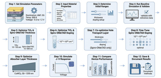
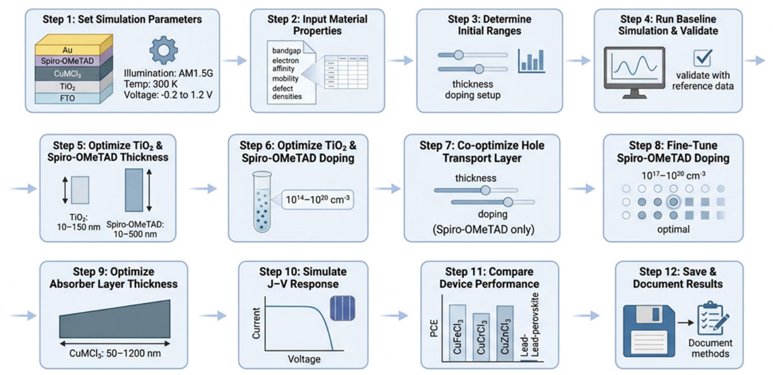
The SCAPS 1D simulation process, as illustrated in Figure 2, consists of a series of sequential actions that must be executed in order. Both TiO2 and Spiro-OMeTAD are tuned for thickness and doping density prior to the optimization of the perovskite absorber (CuMCl3) for each device, as detailed information about these sequential actions is provided in the Supplementary Materials.
Figure 2.
A conceptual simulation flow diagram for the optimization of TiO2/CuMCl3 (M = Fe, Cr, and Zn) devices used in the study.
The device optimization was performed by a sequential parametric approach, where the thickness and dopant concentration of each layer were optimized independently, fixing other parameters. The approach was applied to separate the effect of each variable in a systematic way and reduce the computational complexity. However, it is recognized that this sequential approach does not consider any possible interdependency of the parameters or global optimality, but provides a practical solution. Global optimization, though theoretically more efficient, is computationally and time-consuming, particularly when searching high-dimensional parameter spaces with multiple correlated variables, e.g., the thickness and doping of the electron and hole layers.
The results presented in this work are only numerical simulations with SCAPS-1D (version 3.8). SCAPS-1D is a known and verified software for solar device modelling. However, there are some assumptions inherent to the simulation framework that might affect the expected device performance. (i) The model assumes ideal contacts between the transport layers and the perovskite absorber and does not consider potential chemical reactions, interface defects, and changes in band offsets, which can affect charge extraction and recombination in real devices. (ii) The defect model employed is based on simplified Shockley–Read–Hall recombination parameters, not representative of the complex defect chemistry of copper-based perovskites, e.g., the possible formation of deep traps, defect migration, or defect–defect interactions under working conditions. (iii) The simulation assumes uniform doping and perfect charge carrier mobilities in the whole absorber layer, but real films often show spatial inhomogeneities, grain boundaries, and compositional variations, which can significantly affect the device performance. Effects of series and shunt resistances, which are important in real devices, were not explicitly modelled and may limit the fill factor and overall efficiency in experimental implementations. Thus, although our results provide significant theoretical insights and design principles for CuMCl3-based solar cells, they are predicted upper-bound performances and need to be experimentally validated. The quantitative efficiency numbers are to be seen as theoretical targets, not as experimental results [25,60].
3. Results and Discussion
3.1. Thickness Optimization of TiO2 as Electron Transport Layer
The TiO2 layer for electron transport in a planar n-i-p perovskite solar cell is responsible for blocking holes and removing photogenerated electrons from the CuMCl3 perovskite absorber. The ideal thickness of TiO2 in TiO2/CuMCl3/Spiro-OMeTAD cells strikes a compromise between electron extraction and series resistance. Shunting and recombination occur when the thickness is less than 10 nm, but transport length and trap-assisted recombination increase when the thickness exceeds 100 nm, leading to a decrease in fill factor and efficiency. By keeping parasitic losses to a minimum and optimizing coverage, a well-optimized layer may provide steady open-circuit voltage and high fill factor [43,46,57].
Before analyzing the device-level J-V response, it is necessary to define the particular material properties used for each perovskite absorber and the neighbouring charge-transport layers, since these inputs have a direct impact on the simulated photovoltaic metrics. SCAPS-1D defines key parameters for CuFeCl3, CuCrCl3, and CuZnCl3 absorbers, including bandgap, electron affinity, dielectric permittivity, effective density of states, carrier mobility, and defect density. Table 1 summarizes these parameters, as well as those of the TiO2 electron-transport layer (ETL) and the back contact. The effect of TiO2 ETL thickness on photovoltaic performance was investigated using fixed parameters.
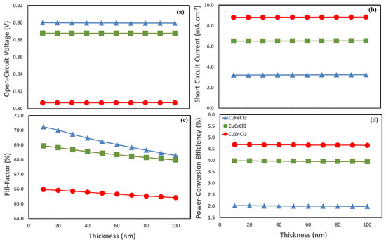
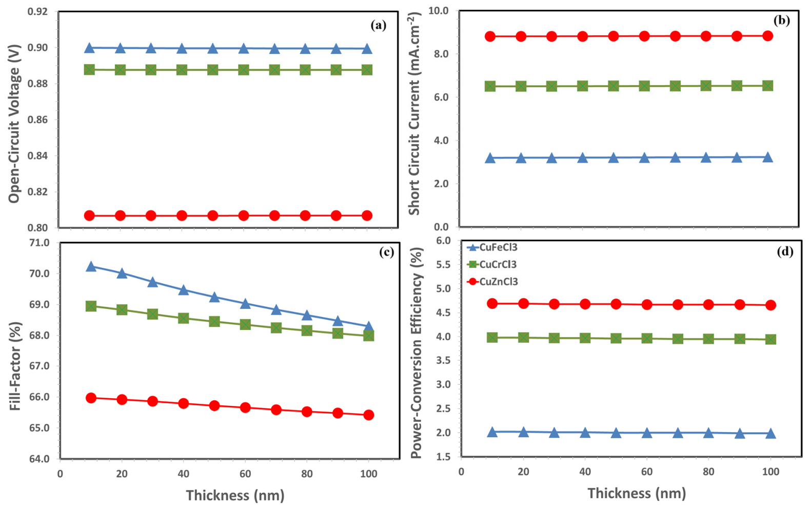
Figure 3 illustrates the principal photovoltaic characteristics as a function of TiO2 thickness, ranging from 10 to 100 nm. For all three perovskites, open-circuit voltage stays almost invariant with TiO2 thickness, suggesting bulk-limited recombination. Short-circuit current exhibits a marginal rise (nearly negligible) with thickness, indicating enhanced electron extraction, while fill factor decreases consistently because of escalating series resistance. CuZnCl3 exhibits the greatest short-circuit current (~8.8 mA·cm−2) but the lowest open-circuit voltage (~0.807 V), indicating a tighter bandgap; CuFeCl3 provides the highest open-circuit voltage (~0.900 V) at the cost of short-circuit current. The power-conversion efficiency reaches its peak for CuZnCl3 at around 4.7% (with 20 nm TiO2) and for CuFeCl3 at about 2.0% (with 20 nm TiO2), but CuCrCl3 exhibits an intermediate value of roughly 4.0% (with 25 nm TiO2). The ideal thickness is the lowest that prevents shunts, since thicker TiO2 consistently degrades the fill factor [61].
Figure 3.
Photovoltaic performance parameters: (a) Open-circuit voltage (), (b) short-circuit current density (), (c) fill factor (FF), and (d) power-conversion efficiency (PCE) of TiO2/CuMCl3/Spiro-OMeTAD devices (M = Fe, Cr, Zn) as a function of TiO2 thickness (0–100 nm).
3.2. Doping Optimization of TiO2 as Electron Transport Layer
Doping TiO2 has been shown to be an effective technique for minimizing the intrinsic defects of the electron transport layer in perovskite solar cells. Undoped TiO2 has inadequate electron mobility and a significant concentration of defect states, which limits device performance. Doping with elements such as niobium (Nb) or erbium (Er) has shown the capacity to enhance energy band alignment and reduce electronic trap states, thus promoting charge extraction. A self-doping technique using Ti3+ has been used to improve the synthesis and surface chemistry of TiO2 films. Co-doping with aluminum and magnesium (Al-Mg) improves electrical conductivity and optical transparency, attaining a maximum transmittance of 90% in the visible spectrum while preserving favourable band alignment with the perovskite absorber in most cases. These doping methods are crucial for improving the performance of solar cells [62,63,64].
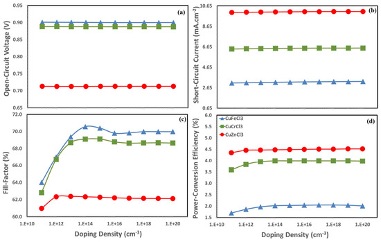
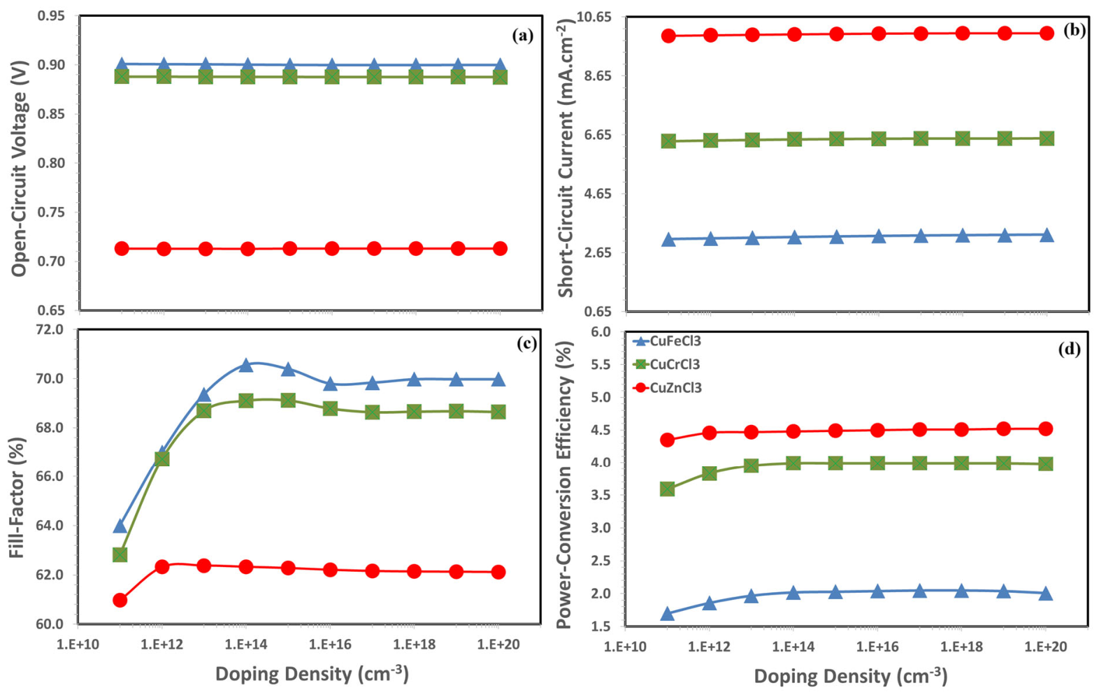
Figure 4 illustrates that the photovoltaic performance of perovskite solar cells with the TiO2/CuMCl3/Spiro-OMeTAD architecture is highly dependent on the doping concentration of the TiO2. As the doping density rises from 1 × 10¹¹ to 1 × 1020 cm−3, the short-circuit current increases monotonically owing to improved charge conductivity, whereas the open-circuit voltage remains relatively constant for CuZnCl3 (~0.713 V) and CuCrCl3 (~0.888 V) but experiences a slight decline for CuFeCl3 at elevated doping levels. The power-conversion efficiency reaches its maximum at around 1 × 10¹⁸–1 × 1019 cm−3 for all three samples, with CuZnCl3 attaining the greatest power-conversion efficiency (~4.5%) due to its better short-circuit current density and fill factor. Exceeding this doping level reduces the power-conversion efficiency, signifying a compromise between conductivity and recombination. Accurate adjustment of the doping in the TiO2 as the electron transport layer for Cu-based halide perovskite is crucial to optimize device performance.
Figure 4.
Photovoltaic performance parameters: (a) Ospen-circuit voltage (), (b) short-circuit current density (), (c) fill-factor (FF), and (d) power-conversion efficiency (PCE) of TiO2/CuMCl3/Spiro-OMeTAD devices (M = Fe, Cr, Zn) as a function of TiO2 doping density (1011–1020 cm−3).
Open-circuit voltage and short-circuit current exhibit invariant behaviour with TiO2 doping, resulting in a significant rise in fill-factor, which is physically justified.
External electron-transport layer doping has little effect on the CuMCl3 absorber’s bulk recombination kinetics or bandgap, which primarily determine open-circuit voltage. Similarly, short-circuit current is intrinsically limited by photon absorption and carrier generation in the absorber; nevertheless, under short-circuit conditions, charge extraction is very effective and unaffected by tiny doping changes. Fill factor is very sensitive to series resistance, interfacial recombination, and charge extraction efficiency, all of which are directly impacted by TiO2 doping. Augmented doping improves TiO2 conductivity, reduces series resistance, optimizes band alignment at the TiO2/CuMCl3 interface, and reduces interfacial recombination, leading to a higher fill factor. As a result, whereas open-circuit voltage and short-circuit current are determined by the absorber’s intrinsic properties, the fill factor is impacted by transport layer characteristics, shedding light on the doping-dependent patterns seen.
3.3. Thickness Optimization of Spiro-OMeTAD as Hole Transport Layer
Optimizing the thickness of Spiro-OMeTAD is essential for maintaining the critical compromise between interfacial quality and charge transport efficiency [65]. (a) Interfacial Recombination: Insufficient layer thickness often leads to poor morphological coverage of the electrode and/or perovskite heterojunctions. These imperfections enable direct shunt paths and localized recombination at the cathode contact, resulting in a considerable drop in open-circuit voltage. Localized defects impair the electron-blocking function, resulting in increased non-radiative recombination losses [66,67,68]. (b) Transport Resistance and Extraction: Enhanced hole-transport layer thickness elevates bulk transport resistance, hence diminishing both fill factor and short-circuit current density due to impeded carrier extraction. (c) Non-uniform doping: Moreover, high thickness fosters non-uniform doping and oxidation gradients, possibly attributable to trapped solvent species or dopant movement.
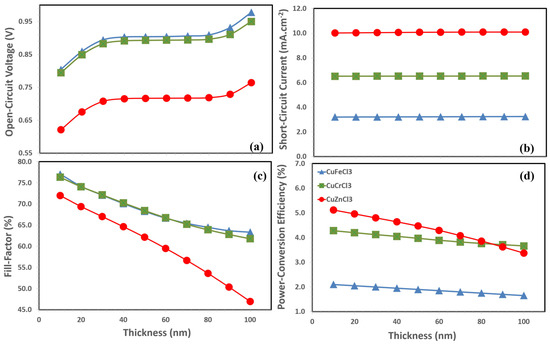
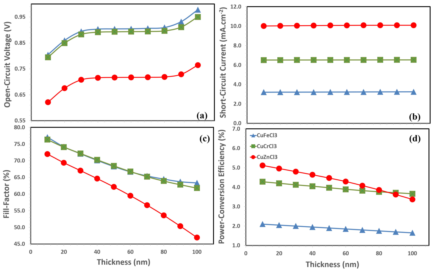
The thorough examination of Spiro-OMeTAD thickness in Figure 5 reveals significantly different thickness–response correlations for CuFeCl3, CuCrCl3, and CuZnCl3, respectively. All devices demonstrate a uniform reduction in fill factor and power-conversion efficiency with increasing thickness. The optimum Spiro-OMeTAD thickness for several device configurations is determined to be 10 nm, supported by documented trends in the perovskite/HTM literature [69].
Figure 5.
Photovoltaic performance parameters: (a) Open-circuit voltage (), (b) short-circuit current density (), (c) fill-factor, and (d) power-conversion efficiency (PCE) of TiO2/CuMCl3/Spiro-OMeTAD devices (M = Fe, Cr, Zn) as a function of Spiro-OMeTAD thickness (10–100 nm).
For CuFeCl3, the open-circuit voltage remains reasonably steady, ranging from 0.9039 to 0.8778 as the parameter grows from 10 to 100, but the short-circuit current exhibits a continuous increase from 3.0147 to 3.6182. Nonetheless, this increment fails to compensate for the decline in fill factor (from 77.06 to 63.35), culminating in a marginal reduction in power conversion efficiency (from 2.10 to 2.00). In contrast, CuCrCl3 exhibits an increased transport gain in short-circuit current (6.2731 → 6.8162), with a substantial decrease in fill-factor (76.34 → 61.80) and a notable loss in power-conversion efficiency (4.28 → 3.66), whereas open-circuit voltage stays rather stable up to 80 nm before decreasing (0.8929 → 0.8682 at 100). CuZnCl3 has the most sensitivity to thickness: although short-circuit current increases somewhat (9.9171 → 10.1463), fill-factor experiences a substantial loss (71.99 → 46.96), and open-circuit voltage simultaneously decreases (0.7167 → 0.7082), culminating in the most significant reduction in power-conversion efficiency (5.12 → 3.37).
3.4. Doping Optimization of Spiro-OMeTAD as Hole Transport Layer
Improving the acceptor doping of Spiro-OMeTAD as a hole transport layer is crucial for reducing interfacial recombination and promoting efficient charge extraction in the advancement of the photovoltaic response of perovskite solar cells. Apart from the exceptional electrical and photovoltaic characteristics of Spiro-OMeTAD, along with its film uniformity, significant acceptor doping is essential to improve the intrinsic conductivity of Spiro-OMeTAD [70]. Recent studies indicate that optimizing acceptor doping of Spiro-OMeTAD may further enhance the internal electric field and reduce dark current, which, in turn, improves the band alignment at the interface for efficient photovoltaic responses [71,72].
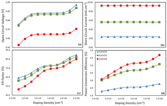
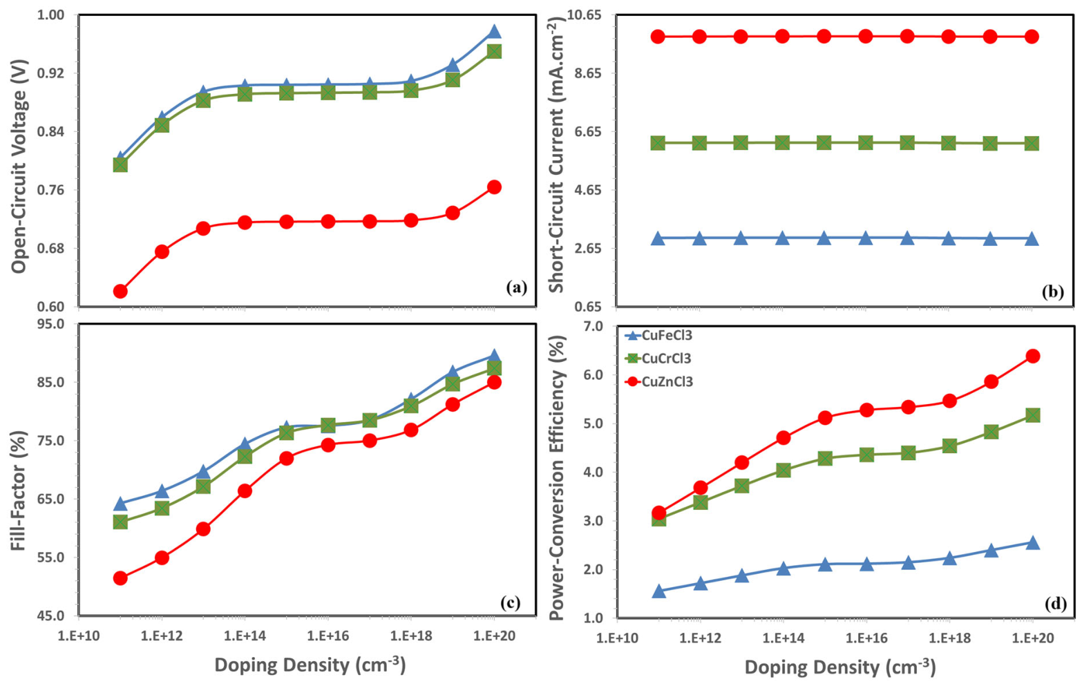
The photovoltaic responses of CuFeCl3, CuCrCl3, and CuZnCl3 with Spiro-OMeTAD doping density (1 × 10¹¹ to 1 × 1020 cm−3) are shown in Figure 6. The figures exhibit distinct trade-offs governed by charge transport and recombination mechanisms. In all the above devices, increased doping elevates the conductivity of the hole transport layer (HTL), modifies the quasi-Fermi level of holes, and reduces interfacial recombination, hence consistently improving the fill factor and open-circuit voltage. In contrast, the short-circuit current shows fluctuating responses: CuZnCl3 generates the maximum short-circuit current (~9.9 mA/cm2), attributable to perfect band alignment between the absorber and hole-transport layer, together with reduced parasitic absorption. On the other hand, CuFeCl3 yields the lowest short-circuit current (~3.0 mA/cm2), likely resulting from accelerated carrier recombination at the TiO2/absorber interface. CuCrCl3 exhibits an intermediate short-circuit current of around 6.3 mA/cm2. At optimal doping (1 × 1020 cm−3), CuZnCl3 achieves a maximum power conversion efficiency of 6.39% due to its increased short-circuit current density and improved open-circuit voltage of 0.764 V. CuCrCl3 achieves a power conversion efficiency of 5.17% with a moderate open-circuit voltage of 0.950 V; CuFeCl3 exhibits worse performance at 2.56%, although it has the greatest open-circuit voltage of 0.978 V, limited by inadequate short-circuit current. This underscores that acceptor optimization at 1020 cm−3 must balance doping-induced increases in open-circuit voltage and fill factor against short-circuit current reductions caused by excessive recombination or mobility variations for all devices.
Figure 6.
Photovoltaic performance parameters: (a) Open-circuit voltage (), (b) short-circuit current density (), (c) fill-factor (FF), and (d) power-conversion efficiency (PCE) of TiO2/CuMCl3/Spiro-OMeTAD devices (M = Fe, Cr, Zn) as a function of Spiro-OMeTAD doping density (1011–1020 cm−3).
3.5. Thickness Optimization of CuMCl3 (M = Fe, Cr and Zn) as Absorber
Optimizing the thickness of the perovskite absorber layer is essentially a multi-objective challenge that balances optical absorption, charge generation, charge recombination, and charge transport dynamics, which significantly influences total photovoltaic efficiency. A thicker layer (e.g., >1000 nm) improves photon absorption and the production of electron–hole pairs, resulting in an increased short-circuit current density. However, increasing the thickness beyond the charge carrier diffusion length dramatically elevates the likelihood of bulk recombination. This leads to considerable reductions in the fill factor and the open-circuit voltage prior to the extraction of charges at the electrodes. Thus, the power conversion efficiency exhibits a non-monotonic trend, reaching its maximum within a certain thickness range, often between 400 nm and 900 nm, depending upon the perovskite composition. Consequently, rigorous optimization of absorber thickness is crucial to reduce recombination losses and enhance photon absorption, thus facilitating the design of highly efficient perovskite solar cells [73,74,75].
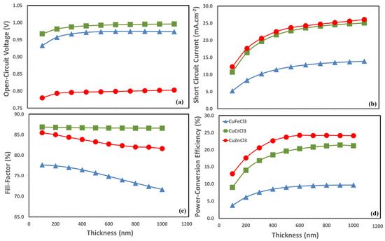
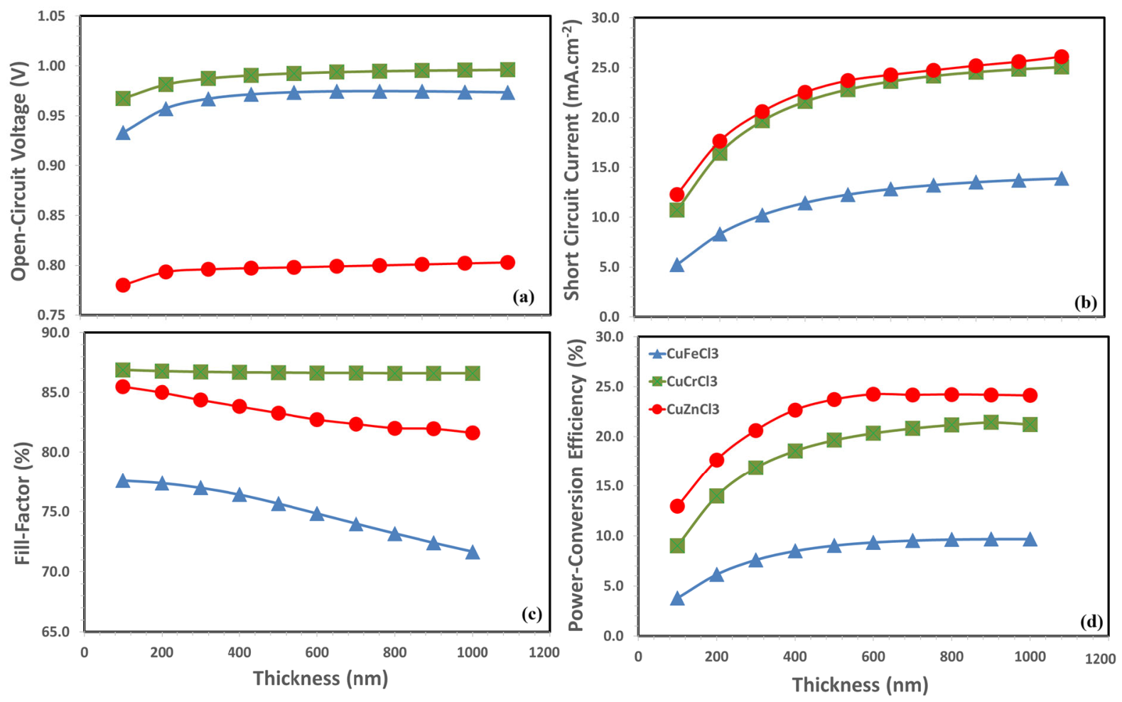
Figure 7 systematically compares the photovoltaic performance of CuFeCl3, CuCrCl3, and CuZnCl3 devices in relation to absorber thickness. CuCrCl3 demonstrates an excellent combination of higher open-circuit voltage (reaching 0.99 V), remarkable fill factor (approximately 86.6%), and significant short-circuit current density (attaining 25.06 mA cm−2), resulting in a maximum power conversion efficiency of 21.4% at 900 nm with minimal roll-off beyond 800 nm. The thickness-tolerant behaviour arises from a favourable direct bandgap (~1.59 eV), a high dielectric constant (εᵣ = 5.2) that reduces charged defects, and an extended minority-carrier diffusion length, which together inhibit Shockley–Read–Hall recombination even in substantial absorbers [76]. Conversely, CuZnCl3 attains an extraordinarily high short-circuit current density (>38 mA cm−2) and a peak efficiency of 24.2% at about 700 nm, although it experiences a much lower open-circuit voltage (~0.79 V) and a pronounced reduction in fill factor with increased film thickness. The higher photocurrent correlates with a reduced bandgap (~1.10 eV) that broadens light absorption; however, the voltage deficit is intensified by a substantial concentration of shallow acceptors (due to Zn2+ substitution) and diminished electron mobility, which facilitates trap-assisted Auger recombination and diffusion-limited collection beyond the ~300 nm diffusion length. CuFeCl3 exhibits significant underperformance, achieving a maximum efficiency of just 9.7%, despite a respectable open-circuit voltage (~0.97 V); its short-circuit current density consistently stays below 14 mA cm−2, and the fill factor progressively declines from 77.6% to 71.7% as thickness increases. The subpar performance is ascribed to deep Fe3+/Fe2+ redox states that produce mid-gap traps, leading to an extremely short carrier lifetime (<1 ns) and a diffusion length under 100 nm, causing the majority of photogenerated carriers to recombine prior to extraction [76,77]. Figure 7 together demonstrates a distinct trade-off: CuCrCl3 provides balanced, thickness-tolerant performance, whereas CuZnCl3 attains record photocurrent at the cost of voltage—an essential consideration for the design of next-generation halide photovoltaics.
Figure 7.
Photovoltaic performance parameters: (a) Open-circuit voltage (), (b) short-circuit current density (), (c) fill-factor (FF), and (d) power-conversion efficiency (PCE) of TiO2/CuMCl3/Spiro-OMeTAD devices (M = Fe, Cr, Zn) as a function of absorber layer thickness (100–1000 nm).
It is important to note that the optimized performance of each CuMCl3 device arises from complex interdependencies among parameters. Absorber thickness couples with transport layer doping, while cation choice (Fe, Cr, Zn) influences optimal ETL thickness via dielectric constant and diffusion length. Understanding these trade-offs is essential for experimental realization [60,76].
3.6. Optimized Layer Parameters and Performance Summary
Table 3 displays the optimized device parameters for CuFeCl3, CuCrCl3, and CuZnCl3, respectively. All devices use an undoped absorber and a highly p-doped Spiro-OMeTAD hole transport layer (10 nm, 1 × 1020 cm−3). Variations in performance stem from the parameters of the TiO2 electron transport layer (ETL) and the characteristics of the absorber. The ultra-short diffusion length of CuFeCl3 (PCE = 9.7%) is compensated for by a thick TiO2 (25 nm, 1 × 1018 cm−3); however, interfacial recombination is increased. CuCrCl3 (21.4%) utilizes a thinner, more heavily doped TiO2 (20 nm, 1 × 1019 cm−3), minimizing parasitic absorption and aligning with its thickness (~900 nm). On the other hand, excessive Spiro p-doping somewhat constrains the fill factor. CuZnCl3 attains maximum efficiency (24.2%) with similar TiO2 configurations (20 nm, 1 × 1019 cm−3) and a consistent Spiro-OMeTAD layer. Its advantage arises from a reduced bandgap (~1.10 eV) that facilitates increased photocurrent, together with an ideal absorber thickness (700 nm) that reconciles absorption and bulk recombination. Consequently, the electrical characteristics of the absorber, rather than only the fluctuations in the transport layer, dictate the optimal device performance [76,77].
Table 3.
Shows optimized layer specifications in terms of thickness and doping density for devices CuFeCl3, CuCrCl3, and CuZnCl3, respectively.
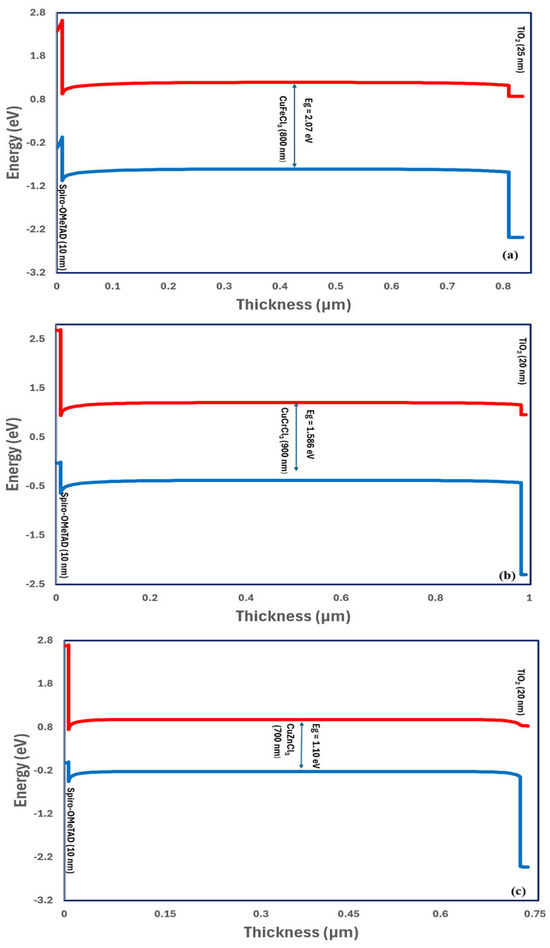
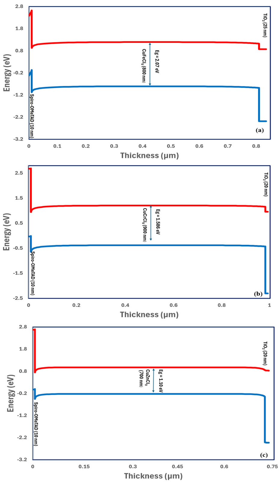
Figure 8 presents the energy band diagrams at equilibrium for optimized CuFeCl3, CuCrCl3, and CuZnCl3 devices, showing conduction band minimum (CBM) and valence band (VBM) alignment throughout the FTO/TiO2/CuMCl3/Spiro-OMeTAD/Au stack. Fixed energy positions in the transport layer are constant, while absorber levels (a–c) reflect their distinct bandgaps and electron affinities. All devices employ a 10 nm heavily p-doped Spiro-OMeTAD HTL (1 × 1020 cm−3) and TiO2 ETL optimized at 20–25 nm (1 × 10¹⁸–1 × 1019 cm−3). The TiO2/CuMCl3 conduction band offset critically governs electron extraction. CuFeCl3 has a larger CBO that assists injection but causes more interfacial recombination due to its ultrashort diffusion length (~100 nm), requiring a thicker 25 nm ETL. On the other hand, CuCrCl3 and CuZnCl3 are properly aligned, which lets us use thinner 20 nm ETLs to lower unwanted losses. The valence band offset of CuMCl3/the Spiro interface is large enough to extract holes in all devices, although the high p-doping of Spiro slightly limits the fill factor of CuCrCl3. The lower bandgap of CuZnCl3 (~1.10 eV) results in a higher VBM, which is beneficial for generating more photocurrent and improving the collection of holes. The 700 nm absorber thickness for CuZnCl3 is the best compromise between absorption and bulk recombination losses, unlike the thicker absorber in CuFeCl3 that increases losses. This analysis indicates that absorber-intrinsic properties such as bandgap and defect tolerance are more important for performance than transport layer engineering.
Figure 8.
Energy band diagram of the optimized devices: (a) CuFeCl3, (b) CuCrCl3, and (c) CuZnCl3.
3.7. Comparative Current–Voltage Characteristics of the Optimized Devices
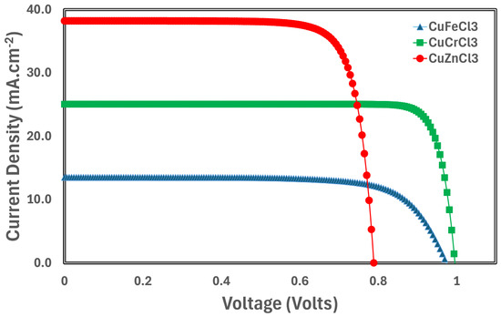
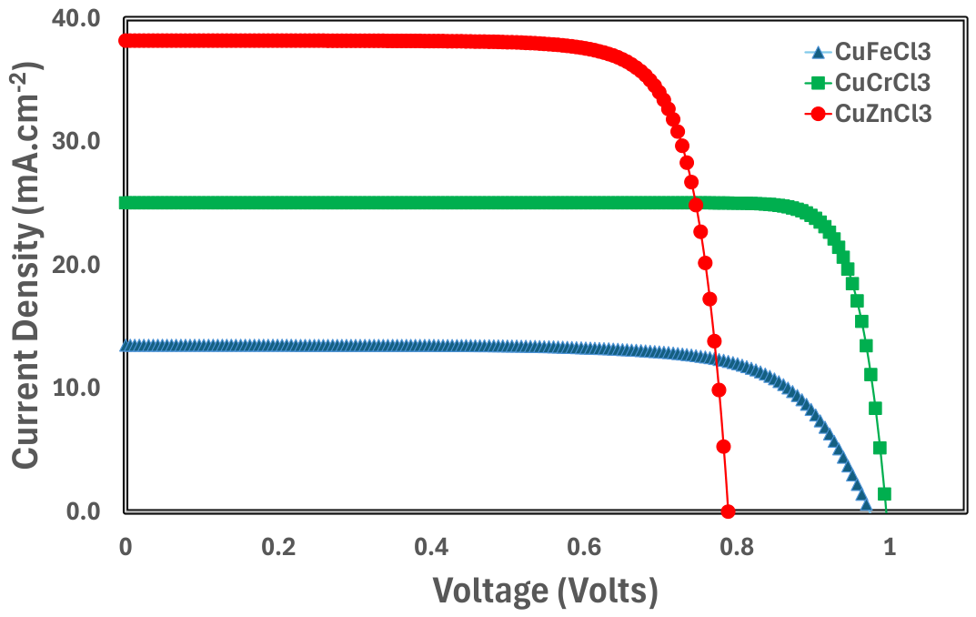
Figure 9 illustrates the current–voltage characteristics of the fully optimized devices CuFeCl3, CuCrCl3, and CuZnCl3 under AM1.5G illumination. Table 4 presents a summary of the photovoltaic responses such as open-circuit voltage, short-circuit current, fill factor, and power conversion efficiency for each of the highly optimized devices. The CuZnCl3 device has the greatest short-circuit current density (38.2 mA cm−2), attributable to its narrow bandgap (~1.10 eV), which enhances near-infrared harvesting. The open-circuit voltage is just 0.79 V, indicating considerable trap-driven recombination due to Zn-induced shallow acceptors and a limited diffusion length. At the ideal thickness of 700 nm, the fill factor attains 80.2% but diminishes with increasing film thickness owing to electrode recombination. The CuCrCl3 device exhibits balanced performance, with a short-circuit current of 25.1 mA cm−2, an open-circuit voltage of 0.99 V, and a steady fill factor of around 86.15% throughout a broad thickness range. Extended diffusion lengths and an elevated dielectric constant diminish non-radiative recombination. CuFeCl3 is constrained by profound Fe3+/Fe2+ traps, leading to a moderate open-circuit voltage (0.95 V), a low short-circuit current (13.3 mA cm−2), and a rapidly decreasing fill factor (77.1%). This results in a modest power conversion efficiency of 9.7%. The current–voltage curves indicate a distinct trade-off: CuZnCl3 enhances photocurrent at the cost of voltage, while CuCrCl3 provides superior voltage and fill factor. Notwithstanding its reduced open-circuit voltage, the CuZnCl3 device attains a remarkable efficiency of 24.2%. This results from its enhanced short-circuit current and ideal absorber thickness (700 nm), which equilibrates absorption and recombination [78,79,80].
Figure 9.
Optimized current–voltage characteristics of CuFeCl3, CuCrCl3, and CuZnCl3 devices. Table 4 highlights the most significant performance metrics, including open-circuit voltage, short-circuit current, fill factor, and power conversion efficiency.
Table 4.
Summary of the photovoltaic responses such as open-circuit voltage, short-circuit current, fill factor, and power conversion efficiency for each of the highly optimized devices.
3.8. Temperature Dependence of Photovoltaic Performance of Optimized Devices
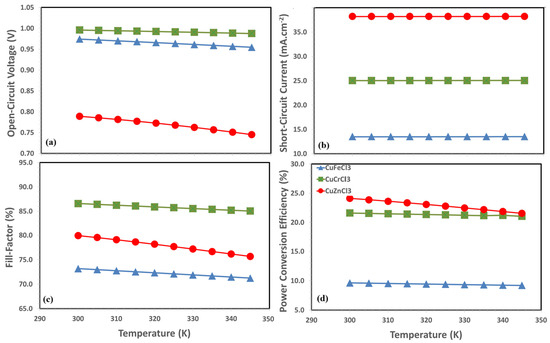
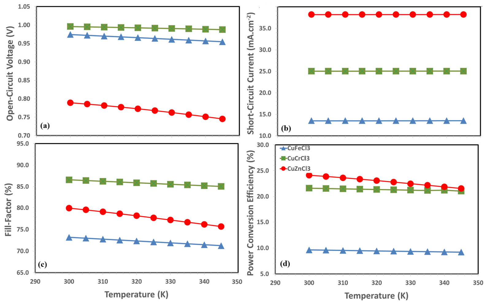
Figure 10 shows the thermal performance of photovoltaic parameters in the TiO2/CuMCl3/Spiro-OMeTAD devices, where M = Fe, Cr, Zn, at 300–345 K. Power conversion efficiency declines monotonically with temperature across all three devices, as do other photovoltaic parameters such as open-circuit voltage, short-circuit current, and fill factor, although with dramatically different slopes. The CuZnCl3 device has the best initial power-conversion efficiency (24.2% at 300 K), but suffers a significant drop, losing around 2.5 percent by 345 K. The CuCrCl3 device shows moderate stability (21.4% → 21.05%), while the CuFeCl3 device, though lowest in absolute efficiency (9.7% → 9.20%), has the weakest thermal sensitivity [81,82,83,84].
Figure 10.
Temperature-dependent photovoltaic performance (a) open-circuit voltage, (b) short-circuit current, (c) fill-factor, and (d) power-conversion efficiency of CuFeCl3, CuCrCl3, and CuZnCl3 devices assessed from 300 K to 345 K under AM1.5G illumination.
3.9. Trap-Mediated Comparative Deterioration of Photovoltaic Response of the Optimized Devices
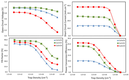
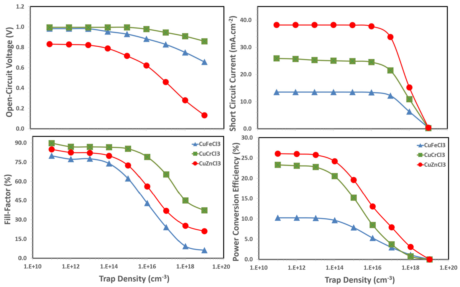
Figure 11 demonstrates a consistent decline in all photovoltaic parameters when trap density (Nt) increases from 1011 to 1019 cm−3 at 300 K. The universal trend for CuFeCl3, CuCrCl3, and CuZnCl3 indicates that the degradation severity at a constant Nt is ranked as follows: CuZnCl3 > CuCrCl3 > CuFeCl3. This sensitivity results from variations in defect formation energetics and charge-carrier capture cross-sections. The existence of open-shell Fe3+ in CuFeCl3 creates deep trap states that saturate at moderate trap density, thereby restricting further non-radiative recombination; hence, its open-circuit voltage is comparatively elevated (0.78 V at 1016 against 0.70 V for CuZnCl3 at the same Nt). In contrast, CuZnCl3 displays shallow, delocalized traps associated with Zn2+-related halide vacancies, functioning as effective Shockley–Read–Hall centres. CuCrCl3 demonstrates intermediate behaviour owing to the Jahn–Teller distortion of Cr3+, which generates anisotropic trap distributions that partially alleviate recombination. At Nt > 1018 cm−3, all devices reach the trap-filled limit, where space-charge-limited currents prevail, and power conversion efficiency approaches < 1%. The findings quantitatively demonstrate that trap density, influenced by the M-site cation, determines the maximum efficiency limit at ambient temperature [85,86,87,88].
Figure 11.
Trap-mediated photovoltaic degradation of CuFeCl3, CuCrCl3, and CuZnCl3 devices assessed from 1011 to 1020 cm−3 at room temperature under AM1.5G illumination.
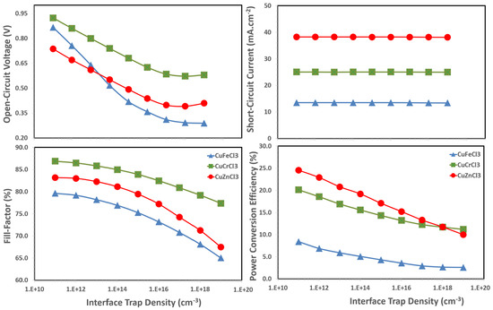
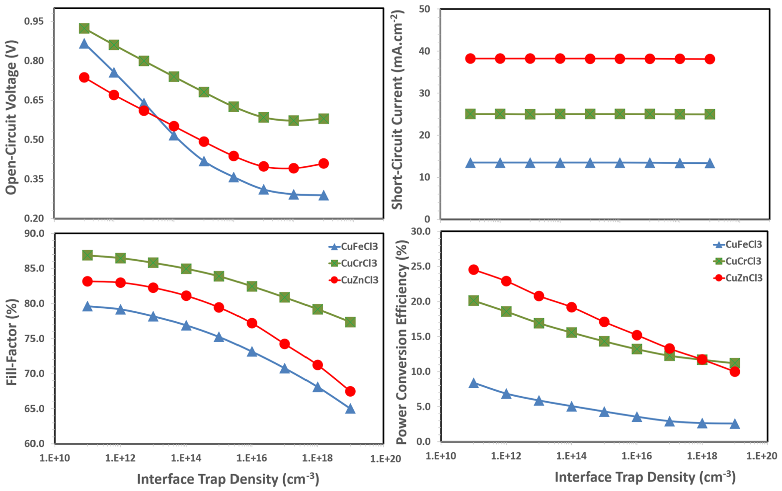
To improve interfacial passivation, it is crucial to examine how interface trap density at the CuMCl3/transport layer junction affects open-circuit voltage and fill factor, since bulk trap density degrades device performance. Figure 12 shows the behaviour of the photovoltaic responses of devices as a function of interface trap states between the charge transport layer (hole-transport layer) and the CuMCl3 absorber layer (for simplicity, as a very similar trend is observed between the electron-transport layer and the CuMCl3 absorber layer). The figure shows a significant and consistent degradation in the open-circuit voltage, fill factor, short-circuit current, and power-conversion efficiency as the density of interface traps increases from 1 × 10¹¹ to 1 × 1019 cm−3. These interface traps might operate as a source of recombination centers, allowing non-radiative Shockley–Read–Hall (SRH) recombination. This recombination process immediately reduces the quasi-Fermi level separation, resulting in a reduction in open-circuit voltage and a decrease in charge extraction that contributes to the reduction in fill factor [89].
Figure 12.
Interface trap density-mediated photovoltaic degradation at the transport layer/CuMCl3 interface, assessed for CuFeCl3, CuCrCl3, and CuZnCl3 devices over a trap density range of 1011 to 1019 cm−3 at room temperature under AM1.5G illumination.
Defects formed at grain boundaries and surfaces of CuMCl3 perovskites act as non-radiative recombination sites, leading to deep trap states, which reduce the open-circuit voltage and efficiency. Such defects also encourage oxidation of Cu+ and migration of ions, which decreases stability. The passivation techniques, such as Lewis acid-base treatments, coordination with organic molecules, and 2D/3D heterostructures, can efficiently reduce recombination and improve performance. Future experiments should focus on defect engineering to fully realize the expected photovoltaic potential [89].
3.10. Benchmarking of Device Performance
The CuMCl3 absorbers cannot be directly compared to current copper-based perovskites due to chemical compositional changes (mixed-halide or double-perovskite types) and device fabrication discrepancies [85,90,91,92]. Nonetheless, the data in Table 5 offer a reasonable basis for comparison. In the table, the highest power conversion efficiency for a copper-based perovskite is 26.05% for Cs2CuBiCl6. The CuFeCl3 device achieves a power conversion efficiency of 9.7%, while the CuCrCl3 and CuZnCl3 devices achieve efficiencies of 21.4% and 24.2%, respectively, values that are comparable to the leading lead-free copper-based perovskite solar cells. This performance is coupled with open-circuit voltages of 0.99 V (for CuCrCl3), short-circuit currents of 38.2 mA·cm−2 (for CuZnCl3), and fill factors of over 80%, indicating effective charge extraction and low recombination losses.
Table 5.
Shows photovoltaic characteristics for CuMCl3 (M = Fe, Cr, Zn) perovskites compared to published lead-free Cu-based perovskite solar cells. Where HTL: hole-transport layer, ETL: electron-transport layer, Voc: open-circuit voltage, JSC: short-circuit current, FF: fill factor, PCE: power-conversion efficiency.
Although progress has been made in lead-free perovskite photovoltaics using tin, bismuth, and antimony-based systems, these materials still face fundamental limitations such as Sn oxidation instability, low-dimensional charge transport bottlenecks, and suboptimal bandgap tuning. Copper(I) perovskite chlorides (CuMCl3, where M = Fe, Cr, Zn) represent a promising alternative direction in lead-free absorber design. However, no complete theoretical analysis has investigated their photovoltaic potential. This research identifies four distinct levels of innovation that push the field beyond the current state-of-the-art altogether. To the best of our knowledge, we present the first systematic SCAPS-1D simulation framework for CuMCl3 perovskites, providing a theoretical foundation missing in the literature. Our work simultaneously evaluates three compositions (CuFeCl3, CuCrCl3, CuZnCl3) and achieves acceptable efficiencies of 24.2% for CuZnCl3 and 21.4% for CuCrCl3, respectively. Second, this paper provides the first numerical study of how different cations affect the performance trade-offs in copper(I) perovskite chlorides. We demonstrate that Zn2+ substitution enables an exceptionally high short-circuit current (38.2 mA·cm−2) due to bandgap narrowing (1.10 eV), while Cr3+ substitution yields a superior fill factor (86.15%) and thermal stability—a compositional engineering insight that offers some design rules for optimizing specific photovoltaic metrics.
These contributions represent a reasonable departure from previous works, which have been limited to (i) individual copper perovskite compositions with low efficiency, (ii) experimental synthesis without systematic theoretical guidance, (iii) qualitative stability observations, and (iv) narrow optimization scopes that ignore the critical interplay between absorber properties and transport layer engineering. We have taken a comprehensive approach for high-efficiency, lead-free CuMCl3 photovoltaics, including bandgap engineering, transport layer engineering, defect physics, and thermal stability. This work offers a useful theoretical perspective on copper-based perovskite solar cells and could contribute, in part, to their ongoing development toward practical applications.
4. Conclusions
The study successfully optimized three copper(I) perovskite chlorides, CuFeCl3, CuCrCl3, and CuZnCl3, as lead-free absorbers for the TiO2/CuMCl3/Spiro-OMeTAD device architecture using SCAPS-1D simulations. The findings indicate that cation substitution at the M-site substantially influences photovoltaic performance and stability. The CuZnCl3 device had a peak power conversion efficiency of 24.2%, owing to its narrow bandgap (~1.10 eV) and very high short-circuit current (38.2 mA·cm−2), despite a comparatively low open-circuit voltage (0.79 V) resulting from shallow acceptor-induced recombination. The CuCrCl3 device exhibited a remarkable performance of 21.4%, accompanied by an exceptional fill factor of 86.2% and thermal stability, while the CuFeCl3 device was constrained by substantial Fe3+/Fe2+ traps, resulting in a performance of 9.7%. The temperature-dependent study showed that CuZnCl3 exhibits the highest thermal sensitivity, whereas CuFeCl3 shows the lowest thermal sensitivity. Elevating trap density above 1018 cm−3 pushes all devices into the trap-filled domain, diminishing efficiency to below 1%. A comparison of tested lead-free copper-based perovskites shows that CuCrCl3 and CuZnCl3 are better than the current options.
Although these results show the theoretical expectations of the SCAPS-1D simulations under ideal conditions, they should be carefully interpreted for practical viability. The predicted efficiencies of 24.2% for CuZnCl3 and 21.4% for CuCrCl3 are higher than the experimentally measured efficiencies for similar Cu-based perovskites. This mismatch highlights the tremendous challenges that need to be overcome to successfully translate these predictions into working devices, such as the growth of phase-pure CuMCl3 films with the correct stoichiometry, effective defect passivation, and improved interface engineering. Our extensive optimization provides a clear roadmap by specifying ideal thicknesses, doping concentrations, and layer topologies to focus experimental efforts toward fully realizing the promise of CuMCl3 perovskites. These theoretical predictions need to be validated by future experimental synthesis, interface passivation, and large-scale manufacturing to bridge the gap between simulation and real device performance.
Supplementary Materials
The following supporting information can be downloaded at: https://www.mdpi.com/article/10.3390/cryst16090596/s1. The detailed simulation workflow, illustrated in Figure 2, is provided as Supplementary Material via the link above. Section S1: Simulation Steps; Section S2: Determination of Optical Absorption Coefficient of CuFeCl3 (Eg = 2.02 eV); Section S3: Determination of Optical Absorption Coefficient of CuCrCl3 (Eg= 1.59 eV); Section S4: Determination of Optical Absorption Coefficient of CuZnCl3 (Eg = 1.1 eV); Section S5: Validation Approach.
Author Contributions
All coauthors (S.A.M., M.S.A. and A.N.M.A.) share the same responsibility for conceptualization, methodology, software, validation, formal analysis, investigation, resources, data curation, writing—original draft preparation, writing—review and editing, visualization, supervision, and project administration. All authors have read and agreed to the published version of the manuscript.
Funding
This research work was funded by Umm Al-Qura University, Saudi Arabia, under grant number: 26UQU4330024GSSR03.
Data Availability Statement
Data is available on request.
Acknowledgments
The authors extend their appreciation to Umm Al-Qura University, Saudi Arabia for funding this research work through grant number: 26UQU4330024GSSR03.
Conflicts of Interest
The authors declare no conflicts of interest.
References
- Zheng, Y.; Li, Y.; Zhuang, R.; Wu, X.; Tian, C.; Sun, A.; Chen, C.; Chen, C.; Guo, Y.; Hua, Y.; et al. Towards 26% efficiency in inverted perovskite solar cells via interfacial flipped band bending and suppressed deep-level traps. Energy Environ. Sci. 2023, 17, 1153–1162. [Google Scholar] [CrossRef] [Scilit]
- Castriotta, L.A. Entering the 27% era: Practical design rules for Single-Junction Perovskite Solar Cells. ACS Energy Lett. 2026, 11, 2378–2381. [Google Scholar] [CrossRef] [Scilit] [PubMed]
- Li, C.; Lu, X.; Ding, W.; Feng, L.; Gao, Y.; Guo, Z. Formability of ABX 3 (X = F, Cl, Br, I) halide perovskites. Acta Crystallogr. Sect. B Struct. Sci. 2008, 64, 702–707. [Google Scholar] [CrossRef] [Scilit] [PubMed]
- Deng, X.; Chen, J.; Luo, Q. Prediction of ABX3 perovskite crystal structure based on random forest algorithm. Multiscale Multidiscip. Model. Exp. Des. 2025, 9, 40. [Google Scholar] [CrossRef] [Scilit]
- Zhang, W.; Liu, H.; Yan, F.; Dong, B.; Wang, H. Recent progress of Low-Toxicity Poor-Lead All-Inorganic perovskite solar cells. Small Methods 2023, 8, e2300421. [Google Scholar] [CrossRef] [Scilit] [PubMed]
- Moiz, S.A.; Alahmadi, A.N.M.; Aljohani, A.J. Design of a novel Lead-Free Perovskite solar cell for 17.83% efficiency. IEEE Access 2021, 9, 54254–54263. [Google Scholar] [CrossRef] [Scilit]
- Poli, I.; Gatti, T.; Li, Y.; Agresti, A.; Castriotta, L.A.; De Rossi, F.; Shukla, S.; Aernouts, T.; Eslava, S.; Malavasi, L.; et al. Lead-free perovskites and derivatives for photogeneration: A roadmap to sustainable approaches for photovoltaics and photo(electro)catalysis. J. Phys. Energy 2025, 8, 011501. [Google Scholar] [CrossRef] [Scilit]
- Shockley, W.; Queisser, H.J. Detailed balance limit of efficiency of p-n junction solar cells. J. Appl. Phys. 1961, 32, 510–519. [Google Scholar] [CrossRef] [Scilit]
- Rühle, S. Tabulated values of the Shockley–Queisser limit for single junction solar cells. Sol. Energy 2016, 130, 139–147. [Google Scholar] [CrossRef] [Scilit]
- Rong, Y.; Hu, Y.; Mei, A.; Tan, H.; Saidaminov, M.I.; Seok, S.I.; McGehee, M.D.; Sargent, E.H.; Han, H. Challenges for commercializing perovskite solar cells. Science 2018, 361, eaat8235. [Google Scholar] [CrossRef] [Scilit] [PubMed]
- Tong, X.; Lin, F.; Wu, J.; Wang, Z.M. High performance perovskite solar cells. Adv. Sci. 2015, 3, 1500201. [Google Scholar] [CrossRef] [Scilit] [PubMed]
- Jin, Z.; Zhang, Z.; Xiu, J.; Song, H.; Gatti, T.; He, Z. A critical review on bismuth and antimony halide based perovskites and their derivatives for photovoltaic applications: Recent advances and challenges. J. Mater. Chem. A 2020, 8, 16166–16188. [Google Scholar] [CrossRef] [Scilit]
- Moiz, S.A.; Alahmadi, A.N.M.; Alshaikh, M.S. Lead-Free FACSSNI3 based Perovskite Solar Cell: Designing hole and electron transport Layer. Nanomaterials 2023, 13, 1524. [Google Scholar] [CrossRef] [Scilit] [PubMed]
- Ahmed, S.; Gondal, M.A.; Alzahrani, A.S.; Parvaz, M.; Ahmed, A.; Hussain, S. Recent Trends and Challenges in Lead-Free Perovskite Solar Cells: A Critical review. ACS Appl. Energy Mater. 2024, 7, 1382–1397. [Google Scholar] [CrossRef] [Scilit]
- Podapangi, S.K.A.; Mancini, L.; Takhellambam, D.; Xu, J.; Castriotta, L.A.; Mattioli, G.; Raglione, V.; Palmeri, F.; Caschera, D.; Sobolev, A.P.; et al. Improved perovskite solar cells with an environmentally friendly phthalocyanine hole extracting interlayer. ACS Appl. Energy Mater. 2026, 9, 2541–2554. [Google Scholar] [CrossRef] [Scilit] [PubMed]
- Anoop, K.M.; Devadiga, D.; Sunitha, M.S.; Ahipa, T.N. Advancements in Preventing SN2+ oxidation in TiN-Based perovskite Solar Cells: A review. Phys. Status Solidi A 2024, 222, 2400569. [Google Scholar] [CrossRef] [Scilit]
- He, J.; Hu, X.; Liu, Z.; Chen, W.; Longo, G. Prospect for Bismuth/Antimony Chalcohalides-Based solar cells. Adv. Funct. Mater. 2023, 33, 2306075. [Google Scholar] [CrossRef] [Scilit]
- Bello, O.; Emetere, M. Progress and limitation of lead-free inorganic perovskites for solar cell application. Sol. Energy 2022, 243, 370–380. [Google Scholar] [CrossRef] [Scilit]
- De Almeida, J.C.; Wang, Y.; Rodrigues, T.A.; Nunes, P.H.H.; De Mendonça, V.R.; Falsetti, P.H.E.; Savazi, L.V.; He, T.; Bardakova, A.V.; Rudakova, A.V.; et al. Copper-based materials for photo and electrocatalytic process: Advancing renewable energy and environmental applications. Adv. Funct. Mater. 2025, 36, 2502901. [Google Scholar] [CrossRef] [Scilit]
- Hamdi, I.; Khan, Y.; Aouaini, F.; Seo, J.H.; Koo, H.; Turnbull, M.M.; Walker, B.; Naïli, H. A copper-based 2D hybrid perovskite solar absorber as a potential eco-friendly alternative to lead halide perovskites. J. Mater. Chem. C 2022, 10, 3738–3745. [Google Scholar] [CrossRef] [Scilit]
- Zhao, H.; Liao, J.; Teng, Y.; Chen, H.; Kuang, D. Inorganic Copper-Based halide perovskite for efficient photocatalytic CO2 reduction. ACS Appl. Mater. Interfaces 2022, 14, 43354–43361. [Google Scholar] [CrossRef] [Scilit] [PubMed]
- Cao, S.; Han, J.; Zhao, X.; Yu, Y.; Gao, P. Copper Contact for Perovskite Solar cells: Properties, interfaces, and scalable integration. Adv. Energy Sustain. Res. 2025, 7, e202500380. [Google Scholar] [CrossRef] [Scilit]
- Wen, J.; Rong, K.; Jiang, L.; Wen, C.; Wu, B.; Sa, B.; Qiu, Y.; Ahuja, R. Copper-based perovskites and perovskite-like halides: A review from the perspective of molecular level. Nano Energy 2024, 128, 109802. [Google Scholar] [CrossRef] [Scilit]
- Ahmed, M.M.; Karimov, K.S.; Moiz, S.A. Photoelectric behavior of n-GaAs/orange dye, vinyl-ethynyl-trimethyl-piperidole/conductive glass sensor. Thin Solid Films 2008, 516, 7822–7827. [Google Scholar] [CrossRef] [Scilit]
- Shooshtari, M.; Kim, S.Y.; Pahlavan, S.; Serrano-Gotarredona, T.; Bisquert, J.; Linares-Barranco, B. Bio-Inspired Spike-Timing-Dependent Plasticity Learning with Metal Halide Perovskites: Toward Artificial Synaptic Functionality. ACS Appl. Mater. Interfaces 2026, 18, 7103–7114. [Google Scholar] [CrossRef] [Scilit] [PubMed]
- Das, A.; Banerjee, A.; Tayal, A.; Ali, M.S.; Layek, R.; Karmakar, S.; Sinha, P.; Kumbhakar, P.; Chattopadhyay, D.; Bandyopadhyay, S. Local Structure Distortion in Mn, Zn Doped Cu2V2O7: Supercapacitor Performance and Emergent Spin-Phonon Coupling. Adv. Mater. 2025, 37, 2416644. [Google Scholar] [CrossRef] [Scilit] [PubMed]
- Burgelman, M.; Nollet, P.; Degrave, S. Modelling polycrystalline semiconductor solar cells. Thin Solid Films 2000, 361–362, 527–532. [Google Scholar] [CrossRef] [Scilit]
- Moiz, S.A. Optimization of hole and electron transport layer for highly efficient Lead-Free CS2TIBR6-Based perovskite solar cell. Photonics 2021, 9, 23. [Google Scholar] [CrossRef] [Scilit]
- Alzubaidi, M.; Moiz, S.A.; Alahmadi, A.N.M.; Alshaikh, M.S. A comparative study of High-Efficiency Lead-Free CS3BI2 × 9 (X = CL, BR, I)-Based solar cells. Technologies 2025, 13, 562. [Google Scholar] [CrossRef] [Scilit]
- Nelson, J. The Physics of Solar Cells; World Scientific Publishing Co., Inc.: Singapore, 2003. [Google Scholar]
- Sah, C.; Noyce, R.; Shockley, W. Carrier generation and recombination in P-N junctions and P-N junction characteristics. Proc. IRE 1957, 45, 1228–1243. [Google Scholar] [CrossRef] [Scilit]
- Moiz, S.A.; Masud, M.I. Enhancing CaV0.5Fe0.5O3-Based Lead-Free Perovskite Solar Cell Efficiency by over 23% via Transport Layer Engineering. Nanomaterials 2025, 15, 1646. [Google Scholar] [CrossRef] [Scilit] [PubMed]
- Okumura, R.; Oku, T.; Suzuki, A. Electronic structures of ABX3 perovskite crystals with a monovalent copper ion as the A-site cation. Chem. Phys. Impact 2024, 8, 100534. [Google Scholar] [CrossRef] [Scilit]
- Minemoto, T.; Murata, M. Device modeling of perovskite solar cells based on structural similarity with thin film inorganic semiconductor solar cells. J. Appl. Phys. 2014, 116, 054505. [Google Scholar] [CrossRef] [Scilit]
- Fatima, Q.; Haidry, A.A.; Zhang, H.; Jery, A.E.; Aldrdery, M. A critical review on advancement and challenges in using TiO2 as electron transport layer for perovskite solar cell. Mater. Today Sustain. 2024, 27, 100857. [Google Scholar] [CrossRef] [Scilit]
- Frank, A.J.; Kopidakis, N.; Van De Lagemaat, J. Electrons in nanostructured TiO2 solar cells: Transport, recombination and photovoltaic properties. Coord. Chem. Rev. 2004, 248, 1165–1179. [Google Scholar] [CrossRef] [Scilit]
- Khawaja, K.A.; Xiang, W.; Wall, J.; Gu, X.; Li, L.; Yan, F. Hole transport layer selection for stable and efficient carbon electrode-based perovskite solar cells. RSC Adv. 2025, 15, 13681–13690. [Google Scholar] [CrossRef] [Scilit] [PubMed]
- Arora, N.; Dar, M.I.; Hinderhofer, A.; Pellet, N.; Schreiber, F.; Zakeeruddin, S.M.; Grätzel, M. Perovskite solar cells with CuSCN hole extraction layers yield stabilized efficiencies >20%. Science 2017, 358, 768–771. [Google Scholar] [CrossRef] [Scilit] [PubMed]
- Perumbalathodi, N.; Su, T.S.; He, Z.F.; Kannankutty, K.; Wei, T.C. Bidirectional passivation for highly efficient and stable CuSCN-based perovskite solar cells using (3-mercaptopropyl) trimethoxysilane. ACS Appl. Energy Mater. 2024, 7, 3656–3666. [Google Scholar] [CrossRef] [Scilit]
- Moiz, S.A.; Alahmadi, A.N.M.; Alshaikh, M.S. Design optimization of cesium contents for mixed cation MA1−XCSXPBI3-Based efficient perovskite Solar Cell. Nanomaterials 2025, 15, 1085. [Google Scholar] [CrossRef] [Scilit] [PubMed]
- Hawash, Z.; Ono, L.K.; Qi, Y. Recent advances in Spiro-MeOTAD hole transport material and its applications in Organic–Inorganic halide Perovskite solar cells. Adv. Mater. Interfaces 2017, 5, 1700623. [Google Scholar] [CrossRef] [Scilit]
- Rombach, F.M.; Haque, S.A.; Macdonald, T.J. Lessons learned from spiro-OMeTAD and PTAA in perovskite solar cells. Energy Environ. Sci. 2021, 14, 5161–5190. [Google Scholar] [CrossRef] [Scilit]
- Ren, G.; Han, W.; Deng, Y.; Wu, W.; Li, Z.; Guo, J.; Bao, H.; Liu, C.; Guo, W. Strategies of modifying spiro-OMeTAD materials for perovskite solar cells: A review. J. Mater. Chem. A 2021, 9, 4589–4625. [Google Scholar] [CrossRef] [Scilit]
- Qing, J.; Liu, X.; Li, M.; Liu, F.; Yuan, Z.; Tiukalova, E.; Yan, Z.; Duchamp, M.; Chen, S.; Wang, Y.; et al. Aligned and graded Type-II Ruddlesden–Popper perovskite films for efficient solar cells. Adv. Energy Mater. 2018, 8, 1800185. [Google Scholar] [CrossRef] [Scilit]
- Samaki, S.; Nya, F.T.; Kenfack, G.M.D.; Laref, A. Materials and interfaces properties optimization for high-efficient and more stable RbGeI3 perovskite solar cells: Optoelectrical modelling. Sci. Rep. 2023, 13, 15517. [Google Scholar] [CrossRef] [Scilit] [PubMed]
- Priya, T.K.; Deb, P. Numerical investigation and performance improvement of a lead-free WS 2/CH 3 NH 3 SnI 3/spiro-OMeTAD solar cell using SCAPS-1D. Phys. Scr. 2026, 101, 065908. [Google Scholar] [CrossRef] [Scilit]
- Anwar, F.; Mahbub, R.; Satter, S.S.; Ullah, S.M. Effect of different HTM layers and electrical parameters on ZNO NanoROD-Based Lead-Free Perovskite Solar Cell for High-Efficiency performance. Int. J. Photoenergy 2017, 2017, 1008. [Google Scholar] [CrossRef] [Scilit]
- Usman, A.; Bovornratanaraks, T. Modeling and Optimization of Modified TiO2 with Aluminum and Magnesium as ETL in MAPbI3 Perovskite Solar Cells: SCAPS 1D Frameworks. ACS Omega 2024, 9, 39663–39672. [Google Scholar] [CrossRef] [Scilit] [PubMed]
- Lotfy, L.A.; Abdelfatah, M.; Sharshir, S.W.; El-Naggar, A.A.; Ismail, W.; El-Shaer, A. Numerical simulation and optimization of FTO/TiO2/CZTS/CuO/Au solar cell using SCAPS-1D. Sci. Rep. 2025, 15, 28022. [Google Scholar] [CrossRef] [Scilit] [PubMed]
- Jakalase, S.; Nqombolo, A.; Meyer, E.L.; Agoro, M.A.; Rono, N. A numerical simulation study of the impact of kesterites hole transport materials in quantum Dot-Sensitized solar cells using SCAPS-1D. Nanomaterials 2024, 14, 2016. [Google Scholar] [CrossRef] [Scilit] [PubMed]
- Lohiya, P.S.; Sharma, S.K. Bifunctional Optoelectronic Applications of pristine CSCUCL 3 perovskite: A combined experimental and numerical study. ACS Appl. Eng. Mater. 2026, 4, 623–637. [Google Scholar] [CrossRef] [Scilit]
- Thankappan, A. Numerical simulation of solar cell performance with copper-based layered perovskite using SCAPS-1D software. Model. Simul. Mater. Sci. Eng. 2023, 32, 015010. [Google Scholar] [CrossRef] [Scilit]
- Li, Y.; Shi, Z.; Liang, W.; Wang, L.; Li, S.; Zhang, F.; Ma, Z.; Wang, Y.; Tian, Y.; Wu, D.; et al. Highly stable and spectrum-selective ultraviolet photodetectors based on lead-free copper-based perovskites. Mater. Horiz. 2019, 7, 530–540. [Google Scholar] [CrossRef] [Scilit]
- Saranin, D.; Gostischev, P.; Tatarinov, D.; Ermanova, I.; Mazov, V.; Muratov, D.; Tameev, A.; Kuznetsov, D.; Didenko, S.; Di Carlo, A. Copper Iodide interlayer for improved charge extraction and stability of inverted perovskite solar cells. Materials 2019, 12, 1406. [Google Scholar] [CrossRef] [Scilit] [PubMed]
- Qu, J.; Xu, S.; Shao, H.; Xia, P.; Lu, C.; Wang, C.; Ban, D. Recent progress of copper halide perovskites: Properties, synthesis and applications. J. Mater. Chem. C 2023, 11, 6260–6275. [Google Scholar] [CrossRef] [Scilit]
- Moiz, S.A.; Masud, M.I.; Kashif, M. Design of MAPb(BrxI1−x)3-Based Solar Cells: Compositional Optimization for Thermally Stable and Defect-Tolerant Devices. Nanomaterials 2026, 16, 965. [Google Scholar] [CrossRef] [Scilit] [PubMed]
- Moiz, S.A.; Alshaikh, M.S. Lead-free BaCoX3-based perovskite solar cells: A simulation framework for highly efficient photovoltaic response. IEEE Access 2026, 14, 12345–12356. [Google Scholar] [CrossRef] [Scilit]
- Hossain, M.K.; Samajdar, D.P.; Das, R.C.; Arnab, A.A.; Rahman, M.F.; Rubel, M.H.K.; Islam, M.R.; Bencherif, H.; Pandey, R.; Madan, J.; et al. Design and Simulation of Cs2BiAgI6 Double Perovskite Solar Cells with Different Electron Transport Layers for Efficiency Enhancement. Energy Fuels 2023, 37, 3957–3979. [Google Scholar] [CrossRef] [Scilit]
- Melnychenko, A.M.; Asensio, Y.; Grodzicki, M.T.; Herman, A.P.; Kudrawiec, R.; Martín-García, B.; Abdelhady, A.L. Mixed A-Site Organic Cation Copper Chloride Perovskite-like: From Thermochromism to Mixed-Valence Cu for Redox Switching. ACS Appl. Electron. Mater. 2025, 7, 4085–4094. [Google Scholar] [CrossRef] [Scilit]
- Burgelman, M.; Decock, K.; Niemegeers, A.; Verschraegen, J.; Degrave, S. SCAPS Manual; University of Ghent: Ghent, Belgium, 2016; Volume 4, pp. 1–151. [Google Scholar]
- Moiz, S.A.; Alshaikh, M.S.; Alahmadi, A.N.M. Simulation Design of Novel Non-Fluorine Polymers as Electron Transport Layer for Lead-Free Perovskite Solar Cells. Polymers 2023, 15, 4387. [Google Scholar] [CrossRef] [Scilit] [PubMed]
- Halin, D.S.C.; Azhari, A.W.; Salleh, M.A.A.M.; Nadzri, N.I.M.; Vizureanu, P.; Abdullah, M.M.A.B.; Wahab, J.A.; Sandu, A.V. Metal-Doped TIO2 thin film as an electron transfer layer for perovskite solar cells: A review. Coatings 2022, 13, 4. [Google Scholar] [CrossRef] [Scilit]
- Arshad, Z.; Shakir, S.; Khoja, A.H.; Javed, A.H.; Anwar, M.; Rehman, A.; Javaid, R.; Qazi, U.Y.; Farrukh, S. Performance analysis of Calcium-Doped titania (TIO2) as an effective electron transport layer (ETL) for perovskite solar cells. Energies 2022, 15, 1408. [Google Scholar] [CrossRef] [Scilit]
- Guo, Z.; Jung, J.-Y.; Zhou, M.; Xiao, Y.; Jee, S.-W.; Moiz, S.A.; Lee, J.-H. Optical properties of silicon nanowires array fabricated by metal-assisted electroless etching. In Proceedings of the Next Generation (Nano) Photonic and Cell Technologies for Solar Energy Conversion, San Diego, CA, USA, 24 August 2010; Volume 7772, p. 77721C. [Google Scholar] [CrossRef] [Scilit]
- Hoang, V.; Kumar, N.; Huy, V.P.H.; Le-Minh, K.; Le-Van, Q.; Tran, H.L.; Huu, H.; DO; Bui, V.K.H. Strategies to improve the performance of perovskite solar cells with Spiro-OMeTAD as HTM: A comprehensive review. J. Sci. Adv. Mater. Devices 2026, 11, 101131. [Google Scholar] [CrossRef] [Scilit]
- Kim, G.; Shinde, D.V.; Park, T. Thickness of the hole transport layer in perovskite solar cells: Performance versus reproducibility. RSC Adv. 2015, 5, 99356–99360. [Google Scholar] [CrossRef] [Scilit]
- Corre, V.M.L.; Stolterfoht, M.; Toro, L.P.; Feuerstein, M.; Wolff, C.; Gil-Escrig, L.; Bolink, H.J.; Neher, D.; Koster, L.J.A. Charge transport layers Limiting the efficiency of perovskite solar cells: How to optimize conductivity, doping, and thickness. ACS Appl. Energy Mater. 2019, 2, 6280–6287. [Google Scholar] [CrossRef] [Scilit]
- Moiz, S.A.; Alshaikh, M.S.; Alahmadi, A.N.M. Organic Bioelectronics: Diversity of Electronics Along with Biosciences. Biosensors 2025, 15, 587. [Google Scholar] [CrossRef] [Scilit] [PubMed]
- Xue, X.; Yang, W.; Ying, Z.; Cao, F.; Zeng, Y.; Yang, Z.; Yang, X.; Ye, J. Dopant-Free Ultra-Thin Spiro-OMeTAD Enables Near 30–Efficient n–i–p Perovskite/Silicon Tandem Solar Cells. Nano-Micro Lett. 2026, 18, 116. [Google Scholar] [CrossRef] [Scilit] [PubMed]
- Seo, J.; Akin, S.; Zalibera, M.; Preciado, M.A.R.; Kim, H.; Zakeeruddin, S.M.; Milić, J.V.; Grätzel, M. Dopant Engineering for Spiro-OMeTAD Hole-Transporting Materials towards Efficient Perovskite Solar Cells. Adv. Funct. Mater. 2021, 31, 2102124. [Google Scholar] [CrossRef] [Scilit]
- Kim, Y.; Yeom, K.M.; Kim, H.; Park, E.Y.; Tran, T.H.G.; Lim, J.; Lim, E.; Jeong, H.J.; Jeon, N.J.; Song, S. Controlling doping Preference of Spiro-OMETAD for efficient and stable perovskite solar cells. Adv. Energy Mater. 2026, 16, e06760. [Google Scholar] [CrossRef] [Scilit]
- Yi, Z.; Zhang, L.; Ding, F.; Ren, X. A novel dopant replacing LiTFSI and TBP in Spiro-OMeTAD for high-performance perovskite solar cells. Chem. Eng. J. 2025, 523, 168527. [Google Scholar] [CrossRef] [Scilit]
- Du, T.; Xu, W.; Xu, S.; Ratnasingham, S.R.; Lin, C.; Kim, J.; Briscoe, J.; McLachlan, M.A.; Durrant, J.R. Light-intensity and thickness dependent efficiency of planar perovskite solar cells: Charge recombination versus extraction. J. Mater. Chem. C 2020, 8, 12648–12655. [Google Scholar] [CrossRef] [Scilit]
- Luo, D.; Su, R.; Zhang, W.; Gong, Q.; Zhu, R. Minimizing non-radiative recombination losses in perovskite solar cells. Nat. Rev. Mater. 2019, 5, 44–60. [Google Scholar] [CrossRef] [Scilit]
- Iakobson, O.D.; Gribkova, O.L.; Tameev, A.R.; Nunzi, J. A common optical approach to thickness optimization in polymer and perovskite solar cells. Sci. Rep. 2021, 11, 5005. [Google Scholar] [CrossRef] [Scilit] [PubMed]
- Zhang, M.; Wu, C.; Yin, M.; Yao, H.; Qiu, H.; Luo, J.; Du, J.; Hao, F. High Efficiency Tin Halide Perovskite Solar Cells with Over 1 Micrometer Carrier Diffusion Length. Adv. Funct. Mater. 2024, 34, 2410772. [Google Scholar] [CrossRef] [Scilit]
- Dhanabalan, B.; Arciniegas, M.P. Harnessing Metal-Halide layered perovskite structures for Next-Generation lighting sources. Acc. Mater. Res. 2026, 7, 341–353. [Google Scholar] [CrossRef] [Scilit] [PubMed]
- Brus, V.V.; Lee, H.K.; Proctor, C.M.; Ford, M.; Liu, X.; Burgers, M.A.; Lee, J.; Bazan, G.C.; Nguyen, T. Balance Between Light Absorption and Recombination Losses in Solution-Processed Small Molecule Solar Cells with Normal or Inverted Structures. Adv. Energy Mater. 2018, 8, 1801807. [Google Scholar] [CrossRef] [Scilit]
- Khan, M.; Mumtaz, S.; Mustafa, G.M.; Amami, M.; Shahzad, U.; Al-Abbad, E.A. Improving the current density and reducing the recombination rate of dye sensitized solar cells by modifying the band gap of Titania using Novel heterostructures. Opt. Mater. 2023, 140, 113780. [Google Scholar] [CrossRef] [Scilit]
- Kosyachenko, L.; Mathew, X.; Roshko, V.; Grushko, E. Optical absorptivity and recombination losses: The limitations imposed by the thickness of absorber layer in CdS/CdTe solar cells. Sol. Energy Mater. Sol. Cells 2013, 114, 179–185. [Google Scholar] [CrossRef] [Scilit]
- Cordero, F.; Craciun, F.; Imperatori, P.; Raglione, V.; Zanotti, G.; Moldovan, A.; Dinescu, M. Phase transition and point defects in the ferroelectric molecular perovskite (MDABCO)(NH4)I3. Materials 2023, 16, 7323. [Google Scholar] [CrossRef] [Scilit] [PubMed]
- Guerrero, A.; You, J.; Aranda, C.; Kang, Y.S.; Garcia-Belmonte, G.; Zhou, H.; Bisquert, J.; Yang, Y. Interfacial degradation of planar lead halide perovskite solar cells. ACS Nano 2015, 10, 218–224. [Google Scholar] [CrossRef] [Scilit] [PubMed]
- Moiz, S.; Karimov, K.; Gohar, N. Orange Dye Thin film Resistive hygrometers. Eurasian Chem.-Technol. J. 2004, 6, 179–183. [Google Scholar] [CrossRef] [Scilit]
- Moiz, S.A.; Khan, I.A.; Younis, W.A.; Masud, M.I.; Ismail, Y.; Khawaja, Y.M. Solvent induced charge transport mechanism for conducting polymer at higher temperature. Mater. Res. Express 2020, 7, 095304. [Google Scholar] [CrossRef] [Scilit]
- Elseman, A.M.; Shalan, A.E.; Sajid, S.; Rashad, M.M.; Hassan, A.M.; Li, M. Copper-Substituted Lead Perovskite Materials Constructed with Different Halides for Working (CH3NH3)2CuX4-Based Perovskite Solar Cells from Experimental and Theoretical View. ACS Appl. Mater. Interfaces 2018, 10, 11699–11707. [Google Scholar] [CrossRef] [Scilit] [PubMed]
- Qin, C.; Matsushima, T.; Fujihara, T.; Potscavage, W.J.; Adachi, C. Degradation mechanisms of Solution-Processed Planar perovskite solar cells: Thermally stimulated current measurement for analysis of carrier traps. Adv. Mater. 2015, 28, 466–471. [Google Scholar] [CrossRef] [Scilit] [PubMed]
- Hua, X.; Li, Z.P.; Shen, W.Z.; Xiong, G.Y.; Wang, X.S.; Zhang, L.J. Mechanism of trapping effect in heterojunction with intrinsic Thin-Layer solar cells: Effect of density of defect states. IEEE Trans. Electron Devices 2012, 59, 1227–1235. [Google Scholar] [CrossRef]
- Neelu, N.; Pandey, N.; Chakrabarti, S. Synthesis, structural and optical properties of lead free Cs2CuBiCl6: A potential & promising eco-friendly double perovskite for solar cell applications. Opt. Mater. 2023, 143, 114250. [Google Scholar] [CrossRef] [Scilit]
- Hwang, T.; Yun, A.J.; Kim, J.; Cho, D.; Kim, S.; Hong, S.; Park, B. Electronic traps and their correlations to perovskite solar cell performance via compositional and thermal annealing controls. ACS Appl. Mater. Interfaces 2019, 11, 6907–6917. [Google Scholar] [CrossRef] [Scilit] [PubMed]
- Kale, A.J.; Chaurasiya, R.; Dixit, A. Photovoltaic characteristics of ultrathin Cs2CuBiCl6 halide double perovskite based solar cell: Theoretical studies. Optik 2023, 281, 170820. [Google Scholar] [CrossRef] [Scilit]
- Jafar, A.M.; Khalaph, K.A.; Hmood, A.M. Lead-free perovskite and double perovskite solar cells. IOP Conf. Ser. Mater. Sci. Eng. 2020, 765, 012047. [Google Scholar] [CrossRef] [Scilit]
- Tarekuzzaman, M.; Ishraq, M.H.; Montasir, M.; Hasan, W.; Al-Dmour, H.; Alsalmi, O.; Hakamy, A.; Rasheduzzaman; Hasan, Z. Design and optimization of lead-free Cs2CuBiCl6 perovskite solar cells through DFT and SCAPS-1D simulations: A focus on optoelectronic, and photovoltaic properties. Mater. Today Commun. 2025, 48, 165507. [Google Scholar] [CrossRef] [Scilit]

Disclaimer/Publisher’s Note: The statements, opinions and data contained in all publications are solely those of the individual author(s) and contributor(s) and not of MDPI and/or the editor(s). MDPI and/or the editor(s) disclaim responsibility for any injury to people or property resulting from any ideas, methods, instructions or products referred to in the content. |
© 2026 by the authors. Licensee MDPI, Basel, Switzerland. This article is an open access article distributed under the terms and conditions of the Creative Commons Attribution (CC BY) license.