


Abstract
Polycrystalline silicon (poly-Si) is a promising channel material for three-dimensional (3D) stacked memory architecture owing to its process compatibility and excellent manufacturability. However, its practical application is hindered by intrinsic limitations, such as reduced carrier mobility and elevated off-state current (Ioff), which originate from localized electric fields and trap states at grain boundaries. In this study, the structural characteristics, including the crystallization behavior and grain morphologies, of silicon films deposited by sputtering and low-pressure chemical vapor deposition (LPCVD) were comparatively investigated. Raman spectroscopy and cross-sectional transmission electron microscopy (TEM) results confirmed that LPCVD poly-Si annealed at 800 °C exhibits over 95% crystallinity and a columnar-like grain structure. Based on this structural superiority, transistor-level electrical characterizations were exclusively conducted on LPCVD-based devices. The results show that the Ioff of annealed poly-Si depends on the channel width, with normalized Ioff values being lower when the channel is narrower than the average grain size. Further, a larger grain size with a columnar structure in poly-Si can maintain acceptable Ioff levels in 3D stacked memory devices incorporating narrow channel widths.
1. Introduction
As design rules continue to scale down, the semiconductor industry has advanced toward increasingly complex 3D device architectures, wherein vertical stacking is crucial for improving memory density and performance [1,2,3,4]. Single-crystal silicon (sc-Si) and epitaxially grown Si remain the primary channel materials for 3D dynamic random-access memory (DRAM) architectures owing to their excellent carrier mobility and interface quality. However, their application in these structures is limited by process complexity, a high thermal budget, and an increased risk of defect formation during epitaxial growth [5,6].
Poly-Si, long utilized in semiconductor applications, offers advantages in flexibility and scalability for 3D integration. However, it exhibits poor transistor performance-including on-state current (Ion), Ioff, and subthreshold swing (SS)-owing to crystallization defects and grain boundaries. Although poly-Si exhibits reduced carrier mobility and on/off current ratio compared to sc-Si, its established deposition methods and low-temperature process compatibility-adopted in NAND Flash, CMOS inverters, sensors and display backplanes-render it promising for future 3D DRAM channel applications [7,8,9,10].
One of the primary challenges in using poly-Si as a channel material lies in grain boundary engineering. Grain boundaries serve as recombination centers and trap sites for charge carriers, leading to reduced carrier mobility, increased leakage current, and cell-to-cell variability. To minimize such variation, recent studies have primarily focused on transforming poly-Si into a “single-crystal-like” state. For instance, eliminating poly-Si defects through laser annealing to form single-crystal-like Si has been actively investigated [11,12,13]. However, the application of these localized annealing techniques is fundamentally limited in vertically stacked 3D architectures due to their structural constraints. Given the difficulty of forming single-crystal-like Si within complex 3D geometries, implementing poly-Si channels in 3D stacked memory requires prerequisite research on achieving high-quality crystallization using thermal treatments compatible with multi-layer structures. Under these process-compatible thermal conditions, an effective approach to address these grain boundary effects is to form columnar grains larger than the channel width, thereby reducing Ioff.
In this study, structural characteristics of poly-Si films deposited by sputtering and LPCVD are first investigated under various annealing conditions to determine an optimal deposition method. Subsequently, the selected method is utilized to fabricate poly-Si transistors, and their electrical characteristics are evaluated, with a specific focus on the width-dependent grain boundary alignment and off-state leakage mechanism for 3D memory applications.
2. Materials and Methods
2.1. Selection of Deposition Method
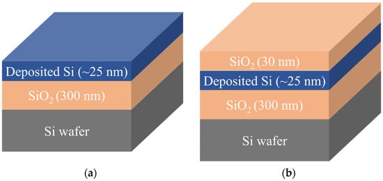
The schematic structures of the fabricated samples are shown in Figure 1. A thermally oxidized 8-inch (100) Si wafer served as the substrate, onto which Si films were deposited using a custom-built co-sputtering system and LPCVD (E1200, CENTROTHERM, Blaubeuren, Germany) to form PO structures on SiO2/Si stacks. To simulate encapsulation conditions typical of stacked devices, OPO structures were prepared by depositing a 30 nm thick SiO2 layer over the Si films using plasma-enhanced chemical vapor deposition (PECVD, FABStar+, TTL, Suwon-si, Republic of Korea). The detailed sputtering and LPCVD conditions for the poly-Si films are summarized in Table 1 and Table 2. The precise thicknesses of the deposited films and oxide layers were determined using spectroscopic ellipsometry (SE) and validated through cross-sectional TEM.
Figure 1.
Schematic of (a) PO and (b) OPO samples, each comprising ~25 nm-thick Si films on a thermally oxidized Si wafer. The OPO sample includes an additional SiO2 capping layer.
Table 1.
Sputtering condition for Si film.
Table 2.
LPCVD condition for Si film.
Furnace annealing was conducted in a custom-built tube furnace at 700 °C and 800 °C for 30 min at 1.6 Torr in a forming-gas ambient (4% H2 and 96% Ar) to evaluate the temperature-dependent crystallization of Si films. Both as-deposited and annealed samples were analyzed using spectroscopic ellipsometry (UVISEL, Horiba, Kyoto, Japan) and Raman spectroscopy (DXR3xi, Thermo Fisher Scientific, Waltham, MA, USA). SE measurements were conducted over a photon energy range of 1.5–5 eV at an incident angle of 70°, while Raman spectra were acquired using a 532 nm laser, covering a spectral range of 50–1800 cm−1. Surface roughness and morphological variations under different deposition and annealing conditions were assessed using atomic force microscopy (AFM, NX20, Park Systems, Gwacheon-si, Republic of Korea) in non-contact mode over a 1 × 1 μm2 scan area. The grain structures were examined using cross-sectional TEM (NEO ARM, JEOL Ltd., Tokyo, Japan).
2.2. Device Application and Electrical Characterization
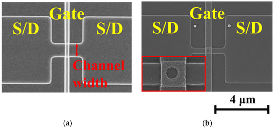
Based on the structural characterization results, transistors were fabricated using LPCVD-deposited films to investigate the electrical impact of the grain structure. A 300 nm SiO2 layer was thermally grown on an 8-inch Si wafer, followed by Si film deposition using LPCVD. The film then underwent extended annealing at 850 °C for 5 h to ensure sufficient crystallization. While this thermal budget is relatively high for conventional CMOS-under-Array integration, it is considered a highly feasible condition when adopting hybrid bonding technology [1]. This approach allows for the independent fabrication of peripheral CMOS and memory cell arrays on separate wafers, thereby effectively eliminating thermal constraints on the underlying logic circuits. Subsequently, channel regions were patterned using KrF lithography. Transistors with a channel width greater than 1 μm were defined using conventional single-step patterning (Figure 2a), while sub-100 nm channels were formed by etching holes to define the active regions (Figure 2b). Channel widths were confirmed using SEM (SU8010, Hitachi, Tokyo, Japan) for larger devices and TEM for sub-100 nm devices. The fabricated transistors included various channel widths, categorized into nanoscale and microscale dimensions. To ensure statistical reliability, five representative devices were systematically characterized for each respective channel width. Transistors were fabricated by thermally growing ~11 nm-thick gate oxides, followed by gate patterning and As implantation to define the source and drain (S/D) regions. The grain size in the channel regions was analyzed using crystal orientation mapping via ASTAR analysis (Tecnai, FEI, Hillsboro, OR, USA). To ensure statistical reliability, the average grain size was determined using the line intercept method, with measurements averaged over 20 distinct lines across the mapped region [14]. Id-Vg characteristics were measured using a parameter analyzer (4200A-SCS, Keithley, Cleveland, OH, USA) at Vd = 1 V over a gate voltage range of −3 V to 5 V, while Ioff was extracted from the measurements.
Figure 2.
Top-view SEM images of test transistors with varying channel widths: A transistor with a (a) channel width of 1 μm and (b) sub-100 nm channel width.
3. Results and Discussion
3.1. Selection of Deposition Method
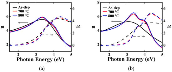
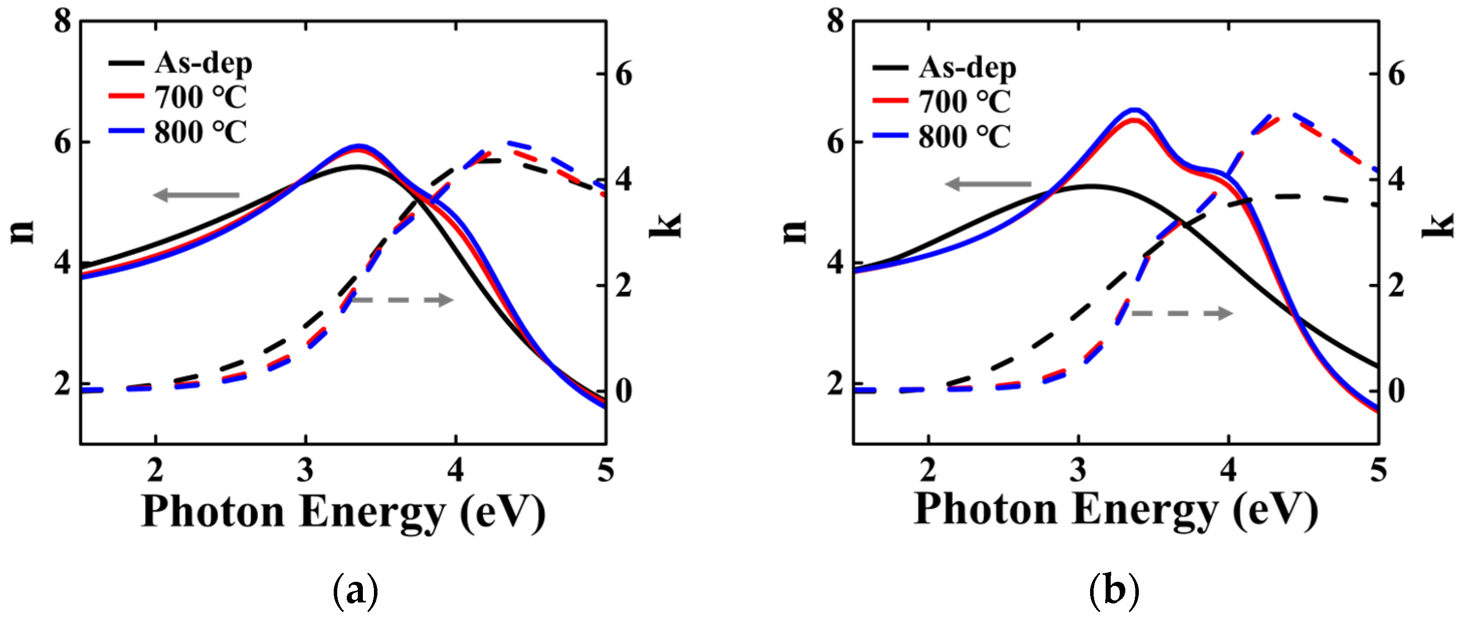
Figure 3 shows the SE spectra of the Si films with a PO structure deposited using sputtering and LPCVD. The refractive index (n) and extinction coefficient (k) for the as-deposited LPCVD Si films, which exhibit amorphous-like structures, were extracted using the Tauc-Lorentz (TL) model [15]. For all other samples, including the annealed LPCVD films and as-deposited annealed sputtered films, the Kato-Adachi (KA) function was applied, as their spectral features correspond with those of crystalline Si [16]. Upon annealing, the sputtered films exhibited minimal changes in spectral shape and peak positions, indicating minor structural changes. Conversely, the LPCVD films exhibited distinct spectral changes, with multiple n and k peaks characteristic of crystalline Si [17,18,19]. The increase after annealing indicated improved crystallinity in the LPCVD films, which exhibited higher peak intensities than the sputtered films [19].
Figure 3.
SE spectra of (a) sputtered and (b) LPCVD Si films for the PO structures. The solid and dashed lines represent the refractive index (n) and extinction coefficient (k), respectively. The black, red and blue colors correspond to the as-deposited (As-dep) and annealed samples at 700 °C and 800 °C, respectively.
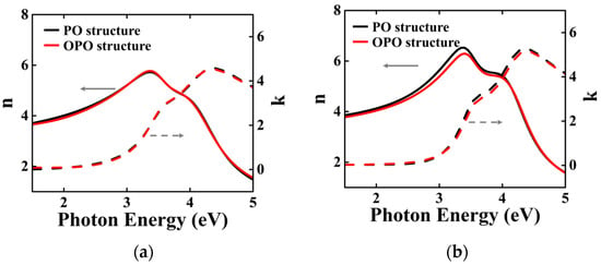
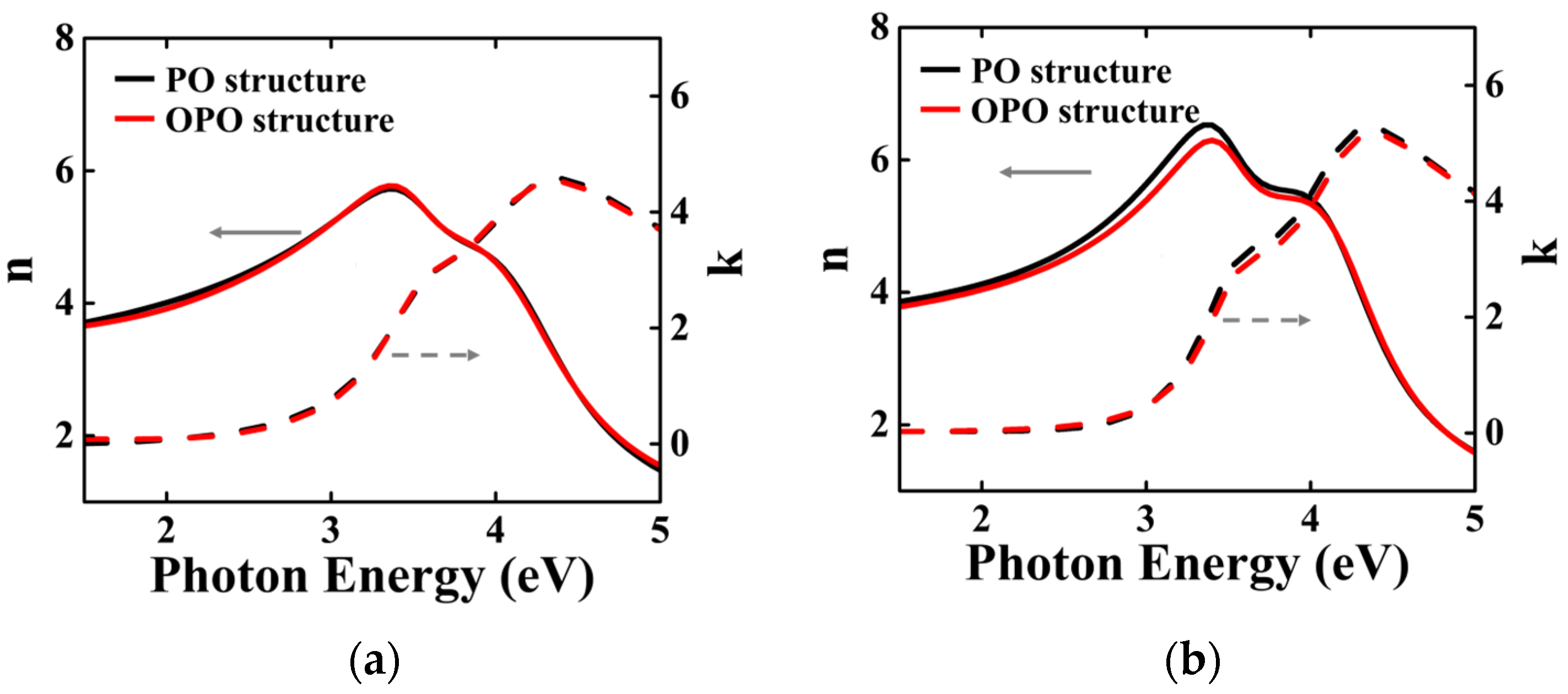
Figure 4 compares the SE spectra of sputtered and LPCVD Si films with PO and OPO structures after annealing at 800 °C. Both deposition methods exhibited characteristic poly-Si features, including distinct n and k peaks. A similar trend was observed for the sputtered Si in the OPO structure, indicating that sputtering inherently limits Si film crystallization regardless of structure. In contrast, the LPCVD samples maintained well-defined spectral features (Figure 4b) even under the OPO structure, with only minor reductions compared to the PO structure, indicating that crystallinity remained relatively high despite the oxide capping layer.
Figure 4.
SE spectra of (a) sputtered and (b) LPCVD Si films for the PO and OPO structures annealed at 800 °C. The solid and dashed lines represent n and k, respectively. The black and red colors correspond to the PO and OPO structures, respectively.
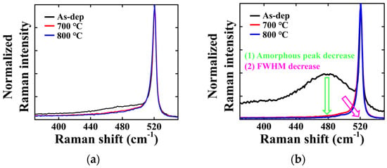
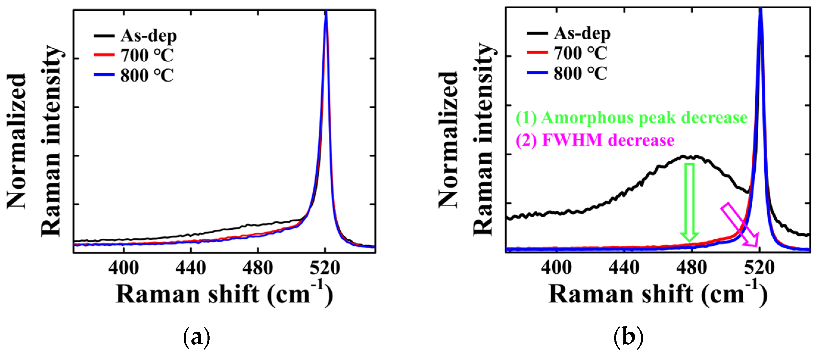
Figure 5 shows the normalized Raman spectra of the PO-structured Si films deposited via sputtering and LPCVD before and after annealing. The sputtered samples exhibited a peak at 480 cm−1 even after annealing, indicating incomplete crystallization. Contrarily, the as-deposited LPCVD films exhibited a broad peak near 480 cm−1. Upon annealing, a distinct peak appeared at 520.3 cm−1, which corresponds with crystallization [20].
Figure 5.
Normalized Raman spectra of the PO-structured Si films deposited via (a) sputtering and (b) LPCVD, shown in the as-dep state and after annealing at 700 °C and 800 °C.
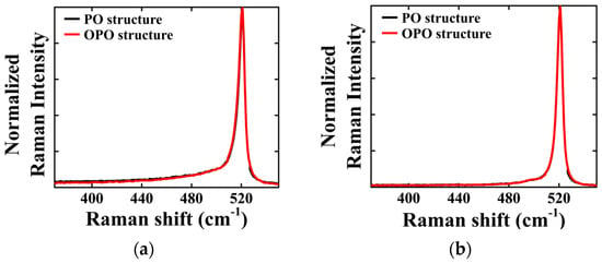
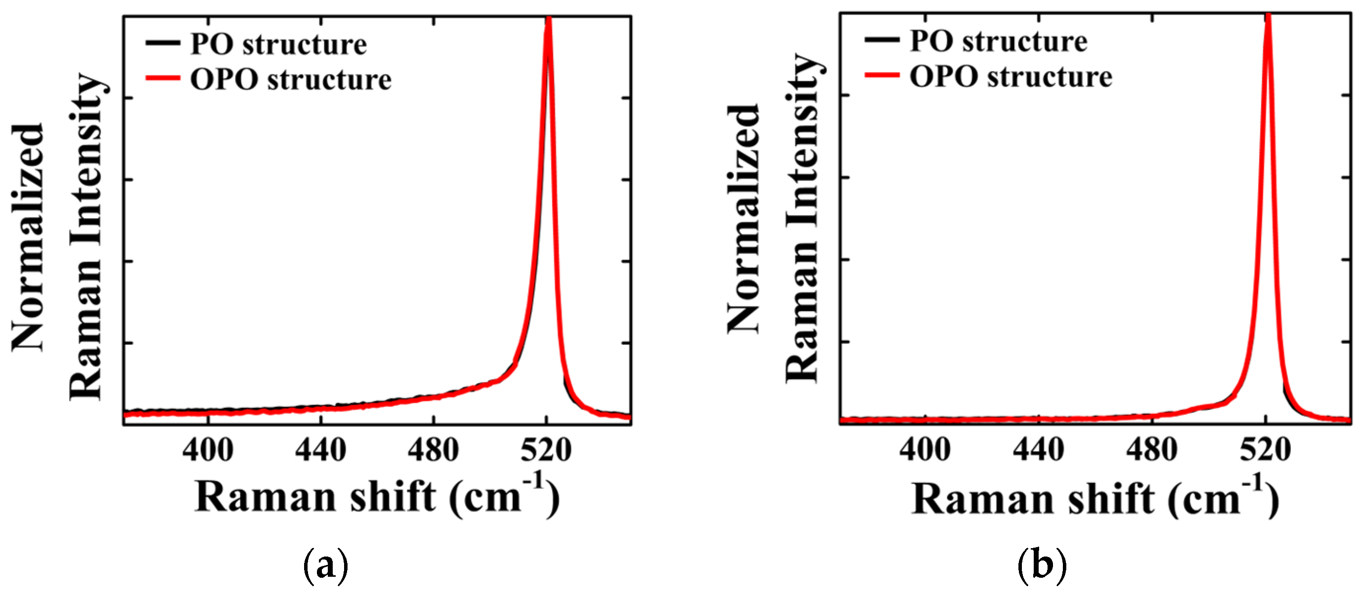
Figure 6 compares the Raman spectra of the PO and OPO structures after annealing at 800 °C. In the sputtered and LPCVD films, the OPO structures exhibited a minor change at 520.3 cm−1, indicating that the oxide capping layer had minimal effect on crystallization [20].
Figure 6.
Normalized Raman spectra of PO and OPO structures for Si films deposited via (a) sputtering and (b) LPCVD after annealing at 800 °C.
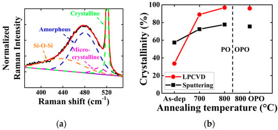
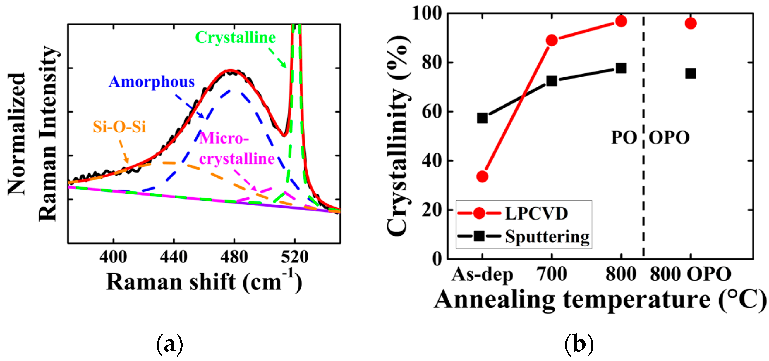
To quantitatively evaluate crystallinity, the Raman spectra were deconvoluted over the 370–550 cm−1 range using fixed peak positions at 480 and 520.3 cm−1, with an additional component included to account for microcrystalline features (Figure 7a). A peak at approximately 440 cm−1 was attributed to Si-O-Si bending vibrations [21]. Crystallinity was calculated using the weighted peak area method [22] as follows:
where , , and represent the areas of the crystalline, microcrystalline, and amorphous peaks, respectively. The corresponding values are shown in Figure 7b.
Figure 7.
(a) Raman spectrum of as-deposited LPCVD Si of PO structure with peak deconvolution, where the black and red lines represent the experimental Raman spectrum and the sum of deconvoluted peaks, respectively. (b) Crystallinity of Si films deposited via sputtering and LPCVD calculated using Raman deconvolution analysis, where the black and red symbols indicate the sputtered and LPCVD Si films, in that order.
The sputtered samples exhibited a slight increase in crystallinity, from approximately 57% to 78%, thereby indicating limited grain growth even after annealing. Contrarily, the crystallinity of the LPCVD samples increased considerably, from approximately 34% in the as-deposited state to 97% after annealing at 800 °C, remaining nearly unchanged in the OPO structure. Sputtered Si films generally exhibit high internal stress and low adatom mobility, thereby suppressing grain boundary migration and hampering crystallization during annealing [23,24,25].
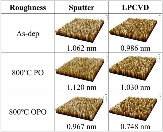
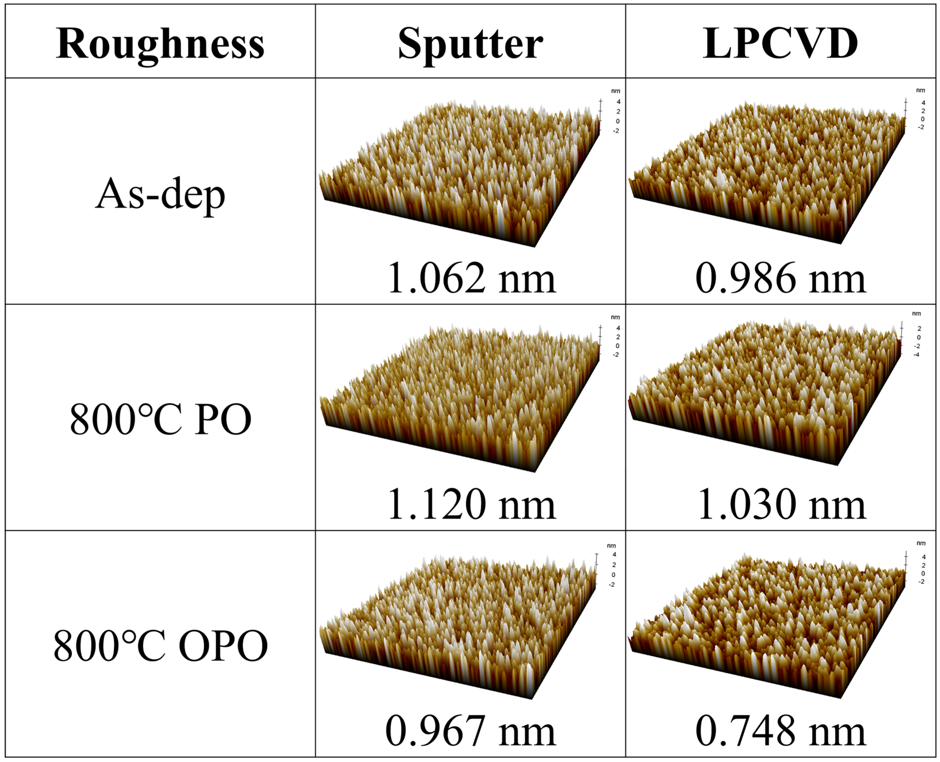
Changes in surface morphology were assessed by conducting AFM analysis over a 1 μm × 1 μm area (Figure 8). The measured RMS roughness is approximately 1 nm, which is a typical value for poly-Si films and is consistent with previous reports [26,27]. A slight increase in roughness was observed after annealing with the PO structure and a slight decrease with the OPO structure for both sputtered and LPCVD films. However, these changes were insignificant. Hence, annealing under either structure had minimal impact on the surface morphology.
Figure 8.
Surface roughness of Si films under different conditions: as-dep, annealed at 800 °C with PO and OPO structures.
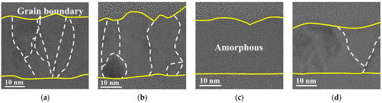
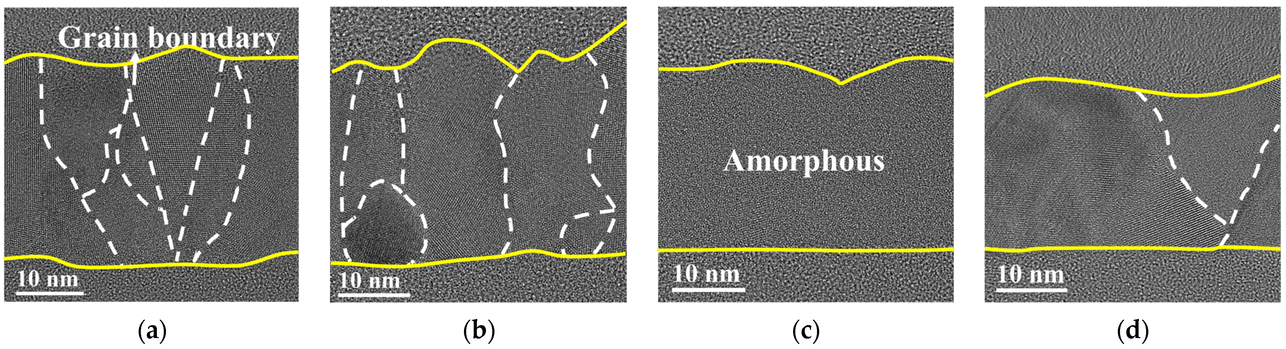
Cross-sectional TEM analyses were conducted on Si films deposited via sputtering and LPCVD to investigate grain formation from a vertical perspective. After annealing at 800 °C, both films exhibited vertically oriented grains, indicating columnar growth. In sputtered films, horizontally aligned grain boundaries were observed within the vertically oriented grains (Figure 9a,b), indicating incomplete columnar formation. These boundaries, parallel to the substrate, may serve as continuous leakage paths along the channel direction, thereby increasing Ioff [28]. Conversely, the LPCVD films initially exhibited an amorphous phase (Figure 9c). After annealing, the grain growth resulted in larger grains with a well-defined columnar structure spanning the entire film thickness, even in sub-30 nm layers (Figure 9d). This columnar-shaped structure is expected to suppress grain boundary-related leakage paths, thereby improving electrical stability [29,30].
Figure 9.
Cross-sectional TEM images of Si films: (a) As-deposited sputtered film, (b) sputtered film annealed at 800 °C, (c) as-deposited LPCVD film, (d) LPCVD film annealed at 800 °C. The yellow solid line and white dashed line indicate the Si/SiO2 interfaces and grain boundaries, respectively.
3.2. Device Application and Electrical Characterization
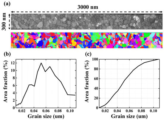
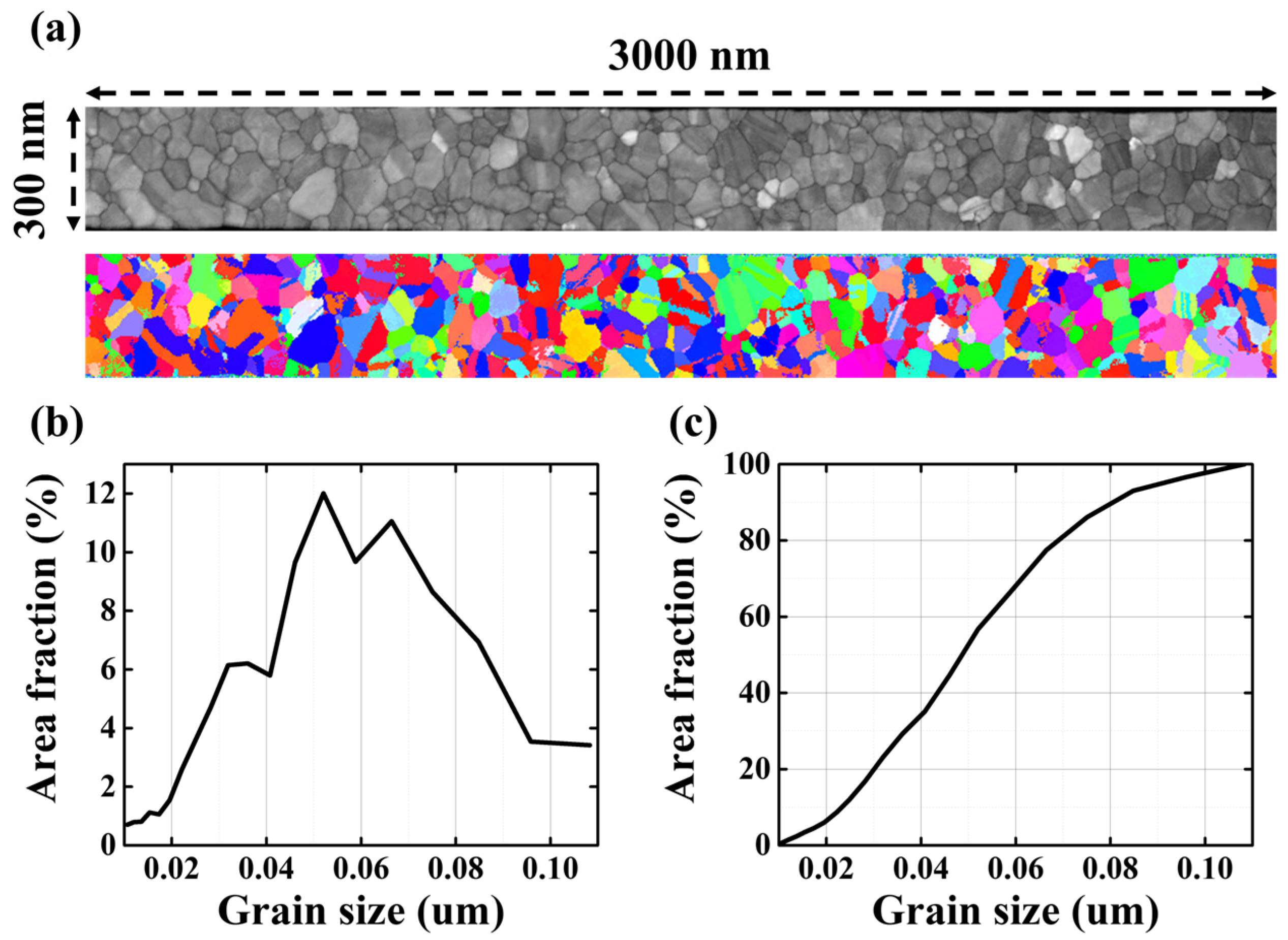
Based on the aforementioned results, further analysis was conducted on LPCVD samples, including ASTAR orientation mapping after extended annealing at 850 °C for 5 h. ASTAR was conducted on poly-Si films under similar annealing conditions as in device fabrication to examine the grain size within transistor channels. Figure 10a shows a plan-view TEM image and the corresponding ASTAR grain orientation map of the LPCVD film. Figure 10b,c show the grain size distribution and cumulative plot from the mapped region. The average grain size was approximately 50 nm, with grains < 20 nm accounting for less than 10%. This indicates that annealing enables grain coarsening while limiting the formation of small, defect-prone grains.
Figure 10.
(a) Plan-view TEM image and ASTAR orientation map of LPCVD poly-Si annealed at 850 °C, where different colors represent individual grains. (b) grain size distribution; (c) cumulative grain size plot.
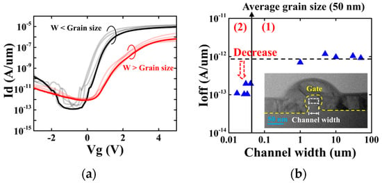
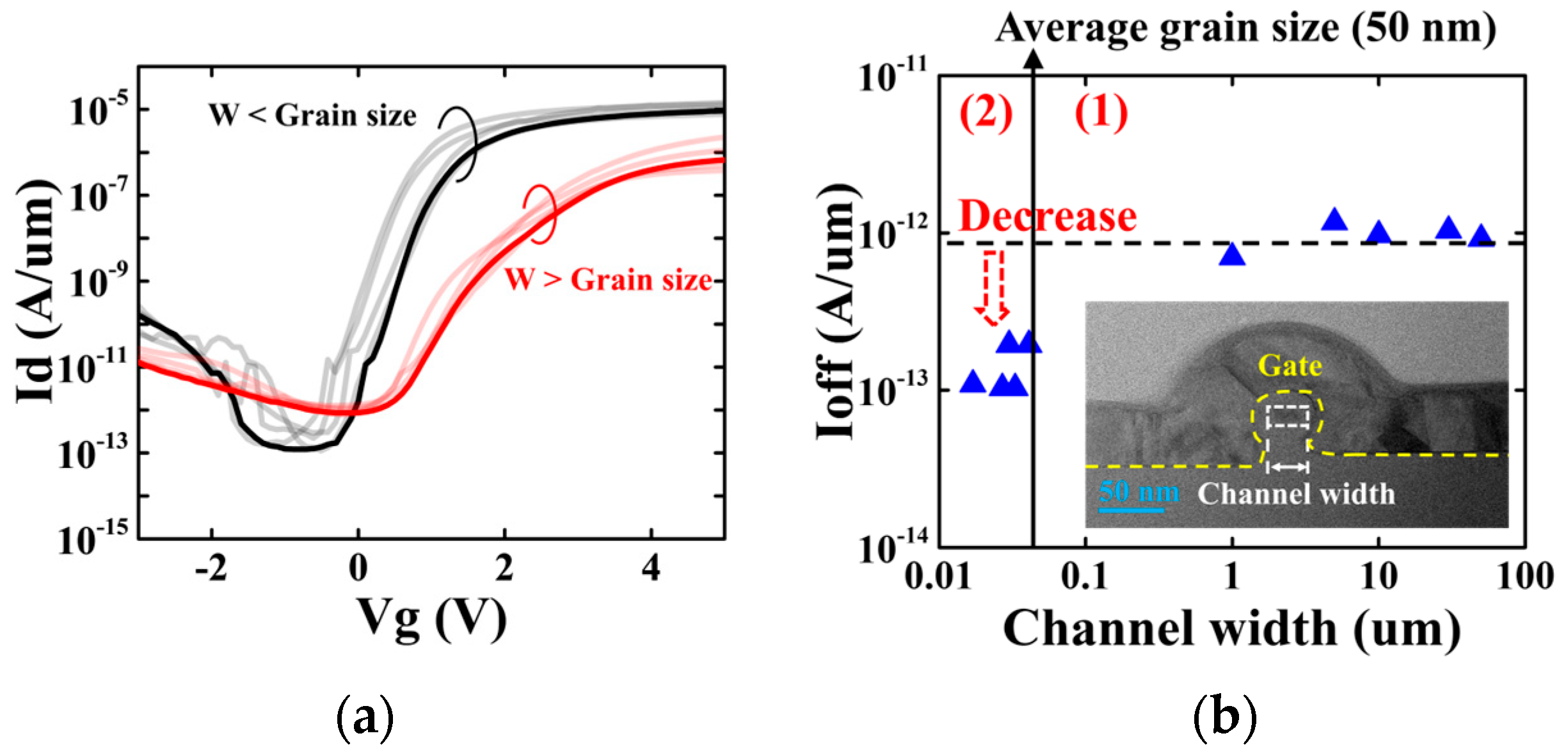
The effect of structural features on electrical performance was examined by fabricating transistor test structures using LPCVD poly-Si films annealed under similar conditions as those used in the ASTAR analysis. Figure 11a shows the Id-Vg characteristics of transistors with channel widths of 0.02 and 10 μm, measured at 75 °C. Normalized Ioff values were extracted from Id-Vg curves for different channel widths at 75 °C (Figure 11b). The 0.02 μm channel exhibited a higher normalized Ion and lower SS than the 10 μm channel. This behavior is attributed to the limited grain boundaries in the 0.02 μm channel, which is narrower than the average grain size. The lateral restriction in this narrow channel effectively minimizes the probability of grain boundaries aligning along the conduction path, which contributes to the enhanced Ion and SS by minimizing carrier scattering and interface trapping-both of which degrade device performance [31]. In contrast to sc-Si, which exhibits nearly constant Ioff across different channel widths [32,33], the poly-Si channel in Figure 11b shows a channel-width-dependent Ioff.
Figure 11.
(a) Id-Vg characteristics and (b) Normalized Ioff of poly-Si channel transistor as a function of the channel width. The regions labeled (1) and (2) correspond to the channel width smaller and larger than the grain size, respectively.
Two representative regions are highlighted in Figure 11b: (1) transistors with channel widths exceeding the average grain size; (2) transistors with narrower channels. In region 1, the channel comprises numerous grains, thereby increasing the probability of carriers encountering grain boundaries along the current path. Consequently, it virtually ensures the formation of continuous longitudinal grain boundaries aligned with the current flow, which act as preferential leakage paths resulting in a high Ioff [33,34]. In region 2, as channel width scales down to become smaller than the average grain size, the lateral space is restricted. Consequently, the statistical probability of a grain boundary continuously extending along the current flow without interruption is significantly suppressed. This geometric restriction effectively limits the formation of continuous longitudinal leakage channels, contributing to a reduced Ioff. This result implies that not only the number, but also the orientation of the grain boundaries relative to the current direction can affect the leakage channels, minimizing the probability of boundary-aligned leakage paths. Crucially, this structural advantage translates into highly consistent electrical performance. Across the evaluated transistors in region 2, where the channel width is narrower than the average grain size, key parameters including Ion and Vth exhibited highly uniform distributions with negligible device-to-device variability. Furthermore, all 5 evaluated devices in this regime consistently demonstrated a significant reduction in the normalized Ioff, confirming that this leakage suppression is a statistically reliable and reproducible phenomenon.
The aforementioned results highlight the importance of grain boundary engineering―including the grain size, structure, and size distribution―for enhancing transistor performance. Although Figure 10c shows a minor proportion of sub-20 nm grains, the remarkable electrical uniformity observed in the evaluated nanoscale devices suggests that the severe lateral geometric restriction mitigates their local impact. To satisfy the demanding technologies, further process optimization is required to effectively suppress the leakage pathways associated with boundary-aligned conditions.
4. Conclusions
In this study, the crystallization behavior and microstructural characteristics of Si films deposited via sputtering and LPCVD under PO and OPO structures were investigated to assess their influence on the grain structure and electrical performance of poly-Si channels for stacked memory applications. Structural analyses using SE, Raman spectroscopy, AFM, and TEM revealed that the LPCVD-deposited Si films exhibited superior crystallinity, larger grain sizes, and smoother surfaces than those deposited using sputtering. The SiO2 capping layer had a minimal impact on the Si crystallization. Additionally, the LPCVD-deposited poly-Si exhibits a well-defined columnar structure.
Driven by this structural superiority, transistor-level electrical characterizations and width-dependent Ioff analyses were exclusively performed on the LPCVD-based devices. ASTAR orientation mapping and transistor-level electrical measurements suggest that this structural enhancement improved transistor performance. When the average grain size exceeds the channel width, normalized Ioff improves, indicating that reducing the channel width below the average grain size is crucial for suppressing leakage and improving transistor performance in poly-Si channels with columnar grain, particularly in stacked-memory applications. These findings suggest that future grain engineering and process development must simultaneously address improved crystallinity, grain boundary alignment, and annealing optimization to achieve consistent device performance in scaled memory systems. Based on these results, LPCVD-deposited poly-Si subjected to optimized annealing offers a structurally and electrically viable channel material for 3D memory applications. Meanwhile, the oxide capping layer serves as a highly compatible encapsulation scheme, and together they provide a strong foundation for future integration and scaling.
Author Contributions
Conceptualization, S.J.K., W.S. and Y.W.P.; methodology, S.J.K., J.H.P. and H.Y.J.; validation, S.J.K., W.S. and Y.W.P.; investigation, S.J.K., J.H.P. and H.Y.J.; Formal analysis, S.J.K., I.-S.P., T.L., W.S., Y.G., K.L., D.H., Y.W.P. and J.A.; writing—original draft preparation, S.J.K.; writing—review and editing, I.-S.P., T.L., W.S., Y.W.P. and J.A.; supervision, Y.W.P. and J.A.; project administration, Y.G., K.L., D.H., Y.W.P. and J.A.; funding acquisition, Y.G., K.L., D.H., Y.W.P. and J.A. All authors have read and agreed to the published version of the manuscript.
Funding
This work was supported by the Technology Innovation Program (or Industrial Strategic Technology Development Program) (“RS-2023-00235609”, Proposal of 3D DRAM development direction from the process development of vertical stacked cell transistors) funded By the Ministry of Trade, Industry & Energy (MOTIE, Republic of Korea) (1415187471)”, Samsung Electronics Co., Ltd. (IO241017-11002-01), the National Research Foundation of Korea (NRF) grant funded by the Korean government (Ministry of Science and ICT) (No. RS-2023-00260527).
Data Availability Statement
The datasets generated and/or analyzed during the current study are available from the corresponding authors upon request.
Conflicts of Interest
Youngin Goh, Kyunghwan Lee and Daewon Ha were employed by the Samsung Electronics Company. The remaining authors declare that the research was conducted in the absence of any commercial or financial relationships that could be construed as a potential conflict of interest.
Abbreviations
The following abbreviations are used in this manuscript:
| Poly-Si | Polycrystalline silicon |
| 3D | Three-dimensional |
| Ioff | Off-state current |
| LPCVD | Low-pressure chemical vapor deposition |
| TEM | Transmission electron microscopy |
| Sc-Si | Single-crystal silicon |
| DRAM | Dynamic random-access memory |
| Ion | On-state current |
| SS | Subthreshold swing |
| PO | Uncapped |
| OPO | Oxide-capped |
| PECVD | Plasma-enhanced chemical vapor deposition |
| SE | Spectroscopic ellipsometry |
| S/D | Source and drain |
| TL | Tauc-Lorentz |
| KA | Kato-Adachi |
| ASTAR | Automated crystal orientation and phase mapping |
References
- Choi, K.; Kim, S.; Seo, J.; Kang, H.; Chu, S.; Bae, S.; Kwon, J.; Kim, G.; Park, Y.; Kwak, J. A three dimensional DRAM (3D DRAM) technology for the next decades. In Proceedings of the 2024 IEEE Symposium on VLSI Technology and Circuits (VLSI Technology and Circuits), Honolulu, HI, USA, 16–20 June 2024; pp. 1–2. [Google Scholar]
- Chen, W.-C.; Lue, H.-T.; Wu, M.-H.; Lin, Y.-T.; Wang, K.-C.; Lu, C.-Y. A highly pitch-scalable capacitor-less 3D DRAM using cross-bar selection with gate-controlled thyristor (GCT) featuring high endurance and free read-disturb. In Proceedings of the 2023 International Electron Devices Meeting (IEDM), San Francisco, CA, USA, 9–13 December 2023; pp. 1–4. [Google Scholar]
- Yoo, M.; Lee, S.; Son, A.; Choi, S.; Kim, C.; Jang, K.; Choi, K.; Kim, Y.; Jeon, W.; Kim, S. DRAM Technology & Design Optimization for Sub-10nm and Beyond. In Proceedings of the 2024 IEEE International Electron Devices Meeting (IEDM), San Francisco, CA, USA, 7–11 December 2024; pp. 1–4. [Google Scholar]
- Pavlidis, V.F.; Savidis, I.; Friedman, E.G. Three-Dimensional Integrated Circuit Design; Newnes: London, UK, 2017. [Google Scholar]
- Im, J.S.; Sposili, R.S.; Crowder, M. Single-crystal Si films for thin-film transistor devices. Appl. Phys. Lett. 1997, 70, 3434–3436. [Google Scholar]
- Ohmura, Y.; Matsushita, Y.; Kashiwagi, M. Solid-phase lateral epitaxial growth onto adjacent SiO2 film from amorphous silicon deposited on single-crystal silicon substrate. Jpn. J. Appl. Phys. 1982, 21, L152. [Google Scholar]
- Brotherton, S. Polycrystalline silicon thin film transistors. Semicond. Sci. Technol. 1995, 10, 721. [Google Scholar] [CrossRef] [Scilit]
- Liu, P.-C.; Su, C.-J.; Li, P.-W.; Lin, H.-C. Monolithically integrated polysilicon/oxide-semiconductor hybrid thin-film transistors for advanced sensing. IEEE J. Electron Devices Soc. 2023, 11, 490–496. [Google Scholar]
- Lee, C.-K.; Chang, H.-L.; Chen, K.-M.; Huang, G.-W.; Kuo, C.-N.; Li, P.-W.; Lin, H.-C. Polycrystalline-Silicon CMOS Thin-Film Transistors With T-Shaped Gate and Lightly Doped Drain. IEEE Trans. Electron Devices 2024, 71, 5414–5420. [Google Scholar]
- Sugiura, N.; Chuang, C.-T.; Hsieh, C.-T.; Wu, C.-T.; Tsai, C.-Y.; Lin, C.-H.; Liu, C.-C.; Liu, C.-Y.; Yeh, C.-N.; Liu, C.-Y. 32-3: Invited Paper: 12.1-inch 169-ppi Full-Color Micro-LED Display Using LTPS-TFT Backplane. Proc. SID Symp. Dig. Tech. Pap. 2019, 50, 450–453. [Google Scholar]
- Park, J.; Jeong, H.; Park, E.; Park, G.; Ahn, C.-h.; Lee, S.; Won, J.; Kwon, H.-J.; Yu, H.-Y. High-Performance Monolithic 3D CMOS Enabled by Orientation-Aligned Seedless Laser Crystallization and Ultra-Shallow Laser Activation. In Proceedings of the 2025 Symposium on VLSI Technology and Circuits (VLSI Technology and Circuits), Kyoto, Japan, 8–12 June 2025; pp. 1–3. [Google Scholar]
- Jang, D.; Lee, J.; Park, C.; Ban, H.; Park, T. Laser annealing technology for storage node contact in 10 nm class DRAM. Jpn. J. Appl. Phys. 2026, 65, 02SP01. [Google Scholar] [CrossRef] [Scilit]
- Shin, H.; Yoon, D.; Jo, C.; Lee, K.; Oh, H.; Ko, D.-H. Characteristics of Si channel layer formed through recrystallization using nanosecond laser annealing for monolithic 3D integration. Mater. Sci. Semicond. Process. 2026, 202, 110121. [Google Scholar]
- Thorvaldsen, A. The intercept method—2. Determination of spatial grain size. Acta Mater. 1997, 45, 595–600. [Google Scholar] [CrossRef] [Scilit]
- Fried, M.; Lohner, T.; Aarnink, W.; Hanekamp, L.; Van Silfhout, A. Determination of complex dielectric functions of ion implanted and implanted-annealed amorphous silicon by spectroscopic ellipsometry. J. Appl. Phys. 1992, 71, 5260–5262. [Google Scholar] [CrossRef] [Scilit]
- Jellison, G., Jr.; Modine, F. Parameterization of the optical functions of amorphous materials in the interband region. Appl. Phys. Lett. 1996, 69, 371–373. [Google Scholar] [CrossRef] [Scilit]
- Petrik, P. Characterization of nanocrystals using spectroscopic ellipsometry. In Nanotechnology and Nanomaterials: Nanocrystals Synthesis, Characterization and Applications; InTechOpen: London, UK, 2012; pp. 29–40. [Google Scholar]
- Adachi, S.; Mori, H. Optical properties of fully amorphous silicon. Phys. Rev. B 2000, 62, 10158. [Google Scholar] [CrossRef] [Scilit]
- Pyo, J.; Lee, B.; Ryu, H.-Y. Evaluation of crystalline volume fraction of laser-annealed polysilicon thin films using raman spectroscopy and spectroscopic ellipsometry. Micromachines 2021, 12, 999. [Google Scholar] [CrossRef] [Scilit] [PubMed]
- Ganesan, J.P.; Iqbal, N.; Krsmanovic, M.; Torres-Davila, F.; Dickerson, A.; Davis, K.O.; Tetard, L.; Banerjee, P. Raman Microspectroscopy of a Multi-Crystalline Silicon Solar Cell. IEEE J. Photovolt. 2021, 12, 230–237. [Google Scholar] [CrossRef] [Scilit]
- Vaccaro, G.; Agnello, S.; Buscarino, G.; Gelardi, F. Thermally induced structural modification of silica nanoparticles investigated by Raman and infrared absorption spectroscopies. J. Phys. Chem. C 2010, 114, 13991–13997. [Google Scholar] [CrossRef] [Scilit]
- Smit, C.; Van Swaaij, R.; Donker, H.; Petit, A.; Kessels, W.; Van de Sanden, M. Determining the material structure of microcrystalline silicon from Raman spectra. J. Appl. Phys. 2003, 94, 3582–3588. [Google Scholar] [CrossRef] [Scilit]
- Chen, Z.; Liu, F.; Yang, W.; Wang, H.; Yang, G.; Zhou, Y. Influence of grain boundary energy on the grain size evolution in nanocrystalline materials. J. Alloys Compd. 2009, 475, 893–897. [Google Scholar] [CrossRef] [Scilit]
- Abadias, G.; Chason, E.; Keckes, J.; Sebastiani, M.; Thompson, G.; Barthel, E.; Doll, G.; Murray, C.; Stoessel, C.; Martinu, L. Review Article: Stress in Thin Film s and Coatings: Current Status. Chall. Prospect. 2018, 36, 020801. [Google Scholar]
- Maeda, K.; Umezu, I. Defect formation mechanism during plasma enhanced chemical vapor deposition of undoped a-Si: H. J. Non-Cryst. Solids 1998, 227, 43–47. [Google Scholar]
- Jeong, J.-K.; Sung, J.-Y.; Ko, W.-S.; Nam, K.-R.; Lee, H.-D.; Lee, G.-W. Physical and electrical analysis of poly-Si channel effect on SONOS flash memory. Micromachines 2021, 12, 1401. [Google Scholar] [CrossRef] [Scilit] [PubMed]
- Choi, M.; Lee, S.; Kang, S.; Jang, S.; Siddik, A.B.; Jang, J. High temperature solid phase crystallization of a-Si on glass by short time blue laser exposure for display backplane. IEEE Electron Device Lett. 2022, 43, 1890–1893. [Google Scholar] [CrossRef] [Scilit]
- Wang, B.; Gao, B.; Wu, H.; Qian, H. A drain leakage phenomenon in poly silicon channel 3D NAND flash caused by conductive paths along grain boundaries. Microelectron. Eng. 2018, 192, 66–69. [Google Scholar] [CrossRef] [Scilit]
- Levinson, J.; Shepherd, F.; Scanlon, P.; Westwood, W.; Este, G.; Rider, M. Conductivity behavior in polycrystalline semiconductor thin film transistors. J. Appl. Phys. 1982, 53, 1193–1202. [Google Scholar] [CrossRef] [Scilit]
- Seto, J.Y. The electrical properties of polycrystalline silicon films. J. Appl. Phys. 1975, 46, 5247–5254. [Google Scholar] [CrossRef] [Scilit]
- Yamaguchi, K. Modeling and characterization of polycrystalline-silicon thin-film transistors with a channel-length comparable to a grain size. J. Appl. Phys. 2001, 89, 590–595. [Google Scholar]
- Hilbert, B.; Pavanello, M. Electrical characterization of mosfets from a 180 nm cmos technology. In Proceedings of the 20th Microelectronics Student Forum, São Paulo, Brazil, 26–28 August 2020. [Google Scholar]
- Hogyoku, M.; Izumida, T.; Tanimoto, H.; Aoki, N.; Onoue, S. Grain-boundary-limited carrier mobility in polycrystalline silicon with negative temperature dependence: Modeling carrier conduction through grain-boundary traps based on trap-assisted tunneling. Jpn. J. Appl. Phys. 2019, 58, SBBA01. [Google Scholar]
- Bersuker, G.; Yum, J.; Vandelli, L.; Padovani, A.; Larcher, L.; Iglesias, V.; Porti, M.; Nafría, M.; McKenna, K.; Shluger, A. Grain boundary-driven leakage path formation in HfO2 dielectrics. Solid-State Electron. 2011, 65, 146–150. [Google Scholar]

Disclaimer/Publisher’s Note: The statements, opinions and data contained in all publications are solely those of the individual author(s) and contributor(s) and not of MDPI and/or the editor(s). MDPI and/or the editor(s) disclaim responsibility for any injury to people or property resulting from any ideas, methods, instructions or products referred to in the content. |
© 2026 by the authors. Licensee MDPI, Basel, Switzerland. This article is an open access article distributed under the terms and conditions of the Creative Commons Attribution (CC BY) license.