


Abstract
Single crystals of different V(Sn, Sb)2 phases were grown via the self-flux method by employing an excess of Sn and Sb. The obtained crystals were studied using X-ray diffraction and EDX spectroscopy, which revealed the existence of two new ternary phases and two solid solutions based on the binary VSn2 to VSb2 phases, showing peculiar multi-step structural evolution upon going from the VSn2 side to the VSb2 side of the system. The first novel phase τ1 crystallizes in the monoclinic unit cell, while the second phase—τ2—adopts an orthorhombic crystal structure. The discovered phases derive their structure from the parent phases VSn2 and VSb2 and are built from linear chains of fused V(Sn, Sb)8 antiprisms. These chains are then coupled into layers, which are stacked either right on top of each other or with a 60° twist. The twists are supported by Sn atoms located at a boundary between the layers. Thus, upon going from VSn2 to VSb2, the number of twists per layer decreases from one in VSn2 to 2/3 in τ1, and to 1/2 in τ2, ultimately ending at zero in VSb2. While the Sn atoms have a larger radius compared to that of Sb, the volume per one atom decreases in the VSnx′Sb2−x′ solid solution with increasing Sn content before returning to the expected increase in the τ1-τ2-VSn2−xSbx sequence. The decrease in volume in the former is caused by the decrease in V-V distances inside the chains, which is caused by the change in character of the V-E interactions, where Sb atoms form two-center V-Sb bonds, while Sn atoms act as bridges forming three-center V-Sn-V bonds, as revealed by our DFT calculations.
1. Introduction
Valence electron concentration (or VEC) is one of the most important general criteria which defines the structure and properties of T-E intermetallics formed by transition (T) and main group (E) metals [1,2]. It is defined as the total number of valence electrons divided by the number of T atoms [1].
Heterovalent substitution using atoms of the same row of the periodic table can continuously change the VEC without large changes to the unit cell volume, allowing one to induce metal-insulator transitions [3] or to change the type of magnetic order [4].
While the heavily delocalized nature of chemical bonding in intermetallics may suggest an even distribution of dopant atoms and that the effects of such a substitution can be accounted for by band theory, our recent investigations show that local electronic factors are just as important, if not more [5,6,7].
To examine the impact of heterovalent doping further, we have chosen the V-Sn-Sb ternary system, which was surprisingly poorly investigated. In particular, we have focused on the pseudo-binary section based on two related compounds—VSb2 and VSn2. Despite not being formally isostructural, VSb2 and VSn2 belong to two related structure types—CuAl2 and CuMg2, respectively—and share common basic structure blocks in the form of flat layers of fused VE8 antiprisms [8,9].
In the previous studies found in the literature, the structural stability of CuAl2 and CuMg2 was investigated primarily by doping the transition-element substructure, where it was observed that the former structure type favors higher VEC (>14.75 e−/T), while the latter prefers lower VEC (<14 e−/T), with another similar structure type—NiMg2—found in between those VEC regions [10,11,12,13,14,15].
In our work, we have investigated structural evolution between VSb2 and VSn2 and observed that both VSb2 and VSn2 form extended solutions, and the transformation between these phases involves the formation of two intermediate ternary phases τ1 and τ2, which are related to the binary compounds, but crystallize in their own structure types. In the present paper, we report on their synthesis, crystal growth, homogeneity ranges, and crystal and electronic structures. We compare the structural features between the phases and discuss the possible causes behind the structural changes.
2. Materials and Methods
Single crystals of the V(Sn, Sb)2 phases were grown from the elements. High-purity V chips (99.95%, Merck, Darmstadt, Germany), Sb (99.99%, Sigma-Aldrich, Steinheim, Germany), and Sn ingots (99.999%, Sigma-Aldrich, Steinheim, Germany) were used as received. The excess of Sn and Sb was used as a flux. The starting element ratios were either V(Sn, Sb)5 or V(Sn, Sb)10. A detailed summary of the samples, their initial compositions, and the results of the phase and elemental analysis are given in Table S1 in the Supporting Information. It is worth noting that the Sb/Sn ratio in the obtained single crystal differs from that in the initial mixture, and the Sb concentration in the crystals is always higher than the Sb concentration in the initial mixture.
In order to prevent oxidation of the samples, they were placed in evacuated and sealed silica tubes prior to annealing. The annealing was performed using the following temperature profile. Initially, the samples were heated up to 1000 °C, held at this temperature for 24 h, and then slowly cooled down to 700 °C at a rate of 5 °C/h and held at this temperature for a week. The samples were then quenched in water. The majority of the flux was removed in a centrifuge at 700 °C, while the rest was removed mechanically. As a result of the synthesis, several small plate- or rod-shaped silvery crystals (up to 1 mm in length) were obtained (Figure S1 in the Supporting Information).
Alongside ternary phases and solid solutions, single crystals of pure binary phases VSn2 and VSb2 were also prepared. VSn2 was prepared by a technique identical to the one used for the ternary phases. The technique for the VSb2 single crystals was slightly different. In particular, the crystals were cleaned from the residual Sb flux in the temperature gradient in the evacuated tube using high Sb volatility. One side of the sealed silica tube was placed in the furnace and heated up to 600 °C, while the other side was kept at room temperature outside the furnace.
The elemental analysis of the obtained crystals was performed by energy dispersion X-ray spectroscopy (Tokyo, Japan) using an electron microscope JSM JEOL 6490LV equipped with an Oxford Instruments Analytical INCA X-Sight system for the EDX analysis. The recorded spectra were analyzed using the INCA Microanalysis Suite (Abingdon, UK).
The crystal structure was studied via single crystal X-ray diffraction. The structural analysis was performed at 100 K on the crystals from the VSn10, VSn4.125Sb0.875, VSn3.625Sb1.375, VSn7.5Sb2.5, VSn7.5Sb2.5, VSn3.125Sb1.875, VSn2.75Sb2.25, VSn2.5Sb2.5, and VSb10 samples (Table S1 in Supporting Information) using a Bruker D8 QUEST diffractometer, Billerica, MA, USA (Mo Kα, λ = 0.71073 Å) equipped with a CMOS PHOTON II detector.
The crystal structure was solved by the Superflip program (Version 09/21/20) [16] implemented in the Jana2006 package (Version 15/02/2021) [16]. The latter was also used for crystal structure refinement. Since Sn and Sb atoms are very close in terms of their X-ray scattering factors, we could not distinguish them in our X-ray diffraction experiments. Although in an earlier report on a related compound, TiSnSb of the CuMg2 structure type, the authors did manage to resolve Sn and Sb sites [15], in our case we observed practically identical results between different ordered models.
Still, based on the obtained interatomic distances, it was evident that these atoms are not distributed equally within the structure of VSn2−xSbx, τ1 and τ2. Thus, the ratio of Sb and Sn at the sites was fixed at more realistic arbitrary values chosen in accordance with the atomic environments and total interatomic distances (see Supporting Information for more details). Given that it was reported that the VSb2 phase can exhibit V vacancies [8], we have attempted to refine the occupancies of the V sites. This yielded full occupancies within 3σ for all studied compounds.
The crystallographic information files are deposited in the CCDC (ref. numbers 2586483-2586490) and available as part of the Supporting Information. For the visualization of the crystallographic data, the VESTA 3 software was used [17].
The obtained crystals were also crushed and studied using powder X-ray diffraction (Rimsting, Germany) on a Huber G670 diffractometer (Cu Kα1, λ = 1.54056 Å). Since the samples contained noticeable amounts of additional phases, only le Bail fits were performed.
Electronic structure calculations for VSb2 and VSn2 were performed using density functional theory (DFT) in a tight-binding approximation in the TB-LMTO-ASA package (Version 4.7) [18], which was previously used in the literature for a similar analysis of VSb2 and its Ti-based analogue, TiSb2 [8]. The DFT calculations were performed using the Perdew-Wang 92 functional [19]. Reciprocal space integration was performed on a 16 × 16 × 16 k-point grid using the tetrahedron method [20]. The experimentally obtained unit cell parameters and atomic positions were used for calculations. The real-space analysis of crystal orbital Hamilton populations (COHPs) [21], electron density distribution, and electron localization function (ELF) calculations [22,23] were also performed in the TB-LMTO-ASA package.
Topological analysis of the electron density and ELF, including determination of critical points and basin boundaries, as well as electron density integration, was performed in accordance with Bader’s theory of atoms in molecules [24] using the Critic2 package (Version 1.2) [25,26]. The visualization of the obtained distribution maps was performed using the VESTA package (Version 3.5.7) [17].
3. Results and Discussion
3.1. Structural Transformations and Phase Equilibria on the VSn2-VSb2 Section
Our single crystal and powder X-ray diffraction data revealed a peculiar multistage transformation from VSn2 of the CuMg2 structure type to VSb2 of the CuMg2 type.
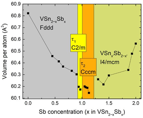
At low concentrations, Sb simply replaces Sn in VSn2, thus forming the VSn2−xSbx solid solution, which exists until x ~ 0.9. The structure then transforms from orthorhombic into a monoclinic one, τ1, which is unique to this system. The composition of the τ1 phase is close to VSnSb. This phase appears to have a very narrow homogeneity range and was observed in only two of the obtained samples. Our EDX measurements showed that Sn/Sb ratio can vary from 1.07/0.93 to 1.03/0.97. Upon increasing the Sb concentration, the structure reverts back to the orthorhombic crystal system; however, there is a different structure of τ2, which again has its own structure type. Similar to τ1, τ2 displays a narrow homogeneity range from VSn0.95Sb1.05 to VSn0.87Sb1.13. Upon further Sb doping, the structure ultimately settles into the VSb2-based solid solution VSnx’Sb2−x′ of the tetragonal CuMg2 type.
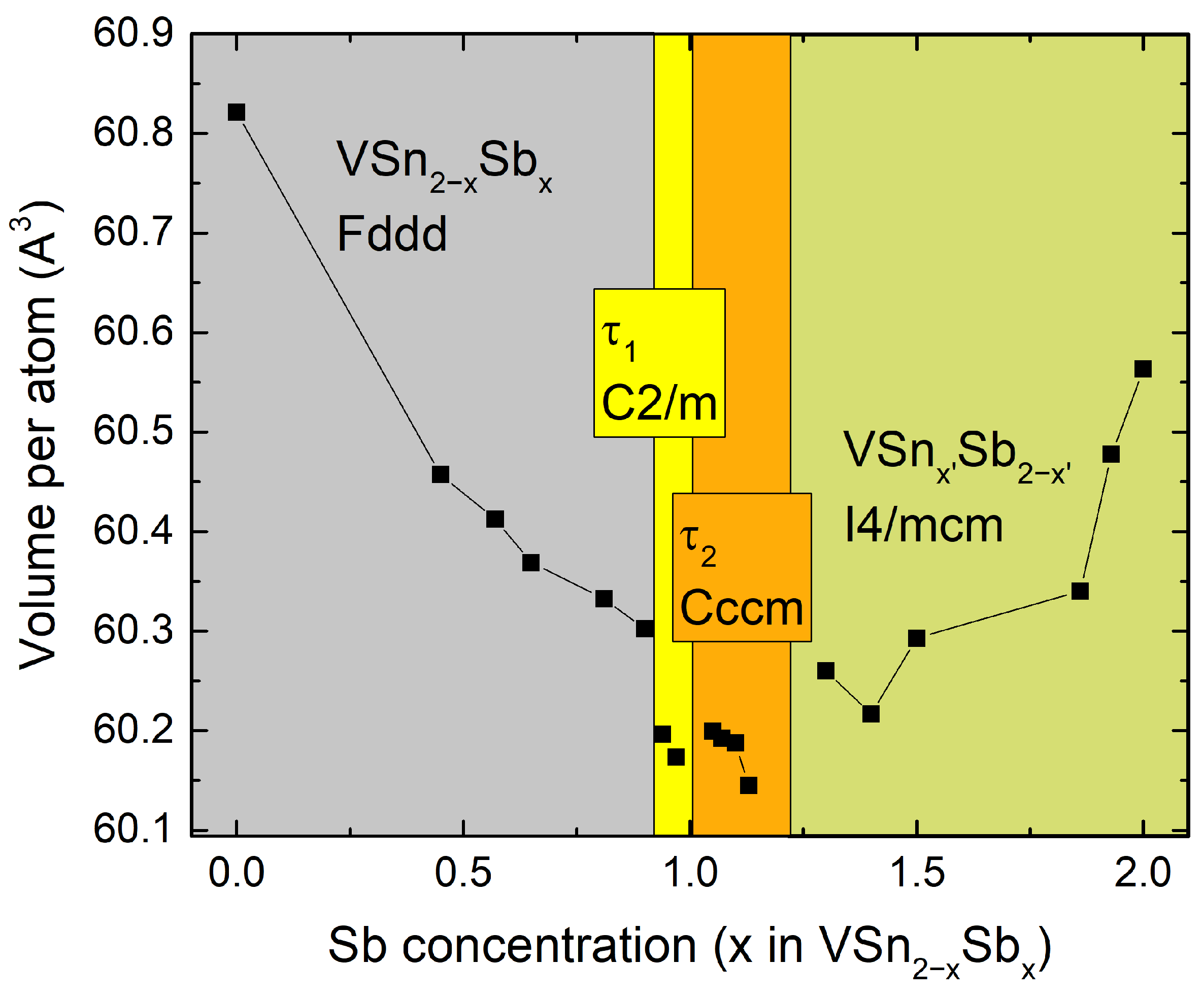
The normalized unit cell volume of the compounds at room temperature versus the composition is shown in Figure 1. It is interesting to note that the volume per atom does not change monotonically from VSn2 to VSb2. The volume initially decreases with the increasing Sb content, goes through several discontinuities due to the formation of the τ1 and τ2 phases, and reaches a minimum at approximately 62.5% VSb2, after which it increases, excluding the anomaly at VSb1.4Sn0.6. While the volume decrease could be expected given the smaller size of the Sb atoms, its increase in the Sb-rich region appears to go against that notion. The volume increase in the VSnx′Sb2−x′ solution is attributed to the increase in the c parameter, while the a(b) parameter expectedly increases (Figure S2 in Supporting Information). Both of these processes occur monotonically, but not linearly, and hence, the somewhat erratic changes in volume with the “abnormal” minimum at VSb1.4Sn0.6. The c parameter in VSnx′Sb2−x′ is determined by the V-V distances. The latter is a result of the changes in the chemical bonding between VSn2 and VSb2, which will be discussed in the corresponding sections below.
Figure 1.
Changes in the normalized (per atom) unit cell volumes of VSn2−xSbx, τ1, τ2, and VSnx’Sb2−x′ (where x′ = 2 − x) at room temperature as determined from powder XRD. The lines are drawn to guide the eye.
3.2. Crystal Structure of V(Sn, Sb)2 Phases
Given that the crystal structures of the new ternary phases derive themselves from those of the binary compounds and their solid solutions, it seems reasonable to discuss first the structure features of the former. The crystallographic data for all compounds are given in Table 1 and Table 2. The most important interatomic distances are summarized in Tables S2 and S3 in the Supporting Information.
Table 1.
Crystallographic and refinement parameters for the Mn4Al11 single crystal obtained from the Mn4Al11Sn44 sample.
Table 2.
Atomic coordinates and displacement parameters for the V(Sn, Sb)2 single crystals. The occupancies of the sites were constrained at selected values based on the EDX results and crystal chemical considerations (see text and Supporting Information).
While the VSn2−xSbx and VSnx’Sb2−x′ solid solutions possess the same structure types as their parent binary phases, the interatomic distances noticeably change from those of the parent compounds.
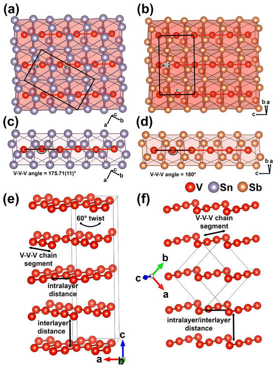
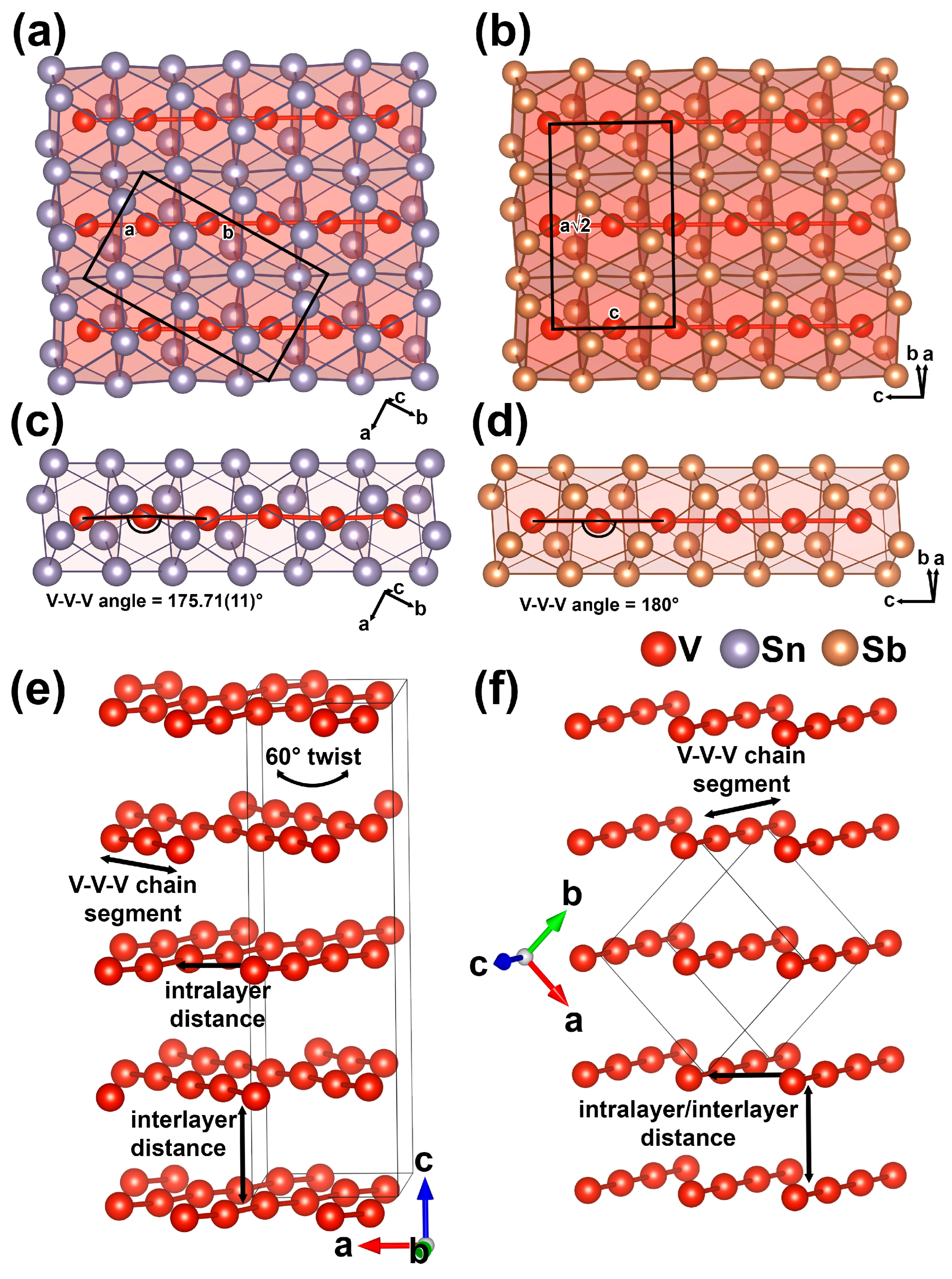
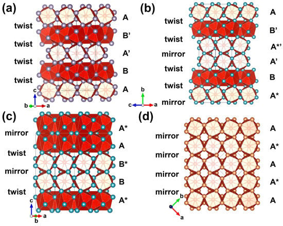
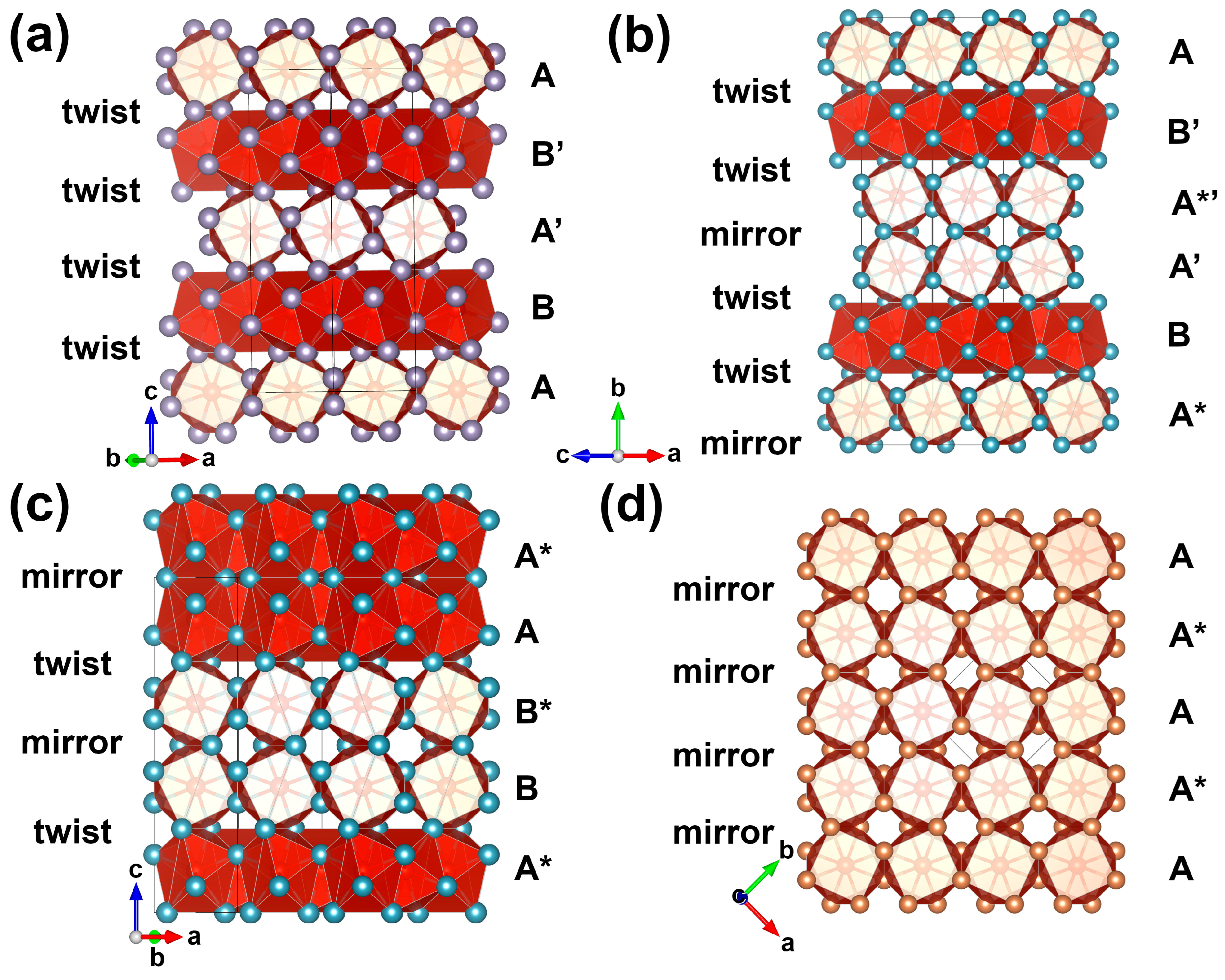
The crystal structure of VSn2 and its solid solution VSn2−xSbx can be represented as layers of VE8 (E = Sn, Sb) antiprisms (Figure 2 and Figure 3) merged along their bases and their side edges, creating almost linear parallel chains of V atoms (Figure 2c,e). The layers are twisted by 60° with respect to each other in a ABA′B′ pattern. The first layer (A) is shifted by 30° clockwise with respect to the b axis. The second layer—layer B—is rotated by 60° counter-clockwise with respect to layer A or by 30° counter-clockwise with respect to the b axis (Figure 2e). The layers A′ and B′ are almost identical to the corresponding layers A and B but are shifted by a/2 with respect to the latter ones.
Figure 2.
Layers of coupled VSn8 (a) and VSb8 (b) antiprisms in the crystal structures of VSn2 and VSb2, respectively, single V chains enclosed in the Sn (c) and Sb (d) columns, and arrangements of V chains in the crystal structures of VSn2 (e) and VSb2 (f).
Figure 3.
Fragments of the VSn2 (a), τ1 (b), τ2 (c), and VSb2 (d) crystal structures, showing layers of VE8 square antiprisms. The V atoms are shown in red; the Sn and Sb atoms are grey and orange, respectively; mixed Sb/Sn sites (E) in τ1 and τ2 are given in pale blue. The symbols A, A*, A’, A*’, B, B* and B’ denote different sorts of layers. The layers of A- and B-type are rotated by 60° with respect to each other. The symbol (*) indicates a layer that mirrors the neighboring layer of A- or B-type, while the symbol (’) indicates that the layer is shifted by a/2 with respect to a layer of the same type (A or B).
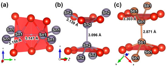
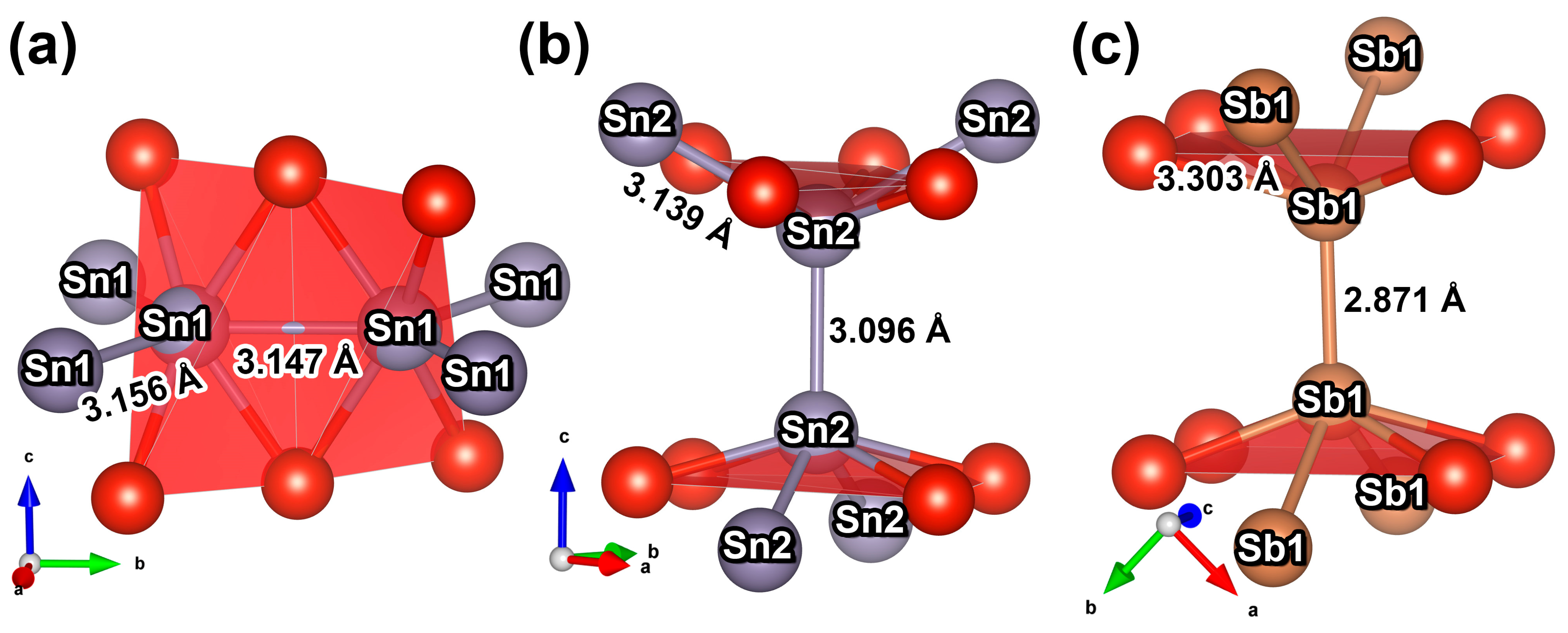
In comparison to VSn2, the VSn2−xSbx solid solution features a smaller unit cell, mostly due to the compression along the a axis as V chains within the layer are brought closer to each other. Surprisingly, this is not a result of the shortening of the V-Sn bonds due to Sb doping, as the V-Sb bonds in VSb2 are even longer than their V-Sn counterparts in VSn2, being 2.839 Å versus 2.824 Å on average, respectively. The contraction of the unit cell is rather a result of the Sn2-Sn2 bond contraction due to the Sb for Sn partial substitution. The length of the Sn2-Sn2 (E2-E2) bond changes from 3.0963(9) Å in the binary phase (Figure 4b) to 2.9351(8) Å in VSn1.35Sb0.65 and 2.9114(7) Å in VSn1.1Sb0.9, which is quite close to the 2.8708(5) Å distance of the Sb-Sb bond in VSb2, suggesting a significant Sb concentration in the E2 site.
Figure 4.
The coordination environments of the Sn1 (a) and Sn2 (b) atoms in VSn2 and of the Sb atoms (c) in VSb2. The standard uncertainties of the given distances do not exceed 0.002 Å. The V atoms are shown in red; the Sn and Sb atoms are grey and orange, respectively.
Despite the significant contraction of the E2-E2 dumbbell, which lies perpendicular to the c direction, the c parameter and the corresponding distances between the V chains from different layers (c/4) not only do not decrease, but instead significantly increase upon going from VSn2 to VSn1.3Sb0.65 or VSn1.1Sb0.9. Thus, the V chains within the layers are brought closer to each other to maintain V-E2 distances, which remain practically identical to those in VSn2. The expansion of the unit cell in the c axis is the result of the increased V-Sn1 (V-E1) distance. In the solid solution, the latter stretches to 2.7955(10) Å from the initial 2.7665(12) Å in VSn2. The increased V-E1 distance may be a sign of the Sb presence in this position as well, as the V-Sb bonds are expected to be longer than the V-Sn ones in these compounds. The Sb at the E1 site is also suggested by the difference between the E1-E1 and Sn1-Sn1 distances, with the longer and shorter E1-E1 distances being inverted compared to the Sn1-Sn1 counterparts (See Table S2 in Supporting Information).
The increased V-E1 distance also leads to the straightening of the V chains. As the shortest intralayer V-V distance between the chains remains almost the same (4.749(3) Å in VSn2, 4.745(4) Å in VSn1.35Sb0.65, and 4.738(3) Å in VSn1.1Sb0.9), the V-V-V angle increases from 175.71(13)° in VSn2 to 177.59(13)° in VSn1.35Sb0.65, and 177.90(10)° in VSn1.1Sb0.9, which pushes the chains away from each other, where they do not intersect. As a result of the increased V-V-V angle, the V-V distance in the chains decreases from 2.7310(3) Å (VSn2) to 2.72322(18) Å (VSn1.1Sb0.9). A somewhat similar effect of flattening of the transition metal sublattice was observed in our investigation of the α-Fe6Ga5 and Fe6Ge5 compounds [6,27], where the highly corrugated Fe layers in the Ga-based phase become almost flat in the Ge-based counterpart.
As the short Sn2-Sn2 bonds become shorter upon Sb doping, the longer Sn2-Sn2 bonds are stretched from 3.1388(5) Å to 3.2395(5) Å (VSn1.35Sb0.65) and 3.2514(4) Å (VSn1.1Sb0.9), which is close to the longer Sb contacts in VSb2 of 3.3024(4) Å (Figure 4b,c).
Although we could not discern between Sn and Sb atoms in our X-ray diffraction experiments, we believe that the Sb atoms primarily occupy the E2 site, whereas the E1 site features only a limited amount of the Sb atoms, as this coordination is not characteristic of the latter. While a somewhat similar elongated SbV4 tetrahedron is featured in V8-δSb9, the V-Sb bonds in it are much shorter (2.745(2) Å) [28], and the Sb atom in its center is not surrounded by other Sb atoms. For comparison, V-Sn1 (V-E1) distances are 2.79–2.82 Å in VSn2 and VSn2−xSbx, while the Sn1 (E1) site in VSn2 and VSn2−xSbx is neighbored by three other Sn1 (E1) atoms (Figure 4a). This is also the likely reason why the crystal structure, upon higher Sb doping, transforms into that of the τ1 phase with a lower number of twists per layer, as the Sn1-type positions are responsible for creating the twists. Based on the comparison of the interatomic distances in our compounds and their chemical composition, we believe that the highest Sb/Sn ratio in the E1 site should be approximately 0.3/0.7 (see Supporting Information), after which the twist is replaced with a mirror-type joint.
The earlier investigation of the isostructural phase TiSnSb [15] supports this conclusion. The results of the crystal structure analysis performed by the authors suggest that the Sn atoms prefer the Sn1 (E1) site, while the Sb atoms prefer the Sn2 (E2) site. Their electronic structure analysis showed that this model is more stable than the one with reversed Sb and Sn ordering.
On the other side of the VSn2-VSb2 section, VSb2 (Figure 2b,d,f and Figure 3d) forms a solid solution VSnx′Sb2−x′. Since there is only one p-element site in its crystal structure, the Sb and Sn simply mix there. As a result of the Sn for Sb partial substitution, the E-E distances and V-V distances noticeably change, while the V-E distances remain almost the same. The length of the short E-E bond in the solid solution increases to 2.9014(6) Å (VSn0.7Sb1.3), which is close to that of the short E2-E2 bonds in VSn1.1Sb0.9. On the other hand, the longer E-E contacts of 3.3030(5) Å shrink to 3.2655(5) Å (VSn0.6Sb1.4) and 3.2544(4) Å (VSn0.7Sb1.3), which is also similar to their counterparts in the VSn2-based solution. The V-V distances experience more dramatic changes going from 2.8031(5) Å in VSb2 to 2.7485(4) in VSn0.6Sb1.4 and to 2.7360(3) Å in VSn0.7Sb1.3.
As was mentioned above, between the two solid solutions, two ternary phases form, creating a gradual transition from one structure type to another. At higher Sn concentrations, the τ1 phase is formed, which possesses a monoclinic structure (Figure 3b). This structure is unique to the V-Sn-Sb system and is a new variation in the CuAl2-CuMg2-NiMg2 structural family. The τ1 phase features the same basic building blocks of VSn2 and VSb2 arranged in a different order. The layers of VE8 antiprisms are conserved, but their order is changed. The layers are now stacked in the AA*BA′A*′B′ pattern with two twists per three layers (Figure 3b). The A and A* layers are mirrored versions of each other, so are the A′ and A*′ layers. The A′ layer is shifted by a/2 with respect to the A layer, the B and B′ layers being similarly related. The double AA* and A′A*′ layers are essentially fragments of the CuAl2 type, breaking the normal CuMg2-type sequence. Thus, 1/3 of the twists are replaced by mirror joints from the CuAl2 type.
Given that there are two types of layer joints, the environments of some E sites resemble that of the Sn atoms in VSn2 (Figure 4a,b), while the other is more similar to that of the VSb2 (Figure 4c). The E1 sites are located within the twists and share the Sn1-type of coordination, while the E4 and E5 sites form the E4-E5 dumbbells supported by two V4 rectangles twisted with respect to each other, similar to the Sn2 atoms in VSn2. The E2 and E3 sites are located within the AA* and A′A*′ blocks and share the environment of the Sb atoms in VSb2.
The distances in the center of the AA* and A′A*′ blocks are similar to those in the VSnx′Sb2−x′ solid solution, while the distances in the B and B′ layers are expectedly closer to those found in VSn2−xSbx (Table S3 in Supporting Information). In particular, the lengths of the shorter E2-E2 and E3-E3 bonds in the AA* (A′A*′) block are 2.9254(11) Å and 2.9114(13) Å, respectively, while the longer E3-E3 and E2-E4 contacts are 3.2405(13)/3.2443(13) Å and 3.2502(9) Å, respectively, suggesting a high concentration of Sb in the E2-E4 sites. The E2-E2 bond is slightly longer; hence, we assume a slightly higher Sn concentration in this position. The E4-E5 distance on the A′B boundary is also quite short, 2.9115(11) Å, suggesting a high Sb content. This leaves only the E1 site located in the twists as the site with the majority of Sn atoms. The length of the E1-E1 bonds in the τ1 phase is close to that of the Sn1-Sn1 (E1-E1) bonds in VSn2−xSbx and VSn2, although the former ones are slightly shorter.
Compared to those in VSn2−xSbx, the V chains are further straightened in τ1, the angles being slightly larger in the former in both the twisted B-type layers (177.69(15)°) and the normal A-type layers (178.99(11)°).
At higher Sb concentrations, the orthorhombic τ2 phase is formed (Figure 3c). Although it shares the unit cell dimensions with VSn2 and its solid solution, it features a different crystal structure with the AA′BB′ order of layers instead of ABA′B′ one. Thus, the number of twists is reduced by half compared to VSn2, creating two double layer blocks of the CuAl2 type stacked on top of each other and twisted by 60°. This continues the trend of reducing the number of twists per layer upon Sb doping, with only half of the twists remaining in τ2.
The atomic environments and the interatomic distances themselves in the twisted fragments and in the center of the CuAl2 type blocks expectedly resemble those in similar fragments in other phases (Table S2 in Supporting Information). The E1 atoms occupy the Sn1 type position, while the E1-E1 distances (3.1227(3) Å and 3.1508(6) Å) at the A′B and B′A boundaries are close to the Sn1-Sn1 distances in VSn2, suggesting primarily Sn occupation. The E2 atoms are also located within the VSn2-type twist and form E2-E2 dumbbells.
The distances between the E2, E3, and E4 atoms are closer to the E-E distances in VSnxSb2−x or the Sb-Sb distances in VSb2, indicating that these sites are occupied mostly by Sb atoms. The V-V-V angles also increase further to 179.00(7)°, straightening the V chains even more.
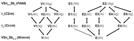
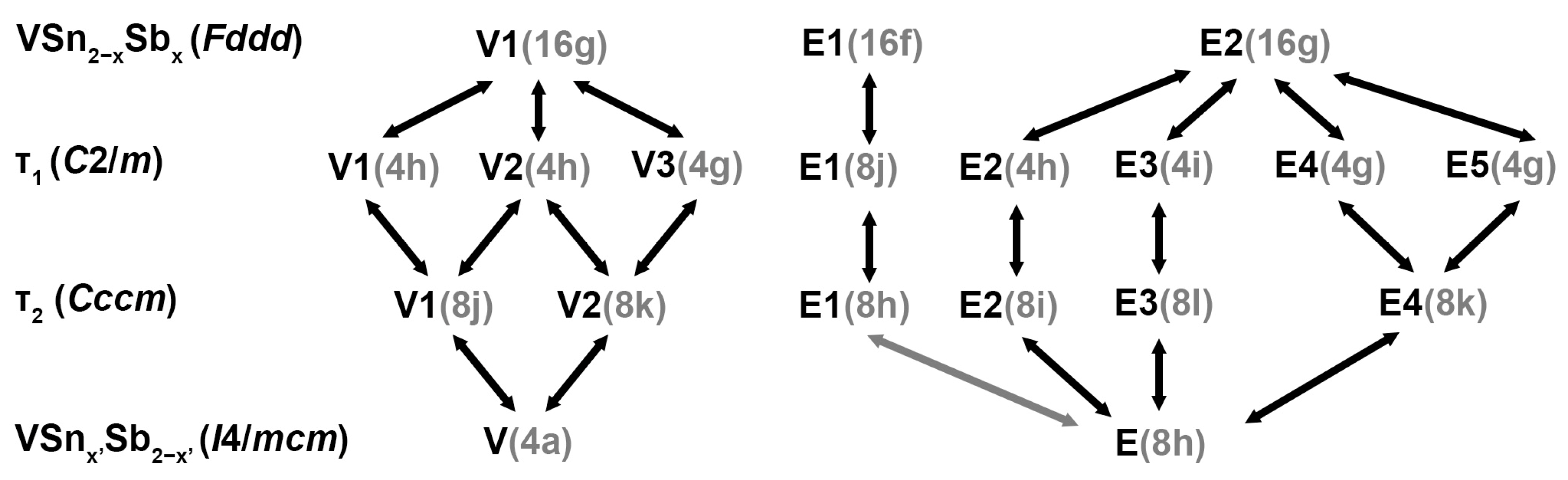
The structural evolution and the relationships between different crystallographic positions can be summarized in Figure 5. The V atoms are always coordinated by square antiprisms, and there are very small differences in the overall geometry of this polyhedron upon going from VSn2 to VSb2. Thus, there is essentially only one type of V atom in the obtained phases. The Sn/Sb sites or E sites experience more interesting changes. Going from VSn2−xSbx to τ1 and τ2, the E1-type or Sn1-type position is conserved, while the E2 site splits into several independent positions. The latter reconverge into a single E site in VSnx′Sb2−x′. VSnx′Sb2−x′ also does not feature a direct analogue of the Sn1-type site, since there are no twists present in it. However, the coordination of the E1 atoms and the Sb atoms are still related and differ, in principle, only by the shift of the V atom from the V4 rectangle (Figure 4).
Figure 5.
The relationships between the atomic positions in different V(Sn, Sb)2 phases.
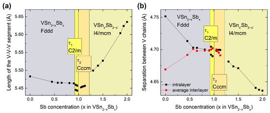
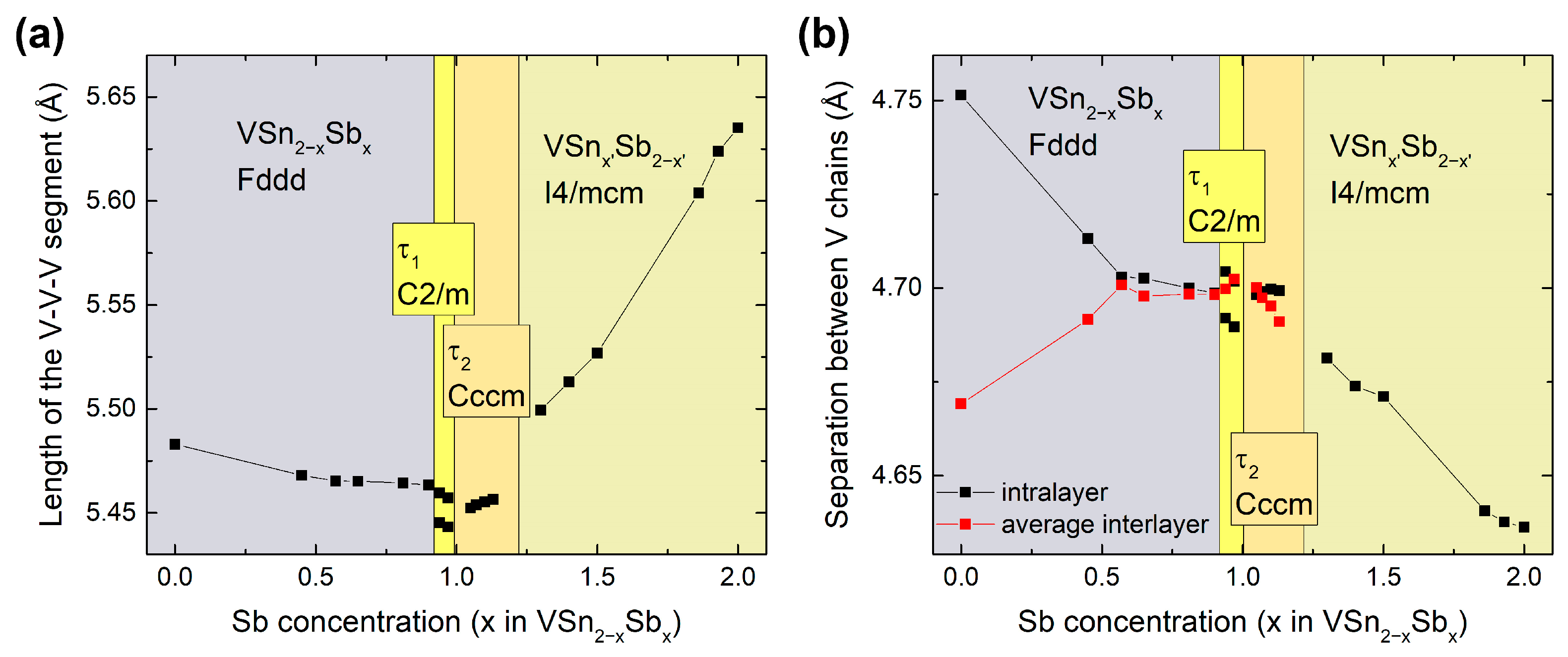
Although our powder X-ray diffraction data were not suitable for structural analysis, the determined unit cell parameters at room temperature still provide us with another important perspective on the structural evolution in this system. While we cannot directly compare the unit cell parameters between all the compounds, since the size of the unit cell can be significantly different between them due to the different crystal systems, we can still normalize these values to the dimensions of the basic structure blocks. The length of the V chain segments and the separations between the chains were found to be particularly useful and demonstrative parameters that can be calculated directly from the unit cell parameters.
Going from the VSn2 to VSb2, the length of the V-V-V chain segment (Figure 2e,f) slightly decreases at first upon increasing Sb content and then increases in the τ2 and VSnx′Sb2−x′ phases (Figure 6a). In the τ1 phase, the V chains split into two different types of V chains with different periods, with the first one being closer to those in VSn2−xSbx, while the second being closer to those in the τ2 phase.
Figure 6.
Changes in the length of the V-V-V chain segments (a) and the separation between the V chains (b) in VSn2−xSbx, τ1, τ2, and VSnx′Sb2−x′ (where x′ = 2 − x) at room temperature as determined from powder XRD. The lines are drawn to guide the eye.
Although the distances between the V atoms from different chains require the knowledge of the exact positions of the V atoms, the distances (or the averaged distances) between the chains themselves (Figure 6b) can be calculated just from the unit cell dimensions. As was mentioned above, upon Sb doping in VSn2−xSbx, the intralayer distance between the chains decreases, while the interlayer one increases (Figure 2e). As can be seen in Figure 6b, the two distances are actually brought together at approximately x ~ 0.6, after which they stay very close up until the formation of the VSnx′Sb2−x′ solid solution, where they even merge (Figure 2f), due to the tetragonal symmetry of the latter. Thus, the Sb-doping appears to make the structure more isotropic, even if the overall symmetry of the structure does not require it. The exact reason behind this is not fully clear; however, it might be caused by the difference in the character of V-Sb and V-Sn interactions, which will be discussed in the following section.
It is also interesting to note that amongst the obtained phases there is no crystal structure of the NiMg2 type, frequently observed as an intermediate step between the CuMg2- and CuAl2-type structures [10,11]. In those cases, however, the substitution occurred in the d-metal sublattice, not in the p-element one. Given that the number of twists per layer is the same in NiMg2 and CuMg2, the appearance of NiMg2-type in those cases might be due to two different transition metal sites, allowing partial or complete ordering of two different d-metals, which can help in resolving structural stresses.
3.3. Electronic Structure Analysis of VSn2 and VSb2
In order to gain a deeper understanding of the structural changes in the VSn2-VSb2 pseudo-binary section, we have performed a real-space analysis of the VSn2 and VSb2 electronic structure using the electron localization function (ELF) and crystal-orbital Hamilton population (COHP). Both ELF and COHP analyses show significant changes in the chemical bonding between the two compounds.
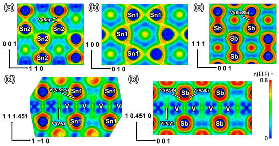
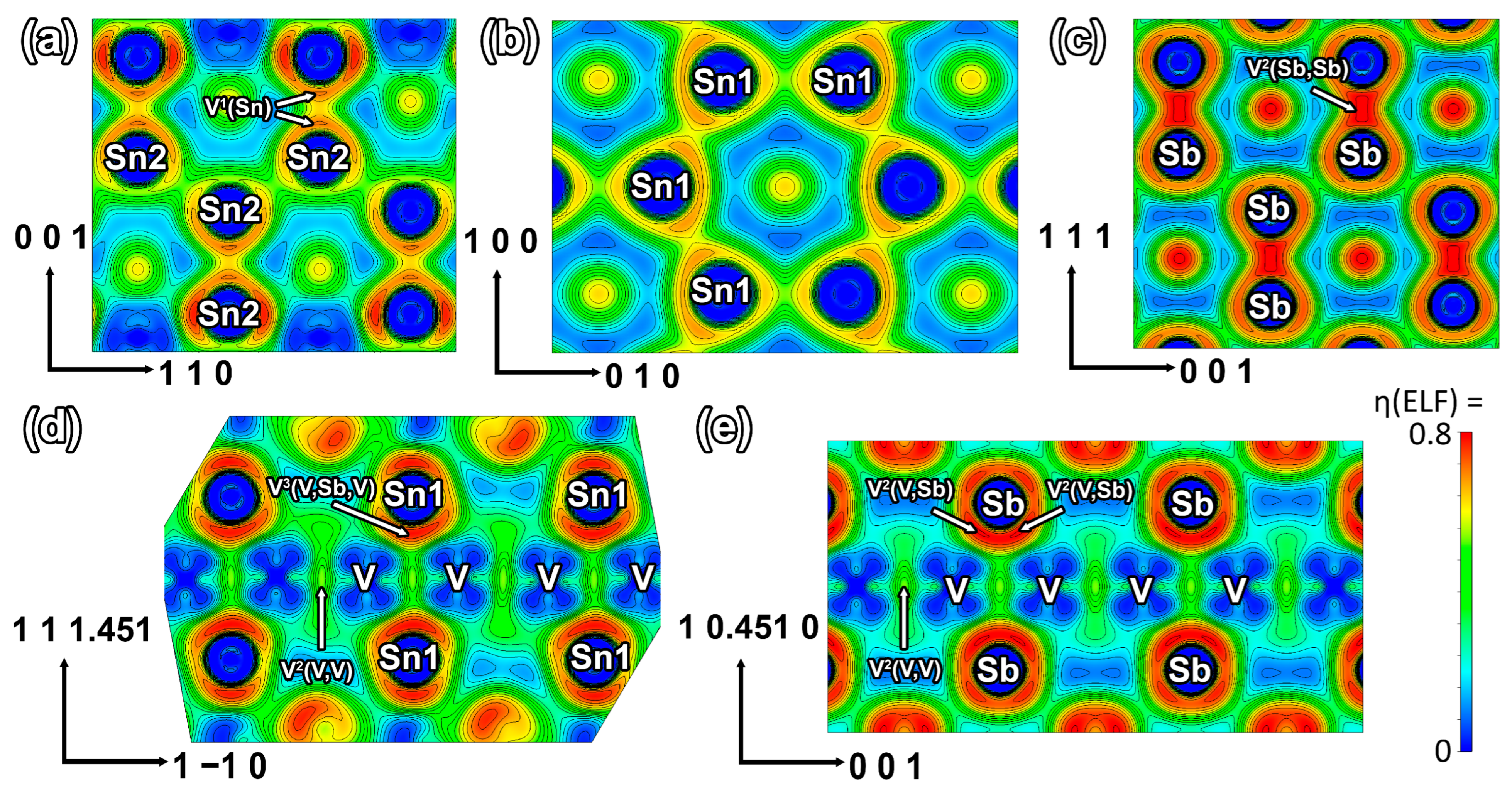
The ELF sections of the V-V, V-Sb, and V-Sn bonds showing main ELF attractors clearly point to a different character of the V-Sb and V-Sn interactions (Figure 7d,e). Whereas V-Sb bonds show a separate ELF attractor for each bond, V-Sn bonds share one attractor between two V-Sn contacts, signaling three-center interactions. As Sn has one electron less compared to Sb, the V-Sn interactions are optimized by bringing V atoms closer, which strengthens the available bonding interactions and reduces their number. Hence, we observe a reduction in the V-V distance upon Sn doping in VSb2.
Figure 7.
Cross-sections of the ELF distribution near the Sn2-Sn2 dumbbells in VSn2 (a), the Sn1 honeycomb nets in VSn2 (b), the Sb-Sb dumbbells in VSb2 (c), and the V chains in VSn2 (d) and VSb2 (e). The ELF attractors are marked with white arrows. The basis vectors of the planes are shown by black arrows.
It is worth mentioning that an earlier investigation of the chemical bonding in VSb2 revealed only one ELF attractor in the V-Sb-V bridges, instead of two [8]. This may be due to the different computational parameters used, such as the basis and/or functional, since our attempts to use the same crystal structure parameters obtained at room temperature by the authors [8] still led to two resolved attractors.
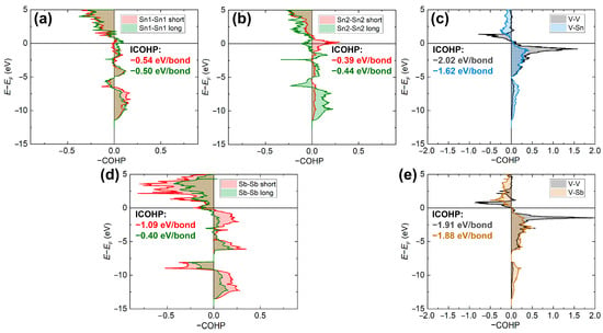
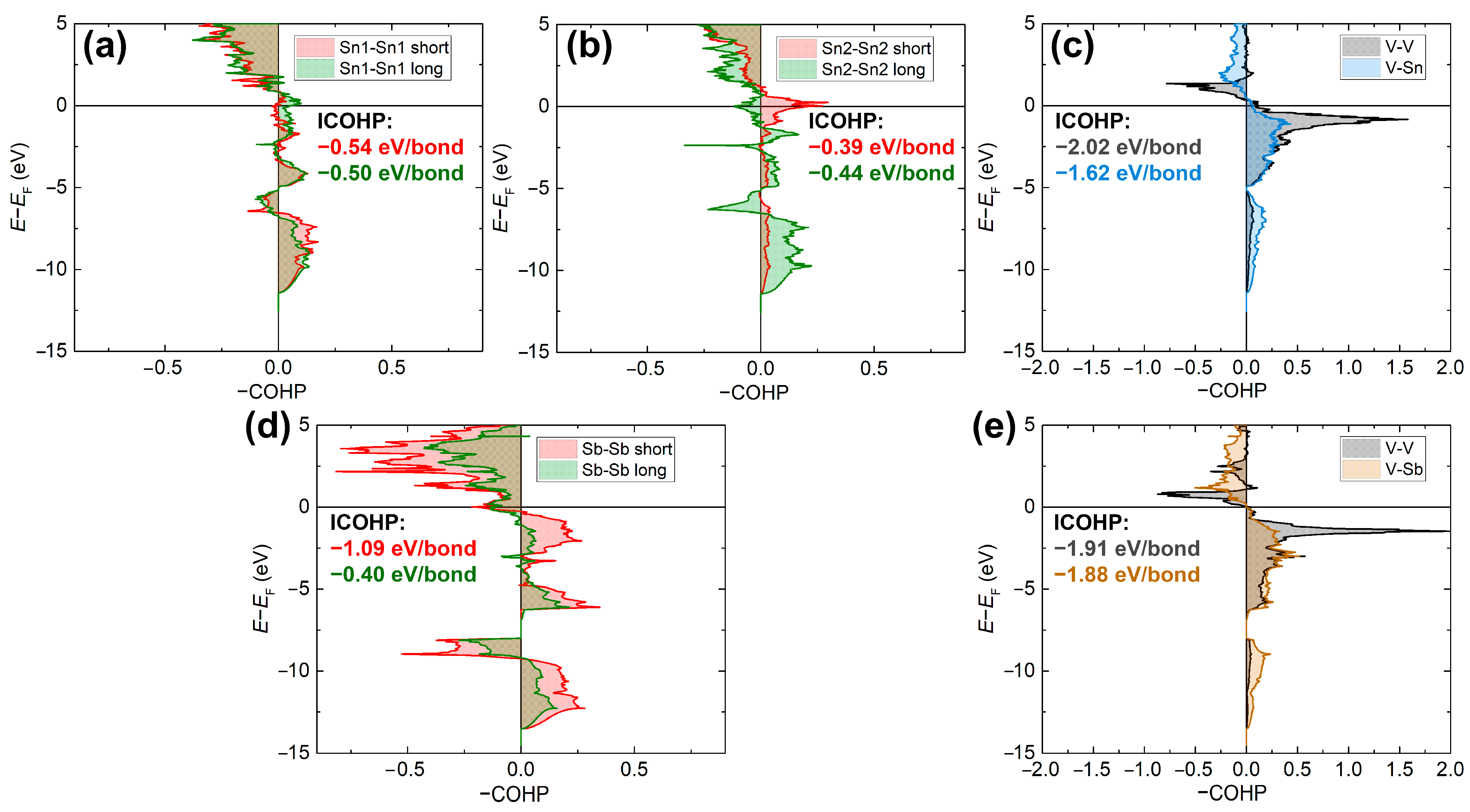
The character of Sb-Sb and Sn-Sn bonds also noticeably differs. The short Sb-Sb bonds display high values of ELF and show one attractor with η = 0.81 in the middle of the bond (Figure 7c), while the longer Sb-Sb contacts exhibit only a saddle point with a much lower η of 0.36. The COHP function shows that the short Sb-Sb bonds are well optimized, whereas the longer ones are not, with mostly nonbonding regions below the Fermi level (Figure 8d). The difference might stem not only from the difference in the interatomic distances, as the latter is the consequence of the optimization of the bonding, but rather due to the V atoms that bridge the longer Sb-Sb contacts. The electronic system appears to optimize the V-Sb interactions, as can be seen in Figure 8e.
Figure 8.
COHP diagrams calculated for the Sn1-Sn1 (a), Sn2-Sn2 (b), V-V, and V-Sn (c) interactions in VSn2, and for the Sb-Sb (d), V-V, and Sb-Sb (e) in VSb2.
Conversely, different Sn-Sn bonds in VSn2 are much more similar to each other, with all the bonds showing saddle points in the middle with η = 0.52–0.63 (Figure 7a,b). The short Sn2-Sn2 bonds do exhibit two attractors with η of 0.70, but they are closer to individual Sn2 atoms. The distribution of the electron density is also very similar between different Sn-Sn bonds, with saddle points at ρ of 0.19 e−/Å3 (Figure S3 in Supporting Information). Nevertheless, there seems to be an inverse correlation between the number of V atoms bridging the Sn-Sn bonds and the ELF values.
The COHP analysis shows that the short Sn2-Sn2 bonds are surprisingly weak, accounting for ICOHP of only −0.31 eV, whereas even the longer Sn2-Sn2 contacts produce ICOHP of −0.58 eV each (Figure 8b). The weakness of the short Sn2-Sn2 bonds is caused by not fully occupied bonding states near the Fermi level. The COHP graphs show that the V-Sn bonds are well optimized (Figure 8c), which the system appears to prioritize, given the number of available electrons.
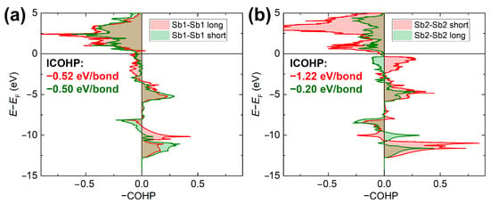
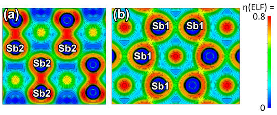
The short Sn2-Sn2 bonds can be optimized by replacing the Sn atoms with Sb, which occurs in the solid solution VSn2−xSbx (Figure 9b and Figure 10a). The replacement of Sn by Sb atoms maintains the optimized V-E interactions, while the short E2-E2 interactions are now optimized as well because Sb atoms have one electron more and their energy is lower compared to Sn atoms. The electrons can be supplied to the system in the other way—by replacing the V atoms with heavier 3d metals, such as Mn, Fe or Co, which stabilizes the short Sn-Sn bonds and transforms the structure into the CuAl2 type [10], providing the same end result as the Sb doping.
Figure 9.
COHP diagrams calculated for the Sb-Sb interactions in the two hypothetical ordered models of VSn2−xSbx with the E1 (a) or E2 (b) sites being fully occupied by Sb atoms. The cell parameters and atomic coordinates were taken from VSn1.1Sb0.9 for these calculations.
Figure 10.
Cross-sections of the ELF distribution near the E2-E2 dumbbells and the E1 honeycomb nets in the two hypothetical ordered models of VSn2−xSbx with the E2 (a) or E1 (b) sites being fully occupied by Sb atoms.
While the Sb atoms can stabilize the Sn2-Sn2 interactions, they are poorly suited to the environment of the Sn2 type inside the honeycomb nets (Figure 9a and Figure 10b), preferring to form unbridged and short covalent Sb-Sb bonds. Thus, the crystal structure gradually transitions to the CuAl2 type, keeping some of the Sn1 and Sn2 positions within the twists up until the very high Sb concentration.
This situation in some way resembles that in the related Fe32+δGe35-xEx phases (E = Si, P, As) [29,30,31,32]. The As-based phase—Fe32+δGe33As2—is stabilized by the inclusion of As-As dumbbells, as the Ge-Ge dumbbells need to be supported by additional Fe atoms (δ) above and/or below them, which destabilizes the structure [29,30]. The latter can be alleviated by Si- and P-doping, and Ge-Ge dumbbells along with partial occupation of the neighboring Fe site (δ = 0.5–1) are observed in the Si- and P-based phases [30,31,32].
4. Conclusions
The V(Sn, Sb)2 phases have been isolated and studied using both experimental and theoretical methods. These compounds are built from layers of coupled VE8 antiprisms (E = Sn, Sb) that are either parallel or twisted with respect to each other. Our crystal structure analysis revealed a gradual structural transformation occurring between VSn2 (CuMg2-type) and VSb2 (CuAl2-type), with solid solutions VSn2−xSbx and VSnx′Sb2−x′ separated by two ternary phases τ1 and τ2 serving as intermediate steps between two binary compounds.
While the initial Sb-doping stabilizes the CuMg2-type structure by forming the Sb-Sb or Sb-Sn dumbbells, Sb atoms with one additional valence electron are not well suited for the environment of the Sn honeycomb nets, which are a necessary portion of the twists. Hence, going from VSn2 to VSb2, the number of twists between layers gradually reduces from one to zero, with intermediate steps at 2/3 (τ1) and 1/2 (τ2).
Not all the structural changes cause major structural transformations. The Sb doping also causes more subtle, but just as important, changes to the distances inside and between the V chains. Upon Sb doping, the intralayer and interlayer distances between the chains become more similar, while the chains themselves straighten. The latter causes the initial decrease in the V-V distances in the chains, which then increases in the VSnx′Sb2−x′ solid solution. Our theoretical calculations show that the V-V distances evolve as a result of the change in the character of the V-E interactions from 3-center bonds in VSn2 to 2c-interactions in VSb2.
The results of this research show that p-element doping can be a powerful tool to tailor the structure of the intermetallic phases and stabilize the desired crystal structures. The differences in the electronic configuration of p-elements also force them to occupy different positions within the structure, allowing complex intergrowth structures to form.
Given the nontrivial topology of the electronic structure of VSb2 leading to unusual transport and magnetotransport properties [33,34], including high magnetoresistance, the electronic structure and the transport properties of the obtained V(Sn, Sb)2 phases await an experimental investigation.
Supplementary Materials
The following supporting information can be downloaded at: https://www.mdpi.com/article/10.3390/cryst16100623/s1; Figure S1: Electron microphotographs (secondary electrons) of the obtained crystals from samples with the following initial compositions: VSn8.75Sb1.25 (a), VSn7.5Sb2.5 (b), VSn3Sb2 (c), and VSn2.5Sb2.5 (d); Figure S2: Cell parameters of VSnx’Sb2−x’ versus Sb content (2–x’) at room temperature as determined from powder XRD. The lines are drawn to guide the eye; Figure S3: Cross-sections of the electron density distribution near the Sn2-Sn2 dumbbells (a) and the Sn1 honeycomb nets (b) in VSn2; Table S1: Initial composition and results of the powder XRD and EDX analyses. The elemental compositions are normalized to two p-element atoms per formula, since the V concentration was frequently overestimated in our EDX analysis, due to incorrect quantitative corrections owing to the large difference in the atomic number between V and Sn or Sb; Table S2: Most important interatomic distances in VSn2, VSb2, and their solid solutions; Table S3: Most important interatomic distances in τ1 and τ2.
Author Contributions
Conceptualization, R.A.K. and A.V.S.; methodology, R.A.K., K.A.L. and A.V.S.; validation, R.A.K. and K.A.L.; formal analysis, R.A.K., A.R.E. and K.A.L.; investigation, R.A.K., A.R.E., K.A.L., A.O.P. and A.N.K.; resources, A.V.S.; data curation, R.A.K.; writing—original draft preparation, R.A.K.; writing—review and editing, R.A.K. and A.V.S.; visualization, R.A.K.; supervision, A.V.S.; project administration, A.V.S.; funding acquisition, A.V.S. All authors have read and agreed to the published version of the manuscript.
Funding
This research was funded by the Russian Science Foundation, grant number 25-13-00005.
Data Availability Statement
The original contributions presented in this study are included in the article/Supplementary Materials. Further inquiries can be directed to the corresponding author.
Acknowledgments
Access to a Bruker D8 QUEST diffractometer has been provided by the Development Program of Lomonosov Moscow State University.
Conflicts of Interest
The authors declare no conflicts of interest.
References
- Yannello, V.J.; Fredrickson, D.C. Generality of the 18−n rule: Intermetallic structural chemistry explained through isolobal analogies to transition metal complexes. Inorg. Chem. 2015, 54, 11385–11398. [Google Scholar] [CrossRef] [Scilit] [PubMed]
- Likhanov, M.S.; Shevelkov, A.V. Intermetallic compounds with non-metallic properties. Rus. Chem. Bull. 2020, 69, 2231–2255. [Google Scholar] [CrossRef] [Scilit]
- Verchenko, V.Y.; Likhanov, M.S.; Kirsanova, M.A.; Gippius, A.A.; Tkachev, A.V.; Gervits, N.E.; Galeeva, A.V.; Buttgen, N.; Kratschmer, W.; Lue, C.S.; et al. Intermetallic solid solution Fe1−xCoxGa3: Synthesis, structure, NQR study and electronic band structure calculations. J. Solid State Chem. 2012, 194, 361–368. [Google Scholar] [CrossRef] [Scilit]
- Kitagawa, J.; Yakabe, G.; Nakayama, A.; Nishizaki, T.; Tsubota, M. Competition between ferromagnetic and antiferromagnetic states in Al8.5−xFe23Ge12.5+x (0 ≤ x≤ 3). J. Solid State Chem. 2020, 284, 121188. [Google Scholar]
- Khalaniya, R.A.; Mironov, A.V.; Kulchu, A.; Khrykina, O.; Shevelkov, A.V. Disorder-and magnetism-driven structural changes in Sm2Mn1–xGa6–yGey. Acta Cryst. B 2025, 81, 235–243. [Google Scholar]
- Khalaniya, R.A.; Verchenko, V.Y.; Zonov, E.M.; Stern, R.; Shevelkov, A.V. Crystal structure, chemical bonding, and magnetism of α-Fe6Ga5: How local interactions shape the structure and properties of intermetallic compounds. Inorg. Chem. 2024, 63, 21099–21109. [Google Scholar] [CrossRef] [Scilit] [PubMed]
- Plenkin, D.S.; Azarevich, A.N.; Bogach, A.V.; Polevik, A.O.; Verchenko, V.Y.; Shevelkov, A.V. Crystal structure, electronic structure, and physical properties of three novel intermetallic compounds MoSb2−xEx (E = Ga, Ge, Sn), representatives of the OsGe2-type structure. J. Alloys Compd. 2026, 1067, 188488, Correction in J. Alloys Compd. 2026, 1055, 186511. [Google Scholar] [CrossRef] [Scilit]
- Armbruester, M.; Schnelle, W.; Schwarz, U.; Grin, Y. Chemical bonding in TiSb2 and VSb2: A quantum chemical and experimental study. Inorg. Chem. 2007, 46, 6319–6328. [Google Scholar] [CrossRef] [Scilit] [PubMed]
- Wölpl, T.; Jeitschko, W. Crystal structures of VSn2, NbSn2 and CrSn2 with Mg2Cu-type structure and NbSnSb with CuAl2-type structure. J. Alloys Compd. 1994, 210, 185–190. [Google Scholar] [CrossRef] [Scilit]
- Häussermann, U.; Simak, S.I.; Abrikosov, I.A.; Johansson, B.; Lidin, S. Electronically induced phase transitions in ternary transition metal distannide systems. J. Am. Chem. Soc. 1998, 120, 10136–10146. [Google Scholar] [CrossRef] [Scilit]
- Larsson, A.K.; Lidin, S. The crystal structures of the closely related CrSn2, NiCr5Sn12 and NiCr3Sn8 phases. J. Alloys Compd. 1995, 221, 136–142. [Google Scholar] [CrossRef] [Scilit]
- Tkachuk, A.V.; Akselrud, L.G.; Stadnyk, Y.V.; Bodak, O.I. Isothermal section of the Ti–Mn–Sn system and crystal structure of the TiMnSn4 compound. J. Alloys Compd. 2000, 312, 284–287. [Google Scholar] [CrossRef] [Scilit]
- Malaman, B.; Le Caër, G.; Philippe, M.J.; Roques, B. Etude structurale et magnetique de la phase ternaire FeGaGe. Mater. Res. Bull. 1976, 11, 787–792. [Google Scholar] [CrossRef] [Scilit]
- Reisinger, G.R.; Effenberger, H.S.; Richter, K.W. Al–Fe–Ge: New ternary compounds and phase equilibria at 800 °C. J. Alloys Compd. 2018, 762, 849–857. [Google Scholar] [CrossRef] [Scilit]
- Dashjav, E.; Kleinke, H. Sn/Sb atom ordering in the ternary stannide–antimonide TiSnSb. J. Solid State Chem. 2003, 176, 329–337. [Google Scholar] [CrossRef] [Scilit]
- Petricek, V.; Dusek, M.; Palatinus, L. Crystallographic computing system JANA2006: General features. Z. Krist.–Cryst. Mater. 2014, 229, 345–352. [Google Scholar] [CrossRef] [Scilit]
- Momma, K.; Izumi, F. VESTA 3 for three-dimensional visualization of crystal, volumetric and morphology data. J. Appl. Crystallogr. 2011, 44, 1272–1276. [Google Scholar] [CrossRef] [Scilit]
- Jepsen, O.; Burkhardt, A.; Andersen, O.K. The Program TB-LMTO-ASA, version 4.7; Max-Planck-Institut für Festkörperforschung: Stuttgart, Germany, 1999. [Google Scholar]
- Perdew, J.P.; Wang, Y. Accurate and simple analytic representation of the electron-gas correlation energy. Phys. Rev. B Condens. Matter Mater. Phys. 1992, 45, 13244–13249, Correction in Phys. Rev. B Condens. Matter Mater. Phys. 1992, 98, 079904. [Google Scholar] [CrossRef] [Scilit] [PubMed]
- Blöchl, P.E.; Jepsen, O.; Andersen, O.K. Improved tetrahedron method for Brillouin-zone integrations. Phys. Rev. B Condens. Matter Mater. Phys. 1994, 49, 16223. [Google Scholar] [CrossRef] [Scilit] [PubMed]
- Dronskowski, R.; Bloechl, P.E. Crystal orbital Hamilton populations (COHP): Energy-resolved visualization of chemical bonding in solids based on density-functional calculations. J. Phys. Chem. A 1993, 97, 8617–8624. [Google Scholar] [CrossRef] [Scilit]
- Becke, A.D.; Edgecombe, K.E. A simple measure of electron localization in atomic and molecular systems. J. Chem. Phys. 1990, 92, 5397–5403. [Google Scholar] [CrossRef] [Scilit]
- Savin, A.; Nesper, R.; Wengert, S.; Fässler, T.F. ELF: The electron localization function. Angew. Chem. Int. Ed. 1997, 36, 1808–1832. [Google Scholar] [CrossRef] [Scilit]
- Bader, R.F.W. Atoms in Molecules. Acc. Chem. Res. 1985, 18, 9–15. [Google Scholar] [CrossRef] [Scilit]
- Otero-de-la-Roza, A.; Johnson, E.R.; Luaña, V. Critic2: A program for real-space analysis of quantum chemical interactions in solids. Comput. Phys. Commun. 2014, 185, 1007–1018. [Google Scholar] [CrossRef] [Scilit]
- Yu, M.; Trinkle, D.R. Accurate and efficient algorithm for Bader charge integration. J. Chem. Phys. 2011, 134, 064111. [Google Scholar] [CrossRef] [Scilit] [PubMed]
- Khalaniya, R.A.; Verchenko, V.Y.; Sobolev, A.V.; Presniakov, I.A.; Wei, Z.; Dikarev, E.V.; Shevelkov, A.V. Intricate magnetic behavior of Fe6Ge5 and its origin within a complex iron framework: The magnetic and 57Fe Mössbauer study. J. Alloys Compd. 2022, 902, 163759. [Google Scholar] [CrossRef] [Scilit]
- Furuseth, S.; Fjellvag, H. Synthesis and Crystal Structure of V15Sb18. Acta Chem. Scand. 1995, 49, 417–422. [Google Scholar] [CrossRef] [Scilit][Green Version]
- Khalaniya, R.A.; Mironov, A.V.; Verchenko, V.Y.; Jesche, A.; Tsirlin, A.A.; Shevelkov, A.V. Nontrivial recurrent intergrowth structure and unusual magnetic behavior of intermetallic compound Fe32+δGe33As2. Inorg. Chem. 2016, 55, 12953–12961. [Google Scholar] [CrossRef] [Scilit] [PubMed]
- Khalaniya, R.A.; Verchenko, V.Y.; Wei, Z.; Dikarev, E.V.; Heinmaa, I.; Stern, R.; Jesche, A.; Tsirlin, A.A.; Shevelkov, A.V. From Fe32+δGe35-xPx to Fe32+δGe35-x-yPxAsy: Fine geometry optimization in new intergrowth structures. J. Alloys Compd. 2019, 779, 229−236. [Google Scholar] [CrossRef] [Scilit]
- Khalaniya, R.A.; Sobolev, A.V.; Verchenko, V.Y.; Tsirlin, A.A.; Senyshyn, A.; Damay, F.; Presniakov, I.A.; Shevelkov, A.V. Magnetic structures of Fe32+δGe33As2 and Fe32+δ′Ge35−xPx intermetallic compounds: A neutron diffraction and 57Fe Mössbauer spectroscopy study. Dalton Trans. 2021, 50, 2210–2220. [Google Scholar] [CrossRef] [Scilit] [PubMed]
- Khalaniya, R.A.; Verchenko, V.Y.; Mironov, A.V.; Samarin, A.N.; Bogach, A.; Kulchu, A.N.; Polevik, A.O.; Wei, Z.; Dikarev, E.V.; Stern, R.; et al. Spin reorientation and magnetic frustration in Fe32+δGe35−xSix with a kagome lattice broken by crystallographic intergrowth. Dalton Trans. 2025, 54, 8317–8330. [Google Scholar] [CrossRef] [Scilit] [PubMed]
- Gao, L.X.; Wu, W.B.; He, J.Y.; Chen, F.; Xiao, Q.L.; Ge, J.Y. Anomalous magnetotransport behavior in single-crystal VSb2. Phys. Rev. B 2023, 107, 085120. [Google Scholar] [CrossRef] [Scilit]
- Zhang, Y.; Huang, X.; Zhang, J.; Gao, W.; Zhu, X.; Pi, L. Intrinsic V vacancy and large magnetoresistance in V1—δSb2 single crystal. Chin. Phys. B 2022, 31, 037102. [Google Scholar] [CrossRef] [Scilit]

Disclaimer/Publisher’s Note: The statements, opinions and data contained in all publications are solely those of the individual author(s) and contributor(s) and not of MDPI and/or the editor(s). MDPI and/or the editor(s) disclaim responsibility for any injury to people or property resulting from any ideas, methods, instructions or products referred to in the content. |
© 2026 by the authors. Licensee MDPI, Basel, Switzerland. This article is an open access article distributed under the terms and conditions of the Creative Commons Attribution (CC BY) license.