


Abstract
As semiconductor packaging technology evolves from two-dimensional to three-dimensional integration, the through-glass via (TGV) technique, as a core interconnect method in advanced packaging, is emerging as a strong candidate to replace through-silicon vias (TSVs) and plated through-holes (PTHs) in organic substrates. Glass substrates offer excellent electrical insulation, low dielectric loss, tunable thermal expansion coefficients, and the potential for large-scale panel-level manufacturing. However, issues related to TGV hole quality, metallization uniformity, and thermomechanical reliability remain key bottlenecks limiting their large-scale industrialization. This investigation provides a comparative review of non-laser and laser machining for TGVs to address the above problems. First, the technical background and core advantages of TGVs are outlined. Second, this study details non-laser processing methods, including sandblasting erosion, mechanical drilling, the photosensitive glass method, electrochemical discharge machining (ECDM), deep reactive ion etching (DRIE), and others. Third, laser processing methods, covering laser ablation drilling, laser-induced deep etching (LIDE), femtosecond laser-assisted wet etching and others, are given focus. Moreover, this study analyzes typical applications of TGVs in 3D/2.5D packaging, MEMS devices, optoelectronic integration, and others. In addition, the machining processes of non-laser and laser-based TGVs, such as mechanical machining, ECDM, and LIDE, are compared, and key process challenges, technical trade-offs, and reliability failure mechanisms are discussed. Finally, this review looks ahead to future trends, aiming to provide a systematic technical reference for researchers in the TGV field.
1. Introduction
As semiconductor processes approach their physical limits, the industry’s focus is shifting from transistor miniaturization to system-level packaging integration. 3D stacking, heterogeneous integration, and 2.5D/3D packaging enable vertical interconnections between dies manufactured using different processes, shortening signal paths and reducing power consumption [1,2,3]. This requires substrates to support high-density vertical interconnections while maintaining low loss and high reliability during the transmission of high-speed signals and power.
For a long time, the through-silicon via (TSV) technique has been widely utilized in 2.5D/3D packaging, but its inherent limitations are becoming increasingly apparent. Silicon has a high dielectric constant (εr ≈ 11.7) and loss tangent (tanδ ≈ 0.01), resulting in signal transmission losses that increase significantly with rising frequency, a problem that is particularly severe in the millimeter-wave band [1,4,5]. Furthermore, the significant mismatch in the coefficient of thermal expansion (CTE) between silicon and typical packaging materials can easily lead to interface stress accumulation and potential failure. At the same time, traditional organic substrates are limited by dimensional stability and wiring density [6], making it difficult to meet the ultra-high-density interconnect requirements of advanced applications such as AI and high-performance computing.
Glass substrates and the through-glass via (TGV) technique have consequently emerged as key solutions [7,8]. By creating copper-filled microvias that penetrate the glass, these techniques enable electrical connections between chips to travel the shortest possible vertical distance. Additionally, the dielectric properties and high-frequency characteristics of glass itself outperform those of traditional organic substrates, making it capable of meeting the stringent bandwidth and energy efficiency requirements of high-performance computing (HPC) and artificial intelligence (AI) chips. Current TGV solutions have evolved into various interconnect architectures and can be integrated into more complex packaging designs. Consequently, packaging solutions based on TGVs are primarily developing along two paths: TGV glass interposers and TGV glass core boards, as shown in Figure 1. For example, the excellent dimensional stability of glass enables the scaling of fine features, and the through-hole density it supports can be more than ten times that of organic substrates. Glass suppliers can provide large-size panels (even exceeding 510 × 515 mm2), and this panel-level manufacturing capability is expected to result in lower manufacturing costs than wafer-level solutions [9,10].
Figure 1.
TGV packaging solutions in advanced semiconductor packages. (a) TGV glass interposers in a 2.5D advanced semiconductor package; (b) TGV glass core boards in a multi-die module package.
Beyond their role as interconnect substrates, TGV-based glass platforms have been increasingly explored in 2.5D/3D packaging, MEMS device packaging, optoelectronic integration, co-packaged optics, Micro-LED displays, biomedical electronics, quantum devices, and millimeter-wave automotive electronics. In these application scenarios, the advantages of glass, including low dielectric loss, adjustable CTE, optical transparency, chemical stability, and high dimensional stability, are directly linked to key fabrication requirements such as high via density, smooth sidewalls, high aspect ratio, hermetic sealing, and reliable metallization. Therefore, an application-oriented understanding of TGVs is necessary for evaluating different machining methods and selecting suitable processes for advanced packaging systems.
In terms of market demand, the TGV substrate market was valued at approximately $60 million in 2022 and is projected to grow to $480.5 million by 2029, with a compound annual growth rate (CAGR) of 34.2% over the forecast period, clearly demonstrating the rapid pace of its industrialization [11]. However, the implementation of the TGV technique is not without challenges. The inherently brittle nature of glass makes it highly susceptible to cracking due to stress concentration, which not only undermines the structural integrity of the through-holes but also directly threatens the long-term reliability of the package [12,13]. During the hole-forming process, controlling hole dimensions, managing sidewall roughness, suppressing microcracks, and ensuring compatibility with subsequent metallization processes collectively constitute the core technical challenges of TGV manufacturing. These challenges, in turn, affect the uniformity of subsequent copper filling, the control of voids and defects, and the reliability of adhesion to the glass surface.
The range of TGV processing methods is extremely diverse, spanning from traditional mechanical removal to advanced laser modification. Based on the energy source and the core mechanism of material removal, these techniques can be clearly divided into two major categories: non-laser machining and laser machining. This distinction is made because the employment of lasers directly determines the limits of processing precision, the extent of the heat-affected zone, and the complexity of process integration. Non-laser machining primarily includes sandblasting erosion [14], mechanical drilling [15], photoresist-coated glass [16], electrochemical discharge machining (ECDM) [17] and others [18,19]; these methods rely mainly on mechanical impact, discharge ablation, or chemical etching to form the desired features. Laser machining, on the other hand, encompasses methods such as laser ablation drilling, laser-induced deep etching (LIDE), and ultrafast laser-assisted wet etching (by femtosecond laser). For clarity, representative non-laser and laser-based TGV fabrication methods are further summarized in Table 1, with emphasis on their processing principles, main features, limitations, and typical applications.
Table 1.
Classification and process characteristics of representative TGV methods [14,15,16,17,18,19].
In recent years, several reviews have summarized TGV advancements. For example, Ma et al. [20] focused on process development and reliability, with particular emphasis on thermal stress-induced interconnect failures. Other reviews have specifically analyzed the thermomechanical reliability of glass substrates and TGVs, identifying the brittleness and crack resistance of glass as key obstacles to industrialization [9]. Beom et al. [11], on the other hand, centered on summarizing process advancements in drilling, functional layer deposition, and copper filling. Most of these studies are organized by specific process routes and have not yet addressed the issue from the perspective of material removal mechanisms. They have not categorized non-laser methods (such as sandblasting, electrical discharge machining, and dry etching) and laser methods (such as laser ablation, LIDE, and ultrafast laser-assisted etching) into two broad categories, nor have they conducted systematic comparisons regarding hole quality, metallization uniformity, and thermomechanical reliability. This review distinguishes itself by adopting a “non-laser processing vs. laser processing” comparative framework, integrating the three core metrics mentioned above throughout the text. It examines the differences between the two categories of processes—under the same metrics—in terms of hole precision, sidewall condition, seed layer coverage, fill defect rate, and interfacial behavior under thermal stress mismatch, aiming to provide a comparative perspective that aligns more closely with industrial selection logic.
Thereafter, this study aims to fill this gap by providing a systematic review of the latest advancements in TGV processing techniques. Unlike existing reviews, which typically organize content by specific process routes, this investigation clearly categorizes through-hole fabrication methods into two main categories: non-laser machining and laser machining. It then conducts a systematic comparison based on three key criteria: hole quality, metallization uniformity, and thermomechanical reliability. Specifically, Section 1 outlines the background and core advantages of the TGV technique. Section 2 details non-laser machining methods, covering sandblasting erosion, mechanical drilling, the photosensitive glass method, ECDM, deep reactive ion etching (DRIE), and others. Correspondingly, Section 3 focuses on laser machining methods, including laser direct ablation drilling, LIDE, femtosecond laser-assisted wet etching, and others. In addition, Section 4 briefly summarizes representative applications of TGVs and links these application scenarios to corresponding processing requirements. Moreover, Section 5 discusses the two major categories of methods mentioned above, analyzing key process challenges, reliability failure mechanisms, and technical trade-offs one by one. Accordingly, Section 6 looks ahead to future trends, aiming to provide a systematic technical reference for researchers in the TGV field.
2. Non-Laser Machining for TGVs
Before the widespread adoption of laser techniques in glass microfabrication, TGV hole formation primarily relied on a range of traditional methods based on mechanical, chemical, and electrical discharge principles. Although these methods have their own limitations in terms of precision, aspect ratio, and production capacity, they laid the technical foundation for the manufacture of through-holes in glass and remain irreplaceable in certain specific applications.
2.1. Sandblasting Erosion
Sandblasting is one of the earliest traditional methods utilized for the mass production of glass through-holes. The principle involves using a high-pressure air stream carrying fine abrasive particles to impact the glass surface at high speed, removing material layer by layer through the cutting and impact actions of the abrasive particles, as depicted in Figure 2. Combined with a patterned mask, this enables selective etching to form through-holes. Malou et al. [21] examined the effect of sand particle impact on the thermal shock resistance of soda-lime glass. Experiments showed that the samples with the most severe sandblasting damage exhibited the lowest thermal shock resistance, with a significant decrease in the critical temperature difference. These microcracks may serve as crack initiation sites during thermal cycling in packaging (typically from −40 °C to +125 °C), leading to delamination failure between the copper filler and the glass hole walls, which directly threatens thermomechanical reliability. Ghobeity et al. [22] established a model for predicting the micro-hole machining of glass and polymethyl methacrylate (PMMA) via abrasive jet machining. The hole profiles predicted by this model showed good agreement with both experimental results and computer simulations. When the aspect ratio of PMMA did not exceed 0.6, both shape and depth exhibited good consistency, with a maximum error of 13%. Zheng et al. [23] investigated the effects of mask aperture size, compressed air pressure, and abrasive particle size on the etching morphology of glass micromachining via sandblasting. The results indicated that reducing the abrasive particle size from 30 to 20 μm improved the formed morphology, meeting the etching requirements for a glass through-hole array with a depth of 500 μm. However, the etched aperture size of this method exceeds 700 μm, and the aspect ratio of the glass micropores is less than 1. Qi et al. [24] proposed ultrasonic vibration-assisted abrasive slurry jet (UV-ASJ) processing for K9 glass micropores to overcome the typical “W-shaped” bottom defects in conventional low-pressure ASJ with fine abrasive particles. Their study found that ultrasonic vibration primarily enhanced machining performance by altering particle trajectories in the stagnation zone and modifying the dynamic impact process. Quantitative analysis indicated that the key machining indicators under UV-ASJ conditions were significantly higher than those of conventional ASJ. This work provides new insights for improving hole bottom quality in sandblasting-type methods, demonstrating that ultrasonic assistance can effectively eliminate W-shaped bottoms and achieve flatter hole bottoms. In summary, although sandblasting has played a role in early TGV exploration due to its low equipment costs and ability to process large-area arrays in parallel, its inherent limitations in terms of hole quality, metallization uniformity, and thermomechanical reliability make it difficult to meet the stringent requirements of high-frequency, high-density interconnects.
Figure 2.
Performance of sandblasting erosion for TGVs: schematic of experimental setup for low-pressure slurry jet micromachining.
2.2. Mechanical Drilling
Mechanical drilling is the most established method for through-hole fabrication in traditional PCB manufacturing and has also been attempted for the preparation of through-holes in glass substrates. This method employs microdrills (typically made of cemented carbide or diamond-coated) to cut through the glass material via high-speed rotation of the spindle. In mechanical drilling processes for organic substrates, through-holes with diameters ranging from 0.2 mm to 1 mm can be achieved, with extremely high production capacity. However, the high hardness and brittleness of glass pose significant challenges for mechanical drilling. Hof et al. [25] reviewed micro-hole drilling technologies for glass and found that the hole diameter ranges for conventional mechanical drilling and ultrasonic drilling were approximately 100 μm–1 mm and 10 μm–5 mm, respectively. Ultrasonic drilling achieved a surface roughness (Ra) of approximately 0.2–2 μm, outperforming conventional mechanical drilling, and its aspect ratio could reach up to 10. They found that the primary drawbacks of mechanical drilling were edge chipping and taper, while ultrasonic drilling was capable of producing straight-walled and high-aspect-ratio through-holes. Notably, hole wall roughness directly affects the quality of subsequent metallization, as rough walls hinder the uniform deposition of the seed layer. Furthermore, microcracks and subsurface damage act as crack initiation sites during thermal cycling, directly threatening interconnect reliability. Ma et al. [26] investigated the formation mechanism of hole damage during optical glass drilling and preliminarily explored the damage-suppression effects of rotary ultrasonic drilling (RUD) and rotary ultrasonic peck drilling (RUPD) processes. Experimental results indicated that “local chipping” was the primary form of damage at the hole entrance, while “global spalling” and “discontinuous fragmentation” combined to characterize damage at the hole exit. RUD effectively suppressed hole damage, with maximum entrance chipping dimensions and maximum exit spalling dimensions amounting to 15–50% and 45–65% of those observed in conventional drilling, respectively. RUPD promoted the ejection of swarf and detached abrasive particles, resulting in reduced exit damage. Lee et al. [27] investigated the mechanical microdrilling of fused silica using polycrystalline diamond (PCD) tools fabricated by electrical discharge machining. A Ø300 μm PCD tool with an electrically generated rough surface was rotated at 50,000 rpm to drill 0.5 mm thick fused silica, while the drilling forces were continuously measured using a dynamometer, as shown in Figure 3a. The rough craters and exposed diamond grains on the tool surface acted as abrasive cutting edges during material removal. As the number of drilled holes increased, tool wear gradually smoothed the cutting surface, causing the average thrust force to increase from approximately 0.3 N to 0.6 N after 200 drilling operations. A 5 min EDM dressing process regenerated the rough tool surface and reduced the thrust force to approximately 0.2 N, thereby restoring the machining performance of the tool, as shown in Figure 3b. For through-hole drilling, a sacrificial fused-silica layer was introduced beneath the workpiece to support the hole exit and suppress tensile-stress-induced fracture. Compared with drilling without the sacrificial layer, this method substantially reduced exit-side cracking and edge chipping, as shown in Figure 3c. These measures improve through-hole integrity, tool serviceability, and machining consistency, providing a favorable basis for subsequent TGV metallization and reliable interconnection. Chen et al. [28] proposed an innovative grinding–drilling hybrid machining technique. This method integrated a load cell to monitor drilling force in real time, effectively suppressing microcrack formation during machining. It increased tool life by 30 times and achieved high-precision, low-damage microvia machining, ensuring excellent hole quality. Additionally, Kim et al. [29] developed a machine vision-based monitoring system for online monitoring of the microdrilling process to meet the demand for high-quality microvias in optical devices. In the TGV applications, advanced packaging requires through-hole diameters smaller than 100 μm and finer pitch, which exceeds the capabilities of most methods of traditional mechanical drilling. However, it is worth noting that mechanical drilling still holds value in the fabrication of larger-sized through-holes on glass substrates (such as those employed for fluid channels or structural positioning holes).
Figure 3.
Principle and performance of fused-silica microdrilling using EDMed PCD tools [27]; (a) schematic of the microdrilling setup and abrasive material-removal action of the rough PCD tool surface; (b) variation in average thrust force with the number of drilling operations and the EDM dressing process used to regenerate the worn tool surface; (c) SEM images of the exit sides of through-holes drilled without and with a sacrificial layer.
2.3. Photosensitive Glass Method
The photosensitive glass method is a unique pore-forming technique that utilizes the inherent photosensitive properties of glass materials, and its principle shares similarities with traditional photolithography processes. When exposed to light of a specific wavelength, photosensitive glass reacts and undergoes permanent structural changes following heat treatment [30]. The advantage of this method lies in its high precision and consistency, comparable to photolithography processes. Since the exposure pattern is defined by a photomask, the positional accuracy of the through-holes can reach the submicron level typical of photolithography. Chung et al. [31] fabricated continuous TGV structures in photoetchable glass through UV exposure, heat development, and anisotropic HF wet etching, as shown in Figure 4a. A 420 μm-thick glass substrate was etched in a 10% HF solution for 450 s at an etching rate of approximately 60 μm/min, followed by Ti/Cu sputtering to metallize the TGV sidewalls and connect the top and bottom conductive layers. The fabricated substrate-integrated waveguide exhibited an average insertion loss of 2.53 ± 0.55 dB and a return loss better than 13.86 dB over 26.5–40 GHz. This study demonstrates the suitability of photoetchable glass TGVs for wafer-level fabrication of millimeter-wave devices. Brokmann et al. [32] were the first to systematically compare the characteristics of photosensitive glass under wet chemical etching (hydrofluoric acid-based) and plasma etching (CF4/H2-based), as shown in Figure 4b. They found that during wet chemical etching, the solubility of the crystalline portion was 27 times higher than that of the unexposed glass; during plasma etching, the dissolution rate of the glassy component was approximately 2.5 times that of the partially crystalline component. This reversal implies that plasma etching tends to “preserve” the crystalline structure while removing the surrounding glass matrix. Consequently, wet chemical etching of photosensitive glass can fabricate through-hole structures with high aspect ratios and vertical sidewalls, whereas plasma etching may be suitable for fabricating “bump”-like microstructures rather than conventional vertical through-holes. Furthermore, photosensitive glass can be modified through UV laser irradiation or maskless modification by researchers. Both processes enable vias with aspect ratios greater than 8 (25 to 35) [8,33,34,35].
Figure 4.
Principle and performance of photosensitive glass method for TGVs; (a) Left, SEM morphology of the TGV sidewall in photoetchable glass (PEG); right, enlarged view of the porous sidewall surface [31]; (b) left, principle of photosensitive glass under wet chemical etching and plasma etching; right, SEM image of the transition area under wet chemical etching [32].
These studies indicate that the photosensitive glass method demonstrates potential for high-density interconnects and microsystem integration. However, the primary limitation of this method lies in restricted material selection. This means that only specific photoresist glass formulations are available, and they cannot be applied to the alkali-free glass commonly utilized in industry. Furthermore, the high-temperature crystallization heat treatment step increases process complexity and may cause substrate warping. These factors limit the widespread adoption of the photoresist glass method in high-throughput panel-level manufacturing. But it still holds unique value for prototype devices and small-batch production requiring specific performance characteristics.
2.4. Electrochemical Discharge Machining
The process of ECDM is a specialized microfabrication method that utilizes the thermal energy from electrical discharges to break down and spatter molten glass from the substrate, thereby forming glass through-holes [36,37]. Conventional electrical discharge machining (EDM) requires the workpiece to be conductive, making it impossible to directly machine insulating materials such as glass [38,39]. In the process of ECDM, the glass substrate is immersed in an electrolyte solution (typically an aqueous solution of NaOH or KOH), and a direct-current voltage is applied between the tool electrode (cathode) and the auxiliary electrode (anode). When the voltage exceeds a critical threshold, a bubble layer (hydrogen gas) forms on the surface of the tool electrode due to electrolysis [40]. The insulating properties of this bubble layer induce spark discharges between the electrode and the electrolyte, generating localized temperatures exceeding 3000 °C, which melt and vaporize the glass material to form micropores. Yang et al. [41] employed ultrasonic vibration-assisted electrochemical discharge machining (ECDM) to fabricate micro-through-hole arrays in 70 μm thick quartz wafers. A self-fabricated 2 × 2 tungsten carbide microelectrode array was mounted on an axial ultrasonic vibrator to achieve the simultaneous machining of multiple through-holes, while the machining current was monitored using a current probe and signal acquisition system, as shown in Figure 5a. The reciprocating motion of the tool electrode generated a pumping effect within the narrow machining gaps, alternately expelling and drawing electrolyte into the holes. This promoted electrolyte renewal, facilitated bubble and debris removal, and improved the stability of the insulating gas film and discharge process, as shown in Figure 5c. At a working voltage of 44 V, both the inlet and outlet contours of the micro-through-hole array were relatively smooth, with no obvious unremoved material or outlet fragmentation, as shown in Figure 5b. Under the optimized conditions, the average inlet and outlet diameters were 85.8 and 73.8 μm, respectively, satisfying the target through-hole diameter of 80 ± 8 μm. The improved hole regularity, dimensional consistency, and outlet integrity are beneficial for controlling TGV pitch, suppressing crack initiation, and enhancing the reliability of subsequent metallization and electrical interconnection. Arab et al. [42] investigated the effect of tool electrode surface roughness on the geometric characteristics of through-holes in glass substrates (400 μm thick) during ECDM machining. They found that when using a smooth electrode, the radial overcut of the hole decreased from 160 to 73 μm, the heat-affected zone (HAZ) width narrowed from 87 μm to 48 μm, and the roundness deviations at the entrance and exit of holes decreased. The reduction in radial overcut means that the actual TGV hole diameter is closer to the design value, which is beneficial for pitch control in high-density wiring. The reduction in HAZ width lowers the microcrack density in the material surrounding the holes, laying the foundation for subsequent thermal cycling reliability. Kannojia et al. [43] fabricated a TGV array on 520 μm thick fused silica glass using the ECDM method (~120 μm diameter electrodes) and filled it with electroplated copper. Experimental results showed that the average resistance of the TGV after electroplating was 256 mΩ, with a variation range of < ±8% across different locations on a single wafer. Furthermore, the SEM cross-section after copper electroplating revealed a dense copper fill with no obvious voids. Generally, a resistance variation of less than 10% indicates that the ECDM process, combined with appropriate electroplating parameters, can achieve uniform TGV filling, meeting the basic requirements for signal transmission consistency in integrated packaging. Bajpai et al. [37] proposed a photolithography-free ECDM process to fabricate TGV-based 3D microchannels and MEMS structures, eliminating the need for traditional masking steps. They fabricated an array of through-holes with a diameter of ~450 μm on a 400 μm thick glass substrate, achieving a good entrance roundness deviation and sidewall steepness. Validation results confirmed that the aperture size variation was controlled within a reasonable range during batch testing, and good conductivity was obtained in both square and spiral microstructures, with an average resistance of 2.41 Ω. The photolithography-free process reduces manufacturing costs and process complexity, demonstrating the feasibility of ECDM for MEMS applications ranging from single-hole formation to functional devices. Additionally, other researchers have employed ECDM to fabricate 580 μm through-holes in fused silica substrates to produce 3D spiral inductors [44]. The main advantages of ECDM lie in its simple equipment, low processing costs, and the theoretical ability to process glass of any thickness. However, its control precision of holes is generally poor, and microcracks and thermal damage are present on its sidewalls, with relatively slow processing speeds. These shortcomings mean that ECDM applications in the TGV field are primarily concentrated in the prototyping stage of MEMS devices.
Figure 5.
Ultrasonic vibration-assisted ECDM of quartz wafer micro-through-hole arrays [41]: (a) experimental setup; (b) inlet and outlet morphologies at 44 V; (c) electrolyte pumping effect induced by ultrasonic vibration.
2.5. Deep Reactive Ion Etching
Plasma dry etching, particularly DRIE, has been successfully applied in the fabrication of silicon through-holes. The basic principle involves the generation of a high-density plasma from fluorinated gases (such as SF6, CF4, or CHF3) within a vacuum chamber under the influence of a radiofrequency electric field. Fluorine radicals react chemically with SiO2 in the glass to form volatile SiF4, while ion bombardment provides physical sputtering and directional assistance, enabling anisotropic etching. Li et al. [45] reported the implementation of DRIE on Pyrex glass using SF6 plasma. At a low pressure of 0.2 Pa and a high self-bias voltage of −390 V, they achieved an etching rate of approximately 0.6 μm/min and a smooth surface with a roughness (Ra) of about 4 nm, resulting in through-hole structures with a bottom angle of approximately 88° and an aspect ratio greater than 10. These studies had shown that high-energy ions were crucial for removing non-volatile fluorides (such as NaF and AlF3) formed by elements like Na and Al in the glass, which directly determined whether the etching process could continue. The DRIE process is highly sensitive to the mask aperture size, and the vertical etching profiles, high aspect ratios, and the through-etching of 200 μm thick Pyrex glass can only be achieved when the mask opening is narrower than 20 μm [45]. For larger apertures, the increased exposure area exacerbates the deposition of non-volatile products on the sidewalls, causing the holes to degenerate into sloped or V-shaped profiles.
In addition to directly fabricating micropores on glass substrates, the DRIE process can also be employed to create a mold with a shape opposite to the target feature, followed by glass reflow to form microstructures or micropores. Kuang et al. [46] derived theoretical equations for the glass reflow process based on an analogy between fluid dynamics and circuit equations and analyzed the effects of parameters such as heating time, temperature, gap width, and surface tension on the reflow rate. Both simulation and experimental results indicated that the theoretical curve of glass reflow length over time aligned with the trend of experimental data and is largely consistent numerically. The theoretical model provides a basis for predicting the filling behavior of glass within microchambers and can guide the optimization of process parameters to avoid cavity defects caused by incomplete reflow. However, the industrial feasibility of plasma etching TGVs remains limited by processing costs and production capacity constraints and is primarily confined to research environments and high-performance application areas. The glass reflow process is limited by capillary filling limits; microchambers with high aspect ratios may not fill completely due to insufficient driving force.
2.6. Others
Wet etching is another important technical route for preparing TGVs. Unlike dry etching, it does not require an external electric field or plasma assistance, and mainly relies on the chemical reaction between hydrofluoric acid (HF)-based etching solution and silicon dioxide (SiO2) in the glass to achieve selective material dissolution [47,48]. The process is essentially isotropic; while the etchant corrodes vertically, it also laterally etches the glass beneath the mask, causing the sidewalls of the through-holes to typically exhibit a certain taper [49]. To balance etching rate and uniformity, it is necessary to maintain a stable H+ concentration in practical processes; regarding masks, shallow etching often uses photoresists such as SU-8 or AZ4620, while for deep through-holes, corrosion-resistant metal masks such as Cr/Au against HF are preferred. In the wet etching route, using photo-sensitive glass for selective etching is a rather distinctive process path. Wang et al. [50] successfully fabricated glass through-holes on photosensitive glass with a depth-to-width ratio of approximately 8:1 and a minimum diameter of 25.68 μm by combining ultraviolet exposure, thermal treatment, and wet etching methods. The study showed that the through-hole diameter increased with the exposure dose. This process fully exploits the material selectivity advantage of wet etching and is suitable for the mass production of through-hole interposer boards. However, for ordinary borosilicate glass that does not possess photosensitive properties, through-holes can also be fabricated by directly using high-concentration HF for wet etching, but it is necessary to overcome the challenge of maintaining mask integrity during prolonged etching. Ding et al. [51] applied a 49% HF solution and employed Cr/Au enhanced with dehydrated AZ4620 photoresist as a mask to achieve through-etching of 500 μm thickness on borosilicate glass. Due to the inherent isotropy of wet etching, the lateral etching rate was approximately twice that of the vertical etching rate. The final through-hole sidewall had an inclination angle between 45° and 50°. Sahu et al. [52] utilized a Cr film combined with an AZ1512HS positive photoresist as the mask layer and etched Borofloat glass in a 20% HF solution for 300 min, achieving the preparation of through-holes with a depth of 500 μm. These studies indicate that by optimizing the mask structure and the etchant concentration, it is also possible to directly etch through-hole structures on ordinary glass at a relatively high etching rate, but their sidewall verticality and depth-to-width ratio are fundamentally limited by the isotropic etching characteristics. Therefore, the wet etching approach is more suitable for applications where the verticality requirements of the sidewalls are relatively relaxed, while it still faces challenges in the preparation of high-performance TGVs that require extremely high aspect ratios and steep sidewalls.
2.7. Summary
Table 2 summarizes the key performance metrics for the non-laser methods in terms of hole quality, metallization uniformity, and thermomechanical reliability. In terms of hole quality, sandblasting and mechanical drilling exhibit diameter deviations of tens of micrometers, with aspect ratios typically below 5:1 [11,21,22,23,24]. In contrast, the photosensitive glass method and DRIE achieve aspect ratios of >35:1 and >10, respectively, while sidewall roughness decreases from the micrometer scale of sandblasting to the nanometer scale of DRIE [45,46]. Although ECDM can process glass of any thickness, the heat-affected zone (48–87 μm) and radial overcutting (73–160 μm) severely limit hole profile accuracy [37,41,42,43,44]. Regarding metallization uniformity, the shadowing effect caused by rough pore walls easily leads to discontinuities in the seed layer and voids in the fill, whereas photoresist glass (Ra < 1 μm) and DRIE (Ra ~ 4 nm) provide superior substrates for metallization [29,30,31,32,33,34,45,46]. The core vulnerability of thermal–mechanical reliability lies in microcracks and subsurface damage introduced during processing. Surface defects from sandblasting, exit chipping from mechanical drilling, and cracks in the heat-affected zone from ECDM can all propagate into interfacial delamination failure during thermal cycling between −40 °C and +125 °C [37,41,42,43,44]. While non-laser methods laid the foundation for the TGV technique and remain valuable for large-sized structural holes and prototype devices, their overall performance in terms of hole quality, metallization, and reliability is no longer sufficient to meet the requirements of advanced packaging for fine pitch, high aspect ratios, and long-term durability.
Table 2.
Comparison of key performance indicators for non-laser TGV methods.
3. Laser Machining for TGVs
With the advancement of ultrafast laser techniques and the industry’s urgent need for high-precision, high-throughput TGV fabrication, laser-based special processing methods have become the mainstream approach in its manufacturing. Compared to non-laser methods, laser-based techniques have achieved significant improvements in hole diameter control, aspect ratio capabilities, processing speed, and processing quality. Thereafter, these techniques have gradually transitioned from laboratory settings to large-scale industrial production.
3.1. Laser Ablation Drilling
Laser ablation drilling (LAD) is the most straightforward method of laser hole formation and is one of the first techniques attempted in TGV laser processing. The principle involves utilizing the high peak power density of pulsed lasers (typically in the range of 108 to 1012 W/cm2) to instantly heat the glass material at the laser focal point to temperatures above the vaporization point. The material is then removed layer by layer in the form of vapor and molten ejecta, ultimately forming a through-hole. In TGV processing, commonly employed laser sources include nanosecond UV lasers (such as 355 nm Nd: YAG third-harmonic generation), CO2 lasers (10.6 μm wavelength), and ultrashort-pulse lasers (picosecond and femtosecond), which have widespread application in recent years [53,54,55]. Nanosecond UV lasers are highly favored due to their high photon energy and effective absorption by most glass materials. By controlling the laser beam trajectory via a galvanometer scanning system, various processing modes such as trepanning or percussion drilling can be achieved. Chung and Lin [56] performed “crack-free” through-hole drilling (hole diameter approximately 200–300 μm) on Pyrex 7740 glass using a CO2 laser by controlling heating and cooling gradients. Under optimized parameters, a through-hole was etched within seconds at a power of 6 W and an etching rate of 11.4 μm/s, with no significant macroscopic cracks on the sidewalls. This study demonstrates that CO2 lasers can achieve macroscopically crack-free glass through-holes through thermal stress management. However, the evolution of residual thermal stress during long-term thermal cycling still warrants attention. Brusberg et al. [57] conducted CO2 laser drilling on 500 μm thick glass substrates, demonstrating the ability to fabricate arrays of through-holes with diameters < 100 μm. The processing time per hole was reduced to hundreds of milliseconds, and heating pre-treatment and post-treatment significantly reduced hole cracking, as shown in Figure 6. However, CO2 laser drilling has a narrow process window regarding hole quality (taper, roughness), and tapered profiles and high roughness directly threaten the continuous coverage of the seed layer, affecting the uniformity of subsequent metallization processes. Chung et al. [58] implemented a poly dimethyl siloxane (PDMS) protective layer process to assist CO2 laser processing. Experimental results showed that the microchannel width decreased from 150 μm in air to 137 μm (with a 150 μm thick PDMS protective layer). Simulations combined with experiments further demonstrated that the protective layer enabled a smaller temperature gradient, thereby reducing the heat-affected zone and minimizing crack formation. However, the removal and residue issues associated with the protective layer pose new challenges for the cleanliness requirements of subsequent metallization. For glass interlayer applications, CO2 lasers have successfully drilled holes with diameters less than 100 μm in glass 145–500 μm thick [59]. Although a seed layer is deposited via sputtering followed by copper electroplating, hole wall roughness and taper remain bottlenecks for mass production.
Figure 6.
Morphology, array characteristics, and crack-resistance reliability of glass TGVs fabricated using two typical CO2 laser processes [57]: (a) cross-sectional morphology of a nearly cylindrical through-hole with a diameter of less than 100 μm; (b) uniform through-hole array with a pitch of 400 μm; (c) statistical comparison of crack-free hole ratios after 500 thermal cycles from −55 °C to 125 °C under different thermal pre- and post-treatment conditions in 500 μm thick Schott D263Teco glass.
The cold processing characteristics of femtosecond lasers significantly outperform those of long-pulse lasers in terms of hole quality (microcrack suppression and extremely narrow HAZ), providing an important technical approach for high-precision TGV fabrication. Huang et al. [60] utilized a femtosecond fiber laser to fabricate micro holes with diameters < 50 μm in glass, achieving an aspect ratio of 8:1, an extremely narrow heat-affected zone (<5 μm), virtually no remelted layer on the hole walls, and smooth cutting edges. The extremely low thermal damage is beneficial for thermomechanical reliability, and the narrow HAZ also reduces the risk of crack propagation during subsequent thermal cycling. Sakakura et al. [61] quantitatively observed the propagation of stress waves and the distribution of thermal stress fields during femtosecond laser machining using pump-probe imaging techniques. Experimental data revealed that under longer pulse durations, both the threshold for stress wave generation and the sensitivity of stress wave amplitude to changes in pulse energy were higher. Even in the absence of visible cracks on the hole walls, residual stresses may drive crack initiation or interfacial delamination during thermal cycling, directly contributing to reliability failure mechanisms. Ito et al. [62] employed high-speed imaging, combined with numerical analysis of propagating stress waves and temperature distributions, as shown in Figure 7a. They found that damage to the hole walls and bottom was primarily caused by stress waves, while damage around the hole aperture was mainly due to thermal stress relaxation. This study reveals the temporal evolution of stress propagation in the material and the temperature distribution generated by excited electrons. Wlodarczyk et al. [63] utilized picosecond lasers to rapidly fabricate microfluidic channels and through-holes in glass without a mask, as shown in Figure 7b. Experimental results demonstrated that at a glass thickness of 250 μm, processing speeds could reach >10 mm/s.
Figure 7.
Femtosecond laser drilling damage mechanisms and picosecond laser fabrication of glass microfluidic devices. (a) Left, schematic of the femtosecond laser experimental setup; middle, calculated stress distribution around the laser-irradiated region in chemically strengthened glass; right, evolution of optical intensity, free-electron density, temperature distribution, and experimental hole morphology under 5–75 laser pulses [62]. (b) Left, schematic of the picosecond laser micromachining setup; middle, glass microchannel morphologies before and after cleaning; right, fabricated Berea sandstone-like glass microfluidic device and its welded region [63].
The primary advantage of LAD lies in the directness of its processing principle and the relative maturity of the equipment system. This is because through-hole fabrication can be completed in a single step without post-processing. However, this advantage comes at the expense of processing quality. The intense thermal effects generated by high-energy laser pulses in glass lead to the formation of remelted layers and microcracks on the hole walls, as well as chipping at the hole edges and the creation of a heat-affected zone. More seriously, the conical nature of the laser beam and the exponential decay of energy with depth result in through-holes that often exhibit a pronounced conical profile (wider at the entrance and narrower at the exit), which affects the uniformity of subsequent metallization.
3.2. Laser-Induced Deep Etching
Laser-induced deep etching (LIDE) is currently the most influential and commercially promising technical solution in the field of TGV manufacturing [64,65,66]. This technique was first commercialized by the German company LPKF, and its core concept involves combining ultrafast laser modification with wet chemical etching. The process begins by applying a picosecond laser to a glass substrate to form an induced zone with a diameter of approximately 1 micrometer. The glass is then immersed in hydrofluoric acid or an alkaline solution; the etching rate in the laser-induced region is significantly higher than in other areas of the glass, causing this region to expand and form a through-hole [64].
LIDE is suitable for processing blind holes or arrays of any size and pitch. It can fabricate holes of any shape or larger dimensions by connecting closely spaced through-holes (1–10 μm) [67]. Ostholt et al. [68] demonstrated the feasibility of high-quality, high-precision deep microstructural processing of glass using a two-step LIDE process (integrating rapid laser modification and chemical etching). Experimental results demonstrated that for glass with thicknesses ranging from 50 to 200 micrometers, TGV diameters reached 10 to 50 μm with a taper angle of less than 5°. As an early study of LIDE, this provides a foundational reference for understanding the fundamental framework and industrialization potential of the LIDE process. In the LIDE process, precise control of the glass damage threshold is crucial for process optimization and scaling up production. The laser energy input must exceed the modification threshold to induce sufficient etching selectivity, yet it must not exceed the damage threshold to prevent microcrack formation. Vanda et al. [69] proposed using laser damage threshold (LIDT) testing as a tool to optimize the process window for TGV processing of D263 glass wafers. They measured the LIDT of D263 glass at two wavelengths, 1030 and 515 nm, and utilized these data to establish upper limits for the process parameters of a multi-Bessel beam processing optical system. Qi et al. [65] examined the effects of laser pulse energy, repetition rate, and writing speed on the selective etching rate in fused silica using a 1030 nm femtosecond laser system, as shown in Figure 8. The experiments revealed that the initiation of FLISE required a single-pulse energy exceeding a certain threshold and that there was an operational window for the laser repetition rate between upper and lower thresholds, enabling a constant etching rate of approximately 280 (±30) μm/h for the fabrication of microfluidic devices. The upper limit was constrained by thermal diffusion, while the lower limit was determined by whether the modified region could be fully penetrated. Serkov and Snelling [66] demonstrated that spatially resolved femtosecond laser irradiation could induce controllable enhancement of chemical reactivity in borosilicate glass at irradiance levels below the damage threshold. They found that the HF etching rate was closely correlated with a decrease in the optical transmittance of the glass at 488 nm, and that this change in transmittance was regulated by the generation of boron-oxygen hole centers. Consequently, laser irradiation combined with chemical etching yields lower surface roughness than either laser or chemical etching alone. Processing below the damage threshold prevents microcracks in the hole walls, fundamentally improving thermal cycling reliability, and the low surface roughness of the hole walls facilitates uniform coverage of the subsequent metallization seed layer.
Figure 8.
Mechanisms and applications of femtosecond laser-assisted chemical etching of glass; (a) FLISE setup; (b) grating anisotropy vs. etching speed (c) etched microchannels (0.2–1000 kHz, 2.0 μJ, 1 mm/s) [65].
The LIDE process completely avoids the formation of microcracks and thermal damage throughout the entire fabrication process. This is because energy deposition during the laser modification stage is strictly confined to the focal volume, preventing melting of the surrounding material or the generation of thermal stress [70,71]. The etching stage is a mild chemical process that introduces no mechanical stress [72]. However, LIDE still faces several challenges. First, the two-step process increases production complexity compared to a one-step method, requiring additional chemical processing facilities and wastewater treatment systems. Second, the etching process is inherently isotropic, meaning that while vertical etching occurs, some lateral etching also takes place, leading to pore enlargement and limitations on the aspect ratio. Furthermore, different types and thicknesses of glass respond differently to laser wavelengths and etching solutions, and the transferability of process parameters needs to be improved.
3.3. Femtosecond Laser-Assisted Etching
Femtosecond laser-assisted etching (FLAE) is an important variant of LIDE and one of the most actively researched methods for TGV fabrication [73,74]. While it shares the same core concept as LIDE (etching following laser modification), it differs in specific implementation details. In FLAE, a femtosecond laser pulse is tightly focused and scanned along a pre-programmed three-dimensional trajectory across a glass substrate to locally modify the material. Subsequently, the modified regions are selectively removed via chemical etching (using KOH or HF solutions) to form through-holes. Chen and Yu [75] utilized picosecond laser-induced selective etching to fabricate TGVs on borosilicate glass. They found that a series of nanoscale cavities formed along the beam path within the laser-affected zone (LAZ), which was the key microscopic mechanism for enhancing etching selectivity. Experimental data indicated that HF concentration and glass composition had a more significant impact on the TGV profile than laser pulse parameters. Under the optimized conditions, vertical through-holes with near-90° angles were achieved. The nanoscale cavity mechanism plays a significant role in controlling hole quality (verticality) and facilitates uniform coverage of the subsequent PVD seed layer and cavity-free copper filling. Kim et al. [76] modified commercial glass using a Bessel beam combined with ultrashort dual pulses (spaced 213 ps and 10 ns apart), followed by etching with an 8 mol/L KOH solution (110 °C). They found that photonic absorption was more effective than thermal absorption, and the dual-pulse scheme helped increase TGV processing speed, as shown in Figure 9. This study directly validates the feasibility of fabricating TGVs via KOH etching after femtosecond laser modification using Bessel beams, providing new insights into process acceleration from the perspective of photonic absorption mechanisms. Kiyama et al. [74] compared the etching effects of KOH and HF on femtosecond laser-modified fused silica. They found that the etching selectivity of concentrated KOH aqueous solution was superior to that of HF, enabling the fabrication of microchannels with centimeter-scale lengths and diameters < 60 μm (aspect ratio approximately 200). Photoluminescence and confocal Raman spectroscopy indicated that Si-rich structures formed in the laser-modified region, which was the primary reason for the high selectivity of KOH etching. Additionally, there have been studies on vertical sidewalls [75], low-roughness surfaces [76,77], and uniform pore patterns [78] in TGV fabrication using LIDE techniques, which provide a foundation for high-quality seed layer coverage and uniform electroplating. Like LIDE, FLAE also faces a trade-off between processing speed and single-pore quality. Although parallel processing can be achieved through multi-beam splitting techniques to increase throughput, this also leads to increased system complexity and cost.
Figure 9.
Process and performance of laser-induced selective etching for TGV fabrication: (a) Schematic of spatial light modulator-based Bessel beam laser modification system. (b) Cross-sectional characterizations of laser-modified regions: (i,iv) single pulse, (ii,v) 213 ps double pulses, and (iii,vi) 10 ns double pulses; (i–iii) optical micrographs and (iv–vi) nanograting SEM images [76].
3.4. Others
In addition to the mainstream two-step method described above, several other TGV fabrication methods based on laser principles are worth noting. Among these, the quasi-continuous-wave (QCW) laser rapid drilling technique enables the rapid fabrication of TGVs in a single step by engineering the pulse width and repetition rate. Matsumoto et al. [77] proposed a high-speed TGV processing method based on QCW laser pulse trains, which enabled high-aspect-ratio through-holes in 50 μm and 100 μm thick glass within 10–20 μs using a single laser source, without the need for post-processing. Studies demonstrated that this method combined high-speed processing capabilities with high-aspect-ratio processing advantages and was compatible with high-speed galvanometer scanning systems, showing significant potential for industrial mass production. However, there is still room for further optimization regarding hole diameter consistency and hole shape uniformity. To further enhance TGV processing efficiency, laser beam shaping and parallel processing technologies have gradually garnered attention. Such methods typically utilize diffractive optical elements (DOEs) or spatial light modulators (SLMs) to modulate the laser wavefront, splitting a single laser beam into a multi-focus array to enable simultaneous multi-hole processing. Yoshizaki et al. [78] demonstrated an SLM-based parallel transient selective laser processing method capable of simultaneously machining two holes, each approximately 100 μm deep, within about 50 μs, significantly improving processing efficiency and throughput. However, this method imposes stringent requirements on optical modulation precision and focal energy distribution, and it still faces challenges regarding processing stability and repeatability under large-scale parallel processing conditions. Furthermore, the volume laser-induced structuring (VLIS) process, jointly developed by Plan Optik and 4JET, is also based on laser-induced volume modification and wet etching and has been optimized in terms of dynamic beam focusing, path accuracy control, and metallization process integration. Related results indicate that the VLIS process enables high-precision, high-consistency batch manufacturing of TGVs, with inter-hole positioning accuracy better than ±2 μm and features such as the absence of microcracks and smooth hole walls. It demonstrates significant application potential in large-scale production scenarios such as advanced packaging and display substrates [79,80].
3.5. Summary
Table 3 summarizes the key performance metrics of the laser TGV processing methods across three dimensions: hole quality, metallization uniformity, and thermomechanical reliability. In terms of hole quality, CO2 laser ablation can produce through-holes with diameters < 100 μm and no macroscopic cracks, but issues with taper and recast layers remain prominent [56,57,58,59]; femtosecond/picosecond laser ablation, leveraging its “cold processing” characteristics, compresses the heat-affected zone to <5 μm and increases the aspect ratio to over 8:1, significantly suppressing microcrack formation [60,61,62,63]. As representative two-step methods, LIDE and FLAE have achieved a qualitative leap in hole quality, with aspect ratios as high as 200:1, sidewall perpendicularity approaching 90°, and surface roughness superior to that of single-laser or chemical etching [66,67,68,69,75,76]. QCW lasers, with a single-hole formation time of 10–20 μs and a high aspect ratio, balance both hole quality and production capacity [77]. Regarding metallization uniformity, the tapered hole walls and rough surfaces produced by CO2 laser ablation severely hinder the continuous coverage of the seed layer [57,59]. In contrast, the vertical sidewalls and low-roughness surfaces of LIDE/FLAE provide an ideal substrate for the uniform deposition of the PVD seed layer and void-free copper filling [68,69,75]. Regarding thermomechanical reliability, the residual stresses and microcracks introduced by laser ablation are the primary causes of thermal cycling delamination failure [61,62]. In stark contrast, the LIDE/FLAE process fundamentally avoids thermal damage and microcrack formation through modification mechanisms operating below the damage threshold, offering an inherent advantage in thermomechanical reliability [67,69]. In summary, laser processing methods have surpassed non-laser methods across three dimensions: hole quality, metallization uniformity, and thermomechanical reliability. Among these, two-step methods represented by LIDE and FLAE have become the mainstream technological approach for TGV manufacturing due to their damage-free nature, high precision, and excellent process controllability. Also, breakthroughs in QCW lasers and parallel processing techniques have provided a viable path for increasing production capacity for large-scale mass production.
Table 3.
Comparison of key performance indicators for laser-based TGV methods.
4. Application of TGVs
Owing to the exceptional electrical, thermal, and mechanical properties of glass substrates, the TGV technique has found widespread application across numerous high-tech fields, ranging from RF communications and high-performance computing to MEMS sensors and optoelectronic integration.
4.1. 2.5D/3D Packaging Interconnects
The primary application of TGVs is in glass interposers for 2.5D/3D packaging, where they provide vertical electrical interconnections between chips and between chips and the packaging substrate for high-density signal routing and power distribution. Glass interposers offer low dielectric loss in the GHz range, excellent dimensional stability, and a coefficient of thermal expansion closely matched to silicon chips, thereby reducing thermomechanical stress during thermal cycling. The high-speed interconnection performance of glass, silicon, and organic interposers was comparatively evaluated using fabricated test vehicles, electromagnetic simulations, and electrical measurements [81], as shown in Figure 10. The fabricated glass interposer coupons incorporated various TGV-based structures for signal-integrity and power-integrity characterization. For 10 mm long channels operating at 70 Gb/s, the simulated eye diagrams showed that the glass interposer provided the largest eye-opening voltage and the lowest timing jitter among the three substrate types. Measurements further demonstrated that the TGV channel exhibited lower insertion loss than the TSV channel over the GHz frequency range. At 10 Gb/s, the TGV channel achieved an eye-opening voltage of 408 mV and a timing jitter of 13.6 ps, compared with 352 mV and 13.87 ps for the TSV channel, respectively. These results demonstrate the advantages of glass interposers in maintaining signal integrity and supporting high-bandwidth, high-density 2.5D/3D integration for CPUs, GPUs, AI accelerators, and HBM.
Figure 10.
High-speed interconnection performance of glass interposers [81]: (a) fabricated glass interposer test vehicles; (b) simulated eye diagrams of glass, silicon, and organic interposer channels at 70 Gb/s; (c) measured insertion losses of TGV and TSV channels; (d) measured eye diagrams of TGV and TSV channels.
4.2. MEMS Device Packaging
MEMS packaging demands high hermeticity, mechanical reliability, and interconnect density, for which glass substrates are ideal candidates. In wafer-level MEMS packaging, TGV enables vertical interconnects integrated into glass-capping wafers, replacing wire bonding and reducing package size [82,83]. In a 3D wafer-level hermetic packaging solution, a glass interlayer with copper-filled TGVs served as the capping wafer for an RF filter. Combined with Au Sn TLP bonding, this approach achieved a shear strength of 54.5 MPa, far exceeding the standard requirement of approximately 6 MPa, with insertion loss variation below 0.2 dB after accelerated stress testing [84], as shown in Figure 11. This package passed consumer electronics reliability tests, meeting the demands of 5G high-frequency communication systems. In inertial sensors such as accelerometers and gyroscopes, the high CTE match between glass and silicon minimizes interfacial stress at the anodic bonding interface, ensuring long-term zero-bias stability. TGV-based vertical lead-out electrodes simplify packaging interconnect design and improve reliability. Pressure sensors find important applications in aerospace and atmospheric pressure monitoring, often employing vacuum-sealed structures such as micro resonators whose quality factor degrades with increasing ambient pressure due to air damping. The feasibility of TGV in capacitive pressure sensors has been demonstrated [85].
Figure 11.
Applications of MEMS device packaging [84]; (a) The RF filter package with TGVs after solder ball formation; (b) The scheme and fracture section of the die shear test scheme.
4.3. Optoelectronic Integration and Co-Packaged Optics
As data center traffic grows exponentially, interconnect bandwidth is advancing toward 1.6 Tbps and beyond. CPO, a key technique to break through the bandwidth bottleneck of traditional pluggable optical modules, is emerging as a compelling new application for TGVs [86,87]. The inherent advantages of glass substrates include optical transparency for direct laser alignment, simplifying fiber-to-silicon photonics chip coupling [88]. The dual properties of transparency and low loss enable coplanar integration of electrical and optical signals on a single glass platform via TGV and surface wiring. This approach reduces conversion losses and maintains alignment accuracy owing to CTE matching between glass and silicon.
Recently, Shenzhen Photonics Valley Technology (SPVTECH), in collaboration with Shanghai Jiao Tong University and Shenzhen University, successfully developed China’s first 8-inch wafer-level TGV optoelectronic interlayer process, achieving a bandwidth of 110 GHz, as shown in Figure 12a. This interlayer uses femtosecond laser LIDE combined with multilayer RDL to achieve a 4:1 aspect ratio on a 230 μm thick glass substrate, supporting 2.5D/3D CPO integration of VCSELs, DMLs, EMLs, silicon photonics, and lithium niobate modules [89]. As shown in Figure 12b, multilayer glass waveguide panels can be embedded within electro-optical circuit boards to provide high-density optical routing between on-board photonic modules and external fiber-array interfaces [90].
Figure 12.
Applications of optoelectronic integration and CPO; (a) pioneering 110 GHz 8-inch wafer-level TGV interposer manufactured by SPVTECH [89]; (b) Fabricated multilayer electro-optical circuit board with embedded glass waveguide panels during optical characterization [90].
4.4. Other Emerging Applications
TGVs also show promise in several emerging fields. In Micro-LED displays, glass substrates provide high flatness, optical transparency, and tunable CTE, while TGVs construct high-density vertical interconnects between driving chips and display pixels, reducing parasitic resistance and signal delay. Garner et al. [91] integrated metallized TGV interconnects into TFT active matrix backplanes, verifying the feasibility of frameless Micro-LED tiled displays. In biomedical and implantable electronics, glass offers excellent biocompatibility, chemical inertness, and long-term stability [8]. At the same time, TGVs support 3D integration of microfluidic chips, biosensors, and signal processing circuits, reducing package size while improving integration. The optical transparency of TGV substrates also suits optogenetic, bioimaging, and wearable medical systems requiring photoelectric collaboration. In quantum computing and quantum information systems, which demand low dielectric loss, low thermal conductivity coupling, and high signal integrity in cryogenic environments, glass materials offer lower microwave transmission loss and better insulation than silicon or organics.
Fraunhofer IZM and University of Mainz developed a glass electro-optical chip carrier for ion trap quantum processors at 532 nm, using TGV for electrical connection and heat dissipation, with metallized surfaces supporting welding and lead bonding [92]. Although still exploratory, TGV’s low-loss microwave transmission and integrated optical functions make it a promising route for quantum devices. For high-frequency automotive electronics, glass substrates feature low dielectric constant, low dielectric loss, and excellent dimensional stability, effectively reducing millimeter wave signal loss and distortion [93]. Su et al. [94] reported a high-bandwidth compact antenna packaging scheme for 77 GHz automobile radar using five-layer glass stacking with TGV interconnection. The package size was 10 × 9 × 1 mm3 with gain exceeding 7 dB, achieving direct interlayer signal transmission and coupling through TGV and RDL.
5. Discussion
The previous sections provide a systematic overview of the key performance characteristics of TGV processing methods and their typical application scenarios. This section delves into an in-depth discussion from three perspectives: key technical challenges, trade-offs among the various machining methods, and the current state of reliability research, with the aim of revealing the underlying logic and bottlenecks in the current development of TGV techniques.
5.1. Core Challenges in Hole Quality
The ultimate performance of TGVs depends largely on the geometric quality and structural integrity of the through-holes, both of which are influenced by a combination of manufacturing methods, process parameters, and the properties of the glass material. Controlling the hole geometry is the most fundamental challenge in TGV manufacturing. An ideal TGV should have a cylindrical profile with vertical sidewalls and a smooth surface to facilitate the continuity of subsequent seed layer deposition, the uniformity of electroplating fill, and impedance matching for high-frequency signals [95,96]. However, in actual processing, through-holes often exhibit non-ideal profiles such as hourglass, conical, or V shapes. Due to their inverted trapezoidal geometry, the waist region of hourglass-shaped TGVs imposes stringent requirements on step coverage during PVD sputtering. For instance, the bottom and areas below the waist require substrate flipping to ensure full coverage of the seed layer. Key dimensional control of the hole profile, including the proportional relationships between the top diameter, bottom diameter, and waist diameter, directly affects the sidewall angle and the feasibility of subsequent filling processes [31,97,98].
Microcracks and structural damage present unique challenges for glass as a brittle material [99,100]. Regardless of the processing method, crack initiation and propagation in glass substrates remain the primary threat to TGV reliability [9]. For example, in laser processing, excessively high pulse energy or insufficient cooling could generate residual thermal stress in the glass, leading to radial cracks and debris on the hole walls. In wet etching processes, if the etching selectivity ratio between the modified and unmodified regions is insufficient, the isotropic corrosion of the etchant may cause pitting and stress concentrations at the hole edges. Thereafter, optimizing the laser pulse energy density to be just above the glass modification threshold and well below the damage threshold is key to suppressing cracks.
Sidewall roughness significantly affects the high-frequency electrical performance of TGVs [101,102]. In the millimeter-wave and higher-frequency bands, the skin effect causes the current to concentrate in an extremely thin layer on the conductor surface; the increased surface area and localized scattering resulting from sidewall roughness significantly increase conductor losses. Advanced processes such as LIDE can control sidewall roughness to an excellent level of Ra ≤ 0.08 μm [103], but maintaining this quality under high-throughput conditions remains a challenge.
5.2. Effects of Glass Composition on Process Selection and via Quality
The selection of TGV fabrication methods is closely related to the composition and properties of glass materials. Different glass substrates, such as borosilicate glass, fused silica, D263 glass, and photosensitive glass, differ in thermal expansion, optical absorption, chemical etching response, mechanical brittleness, and process compatibility. These differences influence the choice of machining route, achievable via profile, sidewall quality, and reliability after metallization. Therefore, glass composition should not be considered only as a substrate parameter but also as an important factor affecting process selection and interconnect stability. A brief comparison of the advantages, limitations, and suitable TGV methods for typical glass materials is summarized in Table 4.
Table 4.
Comparison of different glass materials for TGV fabrication.
For borosilicate glass and D263 glass, their relatively good processability makes them suitable for laser drilling, LIDE, and wet-processing-assisted TGV fabrication, but laser energy and post-etching conditions must be controlled to reduce thermal stress and microcrack formation. Fused silica has excellent thermal stability and low dielectric loss, making it attractive for high-frequency applications; however, its high hardness and high chemical resistance increase the difficulty of efficient via formation. Photosensitive glass provides a unique material route for selective exposure, crystallization, and etching, which is beneficial for forming smooth and precise vias, but its application is restricted by material availability and process complexity.
5.3. Comprehensive Comparison of Machining Methods
The selection of TGV machining methods involves trade-offs across multiple dimensions: quality, speed, cost, and scalability. Currently, no single method holds an absolute advantage in all dimensions. In terms of quality, LIDE and its variants (FLAE) lead the way due to their microcrack-free, smooth sidewalls, followed closely by the photosensitive glass method (which offers high precision but is limited by material constraints). DRIE offers the best sidewall verticality, but capacity and cost issues make it difficult to scale up. In terms of speed, the QCL laser method achieves single-hole processing at 10–20 μs per hole [77], while LPKF’s LIDE system has achieved a mass production speed of 5000 holes per second [104]. Traditional methods such as ECDM and DRIE lag significantly behind in terms of speed. In terms of cost, sandblasting and mechanical drilling require the lowest equipment investment but are limited in quality. Although laser-based methods involve higher equipment investment (a femtosecond laser TGV system typically costs hundreds of thousands to millions of dollars), their high throughput and the ability to spread costs across panel-level processing make the manufacturing cost per through-hole competitive in mass production. Scalability is another key factor that must be considered for the industrialization of TGV. Panel-level processing places higher demands on the travel range of laser scanning systems, the uniformity of etch channels, and overall panel stress management. Some companies have established high-tech wet-processing demonstration lines for large-panel TGV substrates, capable of consistently fabricating high-density TGVs on large-size panels [105].
To facilitate a more quantitative and direct comparison, the key performance indicators including achievable via diameter, aspect ratio, sidewall quality, throughput, process cost, and industrial scalability for representative TGV fabrication methods (sandblasting, mechanical drilling, DRIE, wet etching, ECDM, CO2 laser drilling, fs/ps laser ablation, LIDE/SLE, and QCW laser drilling) are summarized in Table 5. Specifically, LIDE demonstrates competitive performance with near vertical, crack-free vias (diameter ~ 10–60 μm), 8-inch wafer-level demonstration, and 110 GHz bandwidth capability [68,75,76,81,105], whereas competing techniques such as CO2 laser drilling suffer from HAZ and cracking [56,57,58,59], DRIE offers excellent precision but suffers from low throughput (~0.6 μm/min) and high equipment cost [45,46], mechanical drilling is suitable for large vias but limited by tool wear and serial processing [25,26,27,28], and ECDM provides low cost but is limited by HAZ, overcut, and taper [37,42,43,44].
Table 5.
Quantitative comparison of key performance indicators for representative TGV fabrication methods.
5.4. Influence of TGV Fabrication Methods on Metallization and Copper Filling
In practical TGV manufacturing, hole formation is only the first step, while seed layer deposition, barrier/adhesion layer preparation, copper filling, and planarization directly determine whether the through-hole structure can be converted into a reliable vertical interconnect. For high-aspect-ratio TGVs, continuous and conformal seed layer coverage is difficult to achieve, especially when PVD sputtering is used, because non-ideal via profiles may cause shadowing effects at the lower sidewalls, via bottom, or waist region of hourglass-shaped holes. Once the seed layer becomes discontinuous or locally thin, the current distribution during electroplating becomes non-uniform, increasing the possibility of incomplete filling, seam formation, void generation, and local resistance increase. Therefore, via profile, sidewall roughness, taper angle, and microcrack distribution should be considered not only as indicators of hole quality but also as key factors affecting subsequent metallization and copper filling reliability [106,107].
Different TGV fabrication routes show different compatibility with metallization and copper filling. LIDE, FLAE, and photosensitive-glass-based selective etching methods generally produce smoother sidewalls and fewer microcracks, which are favorable for seed layer continuity, interfacial adhesion, and uniform Cu deposition [108]. DRIE provides good sidewall verticality and dimensional control, but its low throughput and high cost restrict its large-scale application in glass substrates. In contrast, mechanical drilling and sandblasting are low-cost methods, but edge chipping, subsurface damage, and rough sidewalls may reduce metal adhesion and cause local electric-field concentration during electroplating. Thermal laser drilling methods, such as CO2 laser ablation and QCW laser drilling, have advantages in processing efficiency, but heat-affected zones, taper, recast layers, and microcracks may increase the difficulty of conformal metallization and void-free copper filling. Therefore, these methods usually require post-treatment, such as wet etching, surface smoothing, cleaning, activation, or optimized adhesion/barrier layers, before reliable metallization can be achieved.
Copper filling defects are closely related to both via morphology and seed layer quality. In high-aspect-ratio vias, restricted transport of plating additives and metal ions may cause copper to deposit preferentially near the via opening, leading to premature closure and internal voids. Trapped gas, insufficient wetting, rough sidewalls, and discontinuous seed layers can further promote non-uniform copper growth. These defects may not only increase the electrical resistance of TGV interconnects but also become weak points during thermal cycling and package assembly. Therefore, reliable TGV manufacturing requires the integration of low-damage via formation, surface cleaning, seed/barrier layer optimization, copper filling control, and package-level reliability design [109].
5.5. Reliability
On the basis of hole formation, metallization, and copper filling quality discussed above, the reliability of TGVs, particularly their thermomechanical reliability, depends largely on the combined quality of via preparation and interconnect formation. Different hole-drilling methods, such as laser ablation, LIDE, and FLAE, introduce defects of varying types and severity, which directly become the source of subsequent failures. For example, traditional laser ablation tends to generate microcracks and a remelted layer around the hole walls. Under thermal cycling, these microcracks can propagate, leading to cracking of the glass substrate. Conversely, if wet etching lacks sufficient selectivity, it can cause indentations on the hole walls or stress concentration at the hole edges. In contrast, LIDE and FLAE, which employ a two-step process combining laser modification and chemical etching, can produce smoother, crack-free hole walls [68,69,75,76]. However, if laser parameters are not properly controlled (e.g., excessively high-pulse energy or inappropriate scanning speed), areas with uneven local modification may remain, which subsequently become weak points under thermal stress.
From the perspective of failure modes, defects in the hole preparation method directly determine the weak points of interconnects. Interface delamination is common when hole walls are excessively smooth or contaminated. This is because smooth hole walls reduce the mechanical anchoring effect between copper and glass, while debris left by laser ablation affects the adhesion of the seed layer. For hourglass-shaped or conical holes formed by laser etching, the waist region is prone to poor sidewall coverage during subsequent PVD sputtering, resulting in a locally thinner copper layer. During thermal cycling, this area is susceptible to accelerated electromigration due to excessive current density. Glass crack propagation is directly related to microcracks on the pore walls. During femtosecond laser modification, if the pulse energy density just exceeds the damage threshold rather than the modification threshold, radial microcracks could form around the pores. These cracks gradually extend during thermal cycling and eventually penetrate the substrate.
Although the thermomechanical reliability of TGVs is strongly affected by hole preparation defects, quantitative data show that stable performance can be achieved when via morphology, metallization, and filling quality are well controlled. Cu-metallized glass interposers with 35 × 120 μm TGVs and 100 μm pitch maintained electrical continuity after 1000 thermal cycles from −40 °C to 125 °C, with no obvious glass cracking, TGV failure, or Cu/Ti/glass interfacial separation [110]. In TGV-based 3D stacking structures, the mean resistance of a single TGV increased only from 9.11 mΩ to 9.97 mΩ after thermal cycling [111]. For Cu through-package vias in ultra-thin glass interposers, daisy chains passed 1000 thermal cycles without resistance change and the latest data reached 3000 cycles, although three out of 20 chains showed RDL-line delamination [112]. In addition, reliability tests of copper through-package vias in bare glass interposers also showed that electrical failure was not observed after thermal cycling, although local copper delamination and glass cracking could still occur under certain conditions [113]. These results suggest that long-term reliability depends on the combined control of sidewall damage, seed layer continuity, Cu/glass adhesion, copper filling quality, and package-induced stress.
Several optimization strategies have been developed to address reliability issues caused by laser-based machining methods. Strictly controlling the laser pulse energy within the range between the glass modification threshold and the damage threshold is key to suppressing microcracks [67]. In addition, surfactant-assisted or ultrasonic-assisted etching can reduce sidewall unevenness caused by isotropic etching, while the aspect ratio and cross-sectional shape of the holes should be adjusted according to the fabrication method. From the perspective of long-term reliability after metallization and package assembly, low-damage routes such as LIDE/FLAE and photosensitive-glass-based selective etching are generally more favorable because they reduce initial sidewall defects before seed layer deposition and copper filling. In contrast, direct thermal laser drilling, mechanical drilling, and sandblasting require post-treatment, surface activation, optimized adhesion/barrier layers, and carefully controlled Cu filling to achieve comparable long-term reliability. However, systematic comparisons of reliability data across different processes are still limited, and the coupling relationship between high-frequency electrical performance and thermal cycling life remains unclear.
6. Outlooks
Based on the preceding review and discussion, it is foreseeable that non-laser and laser machining for TGV fabrication will undergo a critical transition from process validation to high-efficiency and high-quality manufacturing over the next five to ten years. The following subsections, therefore, focus on the future trends of TGV machining methods, rather than the general development of the TGV technique.
6.1. Development of Glass Materials Compatible with TGV Machining
Currently, the glass materials utilized in TGVs are mostly mature products directly adopted from the display panel industry, such as Corning Eagle XG®, and are not specifically designed for semiconductor packaging requirements. Looking ahead, the targeted development of packaging-grade glass substrates will be a key direction. For non-laser methods, such as sandblasting, mechanical drilling, wet etching, ECDM, and DRIE, the brittleness, hardness, chemical stability, and etching selectivity of glass directly affect via profile accuracy, sidewall roughness, edge chipping, and crack formation. For laser-based methods, including CO2 laser ablation, femtosecond/picosecond laser ablation, LIDE, FLAE, and QCW laser drilling, optical absorption, thermal expansion, and laser-induced modification behavior are closely related to thermal damage, taper formation, and sidewall quality. For example, introducing a microcrystalline phase into the glass matrix could enhance the substrate’s strength and fracture toughness while maintaining excellent electrical insulation and processability. Alternatively, incorporating photosensitive properties could enable more efficient processing routes. Additionally, TGV processing of ultra-thin glass (thickness < 50 μm) will become an active area of research to meet the demand for ultra-thin packaging in wearable devices, flexible electronics, and 3D heterogeneous integration [114,115]. However, the handling and stress management of ultra-thin glass will be more challenging than that of conventional-thickness glass.
6.2. Continuous Evolution of Non-Laser and Laser TGV Machining Processes
In terms of TGV formation, both non-laser and laser machining processes still have significant room for improvement in machining accuracy, sidewall quality, processing efficiency, and wafer-level consistency. For non-laser methods, mechanical drilling and sandblasting are relatively mature and cost-effective, but tool wear, edge chipping, surface damage, and limited profile control remain major challenges. Wet etching and photosensitive glass methods are suitable for batch processing, but isotropic etching, mask dependence, and material limitations restrict their broader application. ECDM and DRIE provide alternative routes for insulating brittle materials and high-precision microstructures, but low efficiency, discharge instability, and high equipment cost still need to be addressed. For laser-based methods, the main challenge is to improve throughput while suppressing heat-affected zones, taper, microcracks, and recast layers. CO2 laser and QCW laser drilling show advantages in processing efficiency and are promising for high-throughput fabrication, whereas femtosecond and picosecond laser ablation provide higher precision and reduced thermal damage but suffer from relatively low throughput and high equipment cost. LIDE and FLAE, which combine laser modification with subsequent selective etching, are expected to play an important role in high-aspect-ratio TGV fabrication. In the future, these can be extended to intelligent optimization of process parameters [116,117], which is expected to significantly shorten process development cycles and improve yield rates.
6.3. Design-Process Reliability Co-Optimization
As TGV machining techniques mature, the evaluation of different fabrication routes will gradually shift from simply pursuing extreme manufacturing precision to system-level co-optimization involving process quality and reliability. Future TGV designs will need to strike an optimal balance between electrical performance, thermomechanical reliability, manufacturability, and process-induced defects. Different non-laser and laser machining methods may introduce different defect characteristics, such as edge chipping, microcracks, sidewall roughness, taper, residual stress, and thermal damage. These defects can further influence subsequent metallization, via filling, insertion loss, characteristic impedance, stress distribution, and fatigue life. Therefore, through multi-physics simulation, including electromagnetic–thermal–mechanical coupling, a complete chain linking machining parameters, via morphology, defect features, and performance metrics could be established. This allows the influence of process deviations on final device performance to be predicted during the design phase, thereby achieving process-aware design and improving the manufacturability and long-term reliability of glass interposers.
6.4. Driving Force from Emerging Applications
In the post-Moore’s Law era, emerging areas such as AI chip packaging, 6G communications and terahertz techniques, quantum computing, and autonomous driving sensors will provide strong application traction for TGVs. For example, the demand for interconnect bandwidth in high-performance AI chips (such as GPUs and NPUs) is growing at an astonishing rate. The high routing density and low signal loss characteristics of TGV glass substrates make them an ideal platform for 2.5D/3D packaging of AI chips. However, these applications also impose stricter requirements on machining accuracy, via density, sidewall smoothness, via profile consistency, and defect control. High-frequency and terahertz applications require smoother sidewalls and more stable via geometries to reduce signal loss and impedance mismatch. Intel’s strategic focus on glass substrates clearly demonstrates the importance of this direction. Furthermore, TGVs have been proven viable at a 110 GHz bandwidth and are expected to maintain excellent signal integrity at even higher frequencies in the future. Therefore, future application demands will not only promote the expansion of TGV technology but also directly drive the development of low-damage, high-precision, and high-throughput non-laser and laser machining processes.
7. Conclusions
This review focuses on the non-laser and laser-based machining methods for TGV fabrication in terms of hole quality, metallization, reliability, throughput, cost, and scalability. Based on the reviewed studies, several conclusions can be drawn.
- (1)
- Non-laser methods (sandblasting, mechanical drilling, photosensitive glass processing, ECDM, DRIE, wet etching) are simple or offer good profile control but suffer from taper, chipping, rough sidewalls, material limits, low efficiency, high cost, or poor scalability.
- (2)
- Laser-based methods provide flexibility, maskless processing, and high throughput. CO2 laser and ultrafast ablation enable rapid drilling, while LIDE and femtosecond-laser-assisted etching improve sidewall quality and suppress cracking. Thermal damage, residual stress, modification uniformity, and etching selectivity remain critical challenges.
- (3)
- Via geometry and sidewall condition determine seed layer coverage, copper filling uniformity, interfacial integrity, and current distribution. TGV performance must therefore be evaluated together with metallization, filling quality, and thermomechanical reliability, not solely by hole formation accuracy.
- (4)
- Future progress requires joint advances in glass materials, ultrathin substrates, panel-level processing, beam shaping, multi-beam systems, and design-process reliability co-optimization. Application drivers include 2.5D/3D packaging, MEMS, RF modules, optoelectronics, co-packaged optics, AI chips, and 6G/terahertz systems.
Author Contributions
Y.Z. and W.M. wrote the original draft. Y.Z., K.Z. and Y.X. carried out formal analysis and editing. W.T. and J.W. performed visualization. Y.Z. and W.M. programmed codes. Y.X. and W.M. proposed the concept and methodology, reviewed, and undertook fund acquisition. All authors have read and agreed to the published version of the manuscript.
Funding
This work was supported by the Guangdong Basic and Applied Basic Research Foundation (No. 2025A1515011067), the Guangdong HUST Industrial Technology Research Institute, the Guangdong Provincial Key Laboratory of Manufacturing Equipment Digitization (No. 2023B1212060012), the Key Area Research Projects of Guangdong Ordinary Universities (No. 2024ZDZX1083), and the Overseas Distinguished Teacher Project of Guangdong Province (MS202600057).
Institutional Review Board Statement
Not applicable.
Informed Consent Statement
Not applicable.
Data Availability Statement
Data is available upon request.
Conflicts of Interest
Author Junfeng Wang was employed by NanYang DTECH Co., Ltd. The remaining authors declare that the research was conducted in the absence of any commercial or financial relationships that could be construed as a potential conflict of interest.
References
- Chen, S.; Wang, J.; Liu, X.; Wu, X.; Liu, J.; Xia, D. High-Frequency Characteristics Analysis and Optimization of Coaxial-like TGVs. Sci. Rep. 2026, 16, 4796. [Google Scholar] [CrossRef] [Scilit] [PubMed]
- Nimbalkar, P.; Bhaskar, P.; Vijay Kumar, L.N.; Narayanan, M.; Torres, E.; Ambi Venkataramanan, S.S.; Kathaperumal, M. A Review of Glass Substrate Technologies. Chips 2025, 4, 37. [Google Scholar] [CrossRef] [Scilit]
- Usman, A.; Shah, E.; Satishprasad, N.B.; Chen, J.; Bohlemann, S.A.; Shami, S.H.; Eftekhar, A.A.; Adibi, A. Interposer Technologies for High-Performance Applications. IEEE Trans. Compon. Packag. Manufact. Technol. 2017, 7, 819–828. [Google Scholar] [CrossRef] [Scilit]
- Wang, J.; Duan, F.; Lv, Z.; Chen, S.; Yang, X.; Chen, H.; Liu, J. A Short Review of Through-Silicon via (TSV) Interconnects: Metrology and Analysis. Appl. Sci. 2023, 13, 8301. [Google Scholar] [CrossRef] [Scilit]
- Best, K. The Long Climb: Bringing Through Glass Vias (TGV) to High-Volume Manufacturing. Available online: https://semiengineering.com/the-long-climb-bringing-through-glass-vias-tgv-to-high-volume-manufacturing/ (accessed on 20 May 2026).
- Zhao, J.; Su, M.; Ma, R. AI-Based Prediction of Warpage in Organic Substrates. IEEE Access 2025, 13, 142535–142545. [Google Scholar] [CrossRef] [Scilit]
- Yang, Y.; Lahaie, K.E.; Wei, T. Double-Sided Copper Filling of Small Diameter, High-Aspect Ratio Through-Glass Vias in High-Density Glass Interposers. IEEE Trans. Compon. Packag. Manuf. Technol. 2025, 15, 1529–1537. [Google Scholar] [CrossRef] [Scilit]
- Yu, C.; Wu, S.; Zhong, Y.; Xu, R.; Yu, T.; Zhao, J.; Yu, D. Application of Through Glass Via (TGV) Technology for Sensors Manufacturing and Packaging. Sensors 2023, 24, 171. [Google Scholar] [CrossRef] [Scilit] [PubMed]
- Lai, Y.; Pan, K.; Park, S. Thermo-Mechanical Reliability of Glass Substrate and Through Glass Vias (TGV): A Comprehensive Review. Microelectron. Reliab. 2024, 161, 115477. [Google Scholar] [CrossRef] [Scilit]
- Letz, M.; Peuchert, U.; Hettler, R.; Mittermeier, G. Glass and Structured Glass for High Frequency Electronics above 10GHz. In Proceedings of the 2025 16th German Microwave Conference (GeMiC), Dresden, Germany, 17 March 2025; IEEE: Piscataway, NJ, USA, 2025; pp. 29–32. [Google Scholar]
- Beom Chang, S.; Jung, J.P. Recent Progress of TGV Technology for High Performance Semiconductor Packaging. J. Weld. Join. 2024, 42, 155–164. [Google Scholar] [CrossRef] [Scilit]
- Lin, Y.J.; Hsieh, C.C.; Yu, C.H.; Tung, C.H.; Yu, D.C.H. Study of the Thermo-Mechanical Behavior of Glass Interposer for Flip Chip Packaging Applications. In Proceedings of the 2011 IEEE 61st Electronic Components and Technology Conference (ECTC), Lake Buena Vista, FL, USA, 31 May–3 June 2011; IEEE: Piscataway, NJ, USA, 2011; pp. 634–638. [Google Scholar]
- Zhao, J.; Chen, Z.; Qin, F.; Yu, D. Thermo-Mechanical Reliability Study of Through Glass Vias in 3D Interconnection. Micromachines 2022, 13, 1799. [Google Scholar] [CrossRef] [Scilit] [PubMed]
- Cai, H.; Yan, J.; Ma, S.; Luo, R.; Xia, Y.; Li, J.; Hu, L.; He, S.; Tang, Z.; Jin, Y.; et al. Design, Fabrication, and Radio Frequency Property Evaluation of a through-Glass-via Interposer for 2.5D Radio Frequency Integration. J. Micromech. Microeng. 2019, 29, 075002. [Google Scholar] [CrossRef] [Scilit]
- Mizobuchi, A.; Ogawa, H. Through-Hole Drilling of Glass Plate Using Electroplated Diamond Tool. Appl. Mech. Mater. 2011, 52–54, 384–388. [Google Scholar] [CrossRef] [Scilit]
- Mimatsu, H.; Mizuno, J.; Shoji, S.; Kasahara, T.; Shih, K.; Nomura, K.; Kanehira, Y.; Ogashiwa, T. Simultaneous Fabrication of a Through-glass Interconnect via and a Bump Using Dry Film Resist and Submicron Gold Particles. Micro Nano Lett. 2014, 9, 532–535. [Google Scholar] [CrossRef] [Scilit]
- Zou, Z.; Chan, K.; Qiao, S.; Zhang, K.; Yue, T.; Guo, Z.; Liu, J. Electrochemical Discharge Machining of a High-Precision Micro-Holes Array in a Glass Wafer Using a Damping and Confinement Technique. J. Manuf. Process. 2023, 99, 152–167. [Google Scholar] [CrossRef] [Scilit]
- Takahashi, S.; Tatsukoshi, K.; Ono, M.; Mikayama, M.; Imajo, N. Development of TGV Interposer for 3D IC. Int. Symp. Microelectron. 2013, 2013, 000631–000634. [Google Scholar] [CrossRef] [Scilit]
- Tang, Y.; Lin, Y.; Shiao, M.; Yu, C. Development of Thin Quartz Glass Utilising Through-glass-via (TGV) Formation by Dry Etching Technology. Micro Nano Lett. 2016, 11, 568–571. [Google Scholar] [CrossRef] [Scilit]
- Ma, B.; Wang, H.; Zhong, X.; Xiang, J.; Liu, P.; Zhou, B.; Yang, X. Research Status of Through Glass Via Technology and Its Reliability. Electron. Packag. 2025, 25, 070106. (In Chinese) [Google Scholar] [CrossRef]
- Malou, Z.; Hamidouche, M.; Bouaouadja, N.; Fantozzi, G. Thermal Shock Resistance of Sodalime Glass Eroded by Sandblasting. Glass Struct. Eng. 2020, 5, 147–153. [Google Scholar] [CrossRef] [Scilit]
- Ghobeity, A.; Getu, H.; Papini, M.; Spelt, J.K. Surface Evolution Models for Abrasive Jet Micromachining of Holes in Glass and Polymethylmethacrylate (PMMA). J. Micromech. Microeng. 2007, 17, 2175–2185. [Google Scholar] [CrossRef] [Scilit]
- Zheng, Y.; Wang, Y.; Ding, G. High-Reliable Powder Blasting Micro-Machining Technology of Glass with Elastomer Mask. Nanotechnol. Precis. Eng. 2012, 10, 563–568. (In Chinese) [Google Scholar]
- Qi, H.; Qin, S.; Cheng, Z.; Teng, Q.; Hong, T.; Xie, Y. Towards Understanding Performance Enhancing Mechanism of Micro-Holes on K9 Glasses Using Ultrasonic Vibration-Assisted Abrasive Slurry Jet. J. Manuf. Process. 2021, 64, 585–593. [Google Scholar] [CrossRef] [Scilit]
- Hof, L.; Abou Ziki, J. Micro-Hole Drilling on Glass Substrates—A Review. Micromachines 2017, 8, 53. [Google Scholar] [CrossRef] [Scilit]
- Ma, L.; Liu, H.; Qu, H.; Wang, Z.; Su, J. Formation Mechanism and Suppression Method of Hole Edge Damage in Drilling Optical Glass. Opt. Precis. Eng. 2020, 28, 1528–1538. (In Chinese) [Google Scholar] [CrossRef] [Scilit]
- Lee, P.A.; Kim, B.H. A Study of Microdrilling of Fused Silica Using EDMed PCD Tools. Appl. Sci. 2022, 12, 11166. [Google Scholar] [CrossRef] [Scilit]
- Chen, S.-T.; Jiang, Z.-H.; Wu, Y.-Y.; Yang, H.-Y. Development of a Grinding–Drilling Technique for Holing Optical Grade Glass. Int. J. Mach. Tools Manuf. 2011, 51, 95–103. [Google Scholar] [CrossRef] [Scilit]
- Kim, H.H.; Chung, S.; Kim, S.C.; Jee, W.H.; Chung, S.C. Condition Monitoring of Micro-Drilling Processes on Glass by Using Machine Vision. In Proceedings of the American Society for Precision Engineering Annual Meeting, Monterey, CA, USA, 15–20 October 2006. [Google Scholar]
- Yan, J.; Ma, S.; Ma, F.; Xia, Y.; Luo, R.; Jin, Y.; Chen, J. Process Development of Through-Glass-via (TGV) Interposer for Radio Frequency (RF) Applications. In Proceedings of the 2016 IEEE MTT-S International Microwave Workshop Series on Advanced Materials and Processes for RF and THz Applications (IMWS-AMP), Chengdu, China 20–22 July 2016; IEEE: Piscataway, NJ, USA, 2016; pp. 1–4. [Google Scholar]
- Chung, S.-H.; Shin, J.-H.; Kim, Y.-K.; Baek, C.-W. Fabrication of Substrate-Integrated Waveguide Using Micromachining of Photoetchable Glass Substrate for 5G Millimeter-Wave Applications. Micromachines 2023, 14, 288. [Google Scholar] [CrossRef] [Scilit] [PubMed]
- Brokmann, U.; Weigel, C.; Altendorf, L.-M.; Strehle, S.; Rädlein, E. Wet Chemical and Plasma Etching of Photosensitive Glass. Solids 2023, 4, 213–234. [Google Scholar] [CrossRef] [Scilit]
- Freitag, A. Microfluidic Devices Made of Glass. J. Assoc. Lab. Autom. 2001, 6, 45–49. [Google Scholar] [CrossRef] [Scilit]
- Mrotzek, S.; Harnisch, A.; Hülsenberg, D.; Brokmann, U. Crystallisation Mechanism in Ultraviolet Sensitive Microstructurable Glasses. Glass Technol. 2004, 45, 97–100. [Google Scholar]
- Williams, J.D.; Schmidt, C.; Serkland, D. Processing Advances in Transparent Foturan® MEMS. Appl. Phys. A 2010, 99, 777–782. [Google Scholar] [CrossRef] [Scilit]
- Takahashi, S.; Horiuchi, K.; Tatsukoshi, K.; Ono, M.; Imajo, N.; Mobely, T. Development of Through Glass Via (TGV) Formation Technology Using Electrical Discharging for 2.5/3D Integrated Packaging. In Proceedings of the 2013 IEEE 63rd Electronic Components and Technology Conference, Las Vegas, NV, USA, 28–31 May 2013; IEEE: Piscataway, NJ, USA, 2013; pp. 348–352. [Google Scholar]
- Kant Bajpai, V.; Kumar Mishra, D.; Dixit, P. Fabrication of Through-Glass Vias (TGV) Based 3D Microstructures in Glass Substrate by a Lithography-Free Process for MEMS Applications. Appl. Surf. Sci. 2022, 584, 152494. [Google Scholar] [CrossRef] [Scilit]
- Ming, W.; Jia, H.; Zhang, H.; Zhang, Z.; Liu, K.; Du, J.; Shen, F.; Zhang, G. A Comprehensive Review of Electric Discharge Machining of Advanced Ceramics. Ceram. Int. 2020, 46, 21813–21838. [Google Scholar] [CrossRef] [Scilit]
- Li, L.; Cao, C.; Zhao, Y.; Sun, S.; Du, J.; Ming, W. Machinability of Drilling on Metallic Glass for Micro-Hole with Renewable Dielectric in an Electric Discharge Machining Process. Metals 2025, 15, 415. [Google Scholar] [CrossRef] [Scilit]
- Kolhekar, K.; Sundaram, M. A Multiphase Simulation Study of Electrochemical Discharge Machining of Glass. Int. J. Adv. Manuf. Technol. 2019, 105, 1597–1608. [Google Scholar] [CrossRef] [Scilit]
- Yang, C.-H.; Wang, T.-C.; Hung, J.-C.; Tsui, H.-P. Ultrasonic Vibration-Assisted Electrochemical Discharge Machining of Quartz Wafer Micro-Hole Arrays. Processes 2023, 11, 3300. [Google Scholar] [CrossRef] [Scilit]
- Arab, J.; Kannojia, H.K.; Dixit, P. Effect of Tool Electrode Roughness on the Geometric Characteristics of Through-Holes Formed by ECDM. Precis. Eng. 2019, 60, 437–447. [Google Scholar] [CrossRef] [Scilit]
- Kannojia, H.K.; Arab, J.; Pegu, B.J.; Dixit, P. Fabrication and Characterization of Through-Glass Vias by the ECDM Process. J. Electrochem. Soc. 2019, 166, D531–D538. [Google Scholar] [CrossRef] [Scilit]
- Kannojia, H.K.; Arab, J.; Sidhique, A.; Mishra, D.K.; Kumar, R.; Pednekar, J.; Dixit, P. Fabrication and Characterization of Through-Glass Vias (TGV) Based 3D Spiral and Toroidal Inductors by Cost-Effective ECDM Process. In Proceedings of the 2020 IEEE 70th Electronic Components and Technology Conference (ECTC), Orlando, FL, USA, 3–30 June 2020; IEEE: Piscataway, NJ, USA, 2020; pp. 1192–1198. [Google Scholar]
- Li, X.; Abe, T.; Esashi, M. Deep Reactive Ion Etching of Pyrex Glass. In Proceedings of the IEEE Thirteenth Annual International Conference on Micro Electro Mechanical Systems (Cat. No.00CH36308), Miyazaki, Japan, 23–27 January 2000; IEEE: Piscataway, NJ, USA, 2000; pp. 271–276. [Google Scholar]
- Kuang, Y.; Xiao, D.; Zhou, J.; Li, W.; Hou, Z.; Cui, H.; Wu, X. Theoretical Analysis and Experimental Verification for 3D TGV Packaging Technology. In Proceedings of the 2018 IEEE Micro Electro Mechanical Systems (MEMS), Belfast, Northern Ireland, 21–25 January 2018; IEEE: Piscataway, NJ, USA, 2018; pp. 559–562. [Google Scholar]
- Van Toan, N.; Toda, M.; Ono, T. An Investigation of Processes for Glass Micromachining. Micromachines 2016, 7, 51. [Google Scholar] [CrossRef] [Scilit] [PubMed]
- Verhaverbeke, S.; Teerlinck, I.; Vinckier, C.; Stevens, G.; Cartuyvels, R.; Heyns, M.M. The Etching Mechanisms of SiO2 in Hydrofluoric Acid. J. Electrochem. Soc. 1994, 141, 2852–2857. [Google Scholar] [CrossRef] [Scilit]
- Easley, C.J.; Karlinsey, J.M.; Bienvenue, J.M.; Legendre, L.A.; Roper, M.G.; Feldman, S.H.; Hughes, M.A.; Hewlett, E.L.; Merkel, T.J.; Ferrance, J.P.; et al. A Fully Integrated Microfluidic Genetic Analysis System with Sample-in–Answer-out Capability. Proc. Natl. Acad. Sci. USA 2006, 103, 19272–19277. [Google Scholar] [CrossRef] [Scilit] [PubMed]
- Wang, G.; Ye, G.; Li, Q.; Zhou, C.; Xia, C. Study on the Preparation Process of Photosensitive Glass Through-Hole in Three-Dimensional Integrated Package. J. Integr. Technol. 2023, 12, 93–102. (In Chinese) [Google Scholar] [CrossRef] [Scilit]
- Ding, G.; Ma, B.; Yan, Y.; Yuan, W.; Deng, J.; Luo, J. Through Glass Vias by Wet-Etching Process in 49% HF Solution Using an AZ4620 Enhanced Cr/Au Mask. In Proceedings of the 2021 IEEE 16th International Conference on Nano/Micro Engineered and Molecular Systems (NEMS), Xiamen, China, 25–29 April 2021; IEEE: Piscataway, NJ, USA, 2021; pp. 872–875. [Google Scholar]
- Sahu, V.; Dewangan, P.; Vardhan, R.V.; Menon, P.K.; Pal, P. Fabrication of Microchannels and Through-Holes in Borofloat Glass Using Cr Thin Film with Positive Photoresist as the Masking Layer through Wet Etching. Mater. Today Commun. 2024, 41, 110352. [Google Scholar] [CrossRef] [Scilit]
- Zhang, B.-T.; Huang, H.-T.; Yang, J.-F.; He, J.-L.; Zuo, C.-H.; Xu, J.-L.; Yang, X.-Q.; Zhao, S. Generation of 7.8W at 355nm from an Efficient and Compact Intracavity Frequency-Tripled Nd:YAG Laser. Opt. Commun. 2010, 283, 2369–2372. [Google Scholar] [CrossRef] [Scilit]
- Issa, A.; Brabazon, D.; Hashmi, M.S.J. 3D Transient Thermal Modelling of Laser Microchannel Fabrication in Lime-Soda Glass. J. Mater. Process. Technol. 2008, 207, 307–314. [Google Scholar] [CrossRef] [Scilit]
- Bhuyan, M.K.; Courvoisier, F.; Lacourt, P.-A.; Jacquot, M.; Furfaro, L.; Withford, M.J.; Dudley, J.M. Ultrafast Bessel Beams for High Aspect Ratio Taper Free Micromachining of Glass. In Proceedings of the Conference on Nonlinear Optics and Applications IV, Brussels, Belgium, 30 April 2010; p. 77281V. [Google Scholar]
- Chung, C.K.; Lin, S.L. CO2 Laser Micromachined Crackless through Holes of Pyrex 7740 Glass. Int. J. Mach. Tools Manuf. 2010, 50, 961–968. [Google Scholar] [CrossRef] [Scilit]
- Brusberg, L.; Queisser, M.; Gentsch, C.; Schröder, H.; Lang, K.-D. Advances in CO2-Laser Drilling of Glass Substrates. Phys. Procedia 2012, 39, 548–555. [Google Scholar] [CrossRef] [Scilit]
- Chung, C.K.; Lin, S.L.; Wang, H.Y.; Tan, T.K.; Tu, K.Z.; Lung, H.F. Fabrication and Simulation of Glass Micromachining Using CO2 Laser Processing with PDMS Protection. Appl. Phys. A 2013, 113, 501–507. [Google Scholar] [CrossRef] [Scilit]
- Brusberg, L.; Queisser, M.; Neitz, M.; Schroder, H.; Lang, K.-D. CO2 -Laser Drilling of TGVs for Glass Interposer Applications. In Proceedings of the 2014 IEEE 64th Electronic Components and Technology Conference (ECTC), Orlando, FL, USA, 27–30 May 2014; pp. 1759–1764. [Google Scholar]
- Huang, H.; Yang, L.-M.; Liu, J. Micro-Hole Drilling and Cutting Using Femtosecond Fiber Laser. Opt. Eng. 2014, 53, 051513. [Google Scholar] [CrossRef] [Scilit]
- Sakakura, M. Observation of Stress Wave and Thermal Stress in Ultrashort Pulse Laser Bulk Processing inside Glass. J. Laser Micro/Nanoeng. 2017, 12, 159–164. [Google Scholar] [CrossRef] [Scilit]
- Ito, Y.; Shinomoto, R.; Nagato, K.; Otsu, A.; Tatsukoshi, K.; Fukasawa, Y.; Kizaki, T.; Sugita, N.; Mitsuishi, M. Mechanisms of Damage Formation in Glass in the Process of Femtosecond Laser Drilling. Appl. Phys. A 2018, 124, 181. [Google Scholar] [CrossRef] [Scilit]
- Wlodarczyk, K.L.; Hand, D.P.; Maroto-Valer, M.M. Maskless, Rapid Manufacturing of Glass Microfluidic Devices Using a Picosecond Pulsed Laser. Sci. Rep. 2019, 9, 20215. [Google Scholar] [CrossRef] [Scilit] [PubMed]
- Kim, J.; Kim, B.; Choi, J.; Ahn, S. The Effects of Etchant on via Hole Taper Angle and Selectivity in Selective Laser Etching. Micromachines 2024, 15, 320. [Google Scholar] [CrossRef] [Scilit] [PubMed]
- Qi, J.; Wang, Z.; Xu, J.; Lin, Z.; Li, X.; Chu, W.; Cheng, Y. Femtosecond Laser Induced Selective Etching in Fused Silica: Optimization of the Inscription Conditions with a High-Repetition-Rate Laser Source. Opt. Express 2018, 26, 29669. [Google Scholar] [CrossRef] [Scilit] [PubMed]
- Serkov, A.A.; Snelling, H.V. Enhanced Chemical Etch Rate of Borosilicate Glass via Spatially Resolved Laser-Generated Color Centers. J. Phys. D Appl. Phys. 2020, 53, 135306. [Google Scholar] [CrossRef] [Scilit]
- Delrue, J.-P.; Ostholt, R.; Ambrosius, N. Glass Wafer Level Packaging Enabled by Laser Induced Deep Etching of Closed Cavities. In Proceedings of the 2019 22nd European Microelectronics and Packaging Conference & Exhibition (EMPC), Pisa, Italy, 16–19 September 2019; IEEE: Piscataway, NJ, USA, 2020; pp. 1–5. [Google Scholar]
- Ostholt, R.; Ambrosius, N.; Kruger, R.A. High Speed through Glass via Manufacturing Technology for Interposer. In Proceedings of the 5th Electronics System-integration Technology Conference (ESTC), Helsinki, Finland, 16–18 September 2014; IEEE: Piscataway, NJ, USA, 2014; pp. 1–3. [Google Scholar]
- Vanda, J.; Mydlar, M.; Pilna, K.; Turcicova, H.; Poboril, R.; Brajer, J.; Mocek, T.; Stoklasa, B.; Venos, S. LIDT Testing as a Tool for Optimization of Processing Window for D263 Glass Sheet TGV Treatment. In Proceedings of the Laser-Induced Damage in Optical Materials 2022; Carr, C.W., Ristau, D., Menoni, C.S., Eds.; SPIE: Rochester, NY, USA, 2022; p. 2. [Google Scholar]
- Gottmann, J.; Hermans, M.; Repiev, N.; Ortmann, J. Selective Laser-Induced Etching of 3D Precision Quartz Glass Components for Microfluidic Applications—Up-Scaling of Complexity and Speed. Micromachines 2017, 8, 110. [Google Scholar] [CrossRef] [Scilit]
- Sun, Q.; Lee, T.; Beresna, M.; Brambilla, G. Control of Laser Induced Cumulative Stress for Efficient Processing of Fused Silica. Sci. Rep. 2020, 10, 3819. [Google Scholar] [CrossRef] [Scilit] [PubMed]
- Sandström, N.; Brandt, L.; Sandoz, P.A.; Zambarda, C.; Guldevall, K.; Schulz-Ruhtenberg, M.; Rösener, B.; Krüger, R.A.; Önfelt, B. Live Single Cell Imaging Assays in Glass Microwells Produced by Laser-Induced Deep Etching. Lab Chip 2022, 22, 2107–2121. [Google Scholar] [CrossRef] [Scilit] [PubMed]
- Matsuda, S.; Matsuo, S. Scanning Strategy-Dependent Etching Rate in the Formation of through-via Holes by Femtosecond Laser-Assisted Etching. Jpn. J. Appl. Phys. 2024, 63, 052001. [Google Scholar] [CrossRef] [Scilit]
- Zheng, J.-X.; Tian, K.-S.; Qi, J.-Y.; Guo, M.-R.; Liu, X.-Q. Advances in Fabrication of Micro-Optical Components by Femtosecond Laser with Etching Technology. Opt. Laser Technol. 2023, 167, 109793. [Google Scholar] [CrossRef] [Scilit]
- Chen, L.; Yu, D. Investigation of Low-Cost through Glass Vias Formation on Borosilicate Glass by Picosecond Laser-Induced Selective Etching. J. Mater. Sci. Mater. Electron. 2021, 32, 16481–16493. [Google Scholar] [CrossRef] [Scilit]
- Kim, J.; Kim, S.; Kim, B.; Choi, J.; Ahn, S. Study of Through Glass Via (TGV) Using Bessel Beam, Ultrashort Two-Pulses of Laser and Selective Chemical Etching. Micromachines 2023, 14, 1766. [Google Scholar] [CrossRef] [Scilit] [PubMed]
- Matsumoto, H.; Lin, Z.; Schrauben, J.N.; Kleinert, J.; Vázquez, R.G.; Buttazzoni, M.; Otto, A. Rapid Formation of High Aspect Ratio through Holes in Thin Glass Substrates Using an Engineered, QCW Laser Approach. Appl. Phys. A 2022, 128, 269. [Google Scholar] [CrossRef] [Scilit]
- Yoshizaki, R.; Ito, Y.; Ogasawara, K.; Shibata, A.; Nagasawa, I.; Sano, T.; Nagato, K.; Sugita, N. High-Efficiency Microdrilling of Glass by Parallel Transient and Selective Laser Processing with Spatial Light Modulator. Opt. Laser Technol. 2022, 154, 108306. [Google Scholar] [CrossRef] [Scilit]
- PLANOPTIK AG. Pioneering Volume Laser Induced Structuring (VLIS) Technology. Available online: https://vlis.tech/ (accessed on 30 May 2026).
- 4JET and Plan Optik Cooperate. Available online: https://www.4jet.de/en/news-events/news/news-detail/4jet-and-plan-optik-cooperate (accessed on 30 May 2026).
- Kim, Y. Electrical Performance Analysis of High-Speed Interconnection and Power Delivery Network (PDN) in Low-Loss Glass Substrate-Based Interposers. Micromachines 2023, 14, 1880. [Google Scholar] [CrossRef] [Scilit] [PubMed]
- Yang, F.; Han, G.; Yang, J.; Zhang, M.; Ning, J.; Yang, F.; Si, C. Research on Wafer-Level MEMS Packaging with Through-Glass Vias. Micromachines 2018, 10, 15. [Google Scholar] [CrossRef] [Scilit] [PubMed]
- Bleiker, S.; Visser Taklo, M.; Lietaer, N.; Vogl, A.; Bakke, T.; Niklaus, F. Cost-Efficient Wafer-Level Capping for MEMS and Imaging Sensors by Adhesive Wafer Bonding. Micromachines 2016, 7, 192. [Google Scholar] [CrossRef] [Scilit] [PubMed]
- Chen, Z.; Yu, D.; Zhong, Y. Development of 3D Wafer Level Hermetic Packaging with Through Glass Vias (TGVs) and Transient Liquid Phase Bonding Technology for RF Filter. Sensors 2022, 22, 2114. [Google Scholar] [CrossRef] [Scilit] [PubMed]
- Kim, J.-K.; Baek, C.-W. Capacitive Pressure Sensor with Wafer-through Silicon Vias Using SOI-Si Direct Wafer Bonding and Glass Reflow Technique. IEICE Electron. Express 2013, 10, 20130453. [Google Scholar] [CrossRef] [Scilit]
- Lee, B.G.; Nedovic, N.; Greer, T.H.; Gray, C.T. Beyond CPO: A Motivation and Approach for Bringing Optics Onto the Silicon Interposer. J. Light. Technol. 2023, 41, 1152–1162. [Google Scholar] [CrossRef] [Scilit]
- Tian, W.; Hou, H.; Dang, H.; Cao, X.; Li, D.; Chen, S.; Ma, B. Progress in Research on Co-Packaged Optics. Micromachines 2024, 15, 1211. [Google Scholar] [CrossRef] [Scilit] [PubMed]
- Takahashi, S.; Tatsukoshi, K.; Ono, M.; Kitaoka, K. TGV Technology for Glass Interposer. In Proceedings of the 2012 4th Electronic System-Integration Technology Conference, Amsterdam, The Netherlands, 17–20 September 2012; IEEE: Piscataway, NJ, USA, 2013; pp. 1–3. [Google Scholar]
- Achieves 110 GHz 8-Inch Wafer-Level TGV Interposer Breakthrough. Available online: https://fibrecross.com/shenzhen-photonics-valley-achieved-a-breakthrough-in-tgv-interposer-technology/ (accessed on 30 May 2026).
- Brusberg, L.; Whalley, S.; Herbst, C.; Schröder, H. Display Glass for Low-Loss and High-Density Optical Interconnects in Electro-Optical Circuit Boards with Eight Optical Layers. Opt. Express 2015, 23, 32528–32540. [Google Scholar] [CrossRef] [Scilit] [PubMed]
- Garner, S.; Vaddi, R.; Kanungo, M.; Okoro, C.; Levesque, D.; Paddock, B.; Mazumder, P. 20-2: Integration of Through Glass Via Interconnects within Thin Film Transistor Active Matrix Backplanes. Symp. Dig. Tech Pap. 2022, 53, 218–220. [Google Scholar] [CrossRef] [Scilit]
- Lewoczko-Adamczyk, W.; Vogel, J. WaveCarrier: Electro-Optical Chip-Carrier for Ion-Traps in Ultra High Vacuum Environment. In Proceedings of the QNC Space Projekte: Poster—FMD-QNC, Berlin, Germany, 6–7 March 2025. [Google Scholar]
- Nieves, C.A.; Cohick, Z.W.; Lanagan, M.T.; Marakovits, M.T. Temperature-dependent Dielectric Behavior of Glass Substrates in the W-band for Mm-wave Applications. J. Am. Ceram. Soc. 2025, 108, e70057. [Google Scholar] [CrossRef] [Scilit]
- Su, Y.; Yu, D.; Ruan, W.; Jia, N. Development of Compact Millimeter-Wave Antenna by Stacking of Five Glass Wafers With Through Glass Vias. IEEE Electron Device Lett. 2022, 43, 934–937. [Google Scholar] [CrossRef] [Scilit]
- Qiao, Y.; Chen, H.; Qin, K.; Wang, Z.; Wang, M.; Li, W.; Li, Y.; Wang, D.; Gao, L.; Zhang, J. Impact of DC Current Density on Filling Mechanism and Microstructural Evolution of Metallization in TGV. Microelectron. J. 2026, 174, 107259. [Google Scholar] [CrossRef] [Scilit]
- Tian, W.; Wu, S.; Li, W. Research of Vertical via Based on Silicon, Ceramic and Glass. Micromachines 2023, 14, 1391. [Google Scholar] [CrossRef] [Scilit] [PubMed]
- Lu, K.; Lim, Y.; Chun, H.; Park, J.; Lee, C. Shadowgraphic Approach to through Glass Vias (TGV) Metrology and Inspection. Opt. Laser Technol. 2026, 193, 114261. [Google Scholar] [CrossRef] [Scilit]
- An, Q.; Ding, S.; Huo, S.; Li, M.; Yang, Z.; Jiang, X.; Yu, Z.; Fang, Z.; Wu, X.; Wang, Q. Engineering Through-Glass via Morphology in Fused Silica by Bessel-Beam Focus Offset. Mater. Sci. Semicond. Process. 2026, 212, 110804. [Google Scholar] [CrossRef] [Scilit]
- Datsiou, K.C.; Overend, M. The Strength of Aged Glass. Glass Struct. Eng. 2017, 2, 105–120. [Google Scholar] [CrossRef] [Scilit]
- Rudshaug, J.; Hopperstad, O.S.; Børvik, T. Effect of Load Level on Cracking of L-Shaped Soda-Lime Glass Specimens. Glass Struct. Eng. 2024, 9, 19–32. [Google Scholar] [CrossRef] [Scilit]
- Wang, M.; Liu, L.; Hu, Y.; Yu, T.; Huang, S.; Yu, C.; Zhang, H.; Luo, X.; Chen, Q.; Ruan, W.; et al. Research on High Inductance and Quality Factor Embedded 3D Inductors Using Ultra-High Aspect Ratio TGV Technology. Mater. Sci. Semicond. Process. 2025, 192, 109388. [Google Scholar] [CrossRef] [Scilit]
- Chen, L.; Wang, S.; Wei, Z.; Wang, Z.; Xie, Y.; Li, C.; Ma, S.; He, S.; Yuan, H. Research on High-Power High-Frequency Electrical Transmission Characteristics of through Glass via Interconnections. Microelectron. Reliab. 2025, 172, 115828. [Google Scholar] [CrossRef] [Scilit]
- TGV Microelectrode Technology—EBINAX Co., Ltd. Available online: https://ebinadk.com/en/tech/tgv (accessed on 30 May 2026).
- LPKF Laser & Electronics AG. LPKF Wins Semiconductor Innovation Award at Productronica 2017. Available online: https://www.lpkf.cn/news-press/2017-11-29 (accessed on 30 May 2026).
- Chen, L.; Wu, H.; Zhang, M.; Jiang, F.; Yu, T.; Yu, D. Development of Laser-Induced Deep Etching Process for Through Glass Via. In Proceedings of the 2019 20th International Conference on Electronic Packaging Technology (ICEPT), Hong Kong, China, 11–15 August 2019; IEEE: Piscataway, NJ, USA, 2020; pp. 1–4. [Google Scholar]
- Pawar, K.; Pandey, H.; Dixit, P. Continuous Electroless Seed Layer Deposition in Through-Glass-Vias by Ultrasonic Agitation. IEEE Trans. Compon. Packag. Manuf. Technol. 2024, 14, 1292–1298. [Google Scholar] [CrossRef] [Scilit]
- Pandey, H.; Pawar, K.A.; Dixit, P. Localized Surface Roughening to Improve Adhesion of Electroless Seed Layer in Through-Glass Vias. Mater. Sci. Semicond. Process. 2024, 183, 108757. [Google Scholar] [CrossRef] [Scilit]
- Chang, Y.-H.; Lin, Y.-M.; Lee, C.-Y.; Hsu, P.-C.; Chen, C.-M.; Ho, C.-E. Through Glass Via (TGV) Copper Metallization and Its Microstructure Modification. J. Mater. Res. Technol. 2024, 31, 1008–1016. [Google Scholar] [CrossRef] [Scilit]
- Ali, M.; Zhuo, X.; Li, J.; Wang, L.; Huang, Y.; Wang, H.; Zhang, M.; Wang, X.; Deng, B. Electroless Copper Metallization on Glass: Challenges, Strategies, and Applications for Next-Generation Electronics Packaging. J. Am. Ceram. Soc. 2026, 109, e70704. [Google Scholar] [CrossRef] [Scilit]
- Lueck, M.; Huffman, A.; Shorey, A. Through Glass Vias (TGV) and Aspects of Reliability. In Proceedings of the 2015 IEEE 65th Electronic Components and Technology Conference (ECTC), San Diego, CA, USA, 26–29 May 2015; pp. 672–677. [Google Scholar] [CrossRef] [Scilit]
- Wei, T.; Wang, Q.; Cai, J.; Chen, L.; Huang, J.; Wang, L.; Zhang, L.; Li, C. Performance and Reliability Study of TGV Interposer in 3D Integration. In Proceedings of the 2014 IEEE 16th Electronics Packaging Technology Conference (EPTC), Singapore, 3–5 December 2014; pp. 601–605. [Google Scholar] [CrossRef] [Scilit]
- Shorey, A.; Lu, R.; Pollard, S.; Kuksenkova, E.; Smith, G. Advancements in Through Glass Via (TGV) Technology. In Proceedings of the IMAPS 11th International Conference on Device Packaging, Fountain Hills, AZ, USA, 16–19 March 2015; pp. 001343–001363. [Google Scholar] [CrossRef] [Scilit]
- Demir, K.; Armutlulu, A.; Sundaram, V.; Raj, P.M.; Tummala, R.R. Reliability of Copper Through-Package Vias in Bare Glass Interposers. IEEE Trans. Compon. Packag. Manuf. Technol. 2017, 7, 829–837. [Google Scholar] [CrossRef] [Scilit]
- Duan, L.; Bai, M.; Xiao, N.; Zhang, L.; Wang, H.; Wu, Y.; Dong, B.; Tang, W.; Li, Y.; Zhang, Z.; et al. A Review of Recent Advances in Ceramic 3D Printing Technologies. J. Manuf. Process. 2026, 157, 1091–1122. [Google Scholar] [CrossRef] [Scilit]
- Wang, P.; Zhang, Z.; Wei, S.; Hao, B.; Chang, H.; Huang, Y.; Zhang, G. Study on plasma behaviour, ablation mechanism, and surface morphology of CFRP by underwater laser-induced plasma micro-machining. J. Mater. Process. Technol. 2025, 338, 118757. [Google Scholar] [CrossRef] [Scilit]
- Ming, W. State of the Art of the Role of Artificial Intelligence in Electrical Discharge Machining: A Review. Eng. Appl. Artif. Intell. 2026, 179, 115257. [Google Scholar] [CrossRef] [Scilit]
- Ming, W.; Xu, Y.; Chang, H.; Zhang, G.; Wang, Y.; Zhang, Z. Bio-inspired designing and fabricating hydrophobic functional surface for advanced fuel cell applications: A review. Renew. Sustain. Energy Rev. 2025, 223, 116066. [Google Scholar] [CrossRef] [Scilit]
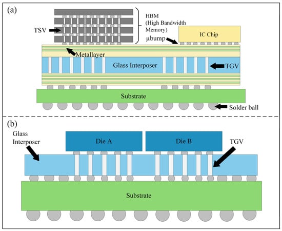
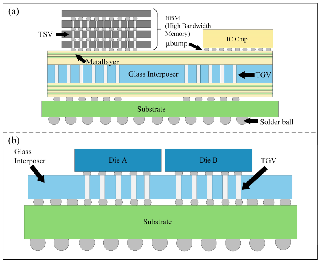
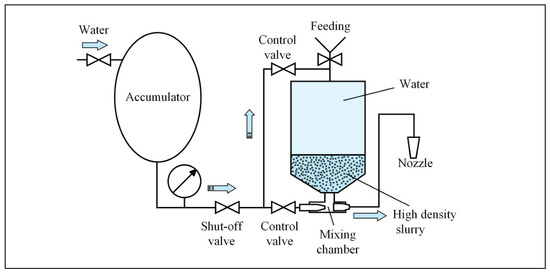
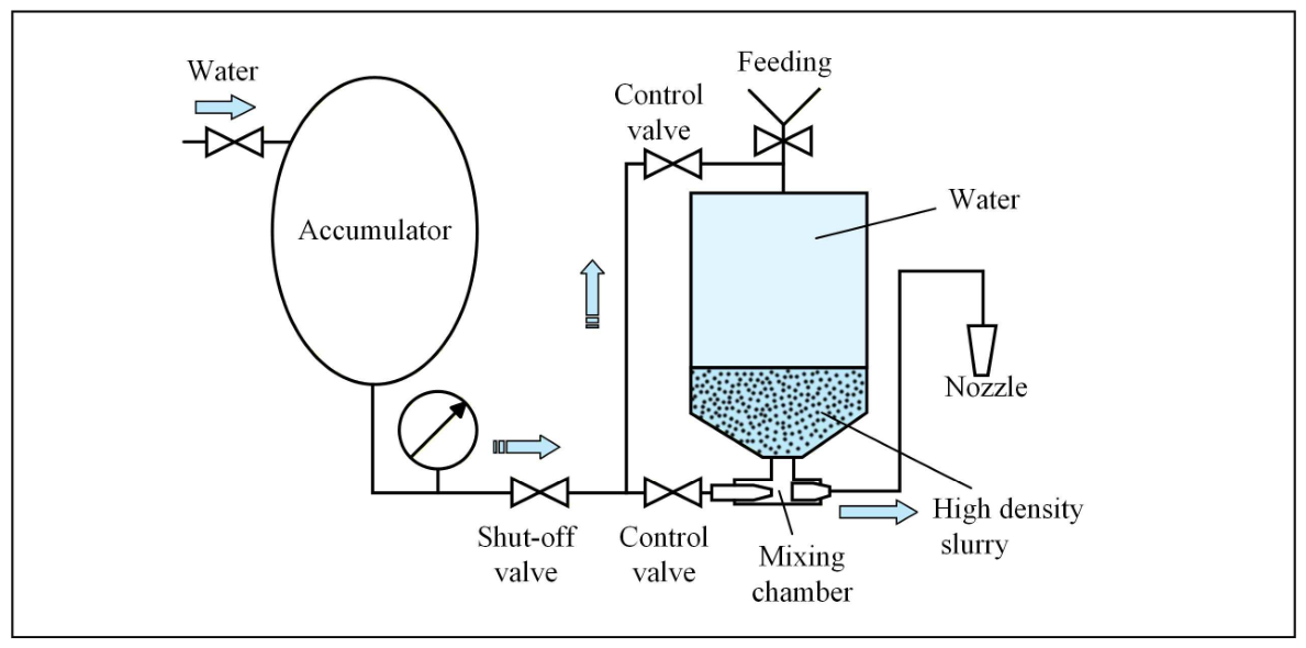
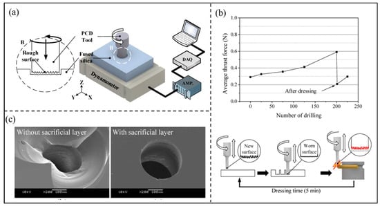
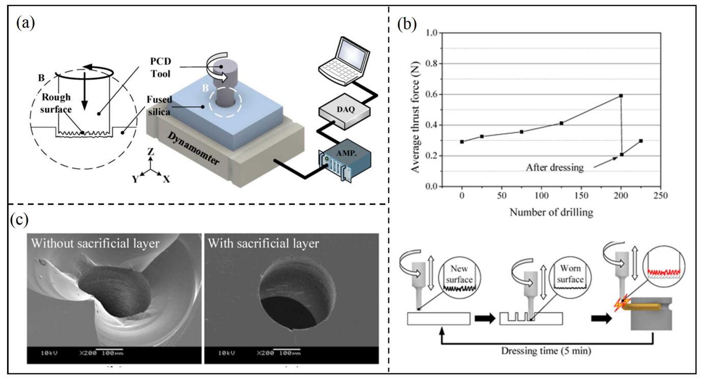
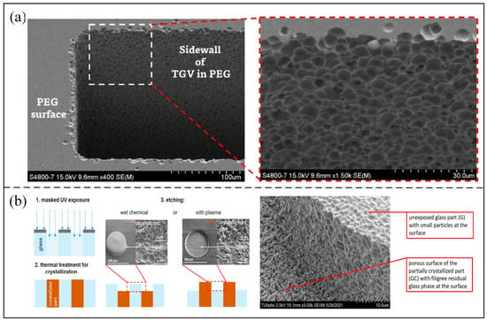
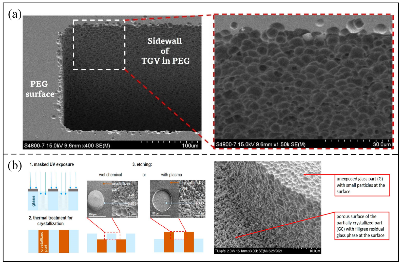
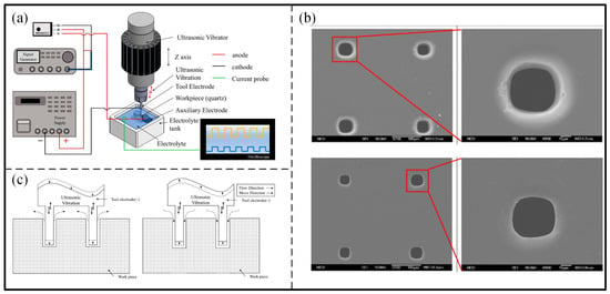
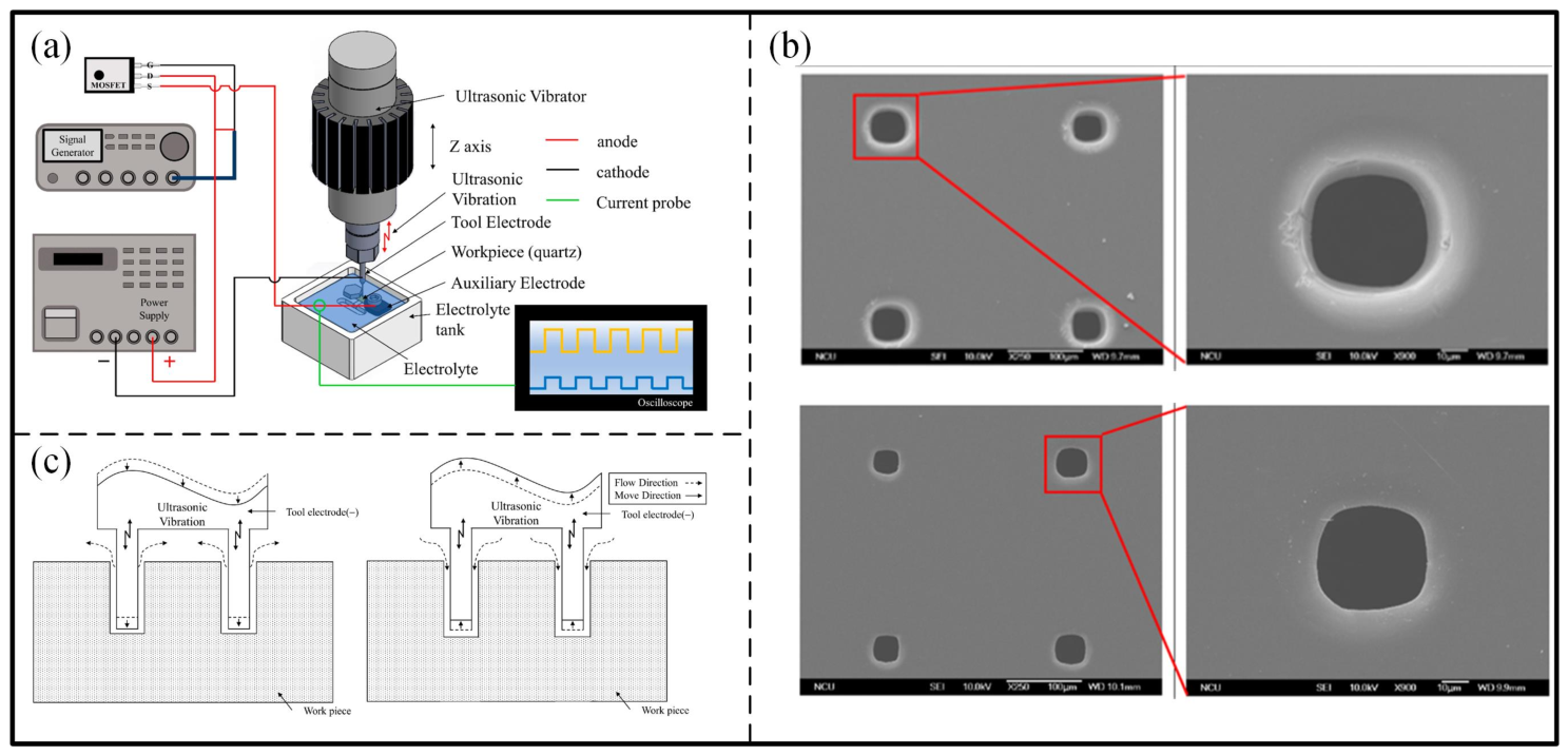
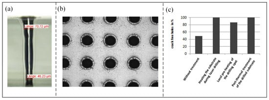
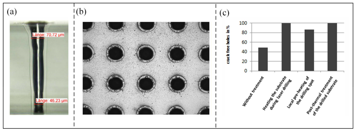
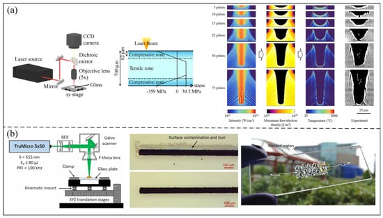
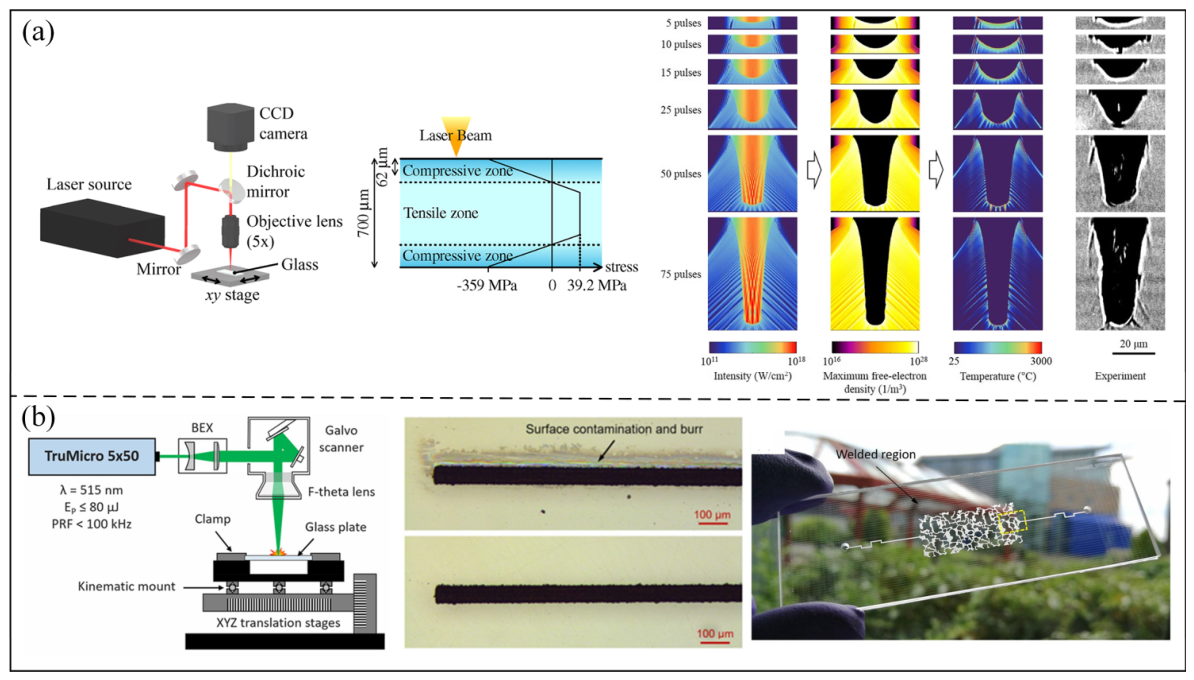
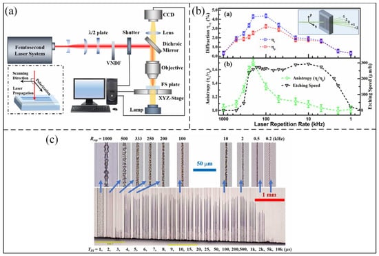
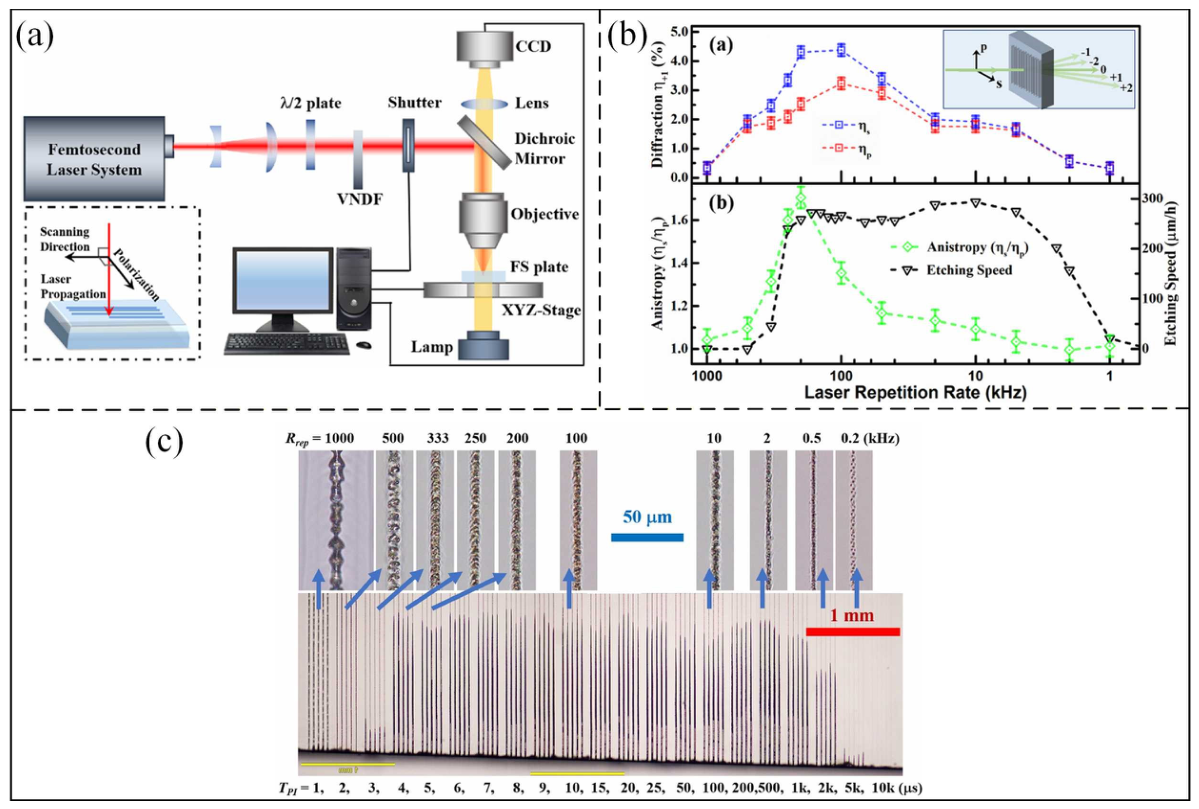
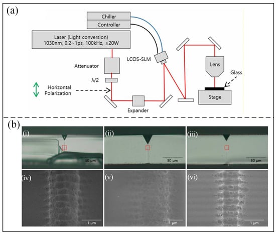
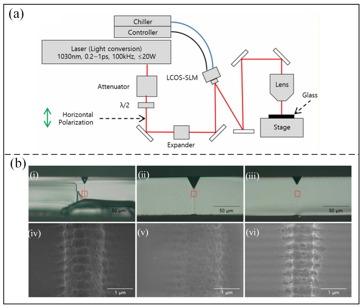
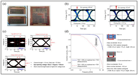
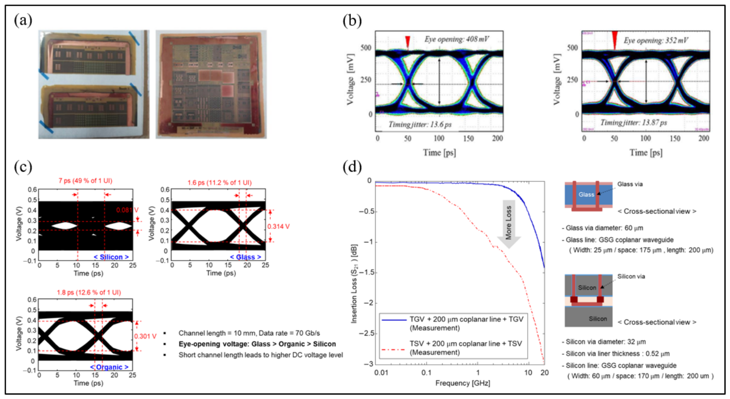
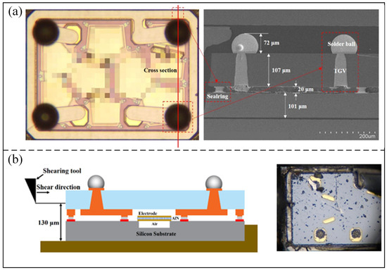
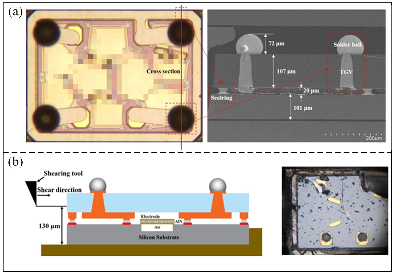
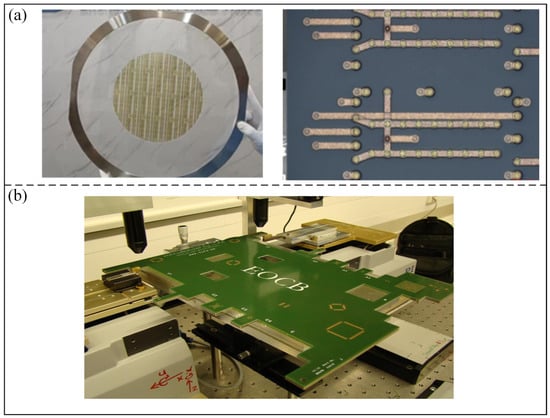
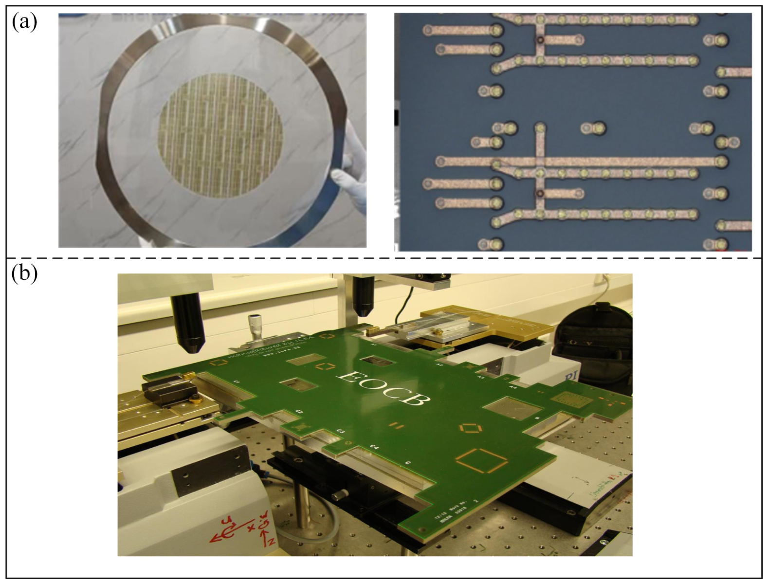

Disclaimer/Publisher’s Note: The statements, opinions and data contained in all publications are solely those of the individual author(s) and contributor(s) and not of MDPI and/or the editor(s). MDPI and/or the editor(s) disclaim responsibility for any injury to people or property resulting from any ideas, methods, instructions or products referred to in the content. |
© 2026 by the authors. Licensee MDPI, Basel, Switzerland. This article is an open access article distributed under the terms and conditions of the Creative Commons Attribution (CC BY) license.