1. Introduction
As telecommunications increasingly dominate various sectors, researchers worldwide—especially over the last decade—have focused on developing devices that meet the diverse requirements and standards set by international organizations. These requirements include the allocation of frequency ranges for telecommunication systems, high data speeds, and the rapid processing of information transmitted between transmitters and receivers. To address these demands, components have been developed to operate at very high frequencies, typically in the range of tens of gigahertz, particularly in the millimeter-wave spectrum. Efficient use of the frequency spectrum for data transmission has become essential. This has led to significant advancements in mobile communication technologies, culminating in the introduction of the fifth-generation (5G) networks [
1]. Like any wireless transmission system, 5G requires high-frequency ranges to support increased bandwidth. This includes both the sub-6 GHz frequency range and millimeter-wave bands, such as 26, 28, 38, and 60 GHz, enabling data transmission speeds of up to 20 gigabits per second [
2,
3]. In most electronic systems, essential components like filters play a critical role in separating unwanted signals from those required for specific applications. A bandpass filter allows signals within a specific frequency range to pass through while attenuating signals outside that range. These devices are widely used in the radio frequency (RF) domain and are based on various techniques, including substrate integrated waveguide (SIW) technology, a promising candidate for future advanced telecommunications circuits, where waveguides with a periodic structure can be used as RF devices in various applications [
4]. SIW is a modern form of transmission line that has gained popularity due to its efficiency in designing circuits operating in the radio, microwave, and millimeter-wave frequency spectrum. An SIW consists of a thin dielectric substrate, with metallic layers covering both the top and bottom surfaces [
5,
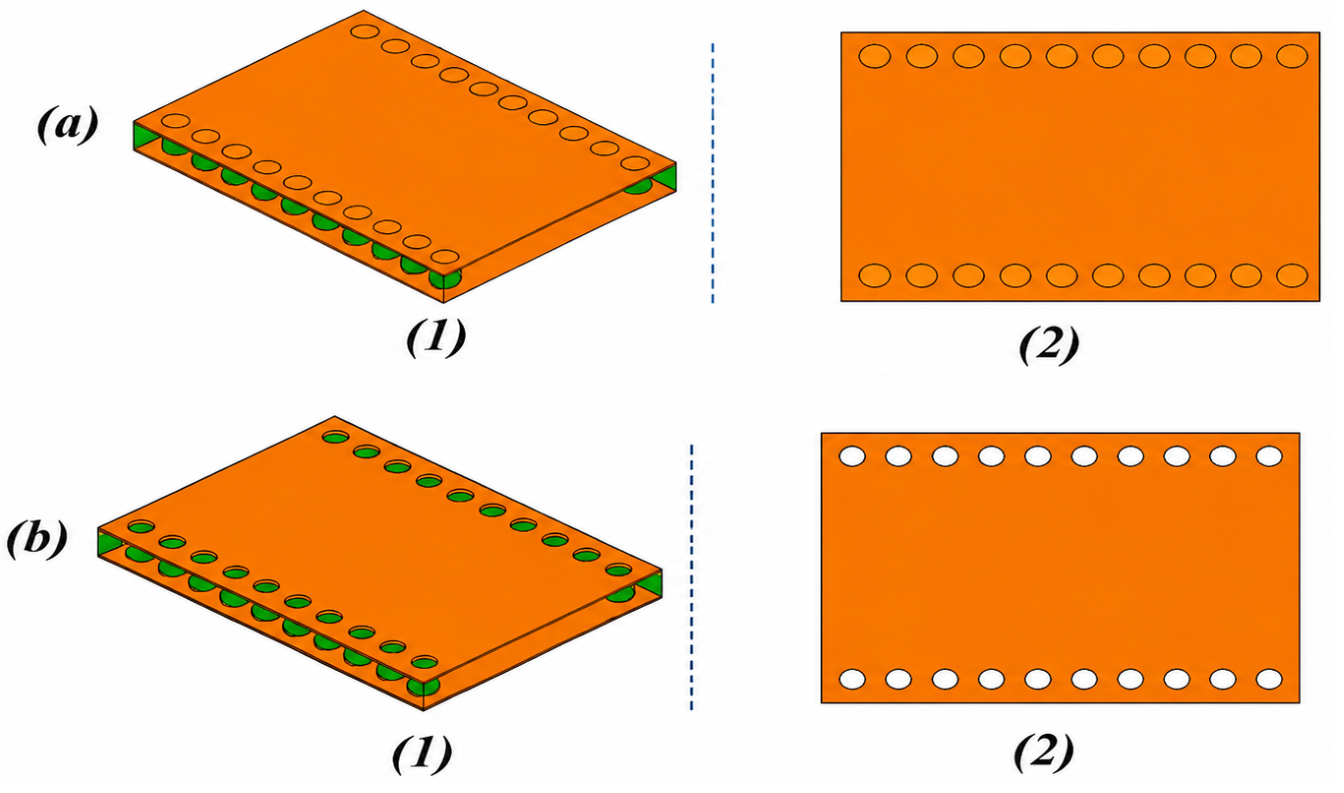
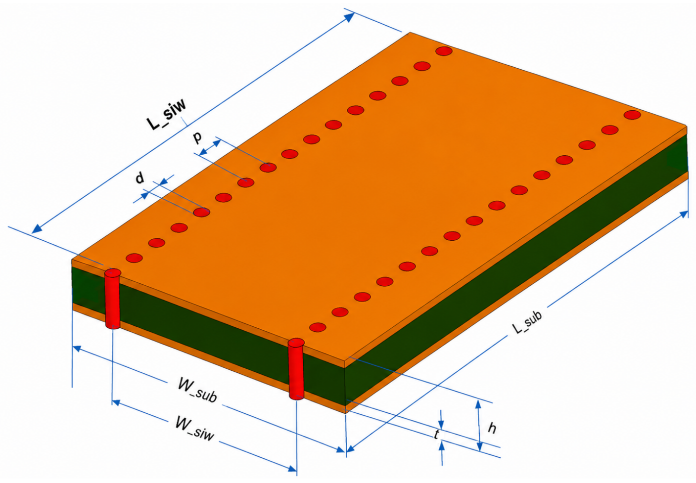
6]. The substrate contains two parallel rows of metallic via that define the wave propagation area; these via can be empty or full, as illustrated in
Figure 1a,b, which represent isometric and top/bottom view, respectively [
6].
Researchers have utilized various techniques to realize RF filters. One approach combines single-mode and dual-mode substrate-integrated waveguides (CSMDMSIW) [
7]. Another involves designing a wideband grounded coplanar waveguide (GCPW)-to-SIW transition [
8]. Some works propose a novel class of compact dual-mode bandpass filters based on half-mode substrate-integrated waveguide (HMSIW) cavities [
9], or filters with ultra-wide stopbands using multi-stub-loaded resonators (MSLRs) [
10]. Other designs use coupled line resonators (CLR) [
11]. Several researchers have proposed ultra-wideband (UWB) bandpass filters with stopband characteristics using a multi-mode resonator (MMR) technique [
12,
13]. A notable contribution involves a novel class of dual-mode SIW bandpass filters that exploit perturbed SIW rectangular cavities (PSIWRCs) [
14]. Additional filters are based on electromagnetic coupling of twin square metamaterial resonators (SRRs) and complementary split-ring resonators (CSRRs) [
15]. Other designs include dual-band bandpass filters inspired by a pair of square coupled, interlinked, asymmetric tapered metamaterial resonators [
16], when a dual-band filter is a type of electronic filter capable of selectively passing or attenuating signals in two distinct frequency ranges, often with a transition band between them. These filters are crucial in fields such as telecommunications and signal processing, where separating or combining signals at specific frequencies is essential, achieving high selectivity through quadruple-mode, multi-stub-loaded ring resonators (SLRRs) [
17]. While some approaches use non-resonant nodes (NRNs) based on single- and dual-mode cavities to form tri-layer stacked SIW structures (TLSSIW using NRN) [
18], others utilize multi-mode resonators (MMRs) [
19], or even machine learning methods to design compact UWB bandpass filters with notch characteristics using rectangular resonators [
20]. Finally, some works propose and design wideband fifth-order bandpass filters using U-slotted substrate-integrated waveguide (USSIW) cavities [
21].
In this work, a dual-band passband filter is proposed and designed using substrate integrated waveguide (SIW) technology. The study focuses on the theoretical design and electromagnetic simulation of the filter, while no physical fabrication or experimental manufacturing of the proposed structure has been performed. The proposed filter based on SIW technology operates in the millimeter-wave range, specifically within the Ka band, and resonates at two frequencies allocated for 5G applications: 28 GHz and 38 GHz [
5], where the 28 GHz band, corresponding to the 5G NR n257 standard, and the 38 GHz band, which falls within the 5G NR n260 frequency range, are widely recognized as key millimeter-wave bands for 5G communications, offering large bandwidths and supporting high-data-rate wireless services. This compact device demonstrates very good performance, achieving a return loss (RL) of around 44 dB, an insertion loss (IL) of 0.68 dB at 28 GHz, and an RL of around 53 dB, IL of 0.86 dB at the specified frequency of 38 GHz. The simulation of this design and its results are obtained using a high-frequency structure simulator, ANSYS HFSS 15.0, which can be referred to 3D electromagnetic (EM) simulation software to design and simulate high-frequency electronic products, such as antennas, antenna arrays, high-speed interconnects, connectors, IC packages, printed circuit boards, RF or microwave components, and, especially, filters. These results are subsequently validated by the CST Studio Suite 2019 software. Overall, the main contributions of this work are summarized as follows:
Design and simulation-based of a novel compact substrate-integrated waveguide (SIW) bandpass filter operating at two key 5G frequencies: 28 GHz and 38 GHz, with a small footprint of 10.81 mm × 6.23 mm.
Demonstration of high performance in the Ka-band with sharp skirt selectivity, low insertion loss (approximately 0.68 dB), and excellent return loss (approximately 43.63 dB at 28.05 GHz and 52.65 dB at 37.96 GHz).
Integration of a high-performance Rogers RT/Duroid® 5880 substrate, which is manufactured by Rogers Corporation in Chandler, AZ, USA, in order to reduce both physical dimensions and weight, making it suitable for 5G miniaturized components.
Implementation of a simplified second-order Butterworth equivalent circuit model that facilitates easy fabrication and practical integration into 5G communication systems.
Compared to related works, the proposed approach provides a simplified structure with a reproducible design methodology while maintaining competitive filtering performance in both passbands.
2. Theoretical Analysis
The substrate integrated waveguide (SIW) filter proposed in this paper is designed using Rogers RT Duroid 5880, a high-frequency laminate material engineered specifically tailored for RF and microwave circuit applications. This substrate is particularly well suited for high-frequency analog and digital circuits operating up to millimeter-wave frequencies. Rogers RT Duroid 5880 is distinguished by its unique combination of low electrical loss and consistent mechanical performance. It features a low-loss tangent (tan
δ = 0.0009) and an exceptionally low dielectric constant (
= 2.2) at frequencies above 10 GHz. With a thickness of 0.508 mm, it supports stable signal propagation with minimal attenuation, making it ideal for high-performance RF components [
13,
19]. The dimensions of the substrate are essential for the accurate design of the SIW filter, such as the substrate length (
), width (
), diameter of the via (
d), and spacing between adjacent vias (
p). These dimensions are determined using established formulas [
5,
22]. These physical parameters, illustrated in
Figure 2, influence the filter’s performance, ensuring efficient transmission of electromagnetic waves within the desired frequency range [
22,
23].
2.1. General Case (Single Bandwidth)
The proposed filter was designed to operate at target frequencies of 28 and 38 GHz.
As the SIW is equivalent to a rectangular waveguide where
, the dominant propagation mode is
. The resonant frequency, which depends on the effective width
and effective length
of the waveguide, can be accurately calculated using the following formula [
2,
4,
7,
23]:
Here, the resonance frequency of the dominant mode is
. Therefore, the first lower cutoff frequency corresponds to the
mode, which can be calculated from Equation (
1) by choosing the mode indices
:
On the other hand, the upper cutoff frequency, which is
, is equal to
. In order to obtain a system without leaks, it must choose very suitable values of
d,
p,
, and
. The wavelength at the center resonant frequency of the SIW
must be found:
Otherwise,
must be greater than
to obtain a propagation in the system. This is inspired by the following formula for the guide wavelength:
Therefore, the second part of Equation (
4) must be positive, or
where
represents the wavelength at the cutoff frequency, and is generally equal to twice the effective width of the SIW (
). The width of the SIW (
), represented by the distance between the two walls of the vias, can be calculated through the following relation:
Here,
p and
d can be found in Equation (
7): [
5,
22,
23]
The total width of the SIW () must be greater than or equal to , and the same condition applies to the total length (), which must be bigger than or equal to , with the aim of minimizing the losses of the propagation. The insertion of symmetrical shunt spots with diameters equal to on the SIW cavity can transform it into a narrow bandpass filter. This device can be fed through a microstrip line that guarantees the transition from the quasi-TEM mode of the microstrip line to the mode of the waveguide.
Generally, an SIW structure without resonators in the middle functions as a traditional waveguide. However, the addition of resonators, such as irises or spots, within the SIW can transform it into a passband filter (PBF) or stopband filter (SBF) [
24].
2.2. Special Case (Dual Bandwidth)
To design a filter that resonates at two frequencies, each corresponding to a propagation mode, the first step is to start from the first lower cutoff frequency
, which is represented in Equation (
2), in order to find the effective width of the filter, and then determine the effective length according to the resonance frequency of the dominant mode
according to Equation (
1).
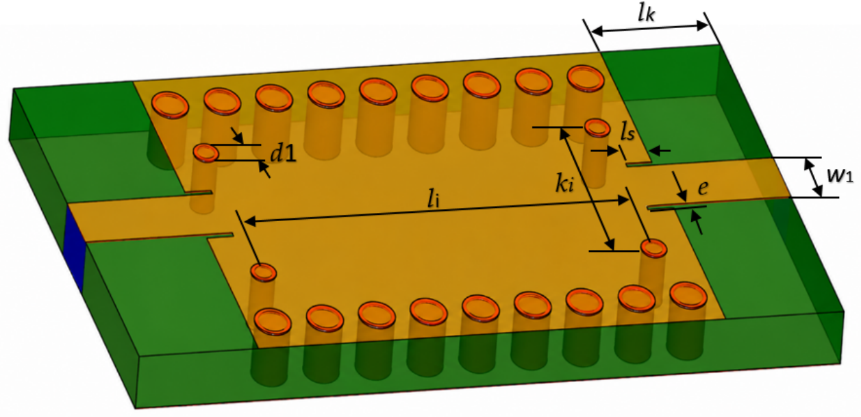
Subsequently, the insertion of resonators, positioned vertically apart by a distance
, and horizontally by
, in the form of shunts or spots with a diameter
, as shown in
Figure 3, enables resonance at two distinct frequencies. Achieving the desired resonance frequencies simply requires adjusting the dimensions
,
, and
accordingly [
24,
25].
2.3. Design of the Proposed Filter
As the proposed filter observed in
Figure 3 operates at both bandwidths centered around the working frequencies 28 and 38 GHz, the first cutoff frequency must be lower than 28 GHz; and to cover the entire desired bandwidth,
must be at least 24 GHz with
. For this and according Equations (
1) and (
2), we obtain
It is implied that
; therefore,
according to Equation (
7). In addition,
can be approximately 7.22 mm for the central resonance frequency of 28 GHz, and 5.32 mm for 38 GHz. Thus,
at 28 GHz and 6.87 mm at 38 GHz according to Equation (
4). As the dimensions of the substrate do not change after fixing its length and width to obtain a resonant frequency at 28 GHz for the dominant mode
, then, in order to obtain another resonant frequency at 38 GHz in the second mode
, it is necessary to control the appropriate dimensions and positions of the resonators placed inside the filter, especially
,
, and their diameter
.
Based on all the equations mentioned above, all the dimensions or parameters of the proposed filter shown in
Figure 3 can be calculated, while those not mentioned in this figure are the same as those shown in
Figure 2.
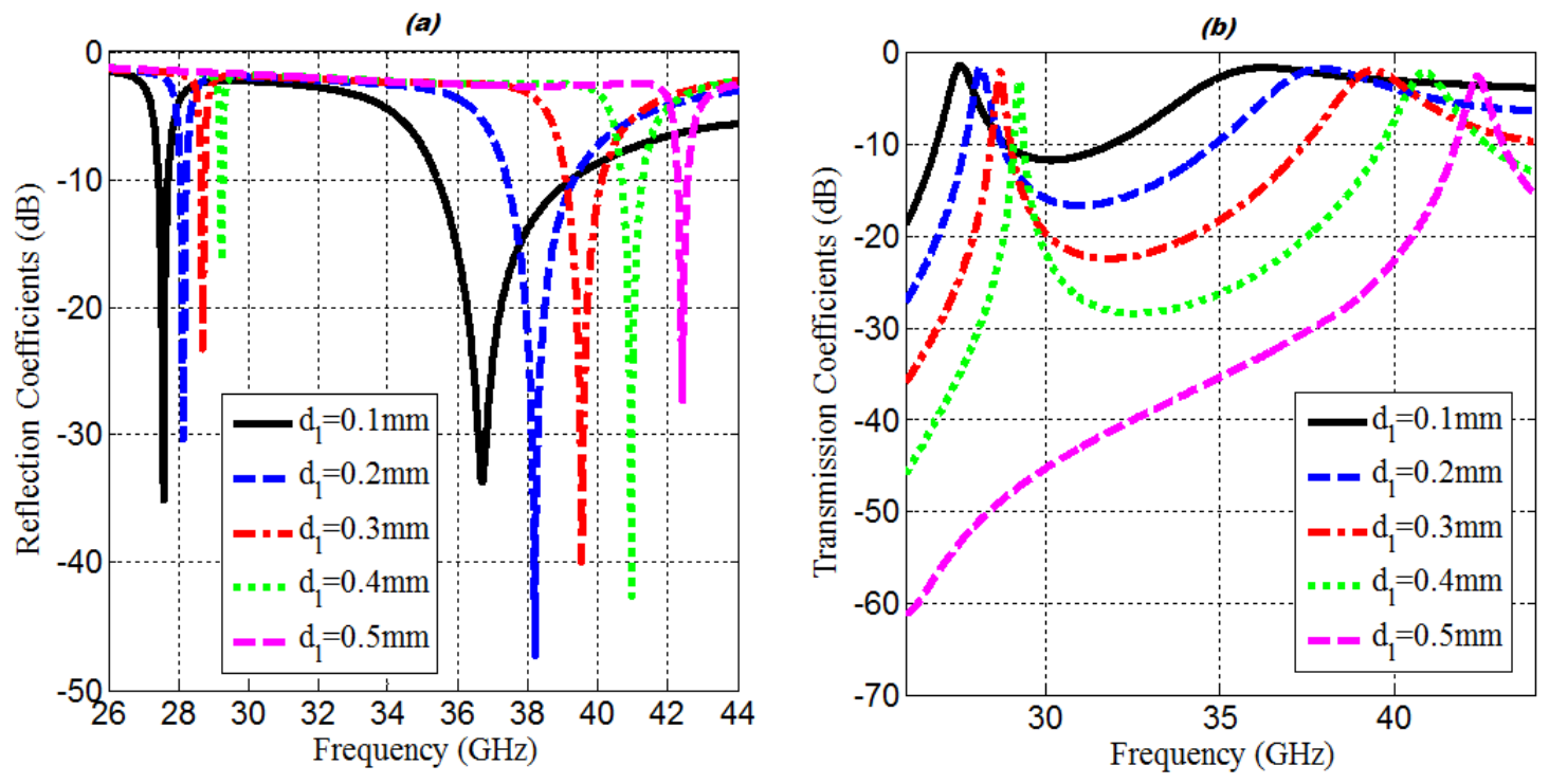
The proposed filter is embedded or loaded with resonators in the middle in the form of shunts or cylindrical irises of identical diameters to simplify the calculations; the positioning of these resonators plays a very important role in determining the resonance frequencies [
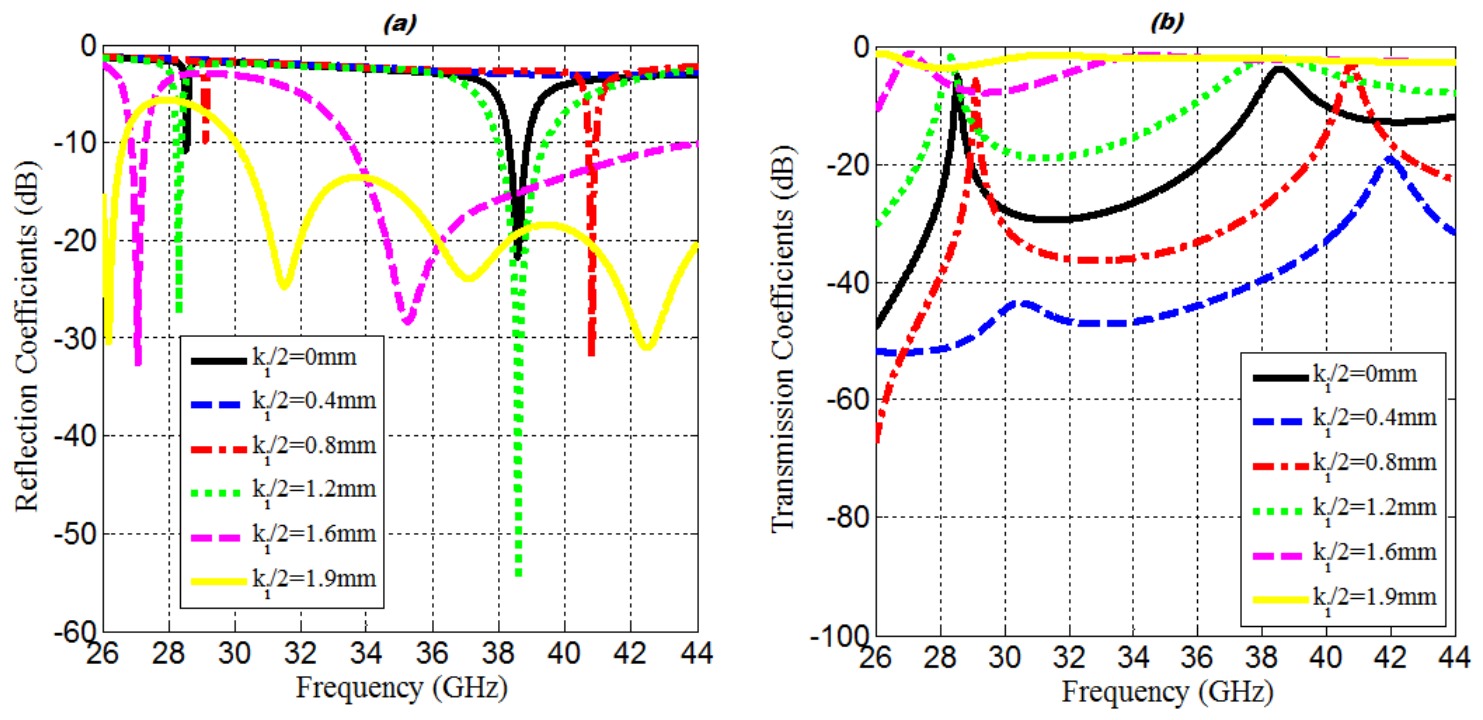
24]. As shown in
Figure 4b and
Figure 5b, which illustrate the variation of the transmission coefficient
in dB or IL, the gap between the two passbands decreases or increases depending on the variations of the parameters
and
. This variation also affects the reflection coefficient
in dB or RL, which can reach a value of 54.69 dB at a resonance frequency of 38.59 GHz for a
value of 2.4 mm. On the other hand, an IL value of 52.9 dB is observed at a frequency of approximately 29 GHz for an
value of 2.6 mm according to what is shown in Part A. In contrast, the impact of the diameters of the resonators on the resonant frequencies and the bandwidth is direct and very clear, as seen in
Figure 6 and
Figure 7. It is, therefore, clear that the creation of the two bands is ensured by adjusting the distances between the resonators as well as their diameters.
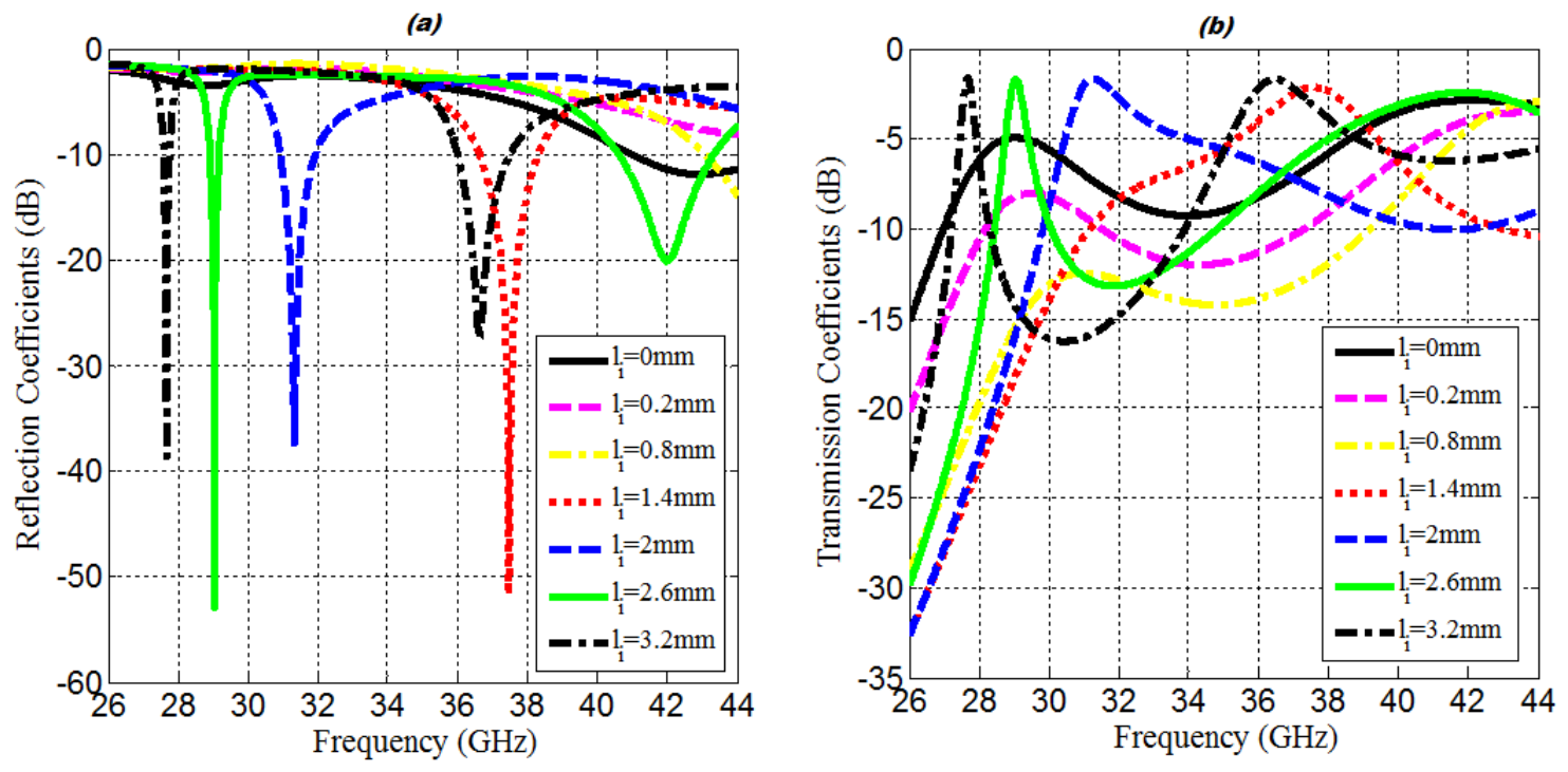
This filter is fed by a microstrip line with a length of
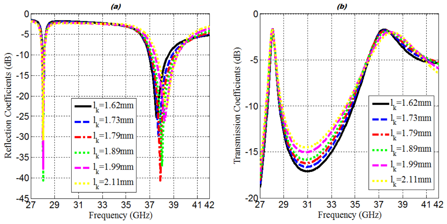
, which can influence its response. This effect is particularly noticeable on the second bandwidth, centered at 38 GHz, as illustrated in
Figure 7. It clearly shows the change in the frequency of the second bandwidth based on the increase or decrease in length
. This effect also affects
, where optimal values of return loss (RL) are observed: 35.98 dB at 38.02 GHz and 39.65 dB at 28.05 GHz for a value of
. However, this effect is not significant on the insertion loss (IL) represented by
in dB, as shown in
Figure 7b, except in the second bandwidth around 38 GHz.
3. Numerical Results
After determining the appropriate values for the dimensions of the filter, as illustrated in
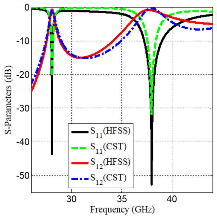
Table 1, we proposed and simulated the design using the EM software, specifically ANSYS HFSS 15.0. We then validated these results using another software, the CST Studio Suite 2019, to confirm their accuracy. It is clearly observed that the curves of the S-parameters in decibels, representing insertion loss (IL) and return loss (RL), are nearly identical, particularly at the resonance frequency of 28 GHz. However, the second passband centered at 38 GHz is noticeably wider in the HFSS simulation, extending up to about 3.6 GHz, compared to the CST simulation, where it is around 2.1 GHz.
The final S-parameters can be extracted and plotted as shown in
Figure 8, which represents the variation of the insertion loss and the return loss as a function of frequency based on the numerical parameters of
Figure 3. It is clearly noted that this device is characterized by two passbands: the first one around 28 GHz, which is a narrow band with high selectivity, and another one around 38 GHz, which is a wide band.
According to the HFSS simulation results, the first bandwidth ranges from 27.88 GHz to 28.26 GHz at , with a passband width of 380 MHz. The minimum insertion loss (IL) reaches 0.67 dB, and the maximum return loss (RL) is 43.63 dB at the first resonant frequency of 28 GHz. In addition, for the second band centered on the resonance frequency of 38 GHz, the bandwidth extends from 36.35 GHz to 40 GHz at , giving a width of 3650 MHz. The IL reaches its minimum value of 0.86 dB at 37.58 GHz and 0.96 dB at the resonant frequency of 38 GHz, where a high RL of 52.65 dB is observed at the exact frequency of 37.96 GHz.
For the CST simulation,
,
at 28 GHz, and
,
at 38 GHz. Therefore, the fractional bandwidth Δ (
FBW) and the quality factor
Q are defined as follows [
25]:
where
and
are the first and second −3 dB cutoff frequencies, such that
is the centered one. Therefore,
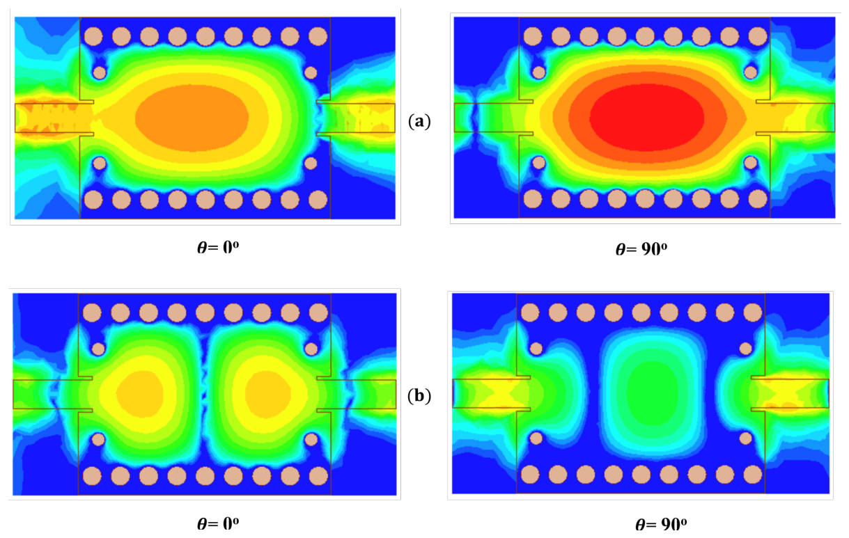
According to
Figure 9, which shows the electric field distribution on the SIW filter, we observe that the first resonance occurs at the
mode, with a polarization phase
equal to
rad, at the desired frequency of 28 GHz. On the other hand, the second resonance corresponds to the
mode, without phase shift, at the desired frequency of 38 GHz. It can be concluded that there is a 90-degree phase shift between the dominant modes
and
, corresponding to the resonance frequencies 28 and 38 GHz, respectively, whose electric field intensity takes its maximum value of the order of
(V/m) in the middle of the filter at the 28 GHz resonant frequency, of the
mode with a phase
equal to
, as shown in
Figure 9a, where it equals the minimum values of the order of
(V/m) for the same phase at the 38 GHz frequency of the
mode.
4. Equivalent Circuit Model
The proposed filter is introduced and investigated by the lumped-equivalent circuit (LEC) method, which is adopted to analyze the characteristics of the dual-band response based upon the low-frequency LEC [
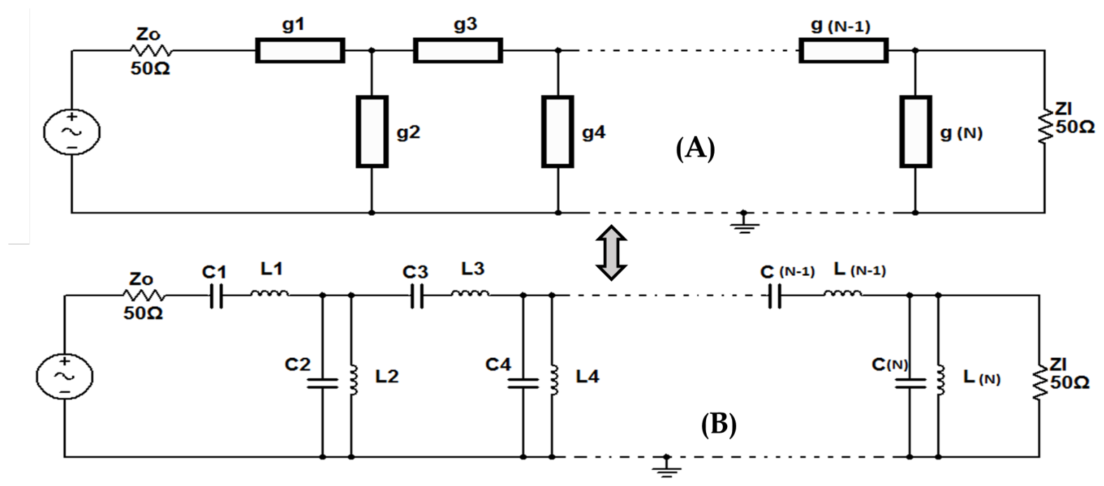
10]. This filter, designed using theoretical and analytical methods, can be considered equivalent to an electric circuit of Butterworth or Maximal flat type, based on the normalized low-passband filter (LPF) elements method “
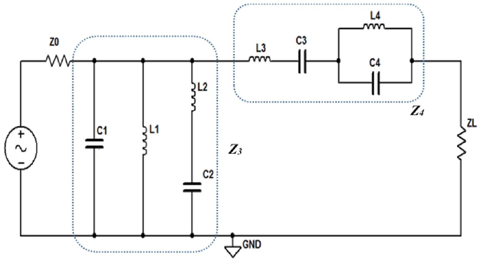
”, referring to Kuroda’ transformer, as shown in
Figure 10, where in our case, and in referring to the response of filter from the S-parameters shown in
Figure 8, it is clearly noted that this filter reacts as a Butterworth or maximally flat filter of order N with dual bandwidth [
2,
4,
26].
Generally, the
elements can be calculated from
And
N is the filter’s order, which calculated as
where
A is the insertion loss (IL) at the centered frequency
within the bandwidth, and
f is the lower first cutoff frequency. To transform the circuit as shown in
Figure 11 from (A) to (B), the following relationships must be used:
According to the previous formulas, it is important to note that they cannot be applied solely to single-band filters when determining equivalent circuits. In our case, the filter must be divided into two sections, each corresponding to one of the two bands. The first section will be centered around the 28 GHz frequency, while the second will focus on the 38 GHz frequency. Subsequently, we couple the two circuits to obtain the equivalent circuit for a dual-band filter. In addition, without delving into the complex calculations associated with Equation (
9), we can conclude that the filter is of second order, as it includes two pairs of resonators, making it a basic filter configuration.
4.1. First and Second Bandwidth Separately (Around 28 GHz and 38 GHz)
As mentioned above, and in order to determine the equivalent circuit of the proposed dual-band filter, as well as to be able to apply the previous equations, especially Equations (
9)–(
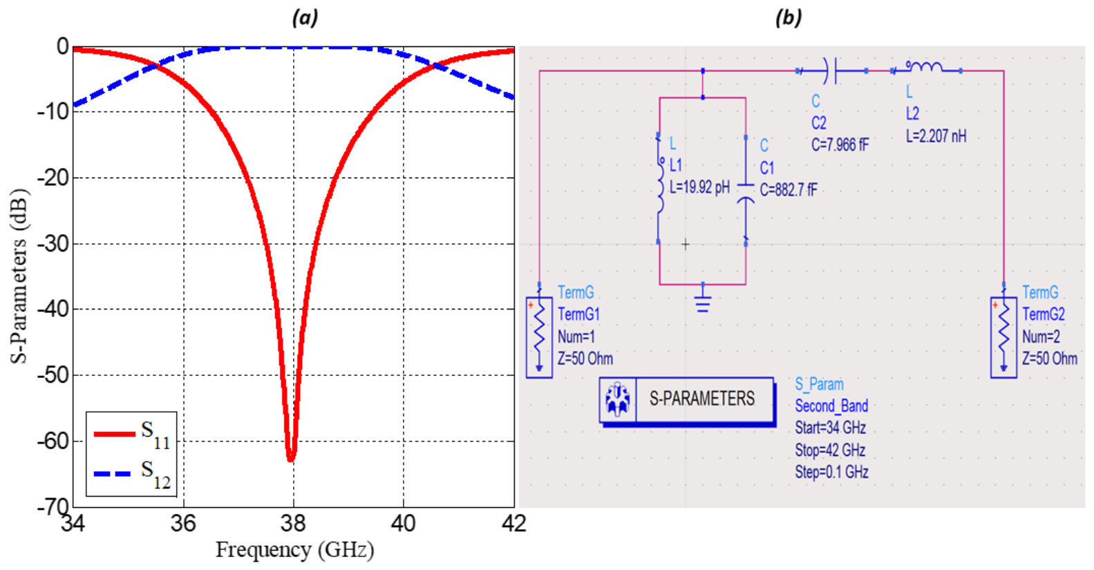
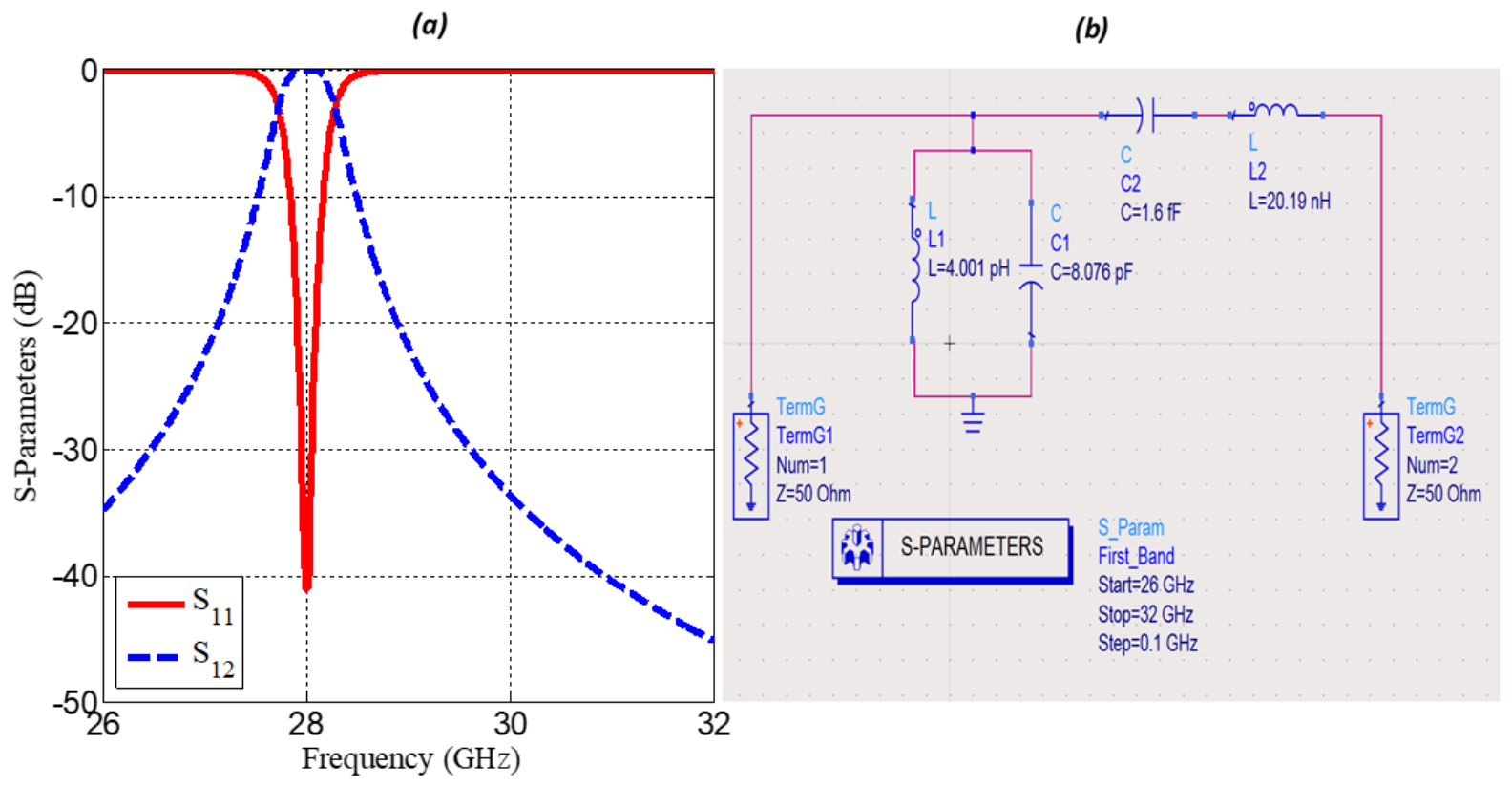
13), it is necessary to first find the equivalent circuit of each separate band, as shown in
Figure 11, because the SIW cavity can be described by an RLC equivalent resonant circuit [
27]. Then, it will be necessary to carry out the assembly and coupling of the circuits in order to determine the equivalent circuit of the final filter, in accordance with
Figure 12.
These two circuits were realized and simulated using Advanced Design System (ADS 2019) software; however, the value of each element for the first bandwidth is given in
Table 2, and for the second one is given in
Table 3, where the responses, represented as S-parameters, are plotted and extracted from the same software, as shown in
Figure 13 and
Figure 14, respectively.
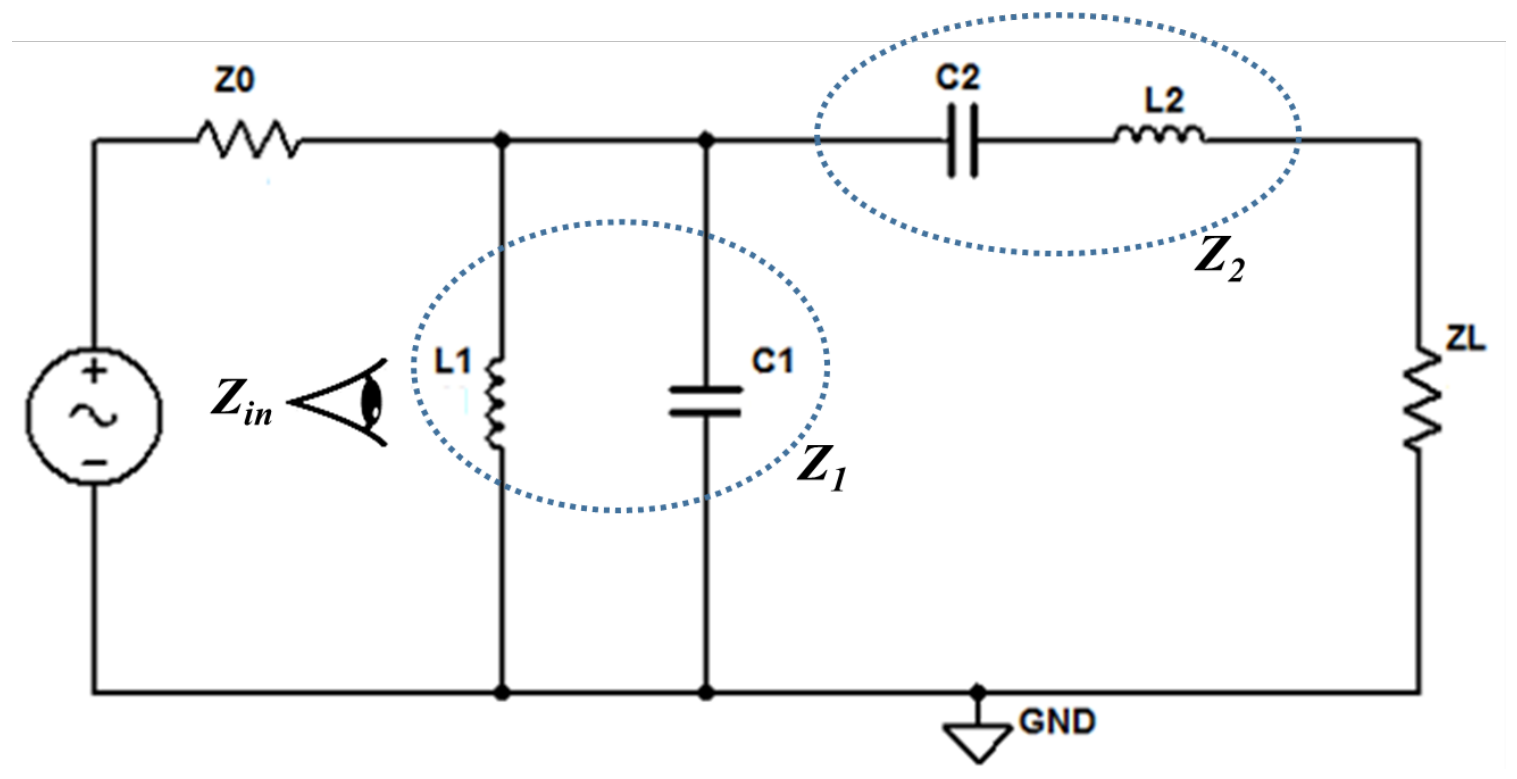
The resonance frequency of electronic filters can be represented by the following general formula:
We can approximate as that the resonance is dominated by the parallel branch
and adjusted by the series section
-
, as clearly observed in
Figure 11 and
Figure 12.
Therefore, for the parallel branch
,
And for the the series section
-
,
We can approximate also that the effective resonant frequency is the one where the total impedance seen by the source
is minimal, or where the phase of the denominator passes through zero (capacitive/inductive regime change). Here,
with
and
or
so
with
Ω.
4.2. Equivalent Circuit of the Proposed Filter
As mentioned before, it is not possible to directly apply the previous equations and the
elements method, as we have a dual bandwidth filter with two resonant frequencies
and
, as well as two fractional bandwidths
and
. For this, we rely on the circuit shown in
Figure 11 in order to realize the final equivalent circuit, as illustrated in
Figure 12.
The analysis is the same as the previous circuit, so the impedances
and
are responsible for achieving the resonant frequencies, 28 and 38 GHz, in the same design;
can be determined as follows:
with
The resonant frequency corresponds to when
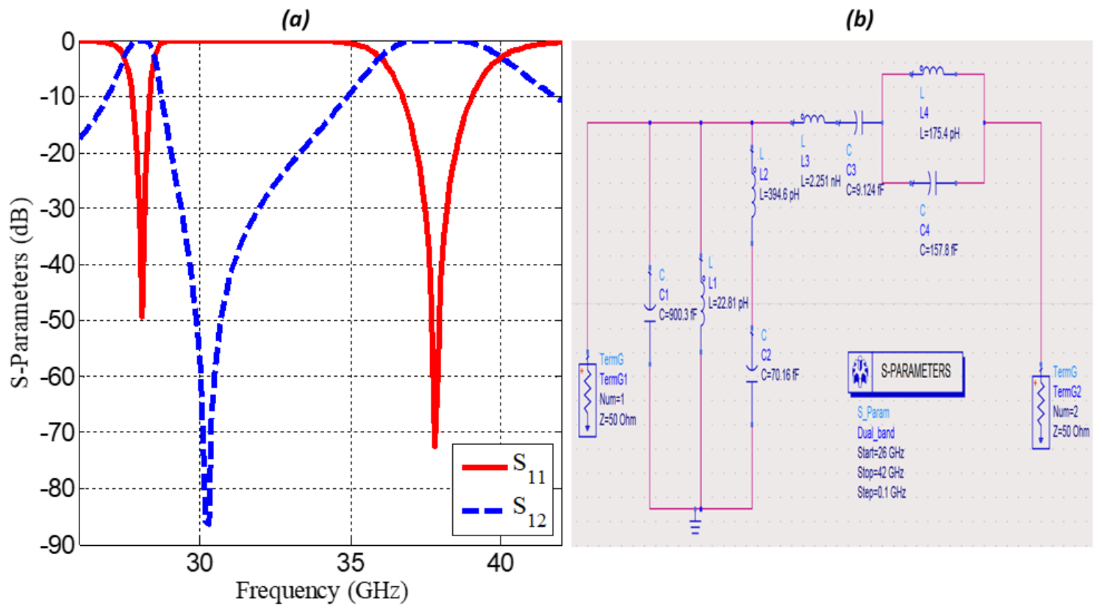
. As the theoretical calculations are quite complex, we opted to simulate and optimize the circuit using Advanced Design System (ADS). The component values used for the simulation are listed in the accompanying
Table 4, and the resulting response is illustrated in
Figure 15, as generated by ADS. In
Figure 12, the components
and
act as regulators or disruptors within the circuit, influencing the resonant frequencies while also facilitating coupling by forming a bandpass filter. This configuration enables the creation of a circuit with two distinct bandwidths. As previously discussed, we combined two earlier circuits and introduced coupling through branch 4. This configuration inherently generated a transmission zero (TZ) at around 30.3 GHz, thereby forming a band-stop filter that returns the signal to zero at this frequency, as shown in
Figure 15. To accurately identify the resonant frequencies, it is recommended to compute the transfer function of the overall circuit and determine the frequencies at which its argument becomes zero. An effective method to determine the resonant frequencies is through the calculation of the circuit’s transfer function,
. By analyzing this function, one can derive the system’s poles and zeros, which directly correspond to the resonant frequencies. The transfer function, typically expressed as the ratio of output to input voltage (or current), is
It serves as a fundamental tool in characterizing the frequency response of the circuit, where the amplitude-squared transfer function for Butterworth filters that have an insertion loss IL ≈ 3 dB at the cutoff frequency
, is given by
where
N is the degree or the order of filter, which corresponds to the number of reactive elements required in the lowpass prototype filter [
2,
4]. The resonant frequency corresponds to the value of
for which
is maximum, so
or
and
is the resonant frequency.
To assess the coherence between the S-parameter simulations obtained using HFSS and CST (as shown in
Figure 8) and those derived from the equivalent circuit modeled in ADS (illustrated in
Figure 15), we compare key filter parameters such as the resonant frequencies, insertion loss (transmission coefficient S12), return loss (or reflection coefficient S11), and the bandwidth of the passband. A strong correlation is observed between the results predicted by the equivalent circuit model in ADS and those obtained from full-wave electromagnetic (EM) simulations. While the overall agreement is substantial, minor discrepancies are noticeable. For example, the bandwidth of the first bandpass filter appears slightly wider in the ADS simulation compared to the EM simulations. Furthermore, RL and IL exhibit ideal behavior at the resonant frequencies, as summarized in
Table 5. Classical circuit theories, such as Ohm’s and Kirchhoff’s laws, are valid for low-frequency applications where circuit dimensions are much smaller than the operating wavelength. But in high-frequency domains, where wavelengths can be on the order of a few millimeters and become comparable to or smaller than the circuit dimensions, even a slight variation in the circuit geometry (ΔL) can significantly affect its behavior due to the presence of distributed effects.
5. Comparative Study
The performance of the proposed dual-band passband filter is compared with other reported filters in
Table 6. The developed filter is compact and has a good −3 dB FBW compared to most of the works. This work targets high-frequency mmWave (28–38 GHz), whereas all other references operate below 16 GHz except [
5,
8], which resonate in the Ka band. The proposed filter achieves exceptional return loss (RL) (43–52 dB), the best among all, and its insertion loss (IL) is moderate (0.7–0.86 dB), and better than most, except [
5,
11,
19], which are extremely low. Otherwise, the FBW is modest (1.36–9.61%), and not as wide as [
11,
12,
13,
21] which are designed with different techniques, as mentioned in
Table 6. However, this is expected for higher-frequency SIW designs. As for size, it is relatively compact for the operation of mmWave, and of a very small size compared to others (6.23 mm × 10.81 mm). As represented in
Table 6, the size is at the guided wavelength at a lower cutoff frequency
, so we cannot know the exact size in mm; on the other hand, [
19] is also compact, but for much lower frequencies.
Therefore, this work presents a high-performance mmWave bandpass filter with superior return loss, competitive insertion loss, reasonable compactness, and designed using SIW, which supports high-frequency integration.
6. Conclusions
In this work, a dual-band filter is proposed based on theoretical analysis and electromagnetic simulation results only, without physical fabrication or experimental validation, and designed without incorporating reconfigurability, which typically requires sensitive components, such as PIN diodes, that operate in the millimeter-wave range to achieve high frequencies in the tens of gigahertz range. The first band is a narrow band around 28 GHz, while the second one is a wider band around 38 GHz, both of which are designated for 5G applications. The device is designed using substrate integrated waveguide (SIW) technology, based on an inductive shunt iris with high performance, with a very high return loss (RL), having values of 40 dB and 50 dB at 28 GHz and 38 GHz, respectively.
The filter has a simple and compact geometric design, with overall dimensions of 10.81 mm in length and 6.23 mm in width (( × ) ≈ (3/2 × 1)/2), making it small and efficient. It has a planar structure with a thickness of 0.508 mm. Furthermore, it exhibits high selectivity at 28 GHz, characterized by a narrow band with a fractional bandwidth of −3 dB (FBW) of approximately 1.36%, and another wider band with FBW of approximately 9.61%. Consequently, the filter operates within the frequency ranges of approximately 27.84 GHz to 28.44 GHz and 34.91 GHz to 44.66 GHz.
Due to the existence of a simplified equivalent circuit for this filter, its design and fabrication demonstrate its feasibility for practical fabrication. Additionally, its compact size—with an overall length of 10.81 mm and a total width of approximately 6.23 mm—enhances its performance. The very small via diameter of 0.55 mm, the resonator diameter of 0.36 mm, and the thin substrate thickness of just 0.508 mm classify it as an extra-planar component. Furthermore, it exhibits dual resonance at two distinct frequencies—28 GHz and 38 GHz—using the same structure without requiring any modifications. These features make it an excellent candidate to serve as a key component in circuits and electronic devices operating in the millimeter-wave range and for next-generation communication systems and related technologies, especially in various 5G (fifth-generation) applications.



 ,
,