


Abstract
This work presents the design of a -Ga2O3 MOSFET incorporating a P-type Ga2O3 buffer layer on a high-thermal-conductivity AlN/SiC composite substrate. The electrical characteristics of the device were simulated using Sentaurus TCAD. Results demonstrate that the integration of the composite substrate effectively mitigates self-heating effects, reducing the peak temperature () from 776.5 K to 570.9 K at 300 K, while simultaneously increasing the threshold voltage () from −0.35 V to 1.52 V. Through systematic optimization of the P-Ga2O3 buffer layer thickness and doping concentration, the device achieves a breakdown voltage () of 4781 V, a power figure of merit (PFOM) of 2.18 GW/cm2, an , on/off ratio of 9.20 × 10⁹, and cut-off/maximum oscillation frequencies (/) of 1.29 GHz and 1.40 GHz, respectively. These findings provide a theoretical foundation for developing -Ga2O3-based power devices with high breakdown voltage, improved thermal conductivity, and low specific on-resistance ().
1. Introduction
-Ga2O3, as an emerging ultra-wide bandgap semiconductor material, possesses a wide bandgap of 4.8 eV, an extremely high critical breakdown field strength of 8 MV/cm, and a Baliga’s figure of merit (BFOM) of 3444 (·cm2)·V−2 [1,2]. It can be grown via the melt method, which enables low-cost crystal production and shows promising potential for applications in high-voltage, high-power, high-efficiency, and compact electronic devices [3,4,5,6,7]. Recent studies on the -Ga2O3 Metal-Oxide-Semiconductor Field-Effect Transistor (MOSFET) device have demonstrated breakdown voltages () exceeding 3 KV and a drain current () on/off ratio greater than 1010, positioning these devices as promising candidates for high-voltage and high-power electronic applications [8,9]. -Ga2O3 MOSFETs are classified into lateral and vertical configurations based on current transport orientation. Lateral -Ga2O3 MOSFETs are categorized into semi-insulating Ga2O3 substrate configurations, which employ Fe/Mg-doped p-type materials, and hetero-integrated substrates utilizing high-thermal-conductivity materials such as SiC and Si to enhance thermal performance [4,9,10,11,12,13,14,15,16,17,18,19,20,21,22,23,24,25,26,27]. However, the enhancement of device is typically realized by increasing drift region length or reducing drift region doping concentration, though these approaches inherently elevate the specific on-resistance (), thereby constraining device applicability in high-voltage high-power systems.
Vertical -Ga2O3 MOSFETs employing fin-shaped channels (FinFET) with top-side source electrodes and backside drain contacts achieve vertical current transport through drift regions with thickness decoupled from lateral dimensions [28,29]. This configuration enables electric field peak confinement within the bulk material through multi-gate structures while maintaining current pathways away from surface interfaces, thereby mitigating surface-state-induced reliability degradation and air-breakdown phenomena, which resolves the lateral device trade-off between conduction resistance and breakdown performance. In comparison with other wide-bandgap semiconductor materials, -Ga2O3 exhibits relatively low thermal conductivity (10–30 W/m·K) [3,4,30], which results in significant self-heating effects (SHEs) during high-power operation [31,32,33]. Elevated temperatures intensify lattice scattering (phonon scattering), reducing electron mobility and inducing current collapse in the device’s saturation region phenomenon termed the SHE. This SHE also restricts the device’s development and application in high-power and large-current fields [4,34,35].
The utilization of 4H-SiC substrates with thermal conductivity of 280 W/m·K (measured via laser flash analysis at 300 K) in -Ga2O3 devices significantly mitigates SHE [4,12,32,36]. However, the lattice mismatch between 4H-SiC and -Ga2O3 during heteroepitaxial growth, thereby degrading device electrical performance [5,37]. To address these challenges, p-type -Ga2O3 [11,38,39,40,41]/AlN/SiC heterostructure architecture is employed, where AlN serves as an epitaxial buffer layer due to its high thermal conductivity (260 W/m·K) and wide bandgap (6.2 eV) [42]. This combination enhances current drive capability by reducing interface scattering and improving heat dissipation [4,43]. The incorporation of P-type -Ga2O3 modulates electric field distribution in the channel region through hole-induced charge compensation, thereby enhancing the while simultaneously reducing the [43,44,45,46,47]. By optimizing the thickness and doping concentration of the p-type -Ga2O3 buffer layer and the 4H-SiC substrate, two enhanced device structures were finally designed, namely GaOPSiC1 with the best thermal conductivity and GaOPSiC2 with the highest breakdown characteristics. Compared with the existing reported device structures, they have significant advantages. The breakdown voltage can reach up to 4781 V, and the power quality factor is 2.18 GW/cm2. This device provides a theoretical basis for the development of high-voltage and high-thermal conductivity gallium oxide devices.
2. Device Structure
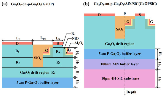
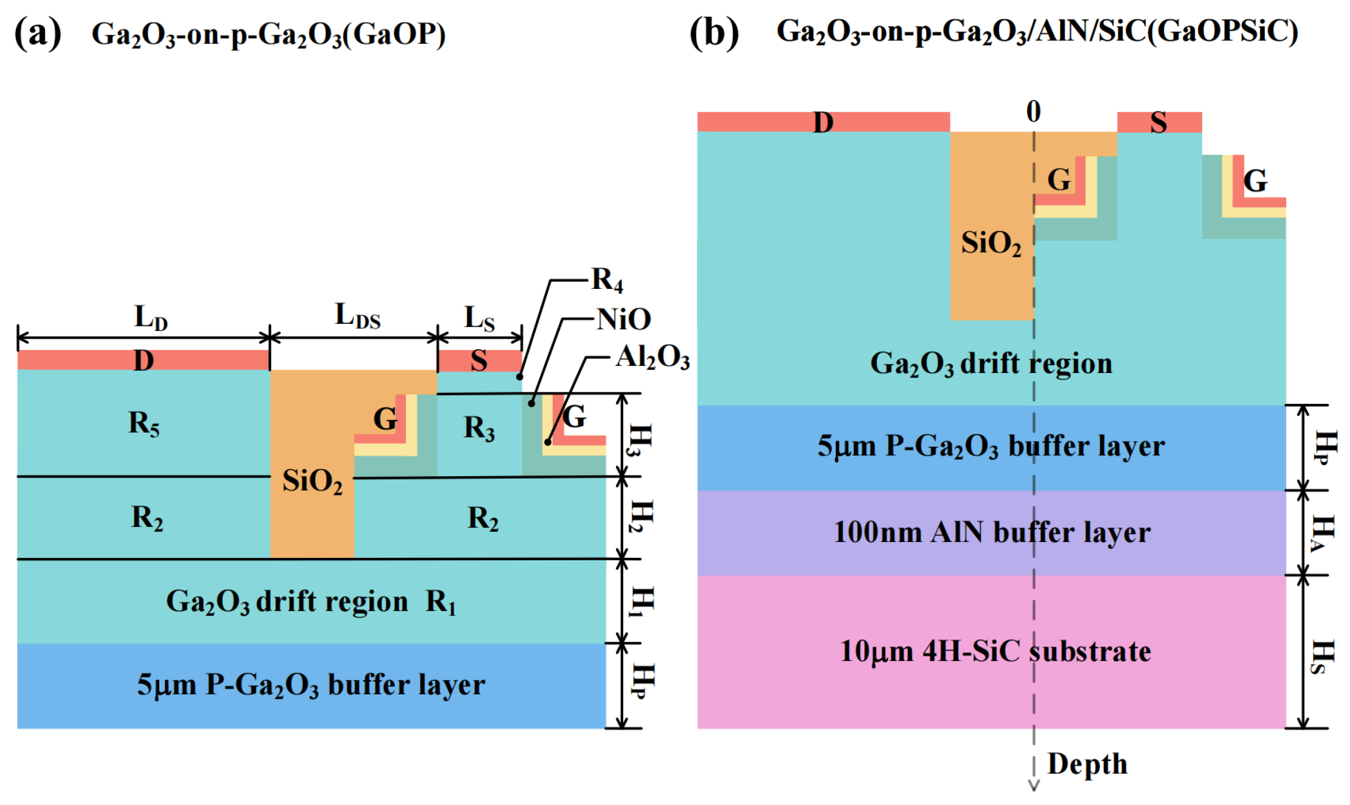
The device proposed in this study is depicted in Figure 1. Figure 1a presents the GaOP (-Ga2O3-on-P-Ga2O3) structure, which employs an iron or magnesium-doped p-type -Ga2O3 substrate with a doping concentration of = 2 × 10¹⁰–2 × 1020 cm−3 and thickness of = 1–10 μm [11,38,39]. Above the substrate, N-type -Ga2O3 drift region is positioned, which is partitioned into five segments labeled – with doping concentrations of – ( = = 1.45 × 1016 cm−3, = 2 × 1015 cm−3, = 5 × 1019 cm−3, = 2 × 1018 cm−3) and thicknesses of – ( = 4 μm, = 5 μm, = 0.80 μm, = 0.11 μm, = 0.91 μm). ( = 0.22 μm) and ( = 20.20 μm) are the source/drain electrode lengths. ( = 11 μm) defines the spacing between source and drain regions, with SiO2 as the isolation layer. The gate dielectric employs a composite structure of nickel oxide and Al2O3 to enhance gate modulation of the channel and suppress gate leakage current [22]. The nickel oxide layer is boron-doped with a concentration of 2 × 1017 cm−3, while the Al2O3 layer remains intrinsic. Their thicknesses are 0.1 μm and 0.03 μm, respectively. The gate electrode employs a platinum layer with a thickness of 0.03 μm, featuring a metal work function () of 6.30 eV. Figure 1b illustrates the GaOPSiC(-Ga2O3-on-P-Ga2O3/AlN/SiC) configuration. Compared to Figure 1a, the adoption of a P-type -Ga2O3/AlN/SiC composite substrate structure enhances the device’s thermal performance. The AlN buffer layer has a thickness of = 0.10 μm, while the 4H-SiC substrate exhibits a thickness of = 10–18 μm and a doping concentration of = 5 × 1013 cm−3. Except for the dimensions and doping concentrations marked in Figures 4–6, no other changes are made to the device.
Figure 1.
Schematic diagrams of (a) GaOP (b) GaOPSiC device structures.
The physical model is an indispensable part of the numerical solution process [48,49]. The physical models used in this paper mainly include the Bennett–Wilson model [50], which is employed to describe the energy band structure of semiconductors. The Philips unified mobility model proposed by Krishnaswamy [51] is used to illustrate the effects of temperature, lattice scattering, and electric field on mobility. The ionized impurity scattering Arora model [52] and the generation-combination SRH model [53] for describing the process of carriers exchanging between the conduction band and the valence band of impurities, and the avalanche breakdown Avalanche model [54] and the thermodynamic model [55] are used.
3. Results and Discussion
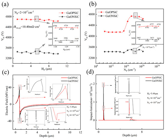
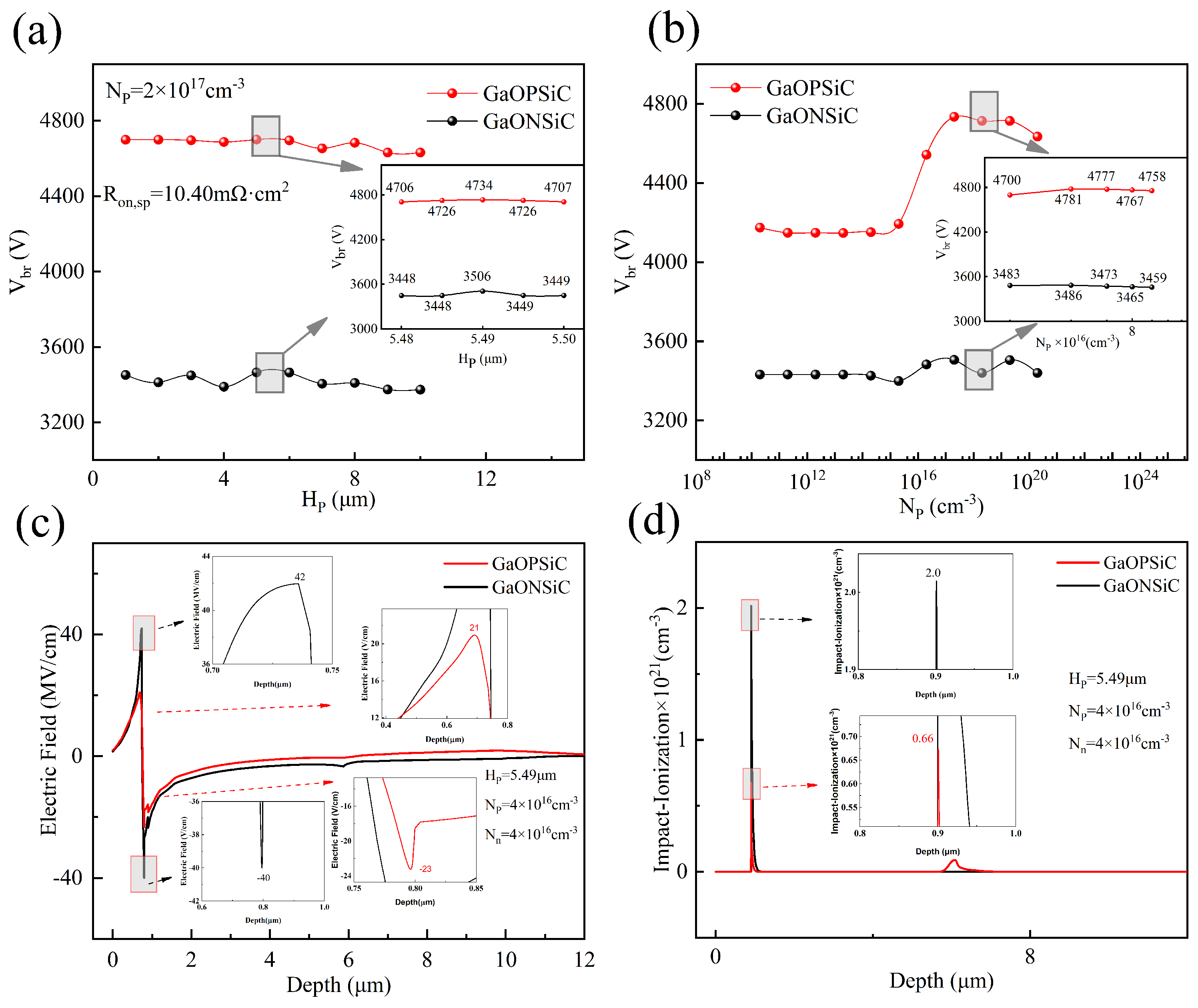
The simulation of this device was carried out using the TCAD software version of 2018. with the results documented in Figure 2, Figure 3, Figure 4, Figure 5, Figure 6 and Figure 7. Figure 2 presents a comparison of simulation results between GaONSiC and GaOPSiC structures designed on an N-type -Ga2O3/AlN/SiC substrate stack, where (a) illustrates the variation with at = 2 × 1017 cm−3, and (b) shows the dependence on at = 5.49 μm. Here, the breakdown voltage is defined as the value of the drain-source voltage when the drain current = 1 × 10⁻¹¹ A.
Figure 2.
Breakdown characteristic simulation results of GaOPSiC and GaONSiC devices. (a) variation with at = 2 × 1017 cm−3. (b) Breakdown voltage variation with at = 5.49 μm. (c) Electric field profile along the vertical depth beneath the left gate electrode. (d) Impact ionization rate distribution along vertical depth.
Figure 3.
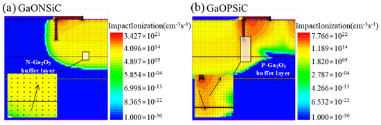
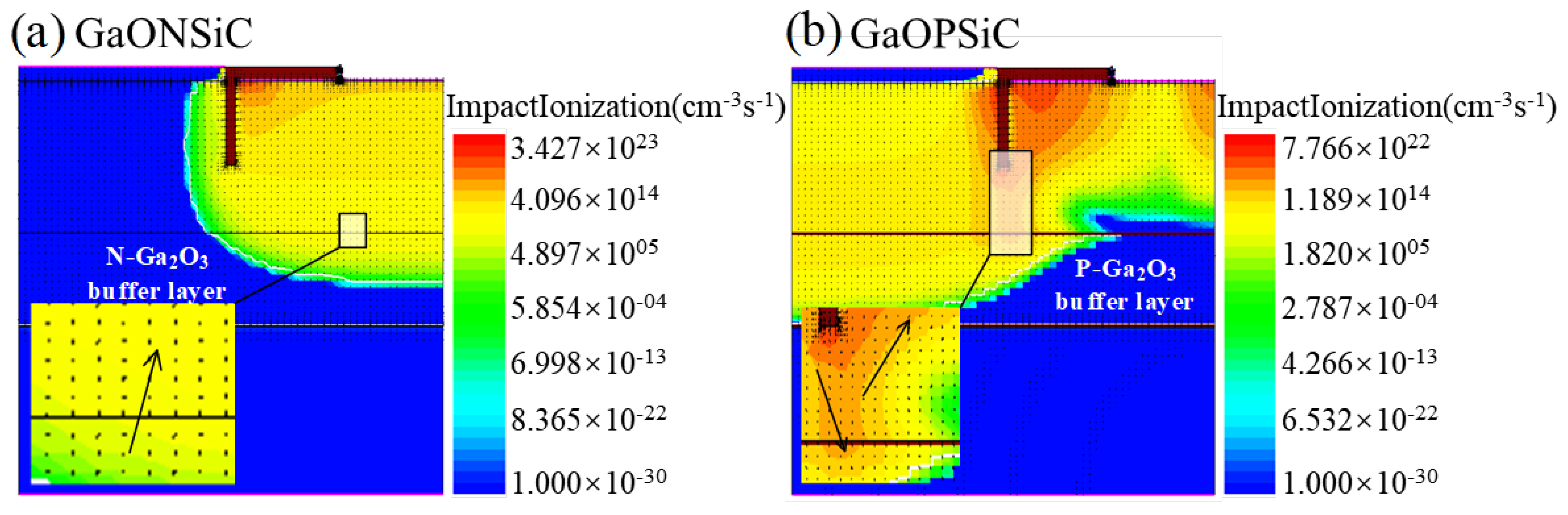
The distribution images of the internal electric field and the collision ionization rate during the GaONSiCand GaOPSiC device breakdown.
Figure 4.
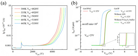
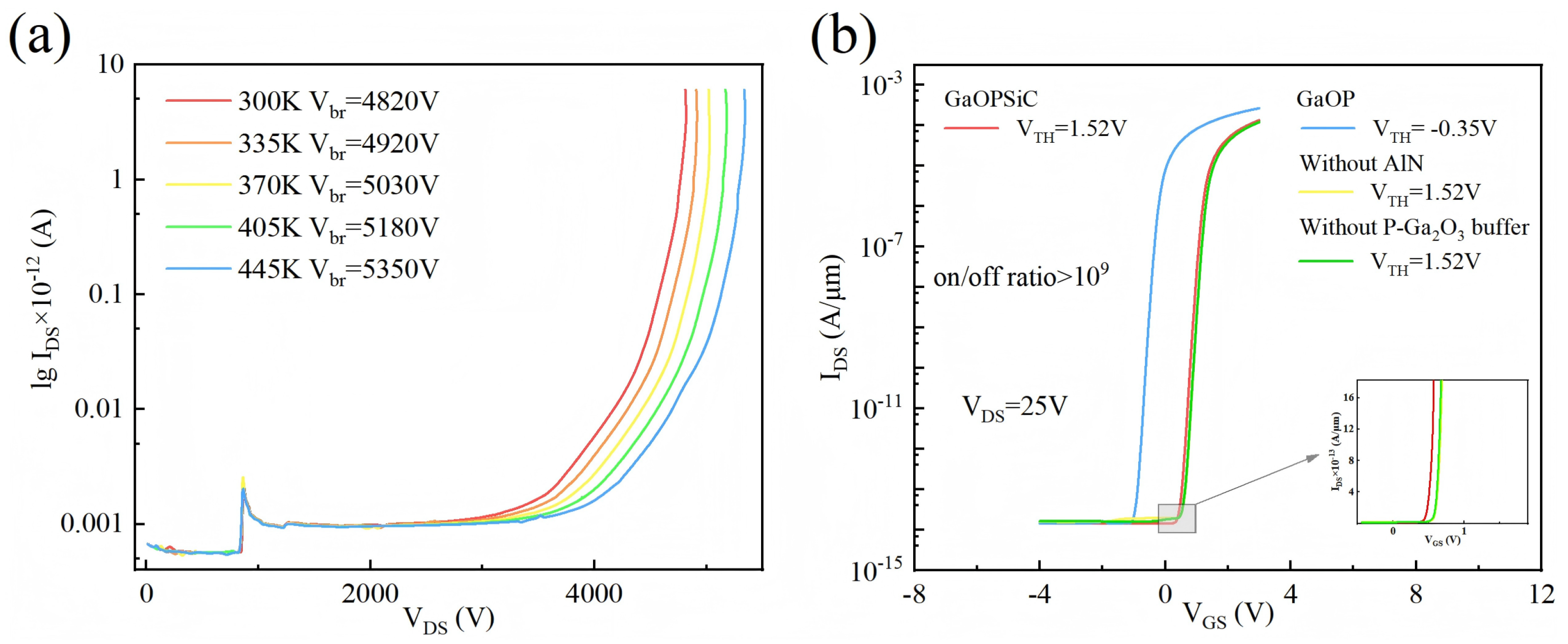
Device simulation results: (a) analysis - for GaOPSiC accounting for SHE at = 5.49 μm and = 2 × 1017 cm−3; (b) - in log scale of GaOPSiC, GaOP, without AlN, and without P-Ga2O3 buffer.
Figure 5.
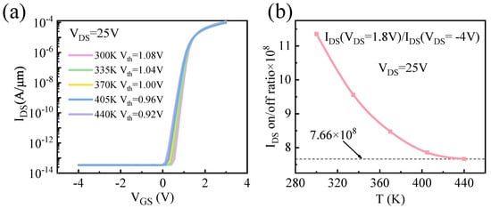
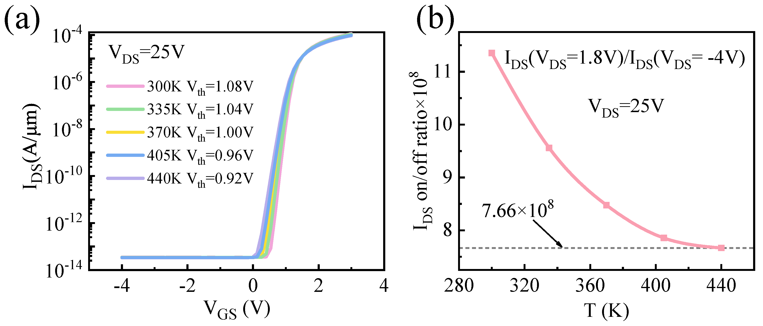
Simulation presents SHE in GaOPSiC with = 25 V: (a) - in log scale; (b) on/off ratio vs. T.
Figure 6.
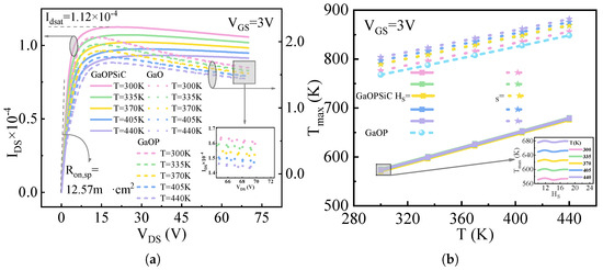
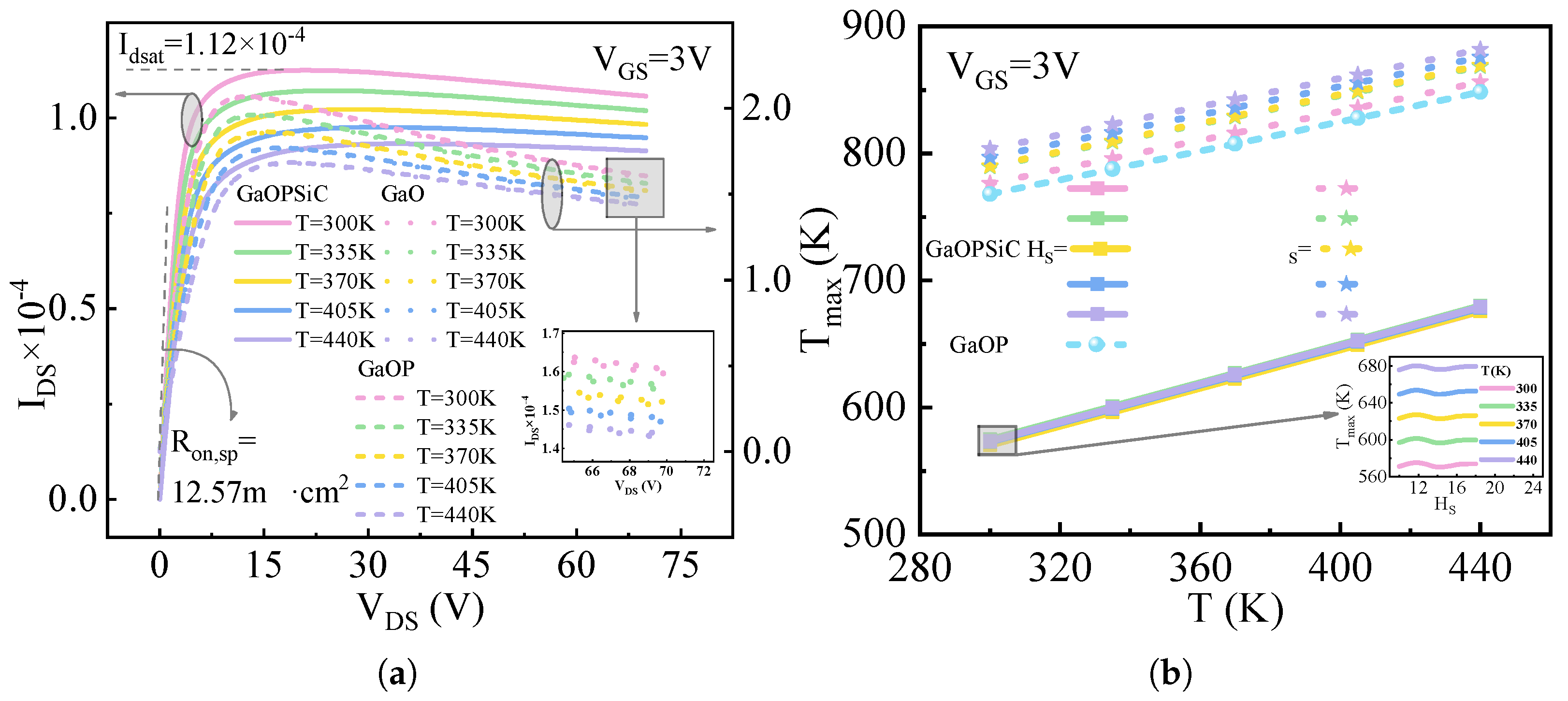
Simulation of self-heating effect in device: (a) - characteristics at = 3 V and = 10 μm; (b) vs. T for different at = 3 V.
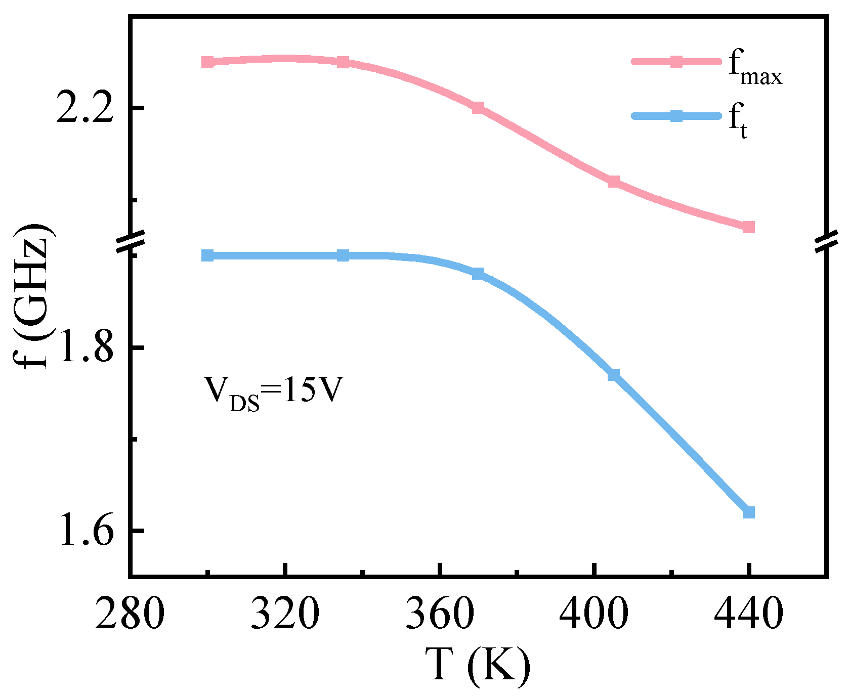
Figure 7.
f vs. T of GaOPSiC at = 15 V.
The simulation results demonstrate that GaOPSiC exhibits superior breakdown capability compared to GaONSiC, with GaOPSiC achieving record-high of 4781 V at an optimized doping concentration ( = 4 × 1016 cm−3) and structural thickness ( = 5.49 μm). This operational point corresponds to of 10.40 m·cm2 and an exceptional power figure of merit (PFOM) of 2.20 GW·cm−2, underscoring its potential for high-power applications. In comparison with the GaONSiC of identical dimensions, GaOPSiC presents 1295 V enhancement in , 0.55 m·cm2 reduction in , and 1.10 GW·cm−2 improvement in PFOM.
Figure 3 shows the distribution of electric field and collision ionization rate at various locations during the breakdown of GaOPSiC and GaONSiC devices. The arrows indicate the direction of the electric field in the Ga2O3 buffer layer. It can be seen that the collision ionization rate is the highest in the drift region at the lower left of the channel, so this area has the densest electron distribution and is the breakdown point. The electric field of GaONSiC devices points towards P-NiO, while for GaOPSiC devices, the drift region’s electric field points towards P-NiO and a part of it also points towards the P-Ga2O3 buffer layer. Figure 2c,d present the vertical electric field strength distribution profiles and impact ionization rate variation profiles for the two devices. Compared to the GaONSiC structure, under identical and conditions, the GaOPSiC structure exhibits a lower electric field and collision ionization rate. The integration of the P-Ga2O3 buffer layer in the GaOPSiC device induces the formation of the P/N/P heterostructure, which effectively reduces the electric field peak intensity and collision ionization rate in the channel region. This structural modification consequently elevates the , decreases the , and thereby enhances the PFOM.
Figure 4 presents the device simulation results, where Figure 4a presents the breakdown characteristics of GaOPSiC devices simulated over a temperature range of 300–440 K (with = 5.49 μm and = 2 × 1017 cm−3), explicitly accounting for SHE. This occurs because between 300 and 440 K, lattice scattering dominates carrier mobility [31,56]. Elevated temperatures intensify -Ga2O3 lattice vibrations, increase polar optical phonon concentration, and enhance scattering probability. The resulting mobility degradation raises the saturation breakdown field, ultimately increasing .
Figure 4b presents the transfer characteristics of GaOPSiC, GaOP, without AlN (without AlN buffer layer compared with GaOPSiC), and without P-Ga2O3 buffer (without P-type -Ga2O3 buffer layer compared with GaOPSiC, = 4 × 1016 cm−3) at = 4 × 1016 cm−3. The of without AlN, without P-Ga2O3 buffer, and GaOPSiC devices remain constant at 1.52 V under fixed conditions, while the GaOP device exhibits a distinct threshold voltage of −0.35 V. The 4H-SiC substrate exerts the most significant influence on the of the device. The model of GaOPSiC devices is [57,58,59]
where is the work function difference between the gate metal and the semiconductor, and A is the correction factor. When the substrate is 4H-SiC, the values for the GaOP 4H-SiC, without AlN, and without P-Ga2O3 buffer configurations increase by 1.86 V compared to the GaOP structure. According to Equation (1), this leads to a corresponding increase in of 1.86 V. As shown in Figure 4, the exhibits a shift of 1.87 V, resulting in an error of 0.54% compared to the theoretical value, thereby validating the high accuracy and reliability of the model in predicting the device’s electrical characteristics.
Figure 5 presents simulation results for GaOPSiC devices accounting for SHE. Figure 5a illustrates transfer characteristic curves at temperatures ranging from 300 K to 440 K ( = 25 V), while Figure 5b presents the temperature dependence of the on/off current ratio. The results indicate that as temperature increases, the decreases, accompanied by a corresponding reduction in the on/off ratio. Because the elevated temperature reduces electron confinement in the p-type doped -Ga2O3 buffer layer, it weakens channel electron restriction and increases carrier concentration. This sequential mechanism results in a reduced Vth and on/off ratio. Notably, the device maintains a superior switching ratio of 7.66 × 10⁸ at 440 K, outperforming reported benchmarks: 9 × 10⁶ (GaOISi at 400 K [23]), 1.15 × 10⁷ (GaOISiC at 400 K [23]), and the previous maximum of 1 × 10⁶ at 423 K [9].
Figure 6 presents the simulation of the self-heating effect in the device, where Figure 6a presents the output characteristic curve of GaOPSiC, GaOP, and GaO (-Ga2O3-on-P-Ga2O3-on-N-Ga2O3) devices under specified operating conditions: temperature range 300–440 K, = 3 V, and = 10 μm. Saturation behavior is observed at a drain-source voltage of = 15 V, with the corresponding saturated values presented as [60]
where is the channel length, is the channel width, is the mobility of charge carriers, and is the capacitance of gate oxide. It can be seen that with the increase in temperature, the drain saturation current () of the device decreases, the increases, the current in the saturation region is attenuated, and the negative differential resistance appears. The decay rate of the current, I, as a function of temperature is shown in Table 1, where I is denoted by
Table 1.
Variation in ΔI with temperature for GaOPSiC, GaOP, and GaO at temperatures of 300–440 K.
The I exhibits a decreasing trend with increasing temperature, following the order of I(GaO) > I(GaOP) > I(GaOPSiC). Figure 6b presents the temperature-dependent evolution of peak temperature () within GaOPSiC, GaOP, and GaO devices across the temperature range of 300 K to 440 K, demonstrating dependence on both ambient temperature and . denotes the maximum internal temperature of the device, with its value being positively correlated with increased thermal resistance and more pronounced SHE [61,62]. As temperature increases, the of the device increases, with following the order: (GaO) > (GaOP) > (GaOPSiC). For the GaO structure, decreases as the thickness of the -Ga2O3 substrate increases. While decreases monotonically with Ga2O3 substrate thickness in GaO, it shows non-monotonic increase–decrease–increase dependence on 4H-SiC thickness in GaOPSiC with turning points at 12 μm and 14 μm.
As derived from Equation (2), elevated temperatures reduce carrier mobility, leading to a decrease in Idsat and an increase in , with this mobility reduction also causing current degradation in the saturation region. Due to the significantly lower thermal conductivity of -Ga2O3 compared to 4H-SiC, its utilization as a substrate leads to particularly severe thermal management challenges for the device. Under constant gate bias conditions, Equation (2) presents that for GaO and GaOP structures (with substrate thickness approximated as zero), increased substrate thickness leads to longer thermal dissipation pathways, elevated thermal resistance, and consequently greater and I. This results in I(GaO) exceeding I(GaOP) and (GaO) surpassing (GaOP). The thermal resistance exhibits direct proportionality to the thermal dissipation path length and an inverse proportionality to the material’s thermal conductivity. Consequently, while thickening the high-thermal-conductivity 4H-SiC substrate in GaOPSiC devices elevates thermal resistance, it simultaneously enhances the structure’s effective thermal conductivity. This dual effect results in larger I and higher for GaOP compared to GaOPSiC, as expressed by I(GaOP) > I(GaOPSiC), (GaOP) > (GaOPSiC). Within the ranges of 10–12 μm and 14–18 μm, increasing leads to elevated thermal resistance and reduced in the device. When operates between 12 and 14 μm, the rise in the value causes decreased the overall thermal conductivity and subsequent reduction. Notably, at = 14 μm, the device achieves its minimum , indicating optimal thermal performance. The high thermal conductivity of the AlN/SiC substrate facilitates timely dissipation of internal heat, thereby suppressing the exacerbation of the SHE and mitigating temperature-induced power dissipation in the device. In heteroepitaxial growth, the interface layer formed during the early stages of growth typically exhibits poor crystal quality, resulting in a thermal conductivity lower than that of the bulk material [63]. During the manufacturing process, strict control of growth conditions—such as using high-purity N2 as the carrier gas, setting the growth temperature to 800–900 °C, maintaining the pressure at 10 kPa, and controlling the epitaxial growth rate to 4–7 nm/min—defects in materials such as Ga2O3 can be effectively reduced [64]. This enables heterogeneous integration with high-thermal-conductivity 4H-SiC substrates, thereby enhancing the material’s thermal conductivity.
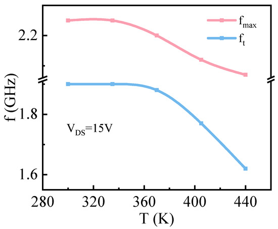
Figure 7 shows the simulation curve of the frequency characteristic of GaOPSiC devices considering SHE at = 15 V and temperatures ranging from 300 K to 440 K. As temperature increases, both the cut-off frequency (ft) and maximum operating frequency (fmax) exhibit decreasing trends. This phenomenon can be attributed to the direct proportionality between and , as derived from Equation (2) and the definition of [65,66].
As the temperature rises, the mobility of electrons decreases, which in turn leads to a reduction in , thereby causing the values of and to decrease as well.
By optimizing the thickness and doping concentration of the P-Ga2O3 buffer layer and the 4H-SiC substrate, two device structures were obtained: GaOPSiC1 and GaOPSiC2. Among these, GaOPSiC1 has = 4 × 1016 cm−3, and GaOPSiC1 has = 4 × 1016 cm−3, = 5.49 μm, and = 11 μm, exhibiting the lowest I and best thermal conductivity, while GaOPSiC2 has = 4 × 1016 cm−3, = 5.49 μm, and = 10 μm, with the highest breakdown voltage and PFOM. The performance parameters of the two devices are shown in Table 2.
Table 2.
Performance parameters of GaOPSiC1 and GaOPSiC2.
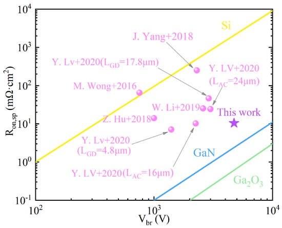
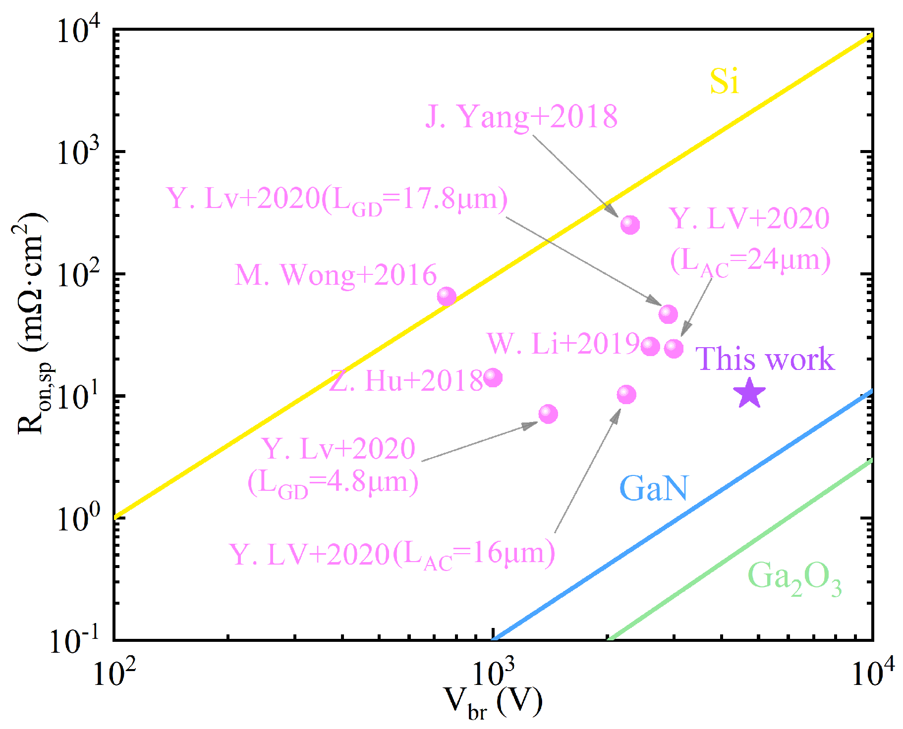
The breakdown voltage and the ratio of on-resistance are important parameters for evaluating the power quality factor of a device. To demonstrate the excellent performance of this structure, by referring to the literature, the experimental data of some published Ga2O3 MOSFET devices with Si or SiC heterojunction substrates were compared with the results of this structure. The results are shown in Figure 8. It can be seen that the breakdown voltage and the power quality factor of this structure are both relatively large, and it has broad application prospects in the high-voltage and high-power fields.
Figure 8.
Comparison of specific on-resistance () and breakdown voltage () between the device designed in this work (simulation results) and those of previously reported gallium oxide MOSFETs (experimental results) [11,18,20,67,68,69].
4. Conclusions
In this work, the hetero-integration of -Ga2O3 MOSFETs with a P-Ga2O3 buffer layer on AlN/SiC substrates is comprehensively investigated through TCAD simulations. By incorporating the p-type -Ga2O3 buffer layer, the device achieved of 4781 V, of 10.40 m·cm2, and PFOM of 2.20 GW/cm2. The utilization of AlN/SiC substrates significantly improved thermal management, reducing from 776.50 K to 570.90 K under ambient conditions of 300 K. Key performance metrics included of 1.52 V and an on/off ratio exceeding 9.20 × 10⁹. These advances enabled stable operation under high-voltage and high-temperature conditions, demonstrating substantial application potential in modern power electronic systems.
Author Contributions
W.L. and C.Z. contributed to the conceptualization and methodology of this study; D.W. developed the software and provided resources; W.L., C.Z. and Y.L. conducted the investigation and formal analysis; W.L., C.Z., Y.L., P.W. and G.W. were responsible for data curation; W.L. and P.W. performed validation; W.L. and Y.L. wrote the original draft; W.L. and C.Z. reviewed and edited the manuscript; D.W., C.Z., Y.L., P.W. and G.W., supervised the research; and C.Z. administered the project. All authors have read and agreed to the published version of the manuscript.
Funding
National Natural Science Foundation of China under Grants U21A20501, Innovation Capability Improvement Project of Hebei province China under Grants 22567605H, Supporting Programs for Special and Emerging Undergraduate Majors in General Colleges and Universities of Chongqing.
Institutional Review Board Statement
Not applicable.
Informed Consent Statement
Not applicable.
Data Availability Statement
All reasonable requests for materials should be directed to and will be fulfilled by the corresponding author.
Conflicts of Interest
The authors declare no conflicts of interest.
References
- Higashiwaki, M.; Sasaki, K.; Murakami, H.; Kumagai, Y.; Koukitu, A.; Kuramata, A.; Masui, T.; Yamakoshi, S. Recent progress in Ga2O3 power devices. Semicond. Sci. Technol. 2016, 31, 034001. [Google Scholar] [CrossRef] [Scilit]
- Dong, H.; Xue, H.W.; He, Q.M.; Qin, Y.; Jian, G.; Long, S.; Liu, M. Progress of power field effect transistor based on ultra-wide bandgap Ga2O3 semiconductor material. J. Semicond. 2019, 40, 011802. [Google Scholar] [CrossRef] [Scilit]
- Pearton, S.J.; Yang, J.; IV, P.H.C.; Ren, F.; Kim, J.; Tadjer, M.J.; Mastro, M.A. A review of Ga2O3 materials, processing, and devices. Appl. Phys. Rev. 2018, 5, 011301. [Google Scholar] [CrossRef] [Scilit]
- Lei, D.; Han, K.; Wu, Y.; Liu, Z.; Gong, X. High performance Ga2O3 metal-oxide-semiconductor field-effect transistors on an AlN/Si substrate. IEEE J. Electron Devices Soc. 2019, 7, 596–600. [Google Scholar] [CrossRef] [Scilit]
- Chen, W.; Chen, Z.; Li, Z.; Fei, Z.; Pei, Y.; Wang, G.; He, Z. Heteroepitaxy of ε-Ga2O3 thin films grown on AlN/Si(111) templates by metal-organic chemical vapor deposition. Appl. Surf. Sci. 2022, 581, 152335. [Google Scholar] [CrossRef] [Scilit]
- Li, Y.; Yang, C.; Wu, L.; Zhang, R. Electrical and optical properties of Si-doped Ga2O3. Mod. Phys. Lett. B 2017, 31, 1750172. [Google Scholar] [CrossRef] [Scilit]
- Higashiwaki, M.; Sasaki, K.; Kuramata, A.; Masui, T.; Yamakoshi, S. Gallium oxide (Ga2O3) metal-semiconductor field-effect transistors on single-crystal β-Ga2O3 (010) substrates. Appl. Phys. Lett. 2012, 100, 013504. [Google Scholar] [CrossRef] [Scilit]
- Qin, Y.; Dong, H.; Long, S.; He, Q.; Jian, G.; Zhang, Y.; Zhou, X.; Yu, Y.; Hou, X.; Tan, P.; et al. Enhancement-Mode β -Ga2O3 Metal-COxide-CSemiconductor Field-Effect Solar-Blind Phototransistor with Ultrahigh Detectivity and Photo-to-Dark Current Ratio. IEEE Electron Device Lett. 2019, 40, 742–745. [Google Scholar] [CrossRef] [Scilit]
- Higashiwaki, M.; Sasaki, K.; Kamimura, T.; Wong, M.H.; Krishnamurthy, D.; Kuramata, A.; Masui, T.; Yamakoshi, S. Depletion-mode Ga2O3 metal-oxide-semiconductor field-effect transistors on β-Ga2O3 (010) substrates and temperature dependence of their device characteristics. Appl. Phys. Lett. 2013, 103, 123511. [Google Scholar] [CrossRef] [Scilit]
- Green, A.J.; Chabak, K.D.; Heller, E.R.; Fitch, R.C.; Baldini, M.; Fiedler, A.; Irmscher, K.; Wagner, G.; Galazka, Z.; Tetlak, S.E.; et al. 3.8-MV/cm Breakdown Strength of MOVPE-Grown Sn-Doped β-Ga2O3 MOSFETs. IEEE Electron Device Lett. 2016, 37, 902–905. [Google Scholar] [CrossRef] [Scilit]
- Wong, M.H.; Sasaki, K.; Kuramata, A.; Yamakoshi, S.; Higashiwaki, M. Field-Plated Ga2O3 MOSFETs with a Breakdown Voltage of Over 750 V. IEEE Electron Device Lett. 2016, 37, 212–215. [Google Scholar] [CrossRef] [Scilit]
- Moser, N.; McCandless, J.; Crespo, A.; Leedy, K.; Green, A.; Neal, A.; Mou, S.; Ahmadi, E.; Speck, J.; Chabak, K.; et al. Ge-Doped β-Ga2O3 MOSFETs. IEEE Electron Device Lett. 2017, 38, 775–778. [Google Scholar] [CrossRef] [Scilit]
- Lv, Y.; Zhou, X.; Long, S.; Song, X.; Wang, Y.; Liang, S.; He, Z.; Han, T.; Tan, X.; Feng, Z.; et al. Source-Field-Plated β-Ga2O3 MOSFET with Record Power Figure of Merit of 50.4 MW/cm2. IEEE Electron Device Lett. 2018, 40, 83–86. [Google Scholar] [CrossRef] [Scilit]
- Chabak, K.D.; McCandless, J.P.; Moser, N.A.; Green, A.J.; Mahalingam, K.; Crespo, A.; Hendricks, N.; Howe, B.M.; Tetlak, S.E.; Leedy, K.; et al. Recessed-Gate Enhancement-Mode β-Ga2O3 MOSFETs. IEEE Electron Device Lett. 2018, 39, 67–70. [Google Scholar] [CrossRef] [Scilit]
- Zeng, K.; Wallace, J.S.; Heimburger, C.; Sasaki, K.; Kuramata, A.; Masui, T.; Gardella, J.A.; Singisetti, U. Ga2O3 MOSFETs Using Spin-On-Glass Source/Drain Doping Technology. IEEE Electron Device Lett. 2017, 38, 513–516. [Google Scholar] [CrossRef] [Scilit]
- Zeng, K.; Vaidya, A.; Singisetti, U. 1.85 kV Breakdown Voltage in Lateral Field-Plated Ga2O3 MOSFETs. IEEE Electron Device Lett. 2018, 39, 1385–1388. [Google Scholar] [CrossRef] [Scilit]
- Mun, J.K.; Cho, K.; Chang, W.; Jung, H.-W.; Do, J. 2.32 kV Breakdown Voltage Lateral β-Ga2O3 MOSFETs with Source-Connected Field Plate. ECS J. Solid State Sci. Technol. 2019, 8, Q3079. [Google Scholar] [CrossRef] [Scilit]
- Lv, Y.; Liu, H.; Zhou, X.; Wang, Y.; Song, X.; Cai, Y.; Yan, Q.; Wang, C.; Liang, S.; Zhang, J.; et al. Lateral β-Ga2O3 MOSFETs with High Power Figure of Merit of 277 MW/cm2. IEEE Electron Device Lett. 2020, 41, 537–540. [Google Scholar] [CrossRef] [Scilit]
- Sharma, S.; Zeng, K.; Saha, S.; Singisetti, U. Field-Plated Lateral Ga2O3 MOSFETs with Polymer Passivation and 8.03 kV Breakdown Voltage. IEEE Electron Device Lett. 2020, 41, 836–839. [Google Scholar] [CrossRef] [Scilit]
- Hu, Z.; Zhou, H.; Feng, Q.; Zhang, J.; Zhang, C.; Dang, K.; Cai, Y.; Feng, Z.; Gao, Y.; Kang, X.; et al. Field-Plated Lateral β-Ga2O3 Schottky Barrier Diode with High Reverse Blocking Voltage of More Than 3 kV and High DC Power Figure-of-Merit of 500 MW/cm2. IEEE Electron Device Lett. 2018, 39, 1564–1567. [Google Scholar] [CrossRef] [Scilit]
- Wang, X.; Faizan, M.; Na, G.; He, X.; Fu, Y.; Zhang, L. Discovery of New Polymorphs of Gallium Oxides with Particle Swarm Optimization-Based Structure Searches. Adv. Electron. Mater. 2020, 6, 2000119. [Google Scholar] [CrossRef] [Scilit]
- Lei, W.W.; Dang, K.; Zhou, H.; Zhang, J.; Wang, C.; Xin, Q.; Alghamdi, S.; Liu, Z.; Feng, Q.; Sun, R.; et al. Proposal and Simulation of Ga2O3 MOSFET with PN Heterojunction Structure for High-Performance E-Mode Operation. IEEE Trans. Electron Devices 2022, 69, 3617–3622. [Google Scholar] [CrossRef] [Scilit]
- Xu, W.; Hao, Y.; Wang, X.; Wang, Y.; You, T.; Ou, X.; Han, G.; Hu, H.; Shibin, Z.; Fengwen, M.; et al. First Demonstration of Waferscale Heterogeneous Integration of Ga2O3 MOSFETs on SiC and Si Substrates by Ion-Cutting Process. In Proceedings of the 2019 IEEE International Electron Devices Meeting (IEDM); IEEE: San Francisco, CA, USA, 2019; pp. 12.5.1–12.5.4. [Google Scholar] [CrossRef] [Scilit]
- Zhou, H.; Si, M.; Alghamdi, S.; Qiu, G.; Yang, L.; Ye, P.D. High-Performance Depletion/Enhancement-mode β-Ga2O3 on Insulator (GOOI) Field-Effect Transistors with Record Drain Currents of 600/450 mA/mm. IEEE Electron Device Lett. 2017, 38, 103–106. [Google Scholar] [CrossRef] [Scilit]
- Wang, Y.; Xu, W.; Han, G.; You, T.; Mu, F.; Hu, H.; Liu, Y.; Zhang, X.; Huang, H.; Suga, T.; et al. Channel Properties of Ga2O3-on-SiC MOSFETs. IEEE Trans. Electron Devices 2021, 68, 1185–1189. [Google Scholar] [CrossRef] [Scilit]
- Qu, Z.; Xie, Y.; Zhao, T.; Xu, W.; He, Y.; Xu, Y.; Sun, H.; You, T.; Han, G.; Hao, Y.; et al. Extremely Low Thermal Resistance of β-Ga2O3 MOSFETs by Co-integrated Design of Substrate Engineering and Device Packaging. ACS Appl. Mater. Interfaces 2024, 16, 57816–57823. [Google Scholar] [CrossRef] [Scilit]
- Wang, Y.; Xu, W.; You, T.; Mu, F.; Hu, H.; Liu, Y.; Huang, H.; Suga, T.; Han, G.; Ou, X.; et al. β-Ga2O3 MOSFETs on the Si substrate designed by the ion-cutting process. Sci. China Phys. Mech. Astron. 2020, 63, 277311. [Google Scholar] [CrossRef] [Scilit]
- Zeng, K.; Soman, R.; Bian, Z.; Jeong, S.; Chowdhury, S. Vertical Ga2O3 MOSFET with Magnesium Diffused Current Blocking Layer. IEEE Electron Device Lett. 2022, 43, 1527–1530. [Google Scholar] [CrossRef] [Scilit]
- Kim, I.K.; Cha, S.; Hong, S.-M. Optimization of Nitrogen Ion Implantation Condition for β-Ga2O3 Vertical MOSFETs via Process and Device Simulation. IEEE Trans. Electron Devices 2022, 69, 6948–6955. [Google Scholar] [CrossRef] [Scilit]
- Pearton, S.J.; Ren, F.; Tadjer, M.; Kim, J. Perspective: β-Ga2O3 for ultra-high power rectifiers and MOSFETs. J. Appl. Phys. 2018, 124, 220901. [Google Scholar] [CrossRef] [Scilit]
- Zhang, Y.; Alema, F.; Mauze, A.; Koksaldi, O.S.; Miller, R.; Osinsky, A.; Speck, J.S. MOCVD grown epitaxial β-Ga2O3 thin film with an electron mobility of 176 cm2/V s at room temperature. APL Mater. 2019, 7, 022506. [Google Scholar] [CrossRef] [Scilit]
- Jomaah, J.; Balestra, F.; Ghibaudo, G. Self-heating effects in SOI MOSFET’s operated at low temperature. In Proceedings of 1993 IEEE International SOI Conference; IEEE: New York, NY, USA, 1993; pp. 82–83. [Google Scholar] [CrossRef] [Scilit]
- Mani, P.; Pandey, M.K. Impact of Temperature on Threshold Voltage & Self Heating in Ultra Thin SOI MOSFET. In 2019 6th International Conference on Signal Processing and Integrated Networks (SPIN); IEEE: New York, NY, USA, 2019; pp. 796–798. [Google Scholar] [CrossRef] [Scilit]
- Kumar, A.; Srinivas, P.S.T.N.; Tiwari, P. An Insight into Self-heating Effects and its Implications on Hot Carrier Degradation for Silicon-Nanotube-Based Double Gate-All-Around (DGAA) MOSFETs. IEEE J. Electron Devices Soc. 2019, 7, 1. [Google Scholar] [CrossRef] [Scilit]
- Mahajan, B.K.; Chen, Y.-P.; Ahn, W.; Zagni, N.; Alam, M.A. Design and Optimization of β-Ga2O3 on (h-BN layered) Sapphire for High Efficiency Power Transistors: A Device-Circuit-Package Perspective. In Proceedings of the 2018 IEEE International Electron Devices Meeting (IEDM); IEEE: New York, NY, USA, 2018; pp. 24.6.1–24.6.4. [Google Scholar] [CrossRef] [Scilit]
- Wei, R.; Song, S.; Yang, K.; Cui, Y.; Peng, Y.; Chen, X.; Hu, X.; Xu, X. Thermal conductivity of 4H-SiC single crystals. J. Appl. Phys. 2013, 113, 053503. [Google Scholar] [CrossRef] [Scilit]
- Rafique, S.; Han, L.; Neal, A.T.; Mou, S.; Tadjer, M.J.; French, R.H.; Zhao, H. Heteroepitaxy of N-type β-Ga2O3 thin films on sapphire substrate by low pressure chemical vapor deposition. Appl. Phys. Lett. 2016, 109, 132103. [Google Scholar] [CrossRef] [Scilit]
- Zhao, Y.; Wu, Z.Y.; Liu, C.X.; Yue, X.F.; Chen, J.J.; Cong, C.X.; Wang, J.L.; Kang, J.Y.; Chu, J.H.; Fang, Z.L. β-Ga2O3 van der Waals p-n Homojunction. Mater. Today Phys. 2024, 44, 101447. [Google Scholar] [CrossRef] [Scilit]
- McGlone, J.F.; Xia, Z.B.; Joishi, C.; Lodha, S.; Rajan, S.; Ringel, S.; Arehart, A.R. Identification of critical buffer traps in Si δ-doped β-Ga2O3 mesfets. Appl. Phys. Lett. 2019, 115, 153501. [Google Scholar] [CrossRef] [Scilit]
- Kumar, A.; Berg, M.; Wang, Q.; Salter, M.; Ramvall, R. Growth of p-type GaN–The role of oxygen in activation of Mg-doping. Power Electron. Devices Compon. 2023, 5, 100036. [Google Scholar] [CrossRef] [Scilit]
- Ravariu, C.; Mihaiescu, D.E.; Morosan, A.; Istrati, D.; Purcareanu, B.; Cristescu, R.; Trusca, R.; Stefan Vasile, B. Solution for green organic thin film transistors: Fe3O4 nano-core with PABA external shell as p-type film. J. Mater. Sci. Mater. Electron. 2020, 31, 3063–3073. [Google Scholar] [CrossRef] [Scilit]
- Hoque, M.S.B.; Koh, Y.R.; Braun, J.L.; Mamun, A.; Liu, Z.; Huynh, K.; Liao, M.E.; Hussain, K.; Cheng, Z.; Hoglund, E.R.; et al. High In-Plane Thermal Conductivity of Aluminum Nitride Thin Films. ACS Nano 2021, 15, 9588–9599. [Google Scholar] [CrossRef] [Scilit]
- Disney, D.; Shen, Z.J. Review of Silicon Power Semiconductor Technologies for Power Supply on Chip and Power Supply in Package Applications. IEEE Trans. Power Electron. 2013, 28, 4168–4181. [Google Scholar] [CrossRef] [Scilit]
- Abouelatta-Ebrahim, M.; Shaker, A.; Sayah, G.T.; Gontrand, C.; Zekry, A. Design considerations of high voltage RESURF nLDMOS: An analytical and numerical study. Ain Shams Eng. J. 2015, 6, 501–509. [Google Scholar] [CrossRef] [Scilit]
- Ludikhuize, A.W. A review of RESURF technology. In Proceedings of the 12th International Symposium on Power Semiconductor Devices ICs. Proceedings (Cat. No.00CH37094); IEEE: New York, NY, USA, 2000; pp. 11–18. [Google Scholar] [CrossRef] [Scilit]
- Imam, M.L.; Quddus, M.; Adams, J.; Hossain, Z. Efficacy of charge sharing in reshaping the surface electric field in high-voltage lateral RESURF devices. IEEE Trans. Electron Devices 2004, 51, 141–148. [Google Scholar] [CrossRef]
- Abouelatta-Ebrahim, M.; Gontrand, C.; Zekry, A. Design of complementary LDMOS in 0.35 μm BiCMOS technology for smart integration. Eur. Phys. J. Appl. Phys. 2012, 57, 10103. [Google Scholar] [CrossRef] [Scilit]
- Xu, D.-Z.; Jin, P.; Xu, P.-F.; Feng, M.-Y.; Wu, J.; Wang, Z.G. Investigation of Ga2O3/diamond heterostructure solar-blind avalanche photodiode via TCAD simulation. Chin. Phys. B 2023, 32, 108504. [Google Scholar] [CrossRef] [Scilit]
- Nandi, A.; Rana, K.S.; Bag, A. Design and analysis of P-GaN/N-Ga2O3 based junction barrier schottky diodes. IEEE Trans. Electron Devices 2021, 68, 6052–6058. [Google Scholar] [CrossRef] [Scilit]
- Bennett, H.S.; Wilson, C.L. Statistical comparisons of data on bandgap narrowing in heavily doped silicon: Electrical and optical measurements. J. Appl. Phys. 1984, 55, 3582–3587. [Google Scholar] [CrossRef] [Scilit]
- Klaassen, D.B.M. A unified mobility model for device simulation—I. Model equations and concentration dependence. Solid-State Electron. 1992, 35, 953–959. [Google Scholar] [CrossRef] [Scilit]
- Arora, N.D.; Hauser, J.R.; Roulston, D.J. Electron and hole mobilities in silicon as a function of concentration and temperature. IEEE Trans. Electron Devices 1982, 29, 292–295. [Google Scholar] [CrossRef] [Scilit]
- Roulston, D.J.; Arora, N.D.; Chamberlain, S.G. Modeling and measurement of minority-carrier lifetime versus doping in diffused layers of n+-p silicon diodes. IEEE Trans. Electron Devices 1982, 29, 284–291. [Google Scholar] [CrossRef]
- McIntyre, R.J. On the avalanche initiation probability of avalanche diodes above the breakdown voltage. IEEE Trans. Electron Devices 1973, 20, 637–641. [Google Scholar] [CrossRef] [Scilit]
- Wachutka, G.K. Rigorous thermodynamic treatment of heat generation and conduction in semiconductor device modeling. IEEE Trans.-Comput.-Aided Des. Integr. Circuits Syst. 1990, 9, 1141–1149. [Google Scholar] [CrossRef] [Scilit]
- Ma, N.; Tanen, N.; Verma, A.; Guo, Z.; Luo, T.; Xing, H.G.; Jena, D. Intrinsic electron mobility limits in β-Ga2O3. Appl. Phys. Lett. 2016, 109, 212101. [Google Scholar] [CrossRef] [Scilit]
- Xiao, M.; Palacios, T.; Zhang, Y. ON-resistance in vertical power FinFETs. IEEE Trans. Electron Devices 2019, 66, 3903–3909. [Google Scholar] [CrossRef] [Scilit]
- García, G.I.M.; Khandelwal, V.; Mainali, G.; Paulín, V.D.; Sarkar, B.; Li, X. Lateral semiconductor–free-space gate transistors. Nano Lett. 2025, 25, 15579–15584. [Google Scholar] [CrossRef] [Scilit]
- Taur, Y. An analytical solution to a double-gate MOSFET with undoped body. IEEE Electron Device Lett. 2000, 21, 245–247. [Google Scholar] [CrossRef] [Scilit]
- Rahman, T.; Hossain, M.M.; Rasheduzzaman, M. Effects of channel length and oxide layer modulation on the performance of β-Ga2O3 MOSFET. In Proceedings of the 2021 IEEE International Conference on Power, Electrical, Electronic and Industrial Applications (PEEIACON); IEEE: New York, NY, USA, 2021; pp. 25–28. [Google Scholar] [CrossRef] [Scilit]
- Narasimhan, T.N. Fourier’s heat conduction equation: History, influence, and connections. Proc. Indian Acad. Sci. Earth Planet. Sci. 1999, 108, 117–148. [Google Scholar] [CrossRef] [Scilit]
- Al-Saman, A.A.; Pei, Y.; Ryndin, E.A.; Lin, F. Accurate Temperature Estimation for Each Gate of GaN HEMT with n-Gate Fingers. IEEE Trans. Electron Devices 2020, 67, 3577–3584. [Google Scholar] [CrossRef] [Scilit]
- Li, Y.; Fang, Y.; Cai, Z.; Luan, T.; Sang, L. Polycrystalline diamond heteroepitaxy on the third-generation semiconductors for thermal dissipation. Mater. Today Electron. 2026, 16, 100207. [Google Scholar] [CrossRef] [Scilit]
- Han, Y.; Jiao, T.; Yu, H.; Sai, Q.; Chen, D.; Li, Z.; Li, Y.; Zhang, Z.; Dong, X. Effect of Substrate Crystal Planes on the Properties of Homoepitaxial n-Ga2O3 Thin Films Grown by MOCVD. J. Synth. Cryst. 2025, 54, 438–444. [Google Scholar]
- Flandre, D.; Raskin, J.-P.; Vanhoenacker-Janvier, D. SOI CMOS Transistors for RF and Microwave Applications. In CMOS RF Modeling, Characterization and Applications; World Scientific Publishing Company: Singapore, 2002; pp. 273–362. [Google Scholar] [CrossRef] [Scilit]
- Lu, K.; Chen, J.; Luo, J.; Liu, J.; Wu, Q.; Chai, Z.; Wang, X. Improvement of RF Performance by Using Tunnel Diode Body Contact Structure in PD SOI nMOSFETs. IEEE Electron Device Lett. 2014, 35, 15–17. [Google Scholar] [CrossRef] [Scilit]
- Li, W.; Nomoto, K.; Hu, Z.; Nakamura, T.; Jena, D.; Xing, H.G. Single and multi-fin normally-off β-Ga2O3 vertical transistors with a breakdown voltage over 2.6 kV. In Proceedings of the 2019 IEEE International Electron Devices Meeting (IEDM); IEEE: New York, NY, USA, 2019; pp. 12.4.1–12.4.4. [Google Scholar] [CrossRef] [Scilit]
- Yang, J.; Ren, F.; Tadjer, M.; Pearton, S.J.; Kuramata, A. 2300 V reverse breakdown voltage β-Ga2O3 Schottky rectifiers. ECS J. Solid State Sci. Technol. 2018, 7, Q92. [Google Scholar] [CrossRef] [Scilit]
- Hu, Z.; Nomoto, K.; Li, W.; Tanen, N.; Sasaki, K.; Kuramata, A.; Nakamura, T.; Jena, D.; Xing, H.G. Enhancement-Mode β-Ga2O3 Vertical Transistors with Breakdown Voltage >1 kV. IEEE Electron Device Lett. 2018, 39, 869–872. [Google Scholar] [CrossRef] [Scilit]

Disclaimer/Publisher’s Note: The statements, opinions and data contained in all publications are solely those of the individual author(s) and contributor(s) and not of MDPI and/or the editor(s). MDPI and/or the editor(s) disclaim responsibility for any injury to people or property resulting from any ideas, methods, instructions or products referred to in the content. |
© 2026 by the authors. Licensee MDPI, Basel, Switzerland. This article is an open access article distributed under the terms and conditions of the Creative Commons Attribution (CC BY) license.