


Abstract
Through-glass vias (TGVs), as key vertical interconnect structures in 2.5-D/3-D advanced packaging, offer low dielectric loss, low parasitic capacitance, and excellent high-frequency transmission performance. However, several challenges remain in TGV metallization, including (1) incontinuity of seed layers in high aspect ratio TGVs; (2) non-uniform distributions of copper-ion concentration and current density, leading to significant differences in copper deposition rates between the via interior and the via opening; (3) voids, seams, and double bridging caused by excessively rapid deposition at the via opening or poor control of the central bridging position; and (4) low filling rate and resulting high cost. This article reviews the research progress in TGV metallization to address the above issues. Several electroless plating studies were reported to improve the seed layer continuity and uniformity. Adjusting the concentrations of copper ions, chloride ions, accelerators, suppressors, and levelers in the plating bath are the keys to regulating the deposition rates at the via opening, via walls, and via center. Electroplating strategies, including pulsed electroplating and multistage electroplating, can optimize the electric-field distribution inside the vias. Ultrasonic agitation enhances forced convection within the vias and thereby improves mass-transport conditions. In summary, this paper reviews the research progress in TGV metallization, with emphasis on these key challenges and corresponding solutions, and discusses their prospects for high-density interconnects in advanced packaging.
1. Introduction
With the continued development of 5G communications, the Internet of Things, and artificial intelligence, advanced packaging has become an important means of extending integration beyond conventional transistor scaling. Through-glass vias (TGVs) are promising vertical interconnects for 2.5-D and 3-D packaging because glass offers high electrical resistivity, low parasitic capacitance, favorable high-frequency performance, and a tunable coefficient of thermal expansion [1,2,3]. The increasing demand for compact, high-density interconnects has driven reductions in via diameter; when substrate thickness remains largely unchanged, this correspondingly increases the via aspect ratio [4]. However, reliable metallization of high-aspect-ratio TGVs remains challenging. The electrically insulating glass requires continuous barrier and seed layers, while restricted mass transport, nonuniform current distribution, and additive interactions can cause nonuniform Cu deposition, premature closure, voids, seams, and double bridging. Although complete filling is preferred when low electrical resistance and efficient heat conduction are required, conformal, partial, and bridge-assisted filling may be more suitable for applications prioritizing reduced Cu consumption, shorter processing time, or thermomechanical reliability [3,5].
This review summarizes recent advances in high-aspect-ratio TGV metallization. Section 2 discusses barrier- and seed-layer preparation. Section 3 reviews butterfly filling and the effects of bath composition, additives, current waveforms, and mass transport, as well as methods for screening and optimizing process parameters. Section 4 examines via geometry and alternative filling strategies in relation to filling behavior and interconnect performance. Through this framework, the review clarifies the coupled roles of seed-layer quality, plating chemistry, additive formulation, current waveform, mass transport, via geometry, and filling mode in determining TGV filling quality, process efficiency, electrical performance, and thermomechanical reliability.
2. Seed-Layer Enhancement for High-Aspect-Ratio TGVs
Because glass is intrinsically electrically insulating, metal ions cannot be directly reduced and deposited onto the highly resistive glass substrate. Therefore, a barrier layer and a seed layer must be prepared on the glass surface and the via sidewalls before Cu filling of the TGVs. The barrier layer is used to suppress Cu diffusion into the glass substrate and improve the interfacial adhesion between the metal layer and the glass substrate. Common barrier materials include Ta, Ti, and their nitrides. The seed layer provides a continuous conductive interface for subsequent Cu electroplating.
The existing processes for preparing barrier and seed layers mainly include sputtering, physical vapor deposition (PVD), chemical vapor deposition (CVD), atomic layer deposition (ALD), and electroless plating. PVD is widely used because it produces high-purity films with controllable composition and thickness. Sputtering, a common PVD technique, ejects target atoms through bombardment by plasma ions, which subsequently deposit on the substrate; magnetron sputtering increases the deposition rate by enhancing plasma density near the target [6,7,8]. The mature equipment, relatively high deposition rate, and scalability of sputtering make it suitable for barrier- and seed-layer deposition [7,8,9,10]. However, its line-of-sight deposition can cause shadowing by the via opening and upper sidewalls, resulting in thin or discontinuous coverage near the bottom of high-aspect-ratio vias [11,12,13]. Substrate rotation or tilting, collimation, ionized PVD, or electroless post-deposition can improve coverage [12,13].
In contrast, CVD forms films through reactions between gaseous precursors and the substrate surface. Because the precursors can reach recessed regions from multiple directions, CVD generally provides better conformality than conventional sputtering and is suitable for three-dimensional, high-aspect-ratio structures [14,15,16]. Its application may nevertheless be constrained by substrate-temperature requirements, precursor chemistry, and the management of hazardous by-products [15,16].
ALD is a cyclic vapor-phase deposition process based on sequential, self-limiting surface reactions. In a typical cycle, a first precursor is introduced and adsorbs onto available surface sites. After excess precursor and gaseous by-products are purged, a second reactant is introduced to react with the adsorbed species and form the desired solid compound; a subsequent purge removes residual reactants and products. Because each half-reaction terminates when the available reactive sites are saturated, repeated cycles deposit the film in a controlled, layer-by-layer manner [17,18]. Film thickness can therefore be controlled by adjusting the number of cycles. Moreover, precursor diffusion into narrow features, combined with the self-limiting nature of the surface reactions, enables highly conformal coatings with nearly uniform thickness along the via opening, sidewalls, and bottom, including in high-aspect-ratio structures [19,20]. The advantages and limitations of these deposition methods are summarized in Table 1.
Table 1.
Comparison of common thin-film preparation processes.
Because of the limited step coverage of sputtering equipment, some high-aspect-ratio through-vias are difficult to coat with continuous and uniform metal films [21,22]. In recent years, electroless plating has been regarded as a potential alternative for preparing metal seed layers in TGV metallization [5,23,24]. This method enables the deposition of dense metal films with low porosity at room temperature and under nonvacuum conditions. Chen et al. proposed a palladium-free, low-cost, and environmentally friendly electroless Ni–P process for high-aspect-ratio TGVs and obtained a complete and continuous seed layer in TGVs with an aspect ratio of 10:1 [23]. However, because the redox reactions involved in electroless plating are accompanied by hydrogen evolution, gas bubbles can form during the process. These bubbles readily adhere to the cathodic surface and hinder the deposition of metal ions, resulting in defects such as voids and gaps in the deposited film and consequently affecting its integrity and uniformity. To address this issue, Huang et al. proposed a palladium-free activation and electroless silver-plating process based on the silver-mirror reaction, with glucose used as the reducing agent. Because the solubility of NH3 generated during the silver-mirror reaction in water is significantly higher than that of H2, this method can reduce gas-bubble-induced skip-plating defects [24]. Overall, electroless plating can improve the coverage continuity and uniformity of seed layers in high-aspect-ratio TGVs. However, hydrogen evolution, bubble-induced local skip-plating, and limited bath stability may still affect seed-layer quality. Therefore, after seed-layer preparation, the subsequent Cu-filling process requires the coordinated optimization of plating-bath composition, electroplating waveform, and intravia mass-transport conditions to achieve uniform and void-free Cu deposition.
3. Butterfly Filling of High-Aspect-Ratio TGVs
The primary Cu-filling mechanisms for glass microvias include bottom-up filling, conformal filling, and butterfly filling, each of which is applicable to different via geometries. Butterfly filling is currently the predominant strategy for filling high-aspect-ratio through-vias. Because TGVs are double-sided open through-vias without a blind-via bottom, the conventional bottom-up filling mechanism cannot be directly applied. Conformal filling, which requires comparable Cu deposition rates at the via opening, sidewalls, and interior, is prone to overgrowth at the opening, premature closure, and internal voids or seams under high-aspect-ratio conditions because of electric-field concentration and restricted intravia mass transport [25,26]. By contrast, butterfly filling uses additives and electroplating waveforms to establish a deposition-rate gradient in which Cu deposits preferentially at the via center, forming a bridge that converts the TGV into two blind vias; subsequent bottom-up filling then completes the metallization [25,26,27]. This combination of structural compatibility, defect suppression, and high-aspect-ratio filling capability has made butterfly filling a widely adopted strategy for vertical high-aspect-ratio TGVs [26,27].
The butterfly-filling process can be divided into two stages: bridge formation and bottom-up filling. As described above, TGVs are through-vias open on both sides, whereas bottom-up filling is commonly used for blind vias. Therefore, during the bridge-formation stage of butterfly filling, additives and electroplating waveforms are used to regulate the Cu deposition rates at the middle of the TGV sidewalls and at the via opening. The deposition rate at the via center is thereby made higher than that at the via opening, resulting in preferential deposition at the middle of the via. This process continues until the Cu layers growing from the two sidewalls meet and form a bridge, thereby dividing the TGV into two blind vias, as shown in Figure 1a,b. The subsequent bottom-up filling stage is similar to the bottom-up filling mechanism described above. In this stage, additives are used to control the upward Cu deposition inside the two blind vias. The process is illustrated in Figure 1c,d.
Figure 1.
Schematic illustration of butterfly filling: (a) straight through-via; (b) bridge formation stage, in which Cu deposits grow inward from the opposing sidewalls toward the via center (arrows); (c) bridge reinforcement stage, in which Cu deposition proceeds upward and downward from the bridge into the two blind vias (arrows); (d) filling stage for complete filling.
The key to butterfly filling is preferential deposition at the middle of the through-via, whereas conformal filling requires the deposition rates inside the via and at the via opening to remain comparable. The conformal filling capability is evaluated by the throwing power, which is defined in Equation (4). The control strategies for butterfly and conformal filling can be classified into several categories, including optimization of additives and their concentration ratios, adjustment of the current and potential parameters during electroplating, application of pulsed electroplating, enhancement of mass transport inside the TGVs, and optimization of via geometry. The primary difference lies in the direction of process regulation. In addition, to balance the filling time and filling quality required for complete filling of high-aspect-ratio TGVs, Fey et al. proposed a multistep electroplating strategy in which a low current is used for bridge formation and a high current is applied to accelerate sidewall filling [28]. The research status of these process technologies is discussed in detail in the following sections.
3.1. Optimization of Base Plating-Bath Composition and Parameters
Copper electroplating baths mainly include cyanide, pyrophosphate, and acidic systems. Because cyanide systems are highly toxic and generate difficult-to-treat wastewater, while pyrophosphate systems suffer from poor coating adhesion and limited bath stability, acidic copper plating has become dominant owing to its low cost, high current efficiency, and rapid deposition rate. Acidic baths generally contain a base electrolyte and additives [27]. The base electrolyte consists mainly of a copper salt and an acid. The copper salt supplies Cu ions, and its concentration directly affects the cathodic reduction and Cu deposition rates. The acid increases solution conductivity, lowers the cell voltage, suppresses Cu-ion hydrolysis, and improves bath stability [29,30]. These effects are important for regulating Cu-ion availability and local deposition kinetics during TGV filling.
Copper sulfate is the most widely used acidic plating system, whereas copper methanesulfonate (CuMSA) is mainly used for TSV and damascene filling. Using a CuMSA bath with MTT as the sole organic additive, Fey et al. achieved void-free filling of TGVs with an aspect ratio of 10:1. Compared with the copper sulfate system, CuMSA provided higher Cu-ion solubility, faster filling, and fewer additive-derived organic impurities in the deposit. This behavior was attributed to the weakly acidic MSA environment, which reduced formazan formation from MTT reduction and increased its solubility at low pH [28]. Thus, CuMSA is advantageous for rapid TGV filling, whereas copper sulfate offers more mature processing technology and greater industrial experience.
Sulfuric acid is the most common acid in copper sulfate baths, although formic, acetic, and propionic acids have also been investigated. Wang et al. compared these acid systems under matched hydrogen-ion concentrations and found that only the sulfuric acid bath achieved void-free TSV filling at a low current density of 0.5 A/dm2. The sulfuric acid system therefore provided the best filling performance and was particularly suitable for low-current-density operation [31].
Acid concentration can also interact strongly with the additives. Liang et al. investigated sulfuric acid concentration in a copper sulfate bath containing NTBC using a butterfly-filling strategy, in which a bridge formed at the via center before filling proceeded from both sides. Increasing the sulfuric acid concentration initially increased the filling rate, reduced defects, and enhanced NTBC suppression. These effects were optimized at 0.36 mol/L. Further increases caused excessive inhibition of the via wall and reduced the filling rate [32]. These results show that optimizing the base salt, acid type, and acid concentration can regulate Cu-ion availability and additive activity, thereby improving bridge formation and subsequent filling in high-aspect-ratio TGVs.
3.2. State of Research on Additives
As the aspect ratio of TGVs increases and their diameter decreases, mass transfer inside the vias becomes increasingly restricted. Cu-ion depletion and concentration gradients then develop, while the current density and deposition rate remain higher near the via opening than inside the via. Excessive deposition at the opening can cause premature closure and internal voids, compromising interconnect reliability. Additives are therefore used to regulate Cu-ion transport and interfacial deposition kinetics, thereby enabling butterfly or conformal filling. The main additives include chloride ions, accelerators, suppressors, and levelers.
3.2.1. Chloride Ions
Chloride ions can enhance anode activity, prevent anodic passivation, and serve as ionic bridges during the Cu2+/Cu+ reaction [33,34]. At an appropriate concentration, chloride ions can accelerate the Cu-reduction reaction [35,36]. They can also form complexes with accelerators and suppressors, thereby providing active sites for additive adsorption [37]. Through synergistic interactions, chloride ions further regulate the adsorption and desorption behavior of additives [38,39], thereby improving the quality of through-via filling.
Chloride ions activate the anode, prevent passivation, and regulate Cu electrodeposition by participating in the Cu2+/Cu+ reaction and promoting additive adsorption [33,34,35,36,37,38,39]. Their effect is concentration-dependent. At low concentrations (≤10 mM), adsorbed CuCl intermediates facilitate electron transfer and accelerate deposition. At high concentrations (≥100 mM), soluble copper–chloride complexes and a CuCl precipitate layer hinder Cu2+ reduction and produce an inhibiting effect [35]. Thus, chloride ions have a narrow process window and limited direct influence on the plating current. Their primary function is to provide adsorption sites and regulate the synergistic behavior of accelerators and suppressors, thereby controlling the deposition-rate distribution required for butterfly and bottom-up filling.
3.2.2. Accelerators
Accelerators increase the local Cu deposition rate by adsorbing onto the Cu surface, facilitating interfacial charge transfer, and/or stabilizing reactive Cu(I) intermediates. In high-aspect-ratio TGV filling, under ideal conditions, the accelerator is preferentially distributed in the central region of the via, thereby promoting bridge formation at the via center and subsequent Cu deposition at the via bottom after bridge formation. This preferential distribution helps compensate for the slower interfacial reaction kinetics in these regions, establishes a deposition-rate difference between the via opening and the via interior, and enables butterfly or superconformal filling. Common accelerators include bis(3-sulfopropyl) disulfide (SPS) and sodium 3-mercapto-1-propanesulfonate (MPS), although their action mechanisms remain under debate. Stoychev et al. attributed SPS acceleration to sulfur adsorption and enhanced electron transfer through the electrical double layer [40]. Kim et al. proposed that SPS first diffuses into the via and is subsequently converted to MPS through cathodically induced S–S bond cleavage; the generated MPS then catalyzes Cu reduction [41]. These two mechanisms emphasize either direct interfacial electron transfer or in situ conversion of SPS to MPS.
As noted above, chloride ions can act synergistically with other additives to enable butterfly and bottom-up filling. Tan et al. demonstrated that Cl− is essential for SPS and MPS to function as accelerators [42]. Without Cl−, these molecules form a blocking organic film on the Cu surface and suppress Cu2+ reduction. Cl− disrupts this film, while the displaced sulfonate groups coordinate with Cu2+/Cu+ and promote electron transfer. SPS and MPS therefore change from suppressors to accelerators, with the acceleration increasing as their concentration rises. This Cl−–accelerator synergy is essential for establishing the deposition-rate gradient required for butterfly and bottom-up filling.
The synergistic effect of Cl− on SPS and MPS is closely related to the molecular structure of the accelerator. In particular, the alkyl-chain length may affect adsorption and competition with PEG. To clarify this structure–property relationship, Li et al. compared SPS, bis(2-sulfoethyl) disulfide (SES), and bis(6-sulfohexyl) disulfide (SHS), whose alkyl chains contain three, two, and six carbon atoms, respectively [43]. In the absence of Cl−, all three accelerators formed blocking films on the Cu surface, and the suppressing effect increased with chain length. After Cl− was introduced, all three exhibited depolarizing behavior, with SHS showing the strongest Cl−-dependent acceleration. However, in the presence of PEG, SPS most effectively competed with and disrupted the PEG–Cl− blocking film. These results demonstrate that alkyl-chain length is an important parameter in accelerator design and help explain why SPS is widely used, particularly in PEG-containing plating systems.
Conventional accelerators such as MPS and SPS have narrow process windows and strong dependence on convective mass transport. Novel alternatives include DPS, TBPS, and the mercaptopropane dicopper complex MA [44,45,46]. Lan et al. reported a throwing power of 72% for through-holes with an aspect ratio of 10:1 in PCB test coupons using MA. Compared with SPS, MA reached adsorption equilibrium and a stable deposition potential more rapidly, required no intermediate activation reaction, and achieved a comparable depolarization effect at a lower concentration. MA therefore improves bath efficiency and reduces the need for frequent replenishment [47].
Restricted mass transport in deep, narrow TGVs can hinder accelerator transport to the via center, where preferential deposition is required for butterfly filling. To address this limitation, Chan et al. and Liu et al. reported TBPS, which has a lower dependence on mass transport than the conventional accelerator SPS, and further investigated the effects of Cl−, sulfuric acid concentration, and PEG on its electrochemical behavior and filling performance [44,48]. The disulfide bond in SPS can generate MPS and other sulfur-containing byproducts during bath cycling, whereas TBPS contains a more stable thioether linkage and exhibits higher resistance to anodic oxidation. TBPS therefore provides better bath stability and a longer service life. In addition, SPS and MPS may become suppressive at low concentrations, whereas TBPS retains strong accelerating activity under the low-concentration conditions inside high-aspect-ratio TGVs. TBPS is therefore more suitable for promoting preferential deposition at the via center and improving butterfly filling.
Cho et al. showed that DPS, which contains a dithiocarbamate structure, adsorbs strongly on the Cu surface through the lone-pair electrons of its nitrogen atoms. This adsorption suppresses Cu-adatom surface diffusion, allowing DPS to function as both an accelerator and a leveler. Compared with SPS, DPS produces smoother Cu deposits with lower surface roughness and resistivity while eliminating the need for an additional leveler and reducing organic contamination [46,49]. Lee et al. attributed the accelerating effect of DPS to the formation of a stable Cu(I)(DPS)2 complex, which stabilizes the Cu+ intermediate and facilitates the conversion of Cu2+ to Cu+, thereby accelerating Cu electrodeposition [50].
Building on the structure–property relationship of DPS, Wang et al. developed ETPS, an accelerator containing a dithioester group (–C(=S)–S–). At the same concentration, ETPS provided stronger acceleration than MPS, promoted the low-energy Cu(111) orientation more effectively than SPS, and produced a smoother deposit [51]. The Cu(111)-dominated and smoother Cu layer is more uniform and stable, which is beneficial for high-frequency signal transmission and lower resistivity [52,53,54].
3.2.3. Suppressors
Suppressors are generally species capable of adsorbing onto the Cu surface. Polyethylene glycol (PEG), the most widely used long-chain polyether suppressor, is a representative example. In PEG-containing baths, interactions between PEG, chloride ions, and interfacial Cu(I) species promote the formation and stabilization of a PEG–Cu–Cl passivating film, thereby reducing the local Cu deposition rate and regulating the deposition-rate difference between the via opening and the via interior. Suppressors are typically long-chain polymers, with polyethylene glycol (PEG) being widely used. PEG suppression depends on Cl−. PEG adsorption and suppression are potential-dependent both with and without Cl−. The presence of Cl− strengthens PEG adsorption and broadens the potential range over which suppression is maintained. Adsorbed Cl− interacts electrostatically with PEG–Cu+ species and stabilizes Cu+ against reduction, enabling the PEG film to remain stable at high cathodic overpotentials and form a strongly adherent, well-covered suppressing layer. Feng et al. confirmed using in situ surface-enhanced Raman spectroscopy that PEG suppression involves a ternary PEG–Cu–Cl complex and requires the simultaneous presence of Cl− and Cu+ [55]. Hebert further reported that a Cl− concentration above 1 mM is sufficient to stabilize the PEG suppressing layer [56].
Although the formation of the PEG suppressing film depends on the synergistic interaction of Cl− and Cu+, the effectiveness of PEG in deep vias is also governed by its molecular transport and adsorption behavior. PEG molecular weight is therefore an important parameter because it affects both diffusion into the vias and the resulting suppression strength. Dow et al. investigated the effect of PEG molecular weight on bottom-up filling in microblind vias. At a fixed PEG concentration of 200 ppm, the molecular weight was varied from 200 to 20,000 g/mol. PEG molecular weight strongly affected both suppression strength and filling performance, with an optimum range of 6000–8000 g/mol. Below 600 g/mol, PEG could not establish effective synergy with the accelerator, preventing bottom-up filling. Above 8000 g/mol, filling performance deteriorated because the strong convection dependence of high-molecular-weight PEG caused suppression at the via bottom and weakened the deposition-rate gradient required for bottom-up filling [57]. Because bridge formation converts a TGV into two blind vias, these results provide guidance for the subsequent filling stage of butterfly deposition.
In addition to molecular weight, the filling behavior of PEG is strongly influenced by its competitive interaction with accelerator molecules, particularly SPS. In PEG–Cl–SPS baths, PEG and SPS compete for adsorption sites. PEG first forms a passivating film through its synergistic interaction with Cl− and interfacial Cu+, whereas SPS can displace this film and accelerate Cu deposition [43,58].
Because the balance between PEG suppression and SPS acceleration depends on via geometry, the optimum additive ratio is not universal. Shin et al. identified an optimum PEG/SPS ratio of 500/5 ppm for TSVs with an aspect ratio of 3:1, whereas Dow et al. achieved defect-free superfilling of microblind vias using 200 ppm PEG and 1 ppm SPS, together with Cl− and DB [59,60]. These results show that PEG/SPS formulations must be tailored to the via geometry, although their competitive and synergistic interaction remains the basis for process optimization.
To quantitatively describe how PEG–SPS competitive adsorption promotes bottom-up filling, Moffat et al. described bottom-up superfilling using the curvature-enhanced adsorbate coverage (CEAC) model [61]. The model combines competitive adsorption with the change in interfacial area during nonplanar growth and assumes that the local deposition rate is proportional to the surface coverage of the accelerator. With conservation of adsorption sites, the coverage parameters of SPS and PEG can be obtained from planar-electrode data, and the evolution equation for SPS coverage can be derived as Equation (1).
Equation (1) is the core equation of the CEAC model, where θSPS denotes the SPS surface coverage 0 ≤ θSPS ≤ 1, t is time, kads and kinc are the rate constants for SPS adsorption and incorporation/deactivation, respectively, CSPS is the SPS concentration at the electrode interface, q is the reaction order of SPS consumption, v is the normal interfacial growth rate, and κ is the local interfacial curvature. The three terms on the right-hand side represent SPS adsorption, incorporation/deactivation, and curvature-induced geometric modulation associated with changes in interfacial area, respectively. The model assumes that interfacial curvature redistributes SPS, causing it to accumulate preferentially in concave regions and become relatively diluted in convex regions. During blind-via filling, the increasing SPS coverage at the via bottom enhances the local copper deposition rate, thereby establishing a positive feedback that drives bottom-up filling. The model is primarily used to explain blind-via filling and may also provide a theoretical basis for the second stage of butterfly filling in TGVs.
In the PEG–Cl–SPS system, Cl− provides the adsorption sites required for PEG and SPS. However, Cl− transport is limited inside high-aspect-ratio TGVs. Under low-Cl− conditions, the system may exhibit multiple steady states and hysteresis; once activated, it is difficult to recover its suppressing behavior, leading to uncontrolled wall deposition, premature closure at the via opening, and internal voids [56].
The CDA model explains this behavior through the convection-dependent adsorption of additives. Strong convection near the via opening promotes Cl− and PEG adsorption and strengthens suppression, whereas weak convection inside the via reduces suppression. Additive depletion therefore creates a deposition-rate difference between the via interior and the opening. Because SPS and PEG cannot be replenished rapidly in deep, narrow vias, the PEG–Cl–SPS system becomes increasingly difficult to control as the aspect ratio increases.
Two strategies have therefore been proposed: enhancing intravia mass transport through forced convection and pulse-reverse electroplating and developing suppressors with stronger inhibition and lower dependence on additive concentration and convection.
To overcome the strong convection dependence and narrow process window of conventional PEG suppressors, EO–PO-based polyethers have been explored as alternatives. Xiao et al. evaluated EPE2900, an EO–PO–EO triblock copolymer, and found that the filling defects decreased with increasing concentration and reached a minimum at 100 ppm but increased again at 200 ppm because the suppression difference between the panel surface and the via interior became insufficient. Compared with PEG, EPE2900 showed weaker convection-dependent adsorption and a wider process window [62]. Zhang et al. compared EO–PO random copolymers with different molecular weights under DC and PPR electroplating conditions. Like PEG, EO–PO requires Cl− and interfacial Cu(I) for adsorption and exhibits negligible suppression in chloride-free baths. Under DC conditions, lower-molecular-weight EO–PO produced stronger suppression because its faster diffusion and lower steric hindrance enabled greater surface coverage [63]. These studies indicate that both the concentration and molecular weight of EO–PO-based suppressors must be optimized to balance suppression strength, intravia diffusion, and deposition-rate control.
To improve the adsorption and transport behavior of polyether suppressors, Han et al. developed alkyl-terminated methoxy polyethylene glycol (MPEG-AC), including butyl-terminated MPEG-Bu, by replacing the terminal hydroxyl groups of MPEG with alkyl groups. Compared with conventional MPEG, MPEG-Bu exhibited stronger adsorption on the Cu surface because its hydrophobic butyl groups interacted favorably with the hydrophobic interface formed by adsorbed Cl−. Both adsorption and suppression increased with alkyl-chain length [64]. Han et al. subsequently compared MPEG and MPEG-Bu with molecular weights of 1000, 2000, and 5000 Da. Among the tested MPEG-Bu suppressors, the 1000 Da variant provided the highest throwing power in PCB through-holes with aspect ratios of 6:1 and 10:1, exceeding 80% in both cases. These results from PCB through-hole electroplating suggest that low-molecular-weight MPEG-Bu may also be a promising suppressor for high-aspect-ratio TGV electroplating, although its applicability to TGVs requires direct experimental validation.
Tetrazole-based levelers are widely used to induce butterfly filling and are discussed in the following section. Polyether suppressors provide an alternative approach. Jin et al. achieved void-free butterfly filling of TGVs with an aspect ratio of 5:1 using a PEG–SPS–PVP bath [65]. The S-NDR model employed by Braun et al. explains how polyether suppressors establish the deposition-rate gradient required for butterfly filling. At sufficiently negative potentials, the Cl−–polyether-suppressing film breaks down. Because convection is weak at the via center, Cl− and suppressor molecules cannot be replenished effectively, preventing film re-formation and leaving the center in an activated state. Near the via opening, stronger convection enables rapid replenishment and re-formation of the suppressing film, keeping this region passivated. Consequently, Cu deposits preferentially at the via center while deposition near the opening is suppressed, leading to butterfly filling. The different potentials for film breakdown and re-formation produce a hysteresis loop during reverse potential scanning, providing evidence for the S-NDR mechanism [66].
3.2.4. Levelers
Levelers are organic additives that preferentially adsorb at protrusions and via openings, where the local current density or cathodic overpotential is typically high. By blocking active Cu-reduction sites and/or restricting surface diffusion, levelers selectively suppress localized overgrowth, improve deposit uniformity, and help establish a deposition-rate distribution favorable for bridge formation and bottom-up filling. However, excessive leveler concentration or overly strong adsorption may inhibit deposition inside the via and reduce the filling rate. Therefore, the molecular structure, concentration, molecular weight, chloride-ion concentration, and interactions between levelers and other additives should be optimized comprehensively. Although both levelers and suppressors can reduce the local Cu deposition rate, they differ in their selectivity and mass-transfer behavior. Suppressors generally have higher molecular weights and stronger convection dependence, whereas low-molecular-weight levelers can enter through-vias more readily and preferentially adsorb at protrusions and via-opening regions characterized by high local current density and relatively negative cathodic potentials. They thereby inhibit localized rapid deposition and reduce surface protrusions.
Levelers are generally classified into two categories: dye-based levelers and novel dye-free levelers. Representative dye-based levelers include Janus green B (JGB) and its derivative diazine black (DB). JGB contains quaternary ammonium groups and azo bonds. Mao et al. proposed that cathodic polarization cleaves the azo bonds, generating fragments that form a dense organic blocking layer. This layer covers active Cu sites, strongly suppresses deposition, and produces a leveling effect. JGB can also form a ternary suppressing film with PEG–Cl, further enhancing inhibition [67]. DB is a hydroxylated derivative of JGB. Dow et al. found that DB and Cl− alone produced only a weak depolarizing effect, whereas effective void-free filling required the simultaneous presence of DB, PEG, SPS, and Cl− [60]. This result demonstrates that DB-induced filling depends on the synergistic interaction of the leveler, suppressor, accelerator, and chloride ions.
Traditional dye-based levelers are limited by poor thermal stability, high cost, toxicity, environmental concerns, and unsatisfactory deposit quality, motivating the development of dye-free alternatives. Dye-free levelers mainly include nitrogen-containing heterocyclic compounds, such as small molecules, polymers, and tetrazolium salts, as well as nonheterocyclic aromatic compounds. Representative examples include 2-mercaptopyridine (2-MP), 4,6-dimethyl-2-mercaptopyrimidine (DMP), tricyclazole (TCA), 1-(4-hydroxyphenyl)-2H-tetrazole-5-thione (HPTT), 4-aminopyrazolo[3,4-d]pyrimidine (PPA), and 2-mercapto-1-methylimidazole. Polymeric levelers include poly(1-vinylimidazole-co-1,4-butanediol diglycidyl ether) (VIBDGE), poly(pyrrole-co-1,4-butanediol diglycidyl ether) (PBDGE). Tetrazolium-based levelers include tetranitro blue tetrazolium chloride (TNBT) and nitro blue tetrazolium chloride (NTBC) and triphenylmethane leveler-1 (TPM-1) [68,69,70,71,72,73,74,75,76], and the synthetic route for PBDGE is illustrated in Figure 2.
Figure 2.
Schematic illustration of the reaction between pyrrole and 1,4-butanediol diglycidyl ether to form copolymers, and the arrows indicate successive reaction steps, the ellipsis (…) indicates further reactions leading to copolymer formation, and the red labels highlight nitrogen and oxygen atoms [75].
Among these dye-free levelers, polymeric levelers are particularly relevant to TGV butterfly filling because their molecular weight affects both adsorption-layer compactness and intravia transport. Nitrogen-containing polymeric levelers such as polyvinylpyrrolidone (PVP) have therefore been investigated in TGV electroplating. Jin et al. studied PVP with molecular weights of 10,000–1,300,000 g/mol in a PEG–SPS–Cl− copper sulfate bath for 10:1 TGVs. PVP molecular weight directly controlled the compactness of the adsorption layer. The 10,000 g/mol PVP formed a dense, defect-free suppressing layer on the Cu surface and at the via opening, promoting butterfly deposition and void-free filling [65].
Tetrazolium salts are classical levelers for inducing butterfly filling in TGVs. Dow et al. achieved void-free DC filling of through-vias with an aspect ratio of approximately 1.53:1 using TNBT as the sole suppressing additive. Cl− adsorbs on the Cu surface and provides negatively charged sites for TNBT adsorption. The resulting TNBT layer reduces the active area for Cu reduction and suppresses deposition. Sulfuric acid enhances TNBT chemisorption but decreases the TNBT concentration difference between the via opening and center, weakening the deposition-rate gradient required for butterfly filling. Excessive sulfuric acid also causes TNBT precipitation and loss of suppression [77]. Building on Dow’s work, Ogutu et al. applied TNBT and NTBC to TGVs with aspect ratios of 6:1 and 10:1 and achieved void-free DC filling of 10:1 TGVs [25]. The molecular structures of the two tetrazolium salts are shown in Figure 3, and the electroplating filling results of 10:1 TGVs using TNBT and NTBC are shown in Figure 4 and Figure 5.
Figure 3.
Molecular structures of NTBC and TNBT: (a) NTBC; (b) TNBT [25].
Figure 4.
Cross sections of images of superfilled TGVs of aspect ratio 10 at different current densities: (a) 2.5 mA cm−2 for 5 h; (b) 1.5 mA cm−2 for 7.5 h; (c) 1.0 mA cm−2 for 12.5 h. Plating bath: 0.88 M CuSO4, 0.3 M CH3COOH and 80 ppm TNBT in all cases plus (a) 60 ppm Cl−; (b) 40 ppm Cl−; (c) 120 ppm Cl− [25].
Figure 5.
OM images of cross-sections of 10:1 AR TGVs plated with NTBC. Bath composition: 0.88 M CuSO4, 45 ppm NTBC, 80 ppm Cl−, and 0.6 M H2SO4. (a) 1.0 mA cm−2, 13 h; (b) 1.5 mA cm−2, 12 h [25].
Because tetrazolium salts have relatively high molecular weights and low diffusion rates, their concentration is higher near the via opening and lower at the via center. This distribution suppresses opening deposition while allowing preferential nucleation and growth at the center, where a bridge forms. The bridged via then becomes two blind vias that are filled toward both ends, completing the butterfly-filling process. However, TNBT and NTBC required approximately 3 h to fill 6:1 TGVs and up to 12.5 h for 10:1 TGVs, resulting in low productivity and high reagent costs. Fey et al. therefore introduced MTT as a single-component leveler. Combined with multistage electroplating, the MTT bath enabled void-free butterfly filling in approximately 1 h for 6:1 TGVs and 4 h for 10:1 TGVs while reducing material costs [28].
3.2.5. Methods for Screening Additive Types and Formulations
Because additive performance depends strongly on molecular structure, concentration, and interactions with other bath components, selecting suitable additives and formulations is challenging. The development of vertical 2.5-D/3-D packaging has increased the demand for glass interconnects with smaller diameters, higher aspect ratios, lower electrical loss, higher thermal conductivity, and greater reliability. These requirements have led to the development of numerous functional additives for TGV electroplating. Although electroplating experiments directly evaluate additive performance, they are time-consuming and costly. Rapid screening methods are therefore needed to predict suitable additives and formulations before experimental validation. The main approaches include electrochemical characterization, numerical simulation, and molecular-dynamics simulation. These methods can help identify additive systems that establish the deposition-rate gradients required for void-free butterfly filling.
Electrochemical screening methods include rotating-disk-electrode (RDE) convection characterization, cyclic voltammetry, and microelectrode monitoring. Based on the convection-dependent adsorption (CDA) mechanism, Dow et al. developed a constant-current RDE method for rapidly screening microvia-plating formulations [78]. An effective plating bath should exhibit stronger suppressor/leveler inhibition under high convection than under low convection, thereby establishing a deposition-rate gradient favorable for preferential growth at the via center or bottom. Using Cu-coated Pt RDEs rotated at 100 and 1000 rpm to simulate low and high convection, respectively, Dow et al. identified CDA behavior from the corresponding cathodic-potential response. They then screened JGB, DB, ABPV, and BTA in a Cl−–PEG–SPS bath and determined suitable process windows for the leveler and SPS. Because multiple formulations can be tested with a small bath volume, this method reduces screening time and cost, and its predictions were validated by complete electroplating experiments [26]. As an alternative to the relatively bulky RDE, Xie et al. proposed a microelectrode-based cyclic-voltammetric stripping method for additive analysis. By establishing an equivalent-mass-transfer relationship between the radius of a stationary microelectrode and the RDE rotation speed, this method enables quantitative additive screening and online monitoring with a smaller electrolyte volume, as expressed in Equation (2).
ω = 4.22D2/3ν1/3r−2
Here, ω denotes the angular velocity of the RDE (rad/s), D is the ion diffusion coefficient, ν is the kinematic viscosity of the plating bath, and r is the radius of the stationary microelectrode. Using this conversion equation, Xie et al. calculated that a platinum microelectrode with a radius of 12.5 μm and a platinum RDE rotating at 1730 rpm have the same mass-transfer coefficient and experimentally verified this result. The experimental results showed that the additive-concentration profile measured with the microelectrode exhibited almost no deviation from that measured with the RDE. These results verified that the microelectrode can replace the relatively bulky RDE for quantitative screening and online monitoring of additives in through-via plating baths [79].
Numerical simulations commonly combine the finite-element method with multiphysics governing equations to predict deposit uniformity and defect formation. In a typical model, the Navier–Stokes equation calculates electrolyte convection, the Nernst–Planck equation determines the local concentrations of suppressors and accelerators, and the Langmuir equation calculates their surface coverage on the cathode. The Butler–Volmer equation then yields the local deposition current density, which is converted into the normal growth velocity through Faraday’s law. This velocity is applied to an arbitrary Lagrangian–Eulerian moving mesh in COMSOL to simulate the evolution of the via geometry during electroplating. Zhao et al. evaluated plating-bath performance using two criteria: a lower deposition rate at the via opening than inside the via and void-free filling. They optimized the PEG concentration, agitation flow rate, and current density through one-factor simulations and validated the predictions experimentally [80]. Wang et al. developed four models describing additive adsorption/desorption, additive consumption, accelerator replacement of the suppressor, and competition between additives. These models clarified how adsorption and consumption kinetics affect filling and identified the most sensitive additive parameters, enabling plating formulations to be screened by numerical simulation [81]. These numerical models provide a quantitative basis for screening additive formulations and process parameters that establish the deposition-rate gradient required for controlled butterfly filling.
In addition to the two methods described above, molecular-dynamics simulations can also be used for additive screening. This method constructs a microscopic model comprising additive molecules, a Cu surface, and a solvent environment, and employs force fields such as COMPASS to calculate the interactions between the additive molecules and the Cu surface, thereby enabling dynamic adsorption simulations at the molecular scale. By analyzing the adsorption capability of the additives and their ability to form compact blocking layers, their potential for use as levelers or suppressors can be evaluated [82,83,84].
3.3. Optimization of Electroplating-Current Strategies
Electroplating-current strategies can be classified as direct-current (DC), multistage-current, and periodic pulse-reverse methods. DC electroplating is widely used because of its simple operation and controllable process window. At relatively low current densities, it produces uniform, fine-grained, and dense Cu deposits with a low risk of void formation. Jayaraman et al. predicted an optimum DC current density of 0.01 ASD, which Qiao et al. subsequently evaluated experimentally for 10:1 TGVs [85,86]. Although 0.1 ASD produced dense, defect-free filling, 0.15 ASD provided higher efficiency while maintaining void-free deposition and was therefore identified as the optimum critical current density. However, low-current DC electroplating requires a long processing time and becomes increasingly vulnerable to edge and tip effects as the aspect ratio increases. Electric-field concentration near the via opening produces a much higher local current density than at the via bottom, leading to excessive opening deposition and premature closure [87]. Multistage-current strategies can shorten the filling time, whereas pulse-reverse electroplating can suppress opening overgrowth and premature closure.
3.3.1. Multistage Direct-Current Electroplating
Multistage-current electroplating generally uses a low current for bridge formation and reinforcement, followed by a higher current for subsequent filling. Fey et al. developed a three-stage strategy. An initial current of 0.003 ASD thickened the seed layer and established a deposition-rate gradient. A low current was then used to form the central bridge: 0.1 ASD for 12 min left a narrow seam, whereas 0.025 ASD for 30 min produced a defect-free bridge. Finally, the current was increased to 0.12 ASD to accelerate subsequent filling. Combined with a single additive, this strategy improved the filling rate and enabled successful filling of 6:1 and 10:1 TGVs [28].
3.3.2. Pulse-Reverse Electroplating
As the TGV aspect ratio increases and the via diameter decreases, DC electroplating suffers from stronger edge and tip effects and restricted intravia mass transport. The resulting nonuniform current density and Cu-ion depletion cause excessive deposition near the opening, insufficient deposition at the bottom, premature closure, and internal voids [88,89]. PPR electroplating addresses these problems by periodically reversing the electrode polarity. During the reverse pulse, the Cu deposit becomes anodic and dissolves back into Cu2+. Because the opening, corners, and protrusions have higher current densities, they dissolve preferentially, suppressing excessive opening growth and premature closure. The dissolved Cu2+ simultaneously replenishes the ion concentration inside the via. The reverse and off-time periods also promote additive desorption, diffusion, and readsorption, thereby redistributing additives and correcting the concentration and current-density gradients generated during DC electroplating.
The main process parameters of periodic pulse-reverse electroplating include the forward current density, reverse current density, reverse pulse duration, and current-off time. The forward-pulse stage promotes Cu-ion transport and accelerates deposition, ensuring an adequate supply of Cu ions at the via center. The reverse-pulse stage dissolves protrusions near the via opening and reduces the risk of void formation. During the current-off stage, Cu2+ ions can diffuse and redistribute sufficiently inside the via, thereby maintaining the concentration difference established during the forward-current stage. Liang et al. investigated the effects of these four parameters on periodic pulse-reverse electroplating through one-factor experiments. The results showed that the forward current density was positively correlated with the size of defects at the via center, consistent with the results obtained by DC electroplating. The reverse current density exhibited a nonmonotonic effect on void defects inside the vias. As the reverse current density increased, the severity of void defects first decreased and then increased, with an optimum reverse current density of 0.8 ASD. Because the reverse current regulates the local morphology by dissolving protruding regions, the reverse pulse duration determines the cumulative amount of Cu dissolved from the protrusions. The defect size inside the vias gradually decreased as the reverse pulse duration increased. Defect-free filling was achieved when the reverse pulse duration reached 20 ms. Based on these results, Liang et al. proposed an optimized multistage periodic pulse-reverse electroplating strategy. The first stage lasted 120 min, with a forward current density of 0.1 ASD, a reverse current density twice the forward value, and a pulse-time ratio of t_on:t_rev:t_off = 100:20:100. The second stage lasted 60 min, with the forward current density increased to 0.6 ASD, the reverse current density maintained at twice the forward value, and the pulse-time ratio adjusted to 100:5:100. Here, t_on, t_rev, and t_off denote the forward-pulse duration, reverse-pulse duration, and current-off time, respectively. Using this current strategy and a plating bath containing only NTBC as the additive, Liang et al. achieved void-free butterfly filling of TGVs with an aspect ratio of 5.5:1 [32]. Matsuoka et al. demonstrated through three sets of comparative experiments that a high-current, short-duration reverse pulse can deactivate the accelerator near the via opening while preserving accelerator activity at the via bottom [90]. This result also explains why the current strategy designed by Liang et al. is characterized by a high reverse current density and a short reverse pulse duration.
Although PPR effects on current distribution, Cu2+ transport, and protrusion dissolution are well established, its influence on additive adsorption is less understood. Zhu et al. compared direct-current (DC) and periodic pulse-reverse (PPR) electroplating in a copper sulfate plating bath containing Cl−, SPS, PEG, and JGB and separately investigated the effect of PPR in systems containing each individual additive [91]. The current waveform used for PPR electroplating is shown in Figure 6.
Figure 6.
Applied current waveform in the periodic pulse-reverse (PPR) plating process. The horizontal and vertical arrows indicate time and current, respectively; the blue and orange double-headed arrows indicate the anodic and cathodic current magnitudes, respectively; and the slanted arrow indicates the current-off interval [91].
Based on the cross-sectional filling results of DC and PPR electroplating under the individual additive systems shown in Figure 7, it can be summarized that, with SPS as the sole additive, PPR promoted Cl− enrichment and formation of the negatively charged Cu–SPS–Cl complex, increasing accelerator coverage at the via bottom and enhancing bottom-up filling. With PEG as the sole additive at 60 ppm Cl−, the reverse pulse promoted PEG desorption, weakened suppression at the via bottom, and established a suppressor-concentration gradient that enabled void-free bottom-up filling. PPR had little effect on JGB adsorption because JGB binds mainly through chemical coordination rather than Cl− bridging. More generally, PPR regulation of additive distribution requires a sufficient Cl− concentration difference between the via opening and bottom; strong convection or excessive Cl− concentrations, such as 150 ppm, can weaken or eliminate this effect. Fiedler et al. adjusted the inorganic electrolyte composition in conjunction with the pulse regime to improve TGV filling performance [92].
Figure 7.
Cross-sectional observations of the filled TSV by DC and PPR plating using a single additive: (a1) 10 ppm SPS, DC plating; (a2) 200 ppm PEG, DC plating; (a3) 10 ppm JGB, DC plating; (b1) 10 ppm SPS, PPR plating; (b2) 200 ppm PEG, PPR plating; (b3) 10 ppm JGB, PPR plating [91].
Tetrazolium salts are widely used as levelers for TGV butterfly filling, but their response to PPR electroplating remains poorly understood. Shen et al. combined a tetrazolium-based bath with PPR electroplating and demonstrated void-free filling of through-silicon holes with an aspect ratio of 6.4:1 within 4 h [93]. A hybrid DC–PPR strategy has also been proposed. Short-duration DC electroplating provides dense, uniform initial nucleation, whereas subsequent PPR electroplating suppresses void formation and improves filling. Chen et al. developed a three-step hybrid process: high-current, short-duration DC electroplating for conformal initial deposition, AC electroplating for bridge formation, and low-current, long-duration DC electroplating for post-bridge thickening and filling. Because PPR has a relatively low average current, prolonged PPR filling after bridge formation would be slow. Replacing this stage with low-current DC electroplating increased the overall filling rate [94]. These studies show that waveform selection should be tailored to the different stages of butterfly filling: DC is favorable for rapid and dense deposition, whereas PPR is more effective for controlling bridge formation and suppressing filling defects.
3.4. Mass Transfer Optimization
Restricted mass transport in high-aspect-ratio microvias limits Cu2+ replenishment, causing Cu-ion depletion and concentration polarization at the via bottom. The resulting current redistribution accelerates deposition near the via opening and sidewalls, increasing the risk of internal voids [95]. In butterfly filling, improving intravia mass transport is particularly important for maintaining sufficient Cu2+ supply and controlling the deposition-rate difference between the via center and opening. This section therefore reviews the interaction between bath convection and additives and summarizes strategies for strengthening mass transport.
The core of the CDA mechanism described above is that strong convection promotes Cl− mass transport. Because convection is stronger near the via opening, the Cl− surface coverage is higher, providing more adsorption sites for suppressors and thereby enhancing suppression. At the via bottom, convection is weaker and the Cl− concentration is lower; consequently, the accelerator effect becomes dominant. Thus, convective mass transport can regulate the distribution of additives inside the via by adjusting the difference in Cl− concentration between the via opening and the via bottom, thereby enabling bottom-up filling [26,60]. Wang et al. experimentally verified the CDA mechanism proposed by Dow et al. using cyclic-voltammetry experiments. They found that, as the agitation rate of the plating bath increased, the size of filling defects under high-current-density electroplating continuously decreased, indicating that enhanced agitation strengthened suppression near the via opening. In addition, a significant coupling effect exists between forced convection and current density. Under low-current-density deposition, increasing the agitation rate alone increased the grain size of the deposited Cu layer. In the absence of agitation, increasing the current density reduced the grain size and improved deposit uniformity. Figure 8 shows cross-sectional SEM images of the electroplated samples obtained under agitation at different current densities [96]. As shown in Figure 8, combining a high current density with forced stirring can produce a coating that is simultaneously fine-grained, uniform, and defect-free.
Figure 8.
Cross-sectional SEM images of TSV filling results under different plating conditions. (a) Current density J = 3 mA/cm2, without stirring; (b) current density J = 4 mA/cm2, without stirring; (c) Current density J = 6 mA/cm2, without stirring; (d) current density J = 3 mA/cm2, stirring speed R = 1500 rpm; (e) current density J = 4 mA/cm2, stirring speed R = 1500 rpm; (f) current density J = 6 mA/cm2, stirring speed R = 1500 rpm [96].
Braun et al. further used a multiphysics model to identify an optimum bath-flow velocity of 40–80 cm/s, within which intravia mass transport was balanced and stable bottom-up filling was maintained [66].
Forced-convection strategies for enhancing intravia mass transport include mechanical agitation, bath circulation, magnetic stirring, air agitation, and ultrasonic agitation. Mechanical agitation, bath circulation, and magnetic stirring mainly generate macroscopic flow and therefore provide limited improvement in mass transport within deep, narrow microvias. Air agitation can promote bath exchange in relatively large through-vias, but trapped bubbles may increase the risk of void formation in smaller TGVs and TSVs. Ultrasonic agitation is more effective for high-aspect-ratio microvias because cavitation, microjets, shear, and micromixing reduce the fluid boundary layer and enhance microscale convection inside the vias [97,98,99].
Chen et al. compared the mass-transport enhancement provided by mechanical and ultrasonic agitation. Comparative studies have shown that ultrasonic agitation can achieve void-free filling where mechanical agitation produces internal voids, owing to the deeper penetration of ultrasonic-induced disturbances and the resulting improvement in intravia mass transport [97]. The effectiveness of ultrasonic agitation depends on process parameters such as ultrasonic power and the distance between the microvias and the transducer. Coupled acoustic–fluid simulations demonstrated that the average intravia flow velocity increases with ultrasonic power but decreases with the transducer distance [100]. As illustrated in Figure 9, the mean intravia flow velocity can therefore serve as a practical parameter for selecting ultrasonic operating conditions and establishing an effective mass-transport window. By converting ultrasonic power and transducer distance into mean intravia velocity, this model, together with Braun et al.’s optimum flow-velocity range, provides a quantitative basis for selecting ultrasonic operating conditions that ensure effective mass transport.
Figure 9.
The figure illustrates the relationships between the average intravia flow velocity, ultrasonic power, and the distance between the via and the transducer: (a) the relationship between the average intravia flow velocity and ultrasonic power; (b) the relationship between the average intravia flow velocity and the via-to-transducer distance [100].
3.5. Data-Driven Screening and Optimization of Coupled Electroplating Parameters
With the continuous development of advanced packaging and high-density interconnect technologies, the number of process-control parameters involved in filling high-aspect-ratio micro through-vias has steadily increased. Multiple factors, including current density, additive type and concentration, and ion concentration, are strongly coupled. Conventional trial-and-error experiments that vary these factors individually are therefore both time-consuming and costly. With the development of artificial intelligence and multiphysics numerical analysis, methods such as machine learning and response-surface analysis can be used to pre-screen optimum combinations of process parameters, thereby reducing the number of calibration experiments and lowering experimental cost. Fu et al. established an AI-based complex-system response platform and introduced a dimensionless evaluation coefficient C to determine whether a given combination of process parameters input into the platform was effective. Based on the general complex-system-response (CSR) transfer function proposed previously, as shown in Equation (3), Fu et al. considered five parameters: the DC electroplating current density, Cl− concentration, accelerator concentration, suppressor concentration, and leveler concentration. Using only 26 calibration experiments, they calculated all coefficients of the general CSR function and subsequently established a complete CSR response function applicable to TGV Cu electroplating.
The physical meaning of the response-function output E, namely, the dimensionless evaluation coefficient C, is the ratio of the Cu-layer thickness at the via center to that at the via opening. When C > 1, void-free butterfly filling can be achieved. The optimum combination of process parameters can be determined by selecting the maximum E within the process window. Fu et al. experimentally validated the optimum process-parameter combination determined by the CSR response function. The error between the experimentally measured C value and the value predicted by the CSR response function was −4.2%. Using this process-parameter combination, they achieved void-free butterfly filling of TGVs with an aspect ratio of 10:1 [101].
Yu et al. generated 470 simulation samples using orthogonal-random sampling based on five parameters: sidewall inclination angle, suppressor concentration, Cl− concentration, via diameter, and via depth. They trained SVM, RF, and DNN models and validated them with 134 additional samples. After simplifying the Cu-thickness profiles using peak extraction and the Douglas–Peucker algorithm, they classified butterfly filling as void-free when the deposit thickness increased continuously from the via opening toward the center. The DNN achieved the highest prediction accuracy of 93.28%, demonstrating its ability to rapidly screen effective parameter combinations and reduce trial-and-error experiments and cost [102].
4. Via-Geometry Optimization and Other Filling Strategies
The increasing demand for high-density interconnects in interposers for 2.5-D and 3-D packaging has led to a gradual increase in the aspect ratio of interposer through-vias. Silicon substrates commonly used at present have thicknesses ranging from approximately 100 μm to the millimeter scale, whereas glass substrates are typically 100–500 μm thick. Because the requirement for a high aspect ratio limits the extent to which filling performance can be further improved by adjusting the via diameter, via geometry must be optimized under the same aspect-ratio condition. Even at the same aspect ratio, the difficulty of complete filling varies among through-vias with different geometries. At present, through-vias can be mainly classified into three types: X-shaped, straight, and V-shaped through-vias, as shown in Figure 10.
Figure 10.
Schematic illustrations of through-via geometries: (a) straight through-via; (b) X-shaped through-via; (c) V-shaped through-via.
4.1. Geometry-Assisted Conformal Complete Filling
Conformal filling uses additives to equalize the Cu deposition rates at the via opening and along the sidewalls, producing a uniform Cu layer on the through-via walls. It is commonly used for partial metallization, in which the sidewall Cu layer is connected to the surface Cu layer. The filling quality is typically evaluated by the throwing power (TP), defined in Figure 11 and Equation (4). In contrast to butterfly filling, which relies on preferential deposition at the via center, conformal filling aims to minimize the deposition-rate difference between the via opening and sidewalls.
Figure 11.
Schematic illustration of the throwing-power (TP) calculation, the arrows indicate the locations and directions of Cu thickness measurement: A1–A4 on the upper and lower substrate surfaces and B1–B6 along the via sidewalls.
Akolkar proposed the Thiele modulus to describe the relationship between deposition and mass transport during conformal filling, as defined in Equation (5).
The Thiele modulus represents the ratio of the deposition rate to the ion-diffusion rate. When the Thiele modulus is greater than 1, the rate at which Cu deposition consumes Cu2+ exceeds the rate at which ion diffusion replenishes Cu2+, and the system is in the diffusion-limited regime. Under these conditions, mass transport and deposition are faster near the via opening but slower inside the via. Consequently, the deposition rate at the via opening is higher than that inside the via, making void formation likely. When the Thiele modulus is less than or equal to 1, the rate of Cu2+ consumption by Cu deposition is lower than the rate of replenishment by ion diffusion, and the system is in the kinetics-controlled regime. In this case, diffusion replenishment is sufficient, the Cu2+ distribution is relatively uniform, and the deposition rates at different locations along the via wall are similar, which is favorable for conformal deposition [103]. For high-aspect-ratio TGVs, conformal filling can be achieved by regulating the additive ratio, applying pulsed electroplating, and using other approaches to equalize the deposition rates on the glass through-via surface and sidewalls [104].
Conformal electroplating remains feasible for high-aspect-ratio TGVs. For applications such as MEMS vacuum packaging, RF structures, low-stress interconnects, and partially filled structures, a conformal Cu layer on the via walls can provide basic electrical connectivity while offering a short processing time, a small Cu volume, and low thermomechanical stress [105,106]. However, for TGV interconnects in advanced packaging that require low resistance, low insertion loss, high current-carrying capability, and high thermal conductance, a conformal thin Cu layer alone provides only a limited conductive cross-sectional area. Consequently, its resistance and high-frequency loss are higher than those of partially filled and fully filled structures [21]. Tanaka et al. reported that the transmission loss decreases in the order of conformal TGVs, partially filled TGVs, and fully filled TGVs, indicating that increasing the Cu filling volume inside the vias improves transmission performance [3]. Therefore, research on fully metallized TGV interconnects generally favors complete filling, whereas complete filling by conformal deposition is applicable only to special via geometries.
When conformal filling is used to completely fill straight through-vias, seams readily form inside the vias, as shown in Figure 12. Accordingly, conformal filling for complete Cu filling is generally more suitable for special via geometries, such as X-shaped and V-shaped through-vias. Taking an X-shaped through-via as an example, its geometric features can be used to form a bridge at the waist, thereby dividing the through-via into two blind vias, after which conformal filling is continued to achieve complete filling of the through-via [85], as shown in Figure 13. The quality of the Cu layer obtained by conformal electroplating is generally evaluated using the throwing power (TP), which is defined in Equation (4).
Figure 12.
Schematic illustration of conformal Cu filling in a straight through-via: (a) an unfilled through-via; (b) conformal Cu deposition on the via sidewalls and substrate surfaces; (c) continued deposition leading to closure of the via and formation of a central seam. The hatched regions represent the glass substrate, the dark gray regions represent deposited Cu, and the white line in (c) indicates the seam.
Figure 13.
Schematic illustration of complete Cu filling by conformal deposition: (a) X-shaped through-via; (b) conformally deposited Cu layer; (c) bridge formation by conformal filling; (d) complete filling by conformal deposition.
Complete filling via conformal deposition is typically achieved by tailoring the electroplating current protocol. Jayaraman et al. controlled the current based on the Thiele modulus to maintain the electroplating process in the kinetics-controlled regime. They achieved conformal filling and demonstrated void-free conformal filling of X-shaped glass through-vias in an additive-free plating bath [85].
Although conformal filling can achieve complete filling of special via geometries, such as X-shaped and V-shaped through-vias, studies have shown that the taper of these special via geometries affects both signal-transmission loss and mass-transport conditions inside the vias.
4.2. Effects of via Geometry on Filling Behavior and Interconnect Performance
At the same aspect ratio, straight through-vias are the most difficult to fill without voids among straight, X-shaped, and V-shaped through-vias. Feng et al. compared the filling results of X-shaped and straight through-vias under the same electroplating system and aspect ratio. The results showed that the time required to form a bridge at the center of a straight through-via was approximately twice that required for an X-shaped through-via. In addition, as the aspect ratio increased, voids in the straight through-vias became more difficult to eliminate [107]. Bellemare et al. found that an X-shaped through-via could achieve central bridging and complete filling through single-step DC electroplating, whereas a straight through-via required a periodic pulse-reverse process and a longer bridge-formation time. This difference is attributed to the constricted middle section of the X-shaped through-via, which promotes Cu accumulation and deposition at the center. The inclined sidewalls also facilitate the diffusion of additive molecules and Cu2+, making central bridging easier and promoting butterfly filling. By contrast, the plating solution and additives experience greater diffusion resistance in straight through-vias. Because the via center is farther from the plating bath, Cu2+ and additive molecules cannot be replenished in time, and voids can readily form as a result of premature closure at the via opening [108]. Hoang and Kondo. combined COMSOL fluid simulations with rotating-disk-electrode (RDE) cyclic-voltammetric stripping (CVS) characterization to compare the mass-transport conditions in straight and tapered through-vias. They revealed the mass-transport advantage of tapered vias and experimentally verified the simulation results. Under the flow-velocity boundary condition corresponding to an RDE rotation speed of 1000 rpm, the vortices inside the straight through-via reached only the middle of the via depth, whereas those inside the tapered through-via with the same aspect ratio reached approximately two-thirds of the via depth. These results indicate that the intravia mass-transport conditions in tapered through-vias are substantially better than those in straight through-vias. At the same depth, the flow velocity in the tapered via was higher, significantly reducing the diffusion resistance of Cu2+ and additive molecules [109]. Yu et al. established an X-shaped TGV model with an aspect ratio of 5:1 and different sidewall inclination angles using finite-element simulation and a multiphysics electrodeposition model. They comparatively analyzed the diffusion behavior of additive molecules and Cu2+ inside the vias at different sidewall angles. The results showed that the sidewall inclination angle of an X-shaped TGV with an aspect ratio of 5:1 should be controlled within 0–4°. A slight inclination can guide the suppressor to diffuse slowly along the via wall toward the center and adsorb uniformly. When the sidewall inclination angle reaches ≥8°, the cross section at the via center contracts sharply, and the suppressor tends to accumulate in the constricted region. This accumulation produces an imbalanced distribution, causing Cu to preferentially deposit on both sides of the through-via and resulting in void formation. Therefore, vias with large sidewall angles are highly sensitive to the concentrations of suppressors and Cl−, have a narrow process window, and are unsuitable for metallization interconnects in glass interposers [102].
Although X-shaped and V-shaped through-vias are more readily filled completely than straight through-vias at the same aspect ratio, their signal-transmission losses differ significantly. Therefore, via-geometry design must consider both electroplating-filling performance and high-speed signal-transmission performance. Tong et al. analyzed the effect of the sidewall inclination angle of V-shaped through-vias on signal-transmission loss. They found that, as the via taper increased, the cross-sectional area of the Cu conductor at the via bottom decreased substantially. This reduction increased the conduction resistance and parasitic inductance, thereby continuously increasing the insertion loss and degrading high-speed signal integrity [110]. Fang et al. found that, under the same surface roughness and taper, X-shaped TGVs exhibited the largest insertion loss and signal delay, whereas straight through-vias exhibited the smallest corresponding values. When the taper angle of the X-shaped TGV reached 6°, its high-frequency performance deteriorated significantly. These results indicate that reducing the taper angle can help lower signal-transmission loss in X-shaped TGVs [111].
4.3. Other Filling Strategies
In addition to achieving complete metallization of special via geometries, conformal deposition can also be used to metallize a via by depositing a metal layer along its sidewalls. This application requires high thickness uniformity of the deposited layer. Chang et al. found that, under a DC electroplating strategy, the deposit uniformity decreased as the current density increased. However, low-current DC electroplating requires an excessively long processing time. A multistage DC electroplating strategy can therefore be employed: a low current is first applied to establish a uniform electric field and prepare for subsequent conformal Cu deposition; a high current is then applied for a short duration to rapidly thicken the Cu layer; and an extremely low current is finally applied to compensate for the thinner Cu layer at the waist and reduce the thickness difference. Based on this approach, the two proposed current strategies were 1/15.2(j1/t1) + 5/3.0(j2/t2) + 0.5/30.3(j3/t3) and 1/15.2(j1/t1) + 2/7.6(j2/t2) + 0.5/30.3(j3/t3), respectively. The current density in each stage is given in ASD, and the duration is given in minutes. Both strategies substantially shortened the electroplating time while meeting the industrial acceptance criterion of TP ≥ 80% [104].
Although TGVs metallized with a uniform conformal Cu layer exhibit superior thermomechanical performance, they have relatively high electrical resistance. To balance the requirements of low resistance and thermomechanical reliability, partial-filling strategies have also been developed. In these strategies, a bridge is formed only in a selected section of the via to close it, while the remaining regions are conformally filled to ensure complete metallization of the via [106,112].
5. Conclusions
This review summarized recent progress in high-aspect-ratio through-glass-via (TGV) metallization, focusing on electroless seed-layer preparation, plating-bath and additive optimization, additive-formulation analysis and screening, electroplating-current strategies, mass-transport conditions, via-geometry optimization, and alternative filling strategies. The main conclusions are as follows.
- Electroless Ni–P and silver plating can improve the continuity and step coverage of seed layers in high-aspect-ratio TGVs compared with conventional vacuum-based deposition methods. However, hydrogen evolution, bubble-induced skip-plating, bath instability, and insufficient adhesion remain important limitations. The activation process and electroless-plating chemistry must therefore be optimized to obtain uniform and reliable seed layers.
- Acidic copper plating, particularly copper sulfate and copper methanesulfonate systems, is the principal chemistry used for TGV filling. The concentrations of Cu ions, acid, chloride ions, accelerators, suppressors, and levelers must be optimized cooperatively because their interactions determine the deposition-rate distribution required for defect-free butterfly filling. The optimum additive ratio is not universal and should be tailored to the via geometry and operating conditions.
- As TGV diameters decrease and aspect ratios increase, the coupled effects of current density, ion concentration, additive composition, and via geometry make formulation development increasingly time-consuming and costly by trial and error. Analytical and screening methods are therefore needed to identify effective additive systems and process windows before full-scale plating experiments. Electrochemical measurements, numerical simulations, molecular-dynamics analysis, and data-driven models provide complementary information on additive transport, adsorption, interfacial reactions, and process-parameter interactions.
- Direct-current, multistage-current, and periodic pulse-reverse electroplating provide different ways to regulate bridge formation, subsequent filling, and defect suppression. Low current favors stable bridge formation, whereas higher current accelerates filling after bridging. During reverse pulses, protrusions near the via opening dissolve preferentially, while Cu2+ and additives are redistributed inside the via. These effects support the use of pulse-reverse and hybrid current strategies to improve filling quality and process efficiency.
- Restricted transport of Cu2+ ions and additives becomes increasingly important as the via diameter decreases and the aspect ratio increases. Mechanical stirring, bath circulation, magnetic stirring, and air agitation mainly generate macroscopic flow and provide limited improvement in deep microvias. Ultrasonic agitation has become one of the most widely used methods for high-aspect-ratio microvias because cavitation, microjets, shear, and micromixing enhance microscale convection inside the vias. Its effectiveness can also be adjusted through parameters such as ultrasonic power and transducer distance, making the process more controllable.
- X-shaped and V-shaped vias can improve intravia transport and promote central bridging compared with straight vias at the same aspect ratio. However, excessive taper or a large sidewall angle can cause additive accumulation, narrow the electroplating process window, reduce the conductive cross-section, and increase high-frequency transmission loss. Via geometry should therefore be optimized by considering both filling behavior and interconnect performance.
- Conformal filling, partial filling, and Cu-bridge structures provide alternatives to complete butterfly filling when lower Cu consumption, shorter processing time, or lower thermomechanical stress is required. Conformal filling is suitable for partial metallization, MEMS packaging, RF structures, and low-stress interconnects, whereas partial filling and Cu-bridge structures provide a compromise among electrical performance, reliability, material consumption, and manufacturing efficiency.
The studies discussed above have proposed methods for improving TGV metallization through seed-layer preparation, plating-bath and additive optimization, electroplating-current control, intravia mass-transport enhancement, via-geometry design, and filling-strategy selection. Future research should further integrate these approaches and combine electrochemical characterization, numerical simulation, and data-driven methods to clarify parameter interactions and identify suitable additive systems and process windows for different via geometries and application requirements. This approach could reduce reliance on empirical trial-and-error optimization while improving process-development efficiency and reproducibility.
By establishing the relationships among process parameters, deposition behavior, filling morphology, and electrical and thermomechanical performance, quantitative control of TGV metallization may be achieved, enabling optimized processes that balance filling quality, interconnect performance, reliability, processing efficiency, and material consumption.
Author Contributions
Methodology, L.C.; validation, L.C.; investigation, L.C.; formal analysis, Q.L.; writing—original draft preparation, T.S.; writing—review and editing, Q.L., Y.L. and S.Y.; supervision, T.S.; and funding acquisition, T.S. All authors have read and agreed to the published version of the manuscript.
Funding
This research was funded by the National Natural Science Foundation of China (grant number 62404041), and the Natural Science Foundation of Jiangsu Province of China (grant number BK20230830).
Institutional Review Board Statement
Not applicable.
Informed Consent Statement
Not applicable.
Data Availability Statement
The data presented in this study are available on request from the corresponding author.
Conflicts of Interest
The authors declare no conflicts of interest.
References
- Kim, Y. Electrical Performance Analysis of High-Speed Interconnection and Power Delivery Network (PDN) in Low-Loss Glass Substrate-Based Interposers. Micromachines 2023, 14, 1880. [Google Scholar] [CrossRef] [Scilit] [PubMed]
- Gao, H.; Yan, W.; Zhang, D.; Yu, D. Heterogeneous Integration Technology Drives the Evolution of Co-Packaged Optics. Micromachines 2025, 16, 1037. [Google Scholar] [CrossRef] [Scilit] [PubMed]
- Tanaka, M.; Kuramochi, S.; Tai, T.; Sato, Y.; Kidera, N. High Frequency Characteristics of Glass Interposer. In Proceedings of the 2020 IEEE 70th Electronic Components and Technology Conference (ECTC), Orlando, FL, USA, 30 Jun 2020; IEEE: New York, NY, USA, 2020; pp. 601–610. [Google Scholar]
- Kim, S.J.; Govindarajulu, V.; Tao, C.; Brar, A.; Karim, Z. High Aspect Ratio (AR) through Glass via (TGV) Etch Performance on Glass Core Substrates for High Density 3D Advanced Packaging Applications. In Proceedings of the 2024 IEEE 74th Electronic Components and Technology Conference (ECTC), Denver, CO, USA, 28–31 May 2024; IEEE: New York, NY, USA, 2024; pp. 551–555. [Google Scholar]
- Pawar, K.; Dixit, P. A Critical Review of Copper Electroless Deposition on Glass Substrates for Microsystems Packaging Applications. Surf. Eng. 2022, 38, 576–617. [Google Scholar] [CrossRef] [Scilit]
- Mattox, D.M. Physical Sputtering and Sputter Deposition (Sputtering). In Handbook of Physical Vapor Deposition (PVD) Processing; Elsevier: Amsterdam, The Netherlands, 2010; pp. 237–286. ISBN 978-0-8155-2037-5. [Google Scholar]
- Kelly, P.J.; Arnell, R.D. Magnetron Sputtering: A Review of Recent Developments and Applications. Vacuum 2000, 56, 159–172. [Google Scholar] [CrossRef] [Scilit]
- Baptista, A.; Silva, F.; Porteiro, J.; Míguez, J.; Pinto, G. Sputtering Physical Vapour Deposition (PVD) Coatings: A Critical Review on Process Improvement and Market Trend Demands. Coatings 2018, 8, 402. [Google Scholar] [CrossRef] [Scilit]
- Nakano, T.; Baba, S. Gas Pressure Effects on Thickness Uniformity and Circumvented Deposition during Sputter Deposition Process. Vacuum 2006, 80, 647–649. [Google Scholar] [CrossRef] [Scilit]
- Maruyama, R.; Yamazaki, D.; Akutsu-Suyama, K.; Hanashima, T.; Miyata, N.; Aoki, H.; Soyama, K. Improvement in Sputtering Rate Uniformity over Large Deposition Area of Large-Scale Ion Beam Sputtering System. In JPS Conference Proceedings, Proceedings of the 3rd J-PARC Symposium (J-PARC2019), Tsukuba, Japan, 23–27 September 2019; The Physical Society of Japan: Tokyo, Japan, 2021; Volume 33. [Google Scholar]
- Lühn, O.; Van Hoof, C.; Ruythooren, W.; Celis, J.-P. Barrier and Seed Layer Coverage in 3D Structures with Different Aspect Ratios Using Sputtering and ALD Processes. Microelectron. Eng. 2008, 85, 1947–1951. [Google Scholar] [CrossRef] [Scilit]
- Song, Y.S.; Yim, T.; Park, S.-K.; Lee, J.-H.; Kim, J. Metal Seed Layer Sputtering on High Aspect Ratio Through-Silicon-Vias for Copper Filling Electroplating. Electrochim. Acta 2013, 114, 832–837. [Google Scholar] [CrossRef] [Scilit]
- Tokei, Z.; McInerney, D.; Baklanov, M.; Beyer, G.P.; Maex, K. Step Coverage and Continuity of an I-PVD Ta(N) Barrier Layer: Limitations. In Proceedings of the IEEE 2001 International Interconnect Technology Conference (Cat. No.01EX461), Burlingame, CA, USA, 6 June 2001; IEEE: New York, NY, USA, 2001; pp. 213–215. [Google Scholar]
- Mandracci, P. (Ed.) Chemical Vapor Deposition for Nanotechnology; IntechOpen: Rijeka, Croatia, 2019. [Google Scholar] [CrossRef] [Scilit]
- Lamm, B.W.; Mitchell, D.J. Chemical Vapor Deposition of Zirconium Compounds: A Review. Coatings 2023, 13, 266. [Google Scholar] [CrossRef] [Scilit]
- Palucka, T. Chemical Fluid Deposition Enables Conformal Coating of High-Aspect-Ratio Features in Si Wafers. MRS Bull. 2001, 26, 970. [Google Scholar] [CrossRef] [Scilit]
- George, S.M. Atomic Layer Deposition: An Overview. Chem. Rev. 2010, 110, 111–131. [Google Scholar] [CrossRef] [Scilit] [PubMed]
- Puurunen, R.L. Surface Chemistry of Atomic Layer Deposition: A Case Study for the Trimethylaluminum/Water Process. J. Appl. Phys. 2005, 97, 121301. [Google Scholar] [CrossRef] [Scilit]
- Gordon, R.G.; Hausmann, D.; Kim, E.; Shepard, J. A Kinetic Model for Step Coverage by Atomic Layer Deposition in Narrow Holes or Trenches†. Chem. Vap. Depos. 2003, 9, 73–78. [Google Scholar] [CrossRef] [Scilit]
- Kim, J.-Y.; Ahn, J.-H.; Kang, S.-W.; Kim, J.-H. Step Coverage Modeling of Thin Films in Atomic Layer Deposition. J. Appl. Phys. 2007, 101, 073502. [Google Scholar] [CrossRef] [Scilit]
- Onitake, S.; Inoue, K.; Takayama, M.; Kozuka, T.; Kuramochi, S.; Yun, H. TGV (Thru-Glass via) Metallization by Direct Cu Plating on Glass. In Proceedings of the 2016 IEEE 66th Electronic Components and Technology Conference (ECTC), Las Vegas, NV, USA, 31 May 2016–3 June 2016; IEEE: New York, NY, USA, 2016; pp. 1316–1321. [Google Scholar] [CrossRef] [Scilit]
- Lai, Z.; Liu, D.; Zhao, T.; Zhang, Y.; Liang, X.; Sun, R. Directly Electroplated Metallization on through Glass via (TGV) Using Silver Nanowires Conductive Composite as Seed Layer. In Proceedings of the 2023 24th International Conference on Electronic Packaging Technology (ICEPT), Shihezi City, China, 8–11 August 2023; IEEE: New York, NY, USA, 2023; pp. 1–6. [Google Scholar]
- Chen, Y.; Zhang, J.; Gao, L.; Zou, S.; Liang, K.; Liu, Z.; Fang, Z.; Chen, H.; Ye, Q. An Optimized Ni–P Seed Layer Coating Method for through Glass via (TGV). Microelectron. Eng. 2022, 257, 111735. [Google Scholar] [CrossRef] [Scilit]
- Huang, Y.; Tao, Z.; Cai, X.; Long, Z.; Lin, Z.; Li, W.; Fang, Z.; Wang, L.; He, S.; Cai, X.; et al. Electroless Silver Plating on Through-Glass via (TGV) as an Adhesive and Conducting Layer. Microelectron. J. 2024, 152, 106371. [Google Scholar] [CrossRef] [Scilit]
- Ogutu, P.; Fey, E.; Dimitrov, N. Superconformal Filling of High Aspect Ratio through Glass Vias (TGV) for Interposer Applications Using TNBT and NTBC Additives. J. Electrochem. Soc. 2015, 162, D457. [Google Scholar] [CrossRef] [Scilit]
- Dow, W.-P.; Liu, C.-W. Evaluating the Filling Performance of a Copper Plating Formula Using a Simple Galvanostat Method. J. Electrochem. Soc. 2006, 153, C190. [Google Scholar] [CrossRef] [Scilit]
- Guo, L.; Li, S.; He, Z.; Fu, Y.; Qiu, F.; Liu, R.; Yang, G. Electroplated Copper Additives for Advanced Packaging: A Review. ACS Omega 2024, 9, 20637–20647. [Google Scholar] [CrossRef] [Scilit] [PubMed]
- Fey, E.; Li, J.; Dimitrov, N. Fast and Cost-Effective Superconformal Filling of High Aspect Ratio through Glass Vias Using MTT Additive. J. Electrochem. Soc. 2017, 164, D289. [Google Scholar] [CrossRef] [Scilit]
- Lee, H.; Chen, C.-M. Impurity Effects in Electroplated-Copper Solder Joints. Metals 2018, 8, 388. [Google Scholar] [CrossRef] [Scilit]
- Tao, P.; Chen, Y.; Cai, W.; Meng, Z. Effect of Copper Sulfate and Sulfuric Acid on Blind Hole Filling of HDI Circuit Boards by Electroplating. Materials 2021, 14, 85. [Google Scholar] [CrossRef] [Scilit] [PubMed]
- Wang, F.; Liu, W.; Wang, Y. Effects of Additives with Different Acids on the Through-Silicon Vias Copper Filling. Microelectron. Eng. 2018, 200, 51–55. [Google Scholar] [CrossRef] [Scilit]
- Liang, C.; Chen, Y.; Guo, Y.; Wu, W.; Hou, M.; Liu, H.; Ma, L.; Chen, X.; Wong, C. Asymmetric Bidirectional Pulse Electrodeposition Enabling Super-Filling of Through Glass Vias With Large Aperture and High Aspect Ratio. IEEE Trans. Compon. Packag. Manuf. Technol. 2025, 15, 1117–1125. [Google Scholar] [CrossRef] [Scilit]
- Peykova, M.; Michailova, E.; Stoychev, D.; Milchev, A. Galvanostatic Studies of the Nucleation and Growth Kinetics of Copper in the Presence of Surfactants. Electrochim. Acta 1995, 40, 2595–2601. [Google Scholar] [CrossRef] [Scilit]
- Guymon, C.G.; Harb, J.N.; Rowley, R.L.; Wheeler, D.R. MPSA Effects on Copper Electrodeposition Investigated by Molecular Dynamics Simulations. J. Chem. Phys. 2008, 128, 044717. [Google Scholar] [CrossRef] [Scilit] [PubMed]
- Shao, W.; Pattanaik, G.; Zangari, G. Influence of Chloride Anions on the Mechanism of Copper Electrodeposition from Acidic Sulfate Electrolytes. J. Electrochem. Soc. 2007, 154, D201. [Google Scholar] [CrossRef] [Scilit]
- Nagy, Z.; Blaudeau, J.P.; Hung, N.C.; Curtiss, L.A.; Zurawski, D.J. Chloride Ion Catalysis of the Copper Deposition Reaction. J. Electrochem. Soc. 1995, 142, L87. [Google Scholar] [CrossRef] [Scilit]
- Wang, W.; Li, Y.-B. Effect of Cl− on the Adsorption–Desorption Behavior of PEG. J. Electrochem. Soc. 2008, 155, D263. [Google Scholar] [CrossRef] [Scilit]
- Ren, P.; An, M.; Yang, P.; Zhang, J. Unveiling the Synergistic Inhibition of Cl− Copper Plating: Pivotal Roles of Adsorption and Desorption. J. Electroanal. Chem. 2021, 898, 115624. [Google Scholar] [CrossRef] [Scilit]
- Kim, Y.; Shim, E.; Park, J.Y.; Weimer, M.S.; Harris, S.; Raciti, D.; Yoo, B.; Lim, J.-H.; Choa, Y.-H.; Moffat, T.P.; et al. Improved Uniformity in Glass TSV Filling by Asymmetric Dwell Pulsed Potential Deposition. J. Electrochem. Soc. 2026, 173, 072503. [Google Scholar] [CrossRef] [Scilit]
- Stoychev, D.; Vitanova, I.; Bujukliev, R.; Petkova, N.; Popova, I.; Pojarliev, I. Effect of Some Dialkyl-, Diaryl-, and Diarylalkyl-Disulphide Derivatives on Copper Electrodeposition. J. Appl. Electrochem. 1992, 22, 978–986. [Google Scholar] [CrossRef] [Scilit]
- Kim, S.-K.; Kim, J.J. Superfilling Evolution in Cu Electrodeposition: Dependence on the Aging Time of the Accelerator. Electrochem. Solid-State Lett. 2004, 7, C98. [Google Scholar] [CrossRef] [Scilit]
- Tan, M.; Guymon, C.; Wheeler, D.R.; Harb, J.N. The Role of SPS, MPSA, and Chloride in Additive Systems for Copper Electrodeposition. J. Electrochem. Soc. 2006, 154, D78. [Google Scholar] [CrossRef] [Scilit]
- Li, Z.; Tan, B.; Shi, M.; Luo, J.; Hao, Z.; He, J.; Yang, G.; Cui, C. Bis-(Sodium Sulfoethyl)-Disulfide: A Promising Accelerator for Super-Conformal Copper Electrodeposition with Wide Operating Concentration Ranges. J. Electrochem. Soc. 2020, 167, 042508. [Google Scholar] [CrossRef] [Scilit]
- Chan, P.-F.; Chiu, Y.-D.; Dow, W.-P.; Krug, K.; Lee, Y.-L.; Yau, S.-L. Use of 3,3-Thiobis(1-Propanesulfonate) to Accelerate Microvia Filling by Copper Electroplating. J. Electrochem. Soc. 2013, 160, D3271. [Google Scholar] [CrossRef] [Scilit]
- Hai, N.T.M.; Furrer, J.; Gjuroski, I.; Bircher, M.P.; Cascella, M.; Broekmann, P. On the Acceleration of Cu Electrodeposition by TBPS (3,3-Thiobis-1-Propanesulfonic Acid): A Combined Electrochemical, STM, NMR, ESI-MS and DFT Study. J. Electrochem. Soc. 2013, 160, D3158. [Google Scholar] [CrossRef] [Scilit]
- Cho, S.K.; Kim, S.-K.; Kim, J.J. Superconformal Cu Electrodeposition Using DPS: A Substitutive Accelerator for Bis(3-Sulfopropyl) Disulfide. J. Electrochem. Soc. 2005, 152, C330. [Google Scholar] [CrossRef] [Scilit]
- Lan, L.; Wang, C.; Wang, P.; Ming, X.; Zhu, Y.; Huang, Q.; He, W.; Zhou, G. Application research of new acid copper electroplating accelerator. Plat. Finish. 2023, 45, 64–70. [Google Scholar] [CrossRef]
- Liu, Y.-F.; Krug, K.; Lin, P.-C.; Chiu, Y.-D.; Lee, Y.-L.; Dow, W.-P. Scanning Tunneling Microscopy and Cyclic Voltammetry Study of Self-Assembled 3,3′-Thiobis(1-Propanesulfonic Acid, Sodium Salt) Monolayers on Au(111) Electrodes. J. Phys. Chem. C 2011, 115, 7638–7647. [Google Scholar] [CrossRef] [Scilit]
- Cho, S.K.; Kim, M.J.; Koo, H.-C.; Kwon, O.J.; Kim, J.J. Low-Resistivity Cu Film Electrodeposited with 3-N,N-Dimethylaminodithiocarbamoyl-1-Propanesulfonate for the Application to the Interconnection of Electronic Devices. Thin Solid Films 2012, 520, 2136–2141. [Google Scholar] [CrossRef] [Scilit]
- Lee, J.; Kim, J.; Cho, S.K.; Kim, J.J. Revealing the Complexation of 3-N, N-Dimethylaminodithiocarbamoyl-1-Propanesulfonic Acid (DPS) with Cuprous Ion and Its Contribution to Cu Electrodeposition. Electrochim. Acta 2025, 509, 145288. [Google Scholar] [CrossRef] [Scilit]
- Wang, Y.; Jiang, H.; Tan, C.; Zou, H.; Xiao, D.; Liu, B.; Song, S.; Wang, Y. 3-((2-Ethoxyethanethioyl)Thio)Propane-1-Sodium Sulfonate as a New Accelerator for Copper Electroplating: Electrochemical and Theoretical Calculation Studies. Mater. Today Commun. 2024, 39, 108905. [Google Scholar] [CrossRef] [Scilit]
- Ma, J.; Li, W.; Wang, Z.; Liu, B.; Wang, W.; Liu, Z. Rapid Preparation of Cu(111) Foil with Large Single-Crystal Grains through a Graphene Induction and Contactless Annealing Method. J. Mater. Res. Technol. 2024, 33, 7371–7379. [Google Scholar] [CrossRef] [Scilit]
- Zhao, Y.-N.; Qu, S.-X.; Xia, K. Influence of the Surface Structure and Vibration Mode on the Resistivity of Cu Films. J. Appl. Phys. 2011, 110, 064312. [Google Scholar] [CrossRef] [Scilit]
- Hu, C.; Zhang, Y.; Chen, Z.; Zhang, Q.; Zhu, J.; Hu, S.; Ke, Y. Size Effect of Resistivity Due to Surface Roughness Scattering in Alternative Interconnect Metals: Cu, Co, Ru, and Mo. Phys. Rev. B 2023, 107, 195422. [Google Scholar] [CrossRef] [Scilit]
- Feng, Z.V.; Li, X.; Gewirth, A.A. Inhibition Due to the Interaction of Polyethylene Glycol, Chloride, and Copper in Plating Baths: A Surface-Enhanced Raman Study. J. Phys. Chem. B 2003, 107, 9415–9423. [Google Scholar] [CrossRef] [Scilit]
- Hebert, K.R. Role of Chloride Ions in Suppression of Copper Electrodeposition by Polyethylene Glycol. J. Electrochem. Soc. 2005, 152, C283. [Google Scholar] [CrossRef] [Scilit]
- Dow, W.-P.; Yen, M.-Y.; Lin, W.-B.; Ho, S.-W. Influence of Molecular Weight of Polyethylene Glycol on Microvia Filling by Copper Electroplating. J. Electrochem. Soc. 2005, 152, C769. [Google Scholar] [CrossRef] [Scilit]
- Moffat, T.P.; Wheeler, D.; Josell, D. Electrodeposition of Copper in the SPS-PEG-Cl Additive System: I. Kinetic Measurements: Influence of SPS. J. Electrochem. Soc. 2004, 151, C262. [Google Scholar] [CrossRef] [Scilit]
- Shin, S.-H.; Kim, T.-Y.; Park, J.-H.; Suh, S.-J. Optimization of Additive and Current Conditions for Void-Free Filled through-Silicon Via. Appl. Sci. 2018, 8, 2135. [Google Scholar] [CrossRef] [Scilit]
- Dow, W.-P.; Li, C.-C.; Su, Y.-C.; Shen, S.-P.; Huang, C.-C.; Lee, C.; Hsu, B.; Hsu, S. Microvia Filling by Copper Electroplating Using Diazine Black as a Leveler. Electrochim. Acta 2009, 54, 5894–5901. [Google Scholar] [CrossRef] [Scilit]
- Moffat, T.P.; Wheeler, D.; Kim, S.-K.; Josell, D. Curvature Enhanced Adsorbate Coverage Mechanism for Bottom-up Superfilling and Bump Control in Damascene Processing. Electrochim. Acta 2007, 53, 145–154. [Google Scholar] [CrossRef] [Scilit]
- Xiao, N.; Li, D.; Cui, G.; Li, N.; Tian, D.; Li, Q.; Wu, G. An Effective Triblock Copolymer as a Suppressor for Microvia Filling via Copper Electrodeposition. Electrochim. Acta 2013, 109, 226–232. [Google Scholar] [CrossRef] [Scilit]
- Zhang, Y.; An, M.; Yang, P.; Zhang, J. Electrochemical Behavior of Through-Hole Electrodeposition Inhibitor EO-PO under Periodic Pulse Reverse. Colloids Surf. A Physicochem. Eng. Asp. 2022, 655, 130238. [Google Scholar] [CrossRef] [Scilit]
- Han, C.; Zhai, Y.; Chen, Y.; Li, J.; Cai, W.; Zhou, Z.; Hong, Y.; Wang, C.; Zhou, G. Alkyl-Terminated PEG Suppressors for Copper Electroplating and Their Hydrophilic and Hydrophobic Properties. Surf. Coat. Technol. 2024, 484, 130848. [Google Scholar] [CrossRef] [Scilit]
- Jin, S.H.; Yoon, Y.; Jo, Y.; Lee, S.; Moon, H.; Seok, S.; Kim, M.J.; Kim, J.J.; Lee, M.H. The Effects of Polyvinylpyrrolidone Molecular Weight on Defect-Free Filling of through-Glass Vias (TGVs). J. Ind. Eng. Chem. 2021, 96, 376–381. [Google Scholar] [CrossRef] [Scilit]
- Braun, T.M.; Josell, D.; Deshpande, S.; John, J.; Moffat, T.P. Simulation of Copper Electrodeposition in Millimeter Size Through-Silicon Vias. J. Electrochem. Soc. 2020, 167, 162508. [Google Scholar] [CrossRef] [Scilit]
- Mao, Z.; Wu, Y.; Xu, X.; Chao, Y.; Zhang, X.-G.; Wang, C.; Cai, W.-B. Uncovering the Dissociative Adsorption of the Leveler Janus Green B on Cu Electrodes at the Molecular Level. J. Phys. Chem. Lett. 2024, 15, 6668–6675. [Google Scholar] [CrossRef] [Scilit] [PubMed]
- Chang, C.; Lu, X.; Lei, Z.; Wang, Z.; Zhao, C. 2-Mercaptopyridine as a New Leveler for Bottom-up Filling of Micro-Vias in Copper Electroplating. Electrochim. Acta 2016, 208, 33–38. [Google Scholar] [CrossRef] [Scilit]
- Tang, M.; Zhang, S.; Qiang, Y.; Chen, S.; Luo, L.; Gao, J.; Feng, L.; Qin, Z. 4,6-Dimethyl-2-Mercaptopyrimidine as a Potential Leveler for Microvia Filling with Electroplating Copper. RSC Adv. 2017, 7, 40342–40353. [Google Scholar] [CrossRef] [Scilit]
- Liao, C.; Zhang, S.; Chen, S.; Qiang, Y.; Liu, G.; Tang, M.; Tan, B.; Fu, D.; Xu, Y. The Effect of Tricyclazole as a Novel Leveler for Filling Electroplated Copper Microvias. J. Electroanal. Chem. 2018, 827, 151–159. [Google Scholar] [CrossRef] [Scilit]
- Teng, X.; Tao, Z.; Long, Z.; Liu, G.; Tao, X. 1-(4-Hydroxyphenyl)-2H-Tetrazole-5-Thione as a Leveler for Acid Copper Electroplating of Microvia. RSC Adv. 2022, 12, 16153–16164. [Google Scholar] [CrossRef] [Scilit] [PubMed]
- Ji, R.-Y.; An, Z.-C.; Han, Y.; Lin, M.-W.; Huang, R.; Yang, F.-Z.; Jiang, Y.-X.; Sun, S.-G. Investigation into the Mechanism and Performance of 4-Aminopyrazolo[3,4-d]Pyrimidine as a Novel Leveler for Copper Electroplating. Electrochim. Acta 2025, 542, 147457. [Google Scholar] [CrossRef] [Scilit]
- Tan, T.; Liu, R.; Guo, L.; He, Z.; Fan, X.; Ye, R.; Tao, C. Investigation of 2-Mercapto-1-Methylimidazole as a New Type of Leveler in Wafer Electroplating Copper. Materials 2025, 18, 1622. [Google Scholar] [CrossRef] [Scilit] [PubMed]
- Zheng, L.; He, W.; Zhu, K.; Wang, C.; Wang, S.; Hong, Y.; Chen, Y.; Zhou, G.; Miao, H.; Zhou, J. Investigation of Poly (1-Vinyl Imidazole Co 1, 4-Butanediol Diglycidyl Ether) as a Leveler for Copper Electroplating of through-Hole. Electrochim. Acta 2018, 283, 560–567. [Google Scholar] [CrossRef] [Scilit]
- Li, J.; Zhou, G.; Hong, Y.; Wang, C.; He, W.; Wang, S.; Chen, Y.; Wen, Z.; Wang, Q. Copolymer of Pyrrole and 1,4-Butanediol Diglycidylas an Efficient Additive Leveler for through-Hole Copper Electroplating. ACS Omega 2020, 5, 4868–4874. [Google Scholar] [CrossRef] [Scilit] [PubMed]
- Luo, J.; Li, Z.; Tan, B.; Cui, C.; Shi, M.; Hao, Z. Communication—Triphenylmethane-Based Leveler for Microvia Filling in Copper Super-Conformal Electroplating. J. Electrochem. Soc. 2019, 166, D603. [Google Scholar] [CrossRef] [Scilit]
- Dow, W.-P.; Liu, D.-H.; Lu, C.-W.; Chen, C.-H.; Yan, J.-J.; Huang, S.-M. Through-Hole Filling by Copper Electroplating Using a Single Organic Additive. Electrochem. Solid-State Lett. 2010, 14, D13. [Google Scholar] [CrossRef] [Scilit]
- Dow, W.-P.; Yen, M.-Y.; Liao, S.-Z.; Chiu, Y.-D.; Huang, H.-C. Filling Mechanism in Microvia Metallization by Copper Electroplating. Electrochim. Acta 2008, 53, 8228–8237. [Google Scholar] [CrossRef] [Scilit]
- Xie, B.-G.; Sun, J.-J.; Chen, X.-B.; Chen, J.-H.; Xiang, T.-L.; Chen, G.-N. In Situ Monitoring of Additives in Copper Plating Baths by Cyclic Voltammetric Stripping with a Microelectrode. J. Electrochem. Soc. 2007, 154, D516. [Google Scholar] [CrossRef] [Scilit]
- Zhao, Z.; Liu, Z.; Chen, L.; Sun, Q.; Liu, H.; Sun, Y. FEA Study on the TSV Copper Filling Influenced by the Additives and Electroplating Process. Microelectron. Eng. 2023, 275, 111981. [Google Scholar] [CrossRef] [Scilit]
- Wang, Y.; Zhu, W.; Li, X.; Wang, F. Parameters Analysis of TSV Filling Models of Distinct Chemical Behaviours of Additives. Electrochim. Acta 2016, 221, 70–79. [Google Scholar] [CrossRef] [Scilit]
- Lai, Z.; Wang, S.; Wang, C.; Hong, Y.; Zhou, G.; Chen, Y.; He, W.; Peng, Y.; Xiao, D. A Comparison of Typical Additives for Copper Electroplating Based on Theoretical Computation. Comput. Mater. Sci. 2018, 147, 95–102. [Google Scholar] [CrossRef] [Scilit]
- Gao, W.; Gao, B.; Zhao, Y.; Lu, Y.; Chen, R.; An, M.; Liu, A. Theoretical Studies of the Additives for Copper Electroplating in PCB by DFT and MD Simulations. New J. Chem. 2026, 50, 256–264. [Google Scholar] [CrossRef] [Scilit]
- Wang, C.; An, M.; Yang, P.; Zhang, J. Prediction of a New Leveler (N-Butyl-Methyl Piperidinium Bromide) for through-Hole Electroplating Using Molecular Dynamics Simulations. Electrochem. Commun. 2012, 18, 104–107. [Google Scholar] [CrossRef] [Scilit]
- Jayaraman, S.; Sevem, M.; Vaddi, R.; Kanungo, M.; Mazumder, P. Defect-Free Metallization of through-Glass Vias with Engineered Geometry in Additive-Free Electrolyte. Electrochem. Commun. 2020, 120, 106823. [Google Scholar] [CrossRef] [Scilit]
- Qiao, Y.; Chen, H.; Qin, K.; Wang, Z.; Wang, M.; Li, W.; Li, Y.; Wang, D.; Gao, L.; Zhang, J. Impact of DC Current Density on Filling Mechanism and Microstructural Evolution of Metallization in TGV. Microelectron. J. 2026, 174, 107259. [Google Scholar] [CrossRef] [Scilit]
- Seok, B.C.; Jung, J.P. Recent Progress of TGV Technology for High Performance Semiconductor Packaging. J. Weld. Join. 2024, 42, 155–164. [Google Scholar] [CrossRef] [Scilit]
- Park, D.B.; Jo, J.; Kim, S.; Lee, D.-Y.; Chae, S.; Park, S.; Park, S.-H.; Lee, T.-Y.; Kim, K.-M.; Park, N.S.; et al. Process Integration and Reliability Challenges of Through-Glass Vias for Glass-Based Advanced Packaging: A Focused Review. Micromachines 2026, 17, 720. [Google Scholar] [CrossRef] [Scilit] [PubMed]
- Wang, F.; Zhao, Z.; Nie, N.; Wang, F.; Zhu, W. Dynamic Through-Silicon-via Filling Process Using Copper Electrochemical Deposition at Different Current Densities. Sci. Rep. 2017, 7, 46639. [Google Scholar] [CrossRef] [Scilit] [PubMed]
- Matsuoka, T.; Otsubo, K.; Onishi, Y.; Amaya, K.; Hayase, M. Inverse Analysis of Accelerator Distribution in Copper through Silicon via Filling. Electrochim. Acta 2012, 82, 356–362. [Google Scholar] [CrossRef] [Scilit]
- Zhu, Q.S.; Zhang, X.; Liu, C.Z.; Liu, H.Y. Effect of Reverse Pulse on Additives Adsorption and Copper Filling for through Silicon Via. J. Electrochem. Soc. 2018, 166, D3006. [Google Scholar] [CrossRef] [Scilit]
- Fiedler, D.; Vazhenin, G.; Schulz, H.; Hübner, H.; Oezkoek, M.; Shin, H.; Sponholz, T. Tool-Agnostic Pulse Reverse Electroplating for High Aspect Ratio through Glass Vias in Advanced Packaging. In Proceedings of the 2025 20th International Microsystems, Packaging, Assembly and Circuits Technology Conference (IMPACT), Taipei, Taiwan, 21–24 October 2025; IEEE: New York, NY, USA, 2025; pp. 232–234. [Google Scholar]
- Shen, F.-Y.; Dow, W.-P.; Liu, A.-H.; Lin, J.-Y.; Chang, P.-H.; Huang, S.-M. Periodic Pulse Reverse Cu Plating for Through-Hole Filling. ECS Electrochem. Lett. 2013, 2, D23. [Google Scholar] [CrossRef] [Scilit]
- Chen, J.; Li, Z.; Yang, B.; Hu, X.; Li, W.; Li, Z.; Yan, X.; Yang, Z.; Liang, J.; Yang, G.; et al. Long-Term High-Temperature Aging Mechanism of Copper-Metallized through-Glass Vias: A Combined Nanoindentation Test and Hybrid Potts-Phase Field Simulation Study. Microsyst. Nanoeng. 2026, 12, 46. [Google Scholar] [CrossRef] [Scilit] [PubMed]
- Andricacos, P.C.; Uzoh, C.; Dukovic, J.O.; Horkans, J.; Deligianni, H. Damascene Copper Electroplating for Chip Interconnections. IBM J. Res. Dev. 1998, 42, 567–574. [Google Scholar] [CrossRef] [Scilit]
- Wang, F.; Liu, X.; Liu, J. Effect of Stirring on the Defect-Free Filling of Deep through-Silicon Vias. IEEE Access 2020, 8, 108555–108560. [Google Scholar] [CrossRef] [Scilit]
- Chen, Q.; Wang, Z.; Cai, J.; Liu, L. The Influence of Ultrasonic Agitation on Copper Electroplating of Blind-Vias for SOI Three-Dimensional Integration. Microelectron. Eng. 2010, 87, 527–531. [Google Scholar] [CrossRef] [Scilit]
- Kanemoto, H.; Kawamura, T.; Suzuki, H.; Miyazaki, T.; Mozumi, H.; Kaneko, Y. Electroless Copper Plating Process by Applying Alternating One-Side Air Stirring Method for High-Aspect-Ratio through-Holes. J. Electrochem. Soc. 2017, 164, D771. [Google Scholar] [CrossRef] [Scilit]
- Zhang, J.; Luo, W.; Li, Y.; Gao, L.; Li, M. Wetting Process of Copper Filling in through Silicon Vias. Appl. Surf. Sci. 2015, 359, 736–741. [Google Scholar] [CrossRef] [Scilit]
- Zhao, M.; Du, L.; Qi, L.; Li, Y.; Li, Y.; Li, X. Numerical Simulations and Electrochemical Experiments of the Mass Transfer of Microvias Electroforming under Ultrasonic Agitation. Ultrason. Sonochem. 2018, 48, 424–431. [Google Scholar] [CrossRef] [Scilit] [PubMed]
- Fu, Y.-T.; Chang, Y.-H.; Ho, C.-M.; Yao, D.-J. Optimization of High Aspect Ratio through Glass Vias Void-Free Filling Using Complex System Response Platform. In Proceedings of the 2024 19th International Microsystems, Packaging, Assembly and Circuits Technology Conference (IMPACT), Taipei, Taiwan, 22–25 October 2024; IEEE: New York, NY, USA, 2024; pp. 234–237. [Google Scholar]
- Yu, Z.; Gao, Y.; Lei, X.; Chen, Y.; Xu, K.; Zhou, Y.; Zhu, F. Effect of Tilted Wall in through Glass via on the Electrochemical Deposition Process. Electrochim. Acta 2025, 533, 146556. [Google Scholar] [CrossRef] [Scilit]
- Akolkar, R. Characterizing Transport Limitations during Copper Electrodeposition of High Aspect Ratio Through-Silicon Vias. ECS Electrochem. Lett. 2012, 2, D5. [Google Scholar] [CrossRef] [Scilit]
- Chang, Y.-H.; Lin, Y.-M.; Lee, C.-Y.; Hsu, P.-C.; Chen, C.-M.; Ho, C.-E. Through Glass via (TGV) Copper Metallization and Its Microstructure Modification. J. Mater. Res. Technol. 2024, 31, 1008–1016. [Google Scholar] [CrossRef] [Scilit]
- Pan, K.; Okoro, C.; Lai, Y.; Joshi, D.; Park, S.; Pollard, S. A Comparative Study of the Thermomechanical Reliability of Fully-Filled and Conformal through-Glass Via. In Proceedings of the 2022 IEEE 72nd Electronic Components and Technology Conference (ECTC), San Diego, CA, USA, 31 May 2022–3 June 2022; IEEE: New York, NY, USA, 2022; pp. 1211–1217. [Google Scholar]
- Wang, Y.; Ma, S.; Liu, X.; Zhao, J. Partially Filled TGV Based on Double Sides Cu Conformal Electroplating Process for MEMS Vacuum Packaging. In Proceedings of the 2022 International Conference on Electronics Packaging (ICEP), Sapporo, Japan, 11–14 May 2022; IEEE: New York, NY, USA, 2022; pp. 53–54. [Google Scholar]
- Feng, K.; DeCesare, B.; Yu, M.; DeSalvo, D.; Watkowski, J. Electroplated Copper Filling of through Holes on Varying Substrate Thickness. In Proceedings of the 2014 9th International Microsystems, Packaging, Assembly and Circuits Technology Conference (IMPACT), Taipei, Taiwan, 22–24 October 2014; IEEE: New York, NY, USA, 2014; pp. 355–358. [Google Scholar]
- Bellemare, R.; DeSalvo, D.; Blake, R.; Gugliotti, C.; Oh, A. Single Step Metallization Process for the Filling of through Holes with Copper. In Proceedings of the 2020 15th International Microsystems, Packaging, Assembly and Circuits Technology Conference (IMPACT), Taipei, Taiwan, 21–23 October 2020; IEEE: New York, NY, USA, 2020; pp. 188–191. [Google Scholar]
- Hoang, V.H.; Kondo, K. Extreme Fast Filling of Conical Shape Through-Silicon Vias in 3 Minutes and Additive Optimization. Electrochim. Acta 2016, 212, 270–276. [Google Scholar] [CrossRef] [Scilit]
- Tong, J.; Panayappan, K.; Sundaram, V.; Tummala, R. Electrical Comparison between TSV in Silicon and TPV in Glass for Interposer and Package Applications. In Proceedings of the 2016 IEEE 66th Electronic Components and Technology Conference (ECTC), Las Vegas, NV, USA, 31 May 2016–3 June 2016; IEEE: New York, NY, USA, 2016; pp. 2581–2587. [Google Scholar]
- Fang, Z.; Zhang, J.; Liu, J.; Fu, J.; Li, S.; Cai, X.; Gao, L.; Chen, H.; Zhang, W. Exploration and Analysis of Through-Glass Vias for High-Speed, Low-Loss Vertical Interconnects in Glass-Based 3-D Integrated Circuits. IEEE Trans. Electron Devices 2024, 71, 4267–4274. [Google Scholar] [CrossRef] [Scilit]
- Kudo, H.; Takano, T.; Akazawa, M.; Yamada, S.; Sakamoto, K.; Kitayama, D.; Iida, H.; Tanaka, M.; Tai, T. High-Speed, High-Density, and Highly-Manufacturable Cu-Filled through-Glass-via Channel (Cu Bridge) for Multi-Chiplet Systems. In Proceedings of the 2021 IEEE 71st Electronic Components and Technology Conference (ECTC), San Diego, CA, USA, 1 June 2021–4 July 2021; IEEE: New York, NY, USA, 2021; pp. 1031–1037. [Google Scholar]
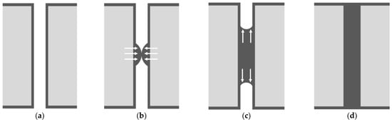
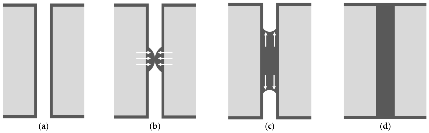
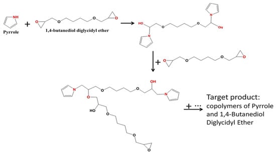
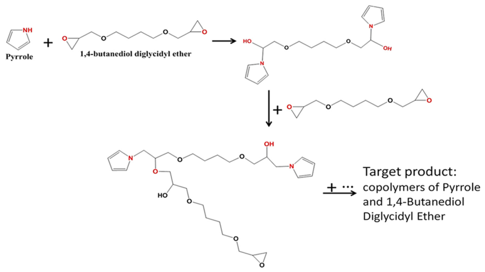
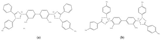
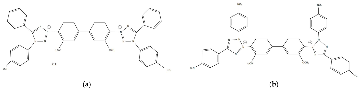
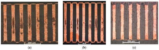
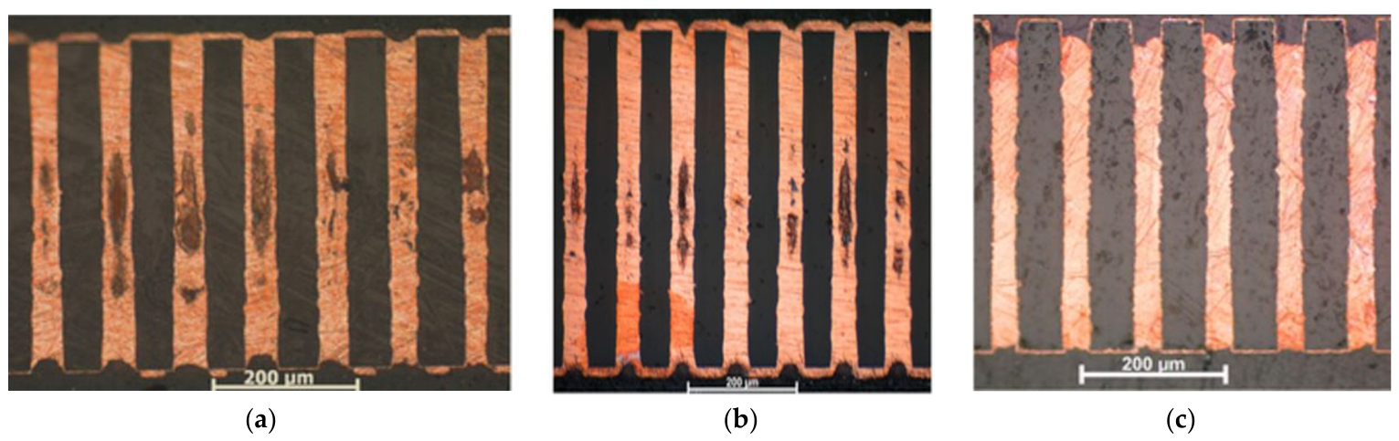
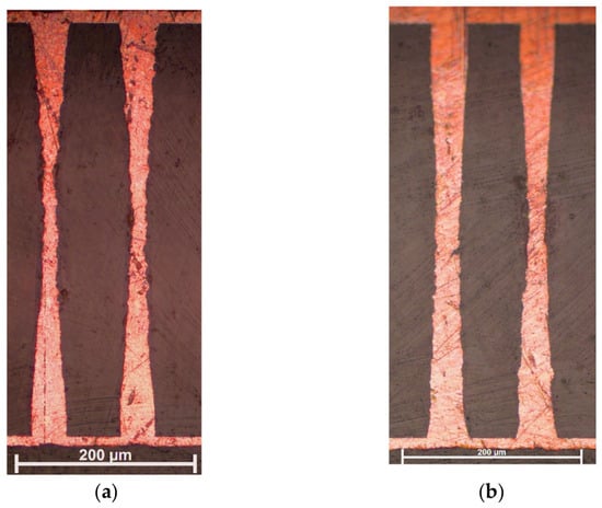
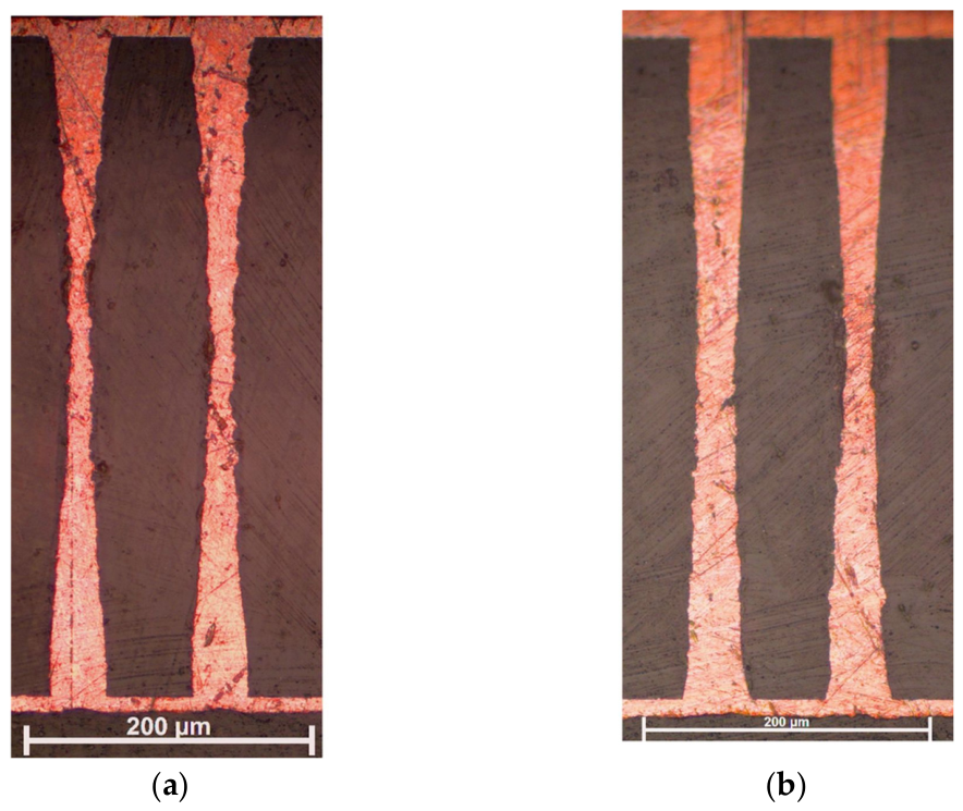
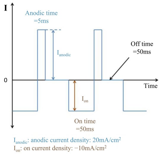
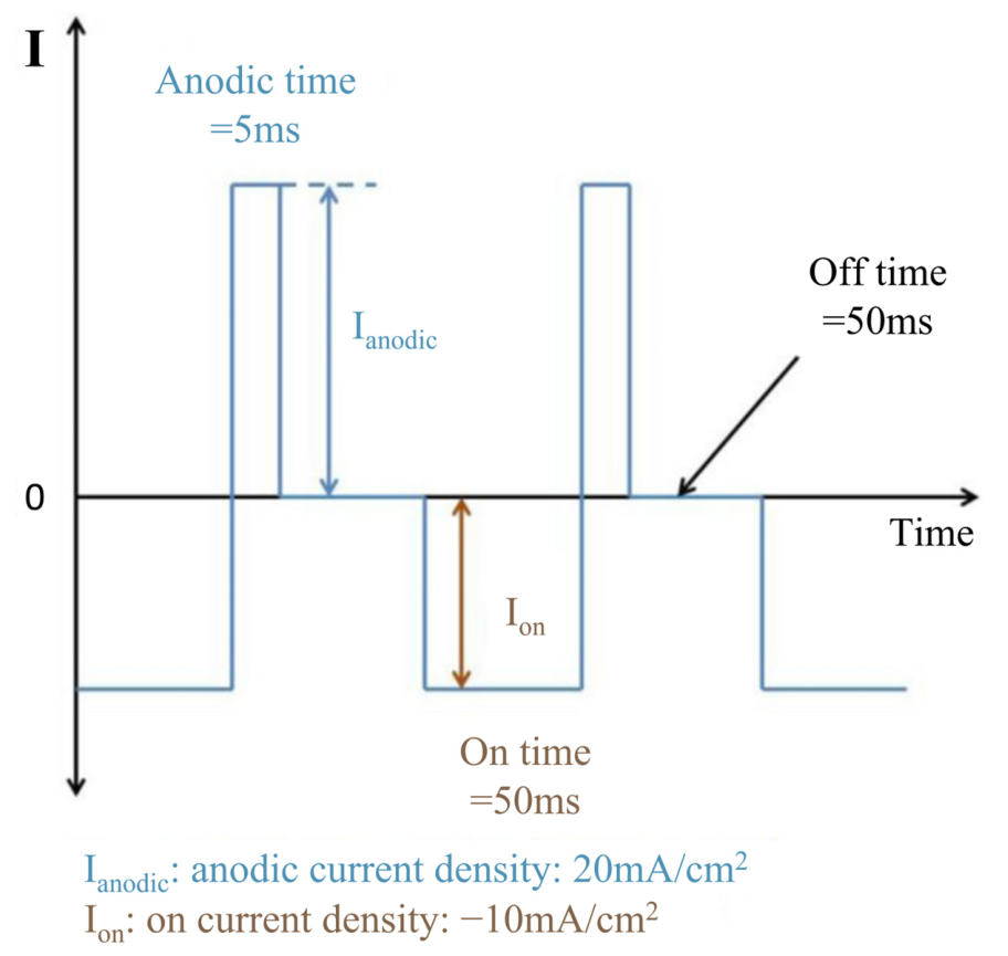
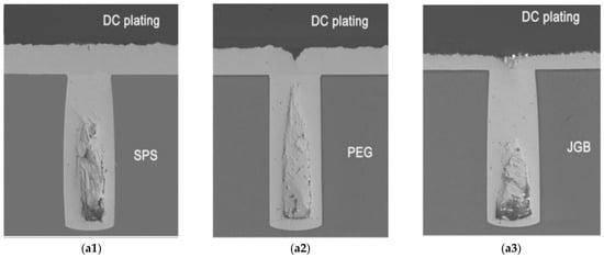
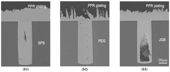
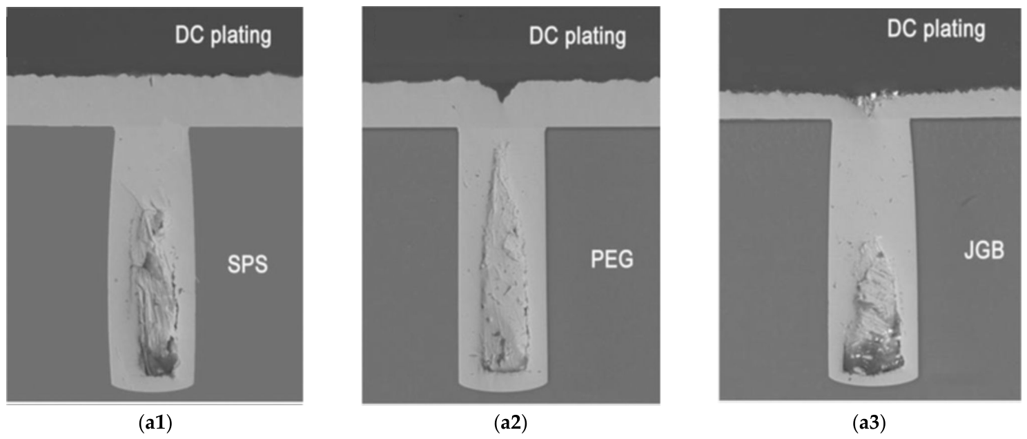
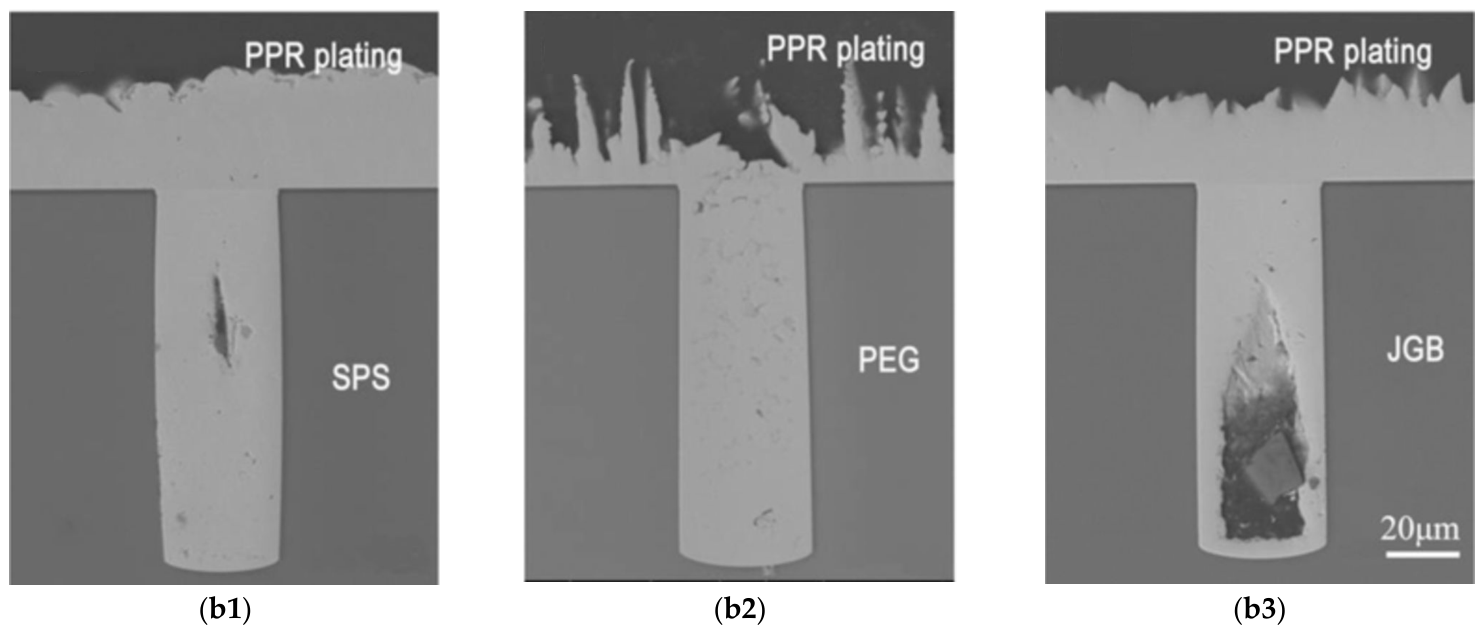
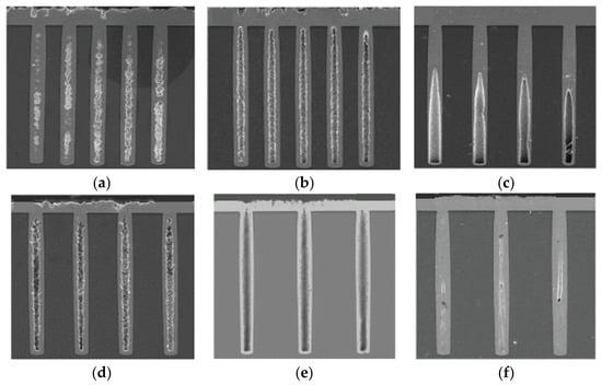
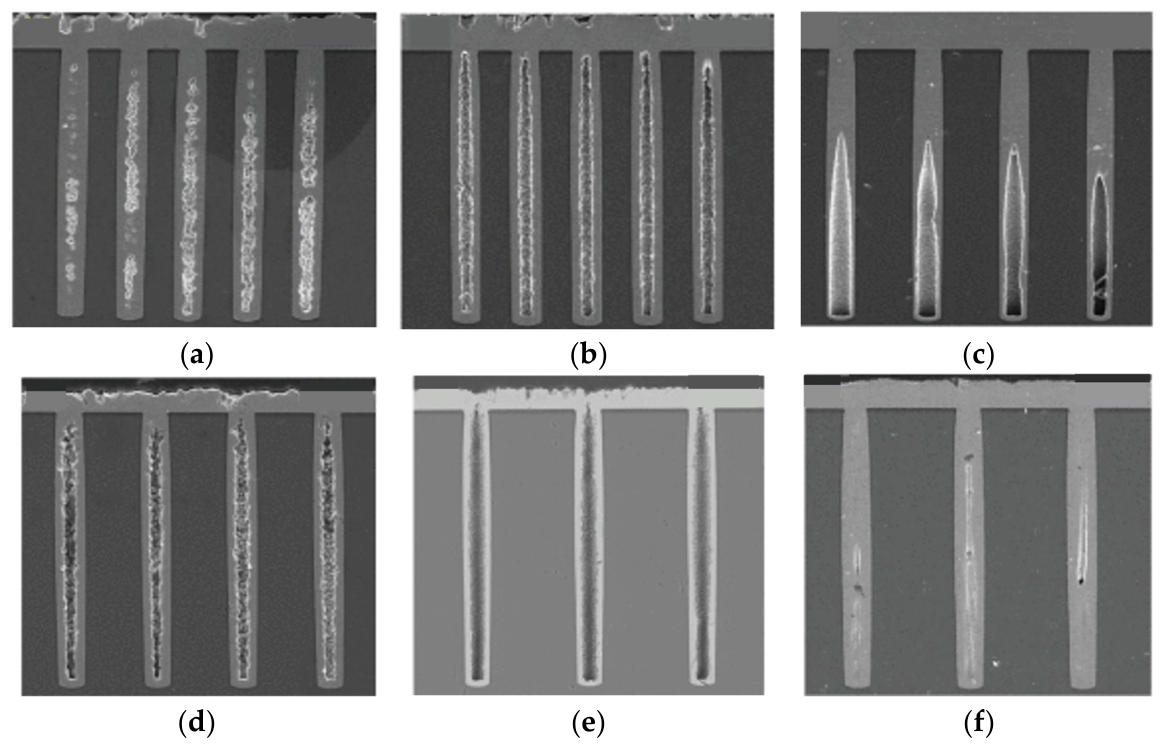
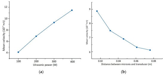
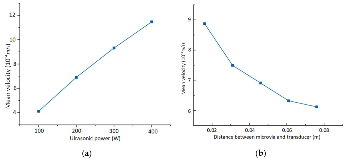
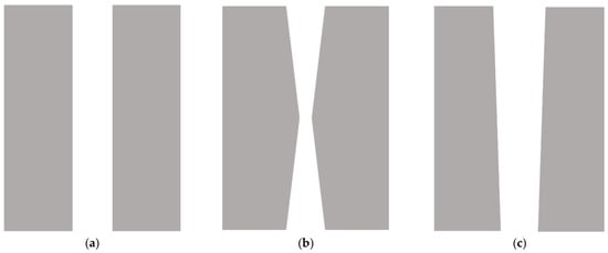
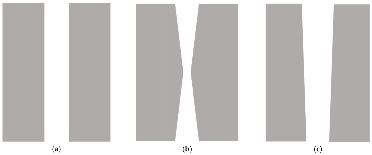
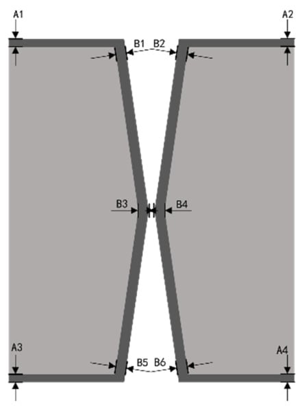
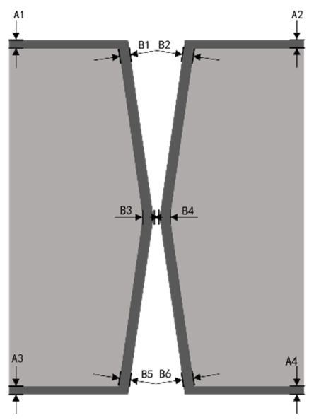
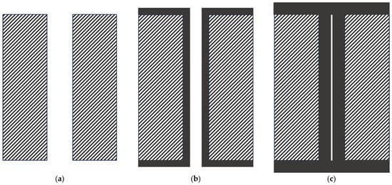
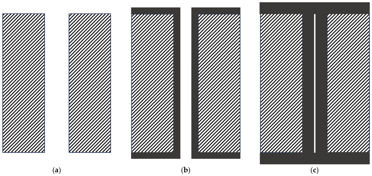
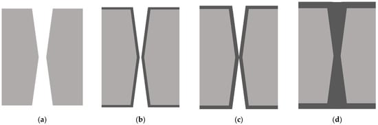
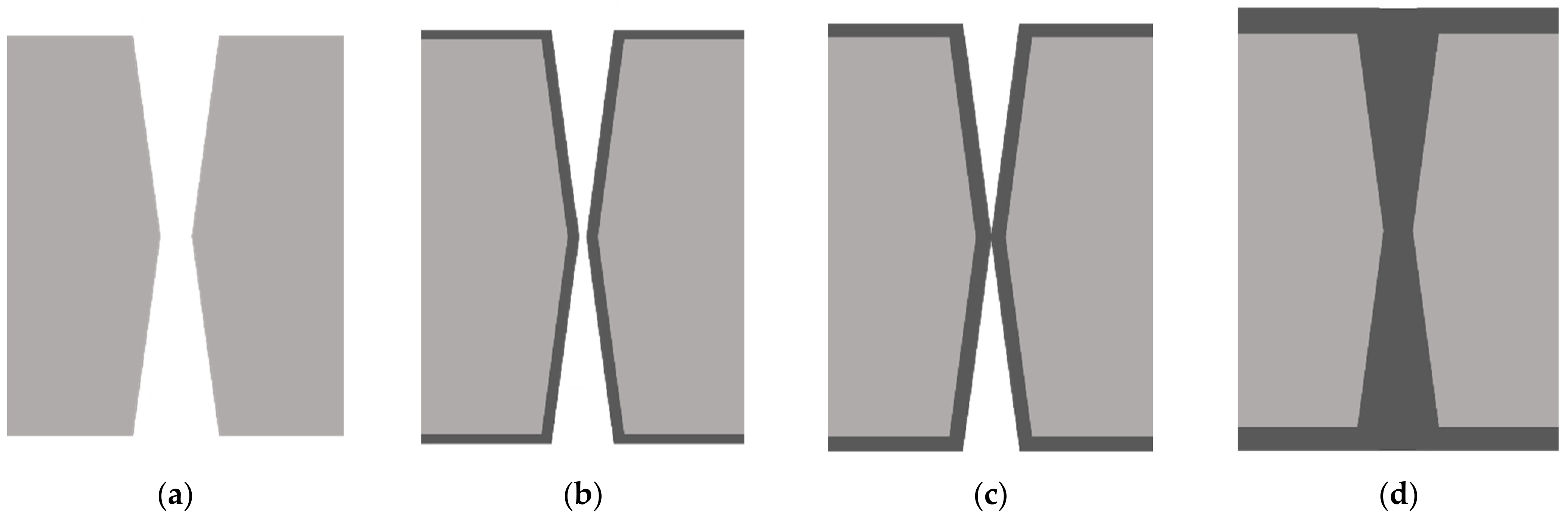

Disclaimer/Publisher’s Note: The statements, opinions and data contained in all publications are solely those of the individual author(s) and contributor(s) and not of MDPI and/or the editor(s). MDPI and/or the editor(s) disclaim responsibility for any injury to people or property resulting from any ideas, methods, instructions or products referred to in the content. |
© 2026 by the authors. Licensee MDPI, Basel, Switzerland. This article is an open access article distributed under the terms and conditions of the Creative Commons Attribution (CC BY) license.