


Abstract
The increasing adoption of 800 V-class electric vehicles has created strong demand for single-stage onboard chargers capable of operating over a wide output voltage range while maintaining high efficiency and power density. This paper presents the design and multi-objective optimization of a single-stage bidirectional AC-DC converter that integrates a three-phase interleaved totem-pole front-end with an asymmetric CLLC resonant converter. The proposed topology eliminates large electrolytic DC-bus capacitors by using only small film capacitors and enables seamless operation across an ultra-wide battery voltage range of 100–850 V. The asymmetric CLLC parameters were optimized using a combination of fundamental harmonic approximation (FHA), time-domain analysis (TDA), and multi-objective particle swarm optimization (PSO) to achieve high voltage gain, wide zero-voltage switching (ZVS), and high efficiency. Simulations show a peak efficiency of 97.1%, an input-current THD of 2.8%, primary ZVS down to about 18% load, and bidirectional (V2G) operation. The design is a candidate for 800 V-class onboard chargers that must cover 100–850 V.
1. Introduction
The adoption of 800 V-class electric vehicles has increased the need for onboard chargers with high efficiency and a wide output voltage range. Modern packs often require operation from 100 V during pre-charge to more than 850 V at full charge. This range is difficult for conventional chargers, which must keep high efficiency and soft switching over the full battery window.
Most onboard chargers still use a two-stage structure: an AC-DC power-factor-correction (PFC) stage followed by an isolated DC-DC converter [1,2,3]. This arrangement is mature, but it increases component count and conversion loss. The intermediate DC-bus also usually needs large electrolytic capacitors, which limit lifetime and power density. These drawbacks have motivated single-stage AC-DC chargers that combine PFC and isolation and can operate with a much smaller DC-bus capacitor [4,5,6].
Among isolated resonant topologies, the CLLC converter is attractive because it can achieve zero-voltage switching (ZVS) and bidirectional grid-to-vehicle (G2V) and vehicle-to-grid (V2G) operation [7,8]. Symmetric CLLC tanks, however, often cannot cover 100–850 V without a large efficiency or control penalty. Asymmetric CLLC designs improve the gain range, but most studies treat the tank as a DC-DC stage with an ideal input source. Accurate time-domain models and electrolytic-capacitor-less single-stage chargers have been reported, yet they generally separate the resonant tank from the front-end PFC, or they do not combine the 100–850 V range with a three-phase interleaved totem-pole architecture [7,9,10,11,12]. Interleaved multimode totem-pole PFC can reduce conduction loss and input ripple, but its use with an asymmetric CLLC stage under one control law is still uncommon, especially above 20 kW.
This paper presents an integrated design and multi-objective optimization framework for a 22 kW single-stage bidirectional AC-DC charger. A three-phase interleaved totem-pole front-end is combined with an asymmetric CLLC resonant stage and only small film capacitors on the DC-bus. The tank parameters are obtained using fundamental harmonic approximation (FHA), time-domain analysis (TDA), and multi-objective particle swarm optimization (PSO). The work develops a true single-stage topology for 100–850 V operation without large electrolytic bus capacitors, a systematic FHA/TDA/PSO procedure for the asymmetric resonant parameters, and a unified control strategy for multimode totem-pole operation, CLLC frequency modulation, and bidirectional power flow, which is then verified by time-domain simulation.
2. Methodology
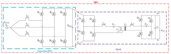
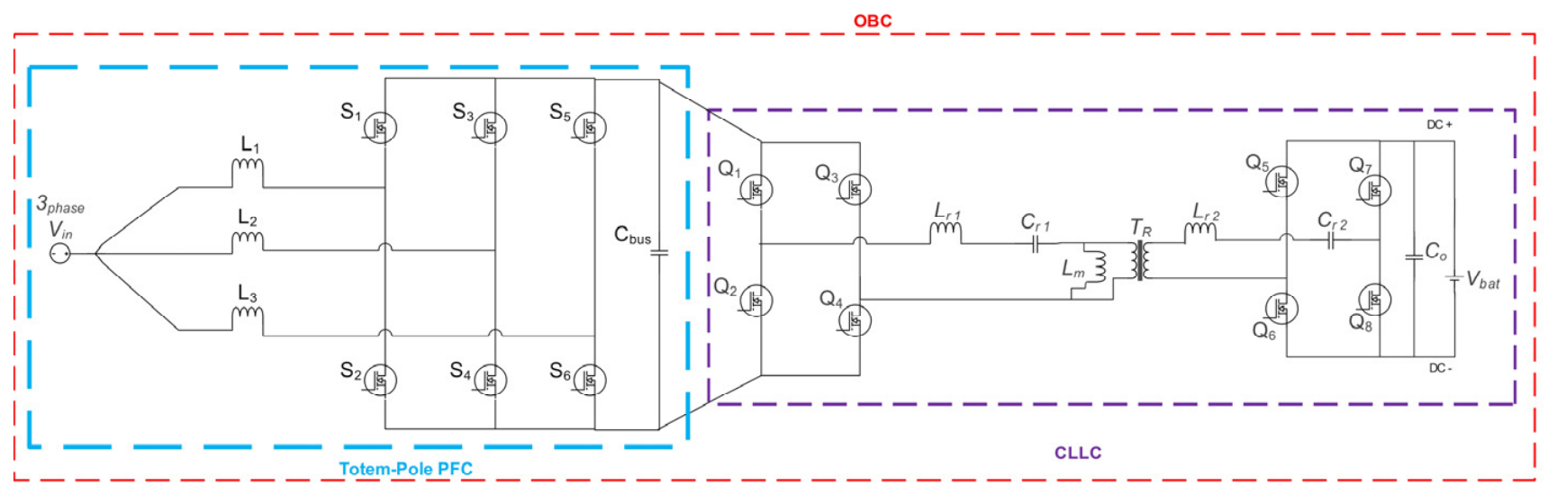
The proposed single-stage bidirectional AC-DC converter integrates a three-phase interleaved totem-pole front-end with an asymmetric CLLC resonant converter to achieve high efficiency and wide voltage regulation capability for EV charging applications. The overall system configuration is illustrated in Figure 1. The topology is designed to operate with small film capacitors at the DC bus, eliminating the need for large electrolytic capacitors commonly used in conventional chargers [13,14]. This approach improves power density, reliability, and lifetime while maintaining the ability to regulate the output voltage from 100 V to 850 V.
Figure 1.
Proposed single-stage topology: three-phase interleaved totem-pole front-end and asymmetric CLLC stage.
The complete design specifications of the proposed 22 kW single-stage converter, including power rating, voltage ranges, semiconductor devices, and all key passive components, are summarized in Table 1.
Table 1.
Complete design specifications of the proposed 22 kW single-stage converter.
The conduction and switching-loss estimates, as well as the ZVS-boundary calculation, use the approximate device parameters listed in Table 1: and for the primary-side 650 V GaN devices, and and for the secondary-side 1200 V SiC devices. These values are modeling assumptions corresponding to typical 650 V GaN and 1200 V SiC devices at 125 °C and are not tied to a particular commercial part number.
As shown in Figure 1, the converter consists of two main power stages. The front-end stage employs a three-phase interleaved totem-pole bridgeless boost converter. Each phase leg comprises two GaN or SiC MOSFETs operating in a totem-pole configuration. Interleaving the three phases at 120° phase shift significantly reduces the input current ripple and allows the use of smaller boost inductors. The multimode operation of the totem-pole stage enables the converter to function in both continuous conduction mode (CCM) and triangular conduction mode (TCM) depending on the load and grid conditions, thereby optimizing efficiency across a wide power range.
The isolated DC-DC stage is realized using an asymmetric CLLC resonant converter. Unlike conventional symmetric CLLC designs where the resonant parameters on both sides of the transformer are identical, the proposed converter uses different values for the primary and secondary resonant inductors and capacitors. This asymmetry is intentionally introduced to extend the voltage gain range while maintaining zero-voltage switching (ZVS) on both the primary and secondary switches. The transformer turns ratio is selected as 0.7 to match the wide battery voltage range with the available DC-bus voltage. The magnetizing inductance is designed to provide sufficient energy for ZVS commutation while limiting the circulating current.
One of the key features of the proposed topology is the use of small film capacitors at the DC bus instead of large electrolytic capacitors. In the proposed design, only small film capacitors with a total capacitance of 50 µF and a voltage rating of 700 V are used at the intermediate DC-bus. Because the totem-pole front-end operates in an interleaved manner and the CLLC stage provides a degree of voltage regulation through frequency modulation, the DC-bus voltage ripple can be managed without requiring large capacitance. This reduces the required DC-bus capacitance and removes the lifetime limitation associated with electrolytic capacitors.
Compared with conventional two-stage onboard chargers, the proposed converter uses a single power stage and only small film capacitors on the DC-bus, which removes the large electrolytic bank required by most two-stage designs [1,2,3]. Symmetric CLLC and other single-stage chargers can reach high efficiency, but they usually cover a narrower battery window than 100–850 V [5,7,9,11]. A detailed quantitative comparison with recently reported chargers is given in Section 3. The present design therefore targets the combination of single-stage conversion, an asymmetric CLLC tank, and electrolytic-capacitor-free 100–850 V operation.
The design methodology of the proposed converter consists of several interrelated steps. First, the FHA technique is employed to derive the voltage gain characteristics of the asymmetric CLLC tank. This analytical model allows rapid evaluation of the converter behavior across different operating frequencies and load conditions. Second, time-domain analysis is performed to accurately capture the ZVS conditions of both primary and secondary switches, taking into account the nonlinear output capacitance of the MOSFETs and the reverse recovery charge of the body diodes. Third, a multi-objective particle swarm optimization (PSO) algorithm is applied to determine the optimal values of the resonant components (, , , ) and the magnetizing inductance . The optimization objectives include achieving the required voltage gain, ensuring ZVS operation over a wide load range, and maximizing efficiency at the nominal operating point.
Following the parameter optimization, the control strategy is developed. The interleaved totem-pole front-end is controlled using sinusoidal pulse-width modulation (SPWM) with phase-shift interleaving to achieve high power factor and low input current distortion. The asymmetric CLLC stage is regulated using pulse-frequency modulation (PFM), where the switching frequency is varied to control the power flow and output voltage. A mode selection mechanism is implemented to transition between different operating modes depending on the battery voltage and power demand. Detailed descriptions of the FHA modeling, optimization process, and control implementation are provided in the following subsections.
2.1. Fundamental Harmonic Approximation Modeling
The main symbols used in the modeling and optimization of the proposed converter are listed in Table 2.
Table 2.
Nomenclature used in this paper.
The fundamental harmonic approximation (FHA) technique is widely used in the analysis and design of resonant converters due to its simplicity and reasonable accuracy under sinusoidal current assumptions. In this work, FHA is employed as the first step to derive the voltage gain characteristics of the asymmetric CLLC resonant tank and to provide initial design guidelines before performing time-domain analysis and optimization.
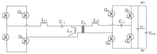
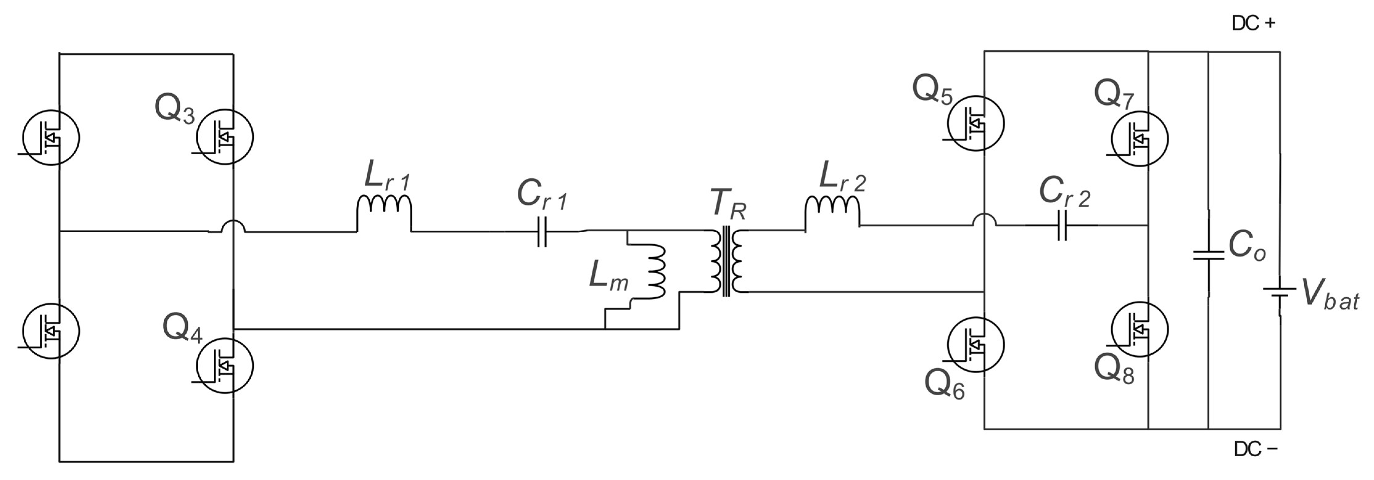
Figure 2 shows the AC equivalent circuit of the proposed asymmetric CLLC converter under FHA. The square-wave voltages generated by the primary and secondary full-bridge switches are approximated by their fundamental components. The transformer is modeled with its magnetizing inductance and an ideal transformer with turns ratio . The primary resonant tank consists of and , while the secondary resonant tank consists of and . Because the resonant parameters on both sides are different, the circuit is inherently asymmetric, which provides greater design flexibility for wide voltage gain applications.
Figure 2.
AC equivalent circuit of the asymmetric CLLC tank used for FHA sizing.
To facilitate analysis, all secondary-side components are reflected to the primary side. The reflected secondary resonant inductance and capacitance are given by and , respectively. The equivalent load resistance referred to the primary side is expressed as , where is the equivalent load resistance at the battery side. The primary resonant frequency of the asymmetric CLLC tank is given by:
The normalized switching frequency is defined as:
The quality factor and the inductance ratio are expressed as:
The voltage gain of the CLLC converter is defined as:
FHA is used only for initial sizing. The printed gain formula of a symmetric LLC tank is not used as the design equation. All reported voltage-gain curves come from time-domain simulation.
It should be noted that the FHA model is a simplified representation used primarily for initial parameter selection and for obtaining qualitative insight into the voltage gain characteristics. Because of the strong asymmetry between the primary and secondary resonant tanks, the accuracy of FHA decreases at frequencies far from resonance and under light-load conditions. Therefore, all final voltage-gain curves, ZVS boundaries, and efficiency results reported in this paper are obtained from detailed time-domain simulations. A more accurate time-domain analysis of asymmetrical CLLC converters can be found in [7].
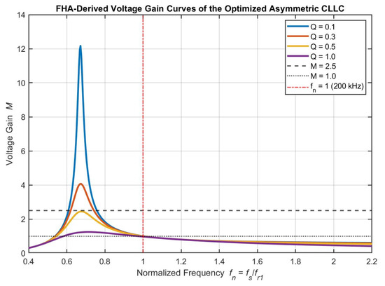
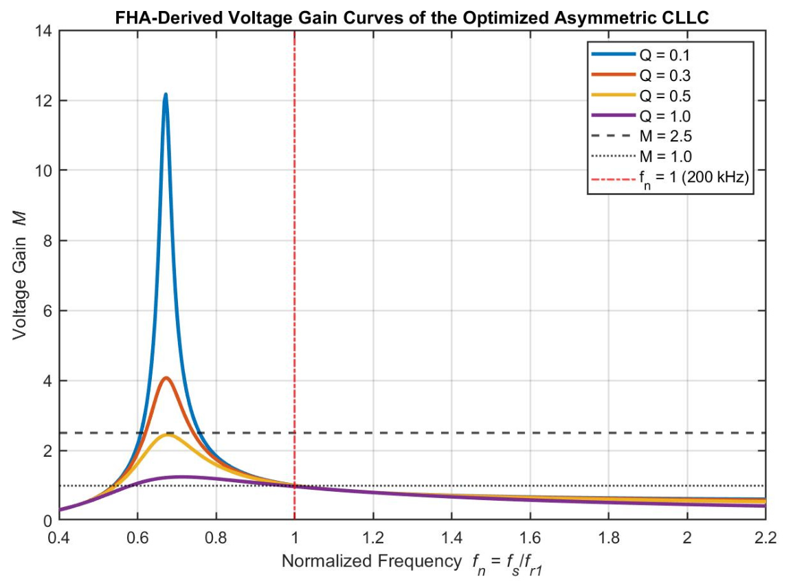
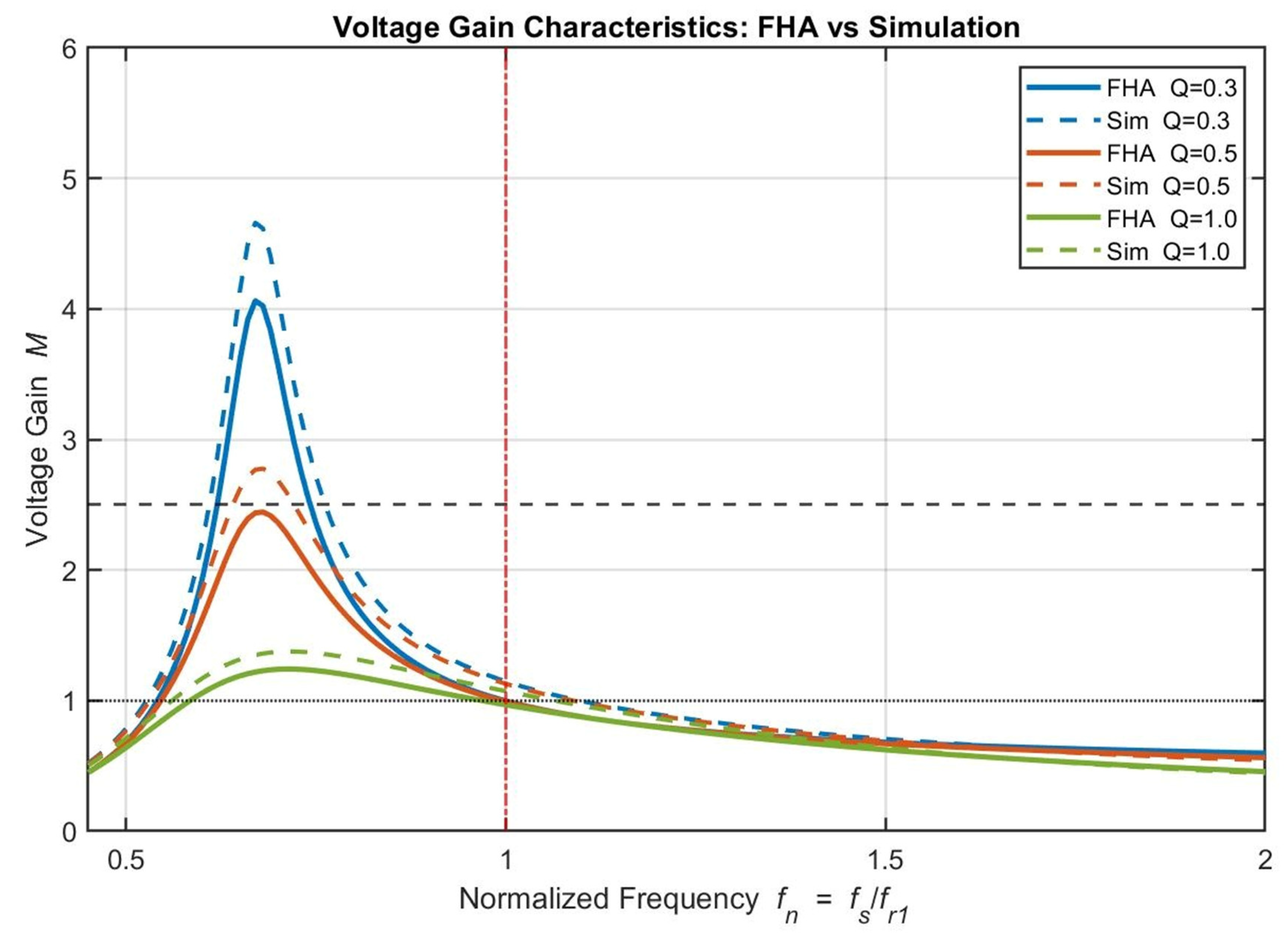
The FHA-derived voltage gain curves for different quality factors are shown in Figure 3. These curves illustrate the wide gain capability of the optimized asymmetric CLLC tank and serve as the basis for selecting the nominal operating frequency and the frequency modulation range. As observed, the converter can achieve voltage gains greater than 2.5 for light-to-medium loads at normalized frequencies below 0.8, while the gain remains close to unity near the nominal frequency of 200 kHz. This behavior is essential for covering the ultra-wide battery voltage range of 100–850 V without requiring an excessively high transformer turns ratio.
Figure 3.
FHA voltage gain curves of the optimized asymmetric CLLC for , , , and . Gains exceed 2.5 at and remain close to unity near 200 kHz.
It should be noted that the accuracy of the FHA model decreases at very light load conditions and at operating frequencies far from resonance, where the current waveforms become less sinusoidal. Nevertheless, the FHA approach remains a useful and computationally efficient tool for the preliminary design and parameter selection of the asymmetric CLLC converter. The parameters obtained from FHA analysis are subsequently refined through time-domain analysis and multi-objective PSO optimization, as described in the following subsections.
2.2. Optimization Procedure Using Particle Swarm Optimization
The design of the asymmetric CLLC resonant converter involves multiple conflicting objectives, including achieving the required voltage gain over a wide output voltage range, ensuring zero-voltage switching (ZVS) operation across a broad load range, and maximizing efficiency while keeping component stresses within acceptable limits. These objectives cannot be easily satisfied through manual tuning or single-objective optimization methods. Therefore, a multi-objective particle swarm optimization (PSO) algorithm is employed to determine the optimal values of the resonant parameters.
The PSO algorithm is chosen for its simplicity, fast convergence, and proven effectiveness in power electronics optimization problems. In this work, the PSO is implemented with a swarm size of 50 particles and a maximum of 200 iterations. The inertia weight is linearly decreased from 0.9 to 0.4 over the iterations to balance exploration and exploitation. The cognitive and social acceleration coefficients are set to 1.5 and 2.0, respectively.
The optimization variables include the primary and secondary resonant inductors (, ), resonant capacitors (, ), and the magnetizing inductance (). The transformer turns ratio is also included as an optimization variable within a constrained range to provide additional design flexibility. The nominal switching frequency is allowed to vary between 150 kHz and 250 kHz.
Three main objective functions are defined. The first objective is to minimize the deviation from the target voltage gain across the full output voltage range (100–850 V) at different load conditions. The second objective is to maximize the ZVS margin on both the primary and secondary sides by ensuring sufficient magnetizing current and minimizing the turn-off current of the switches. The third objective is to maximize the converter efficiency at the nominal operating point by reducing conduction and switching losses. These objectives are combined into a single fitness function using a weighted sum approach, where the weights are selected based on the relative importance of each objective for EV charging applications.
The multi-objective fitness function used in the PSO algorithm is defined as:
In the multi-objective PSO, each particle is evaluated using the fitness function defined in Equation (5). The four terms are obtained as follows: the conduction and switching loss term () is estimated from a simplified time-domain model that accounts for device and the resonant current waveform; the ZVS margin is calculated analytically from the magnetizing current and the required charge to discharge the switch output capacitance; the output voltage ripple and input current THD are obtained from fast time-domain simulations of the complete converter. The weighting factors used in this work are (losses), (ZVS margin), (ripple), and (THD). These weights were selected to prioritize efficiency and soft-switching while still maintaining acceptable ripple and current quality.
These weights reflect the priority of a wide-range EV charger: efficiency and ZVS decide whether the converter is acceptable, so they receive the two largest coefficients. Ripple and THD are already constrained by three-phase interleaving and the 50 µF film bus; they remain in the fitness with smaller weights so that a low-loss particle is rejected if current quality or bus ripple becomes poor. The 100–850 V gain window, inductive-region operation, and device stress limits are enforced as penalties and do not depend on –. A separate optimization for other weight combinations was not carried out.
Several constraints are imposed during the optimization process. The maximum current through the resonant inductors and the maximum voltage across the resonant capacitors are limited to avoid excessive component stress. The switching frequency is constrained to remain above the primary resonant frequency to ensure operation in the inductive region, which is necessary for achieving ZVS. In addition, the quality factor and inductance ratios are monitored to prevent operation in regions where the gain curve becomes highly sensitive to parameter variations.
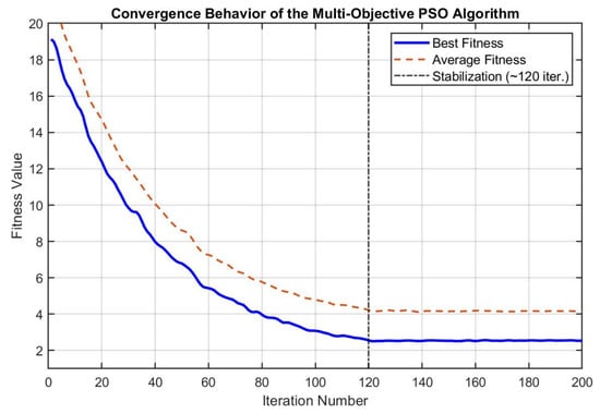
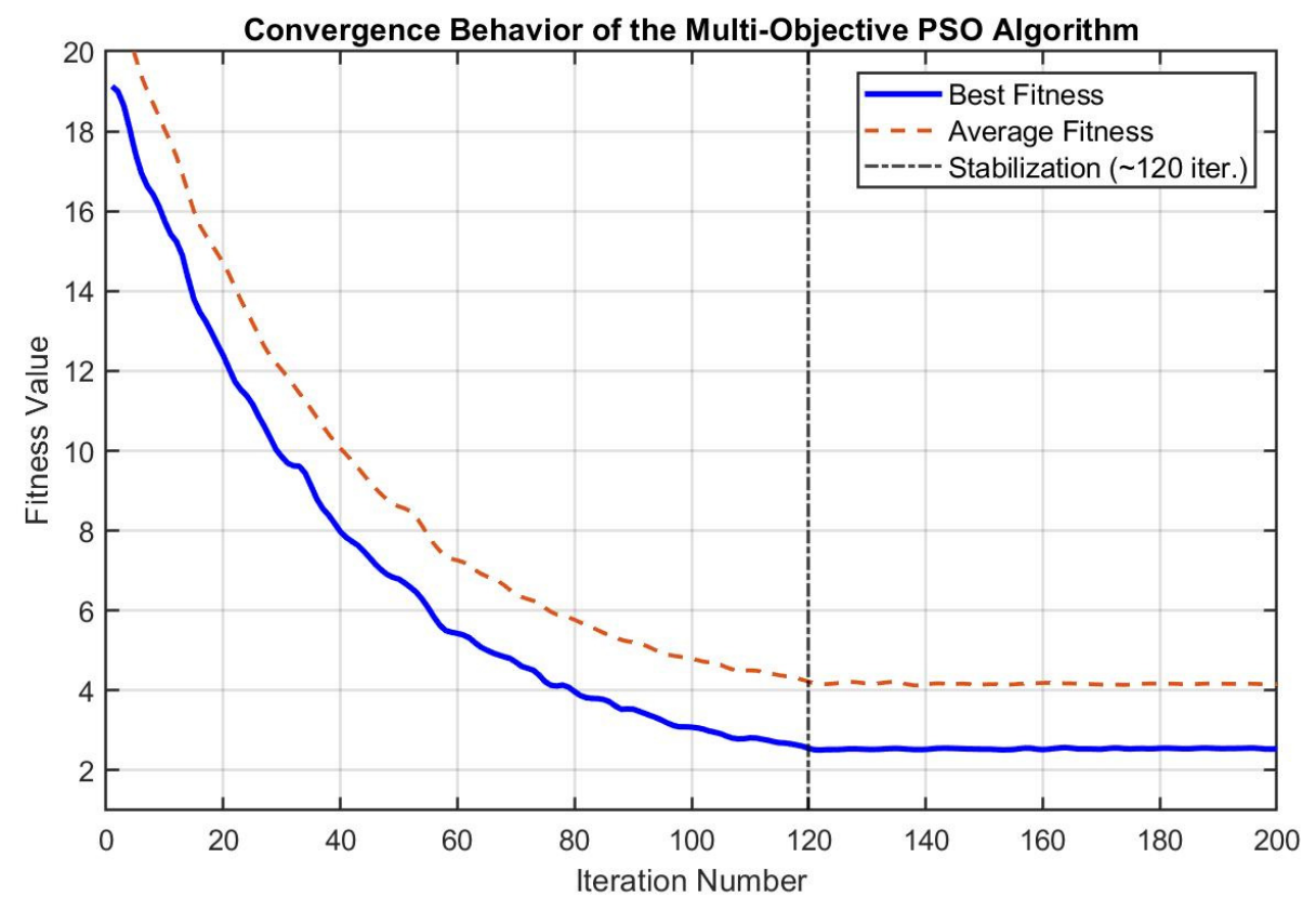
The PSO algorithm evaluates the fitness of each particle by first calculating the FHA voltage gain and then performing a simplified time-domain analysis to verify ZVS conditions. Particles that violate any of the defined constraints are penalized by assigning them a significantly worse fitness value. After the optimization process converges, the best particle is selected as the optimal design. The convergence behavior of the PSO algorithm is illustrated in Figure 4, where the fitness value stabilizes after approximately 120 iterations.
Figure 4.
Convergence behavior of the multi-objective PSO algorithm. The best fitness value stabilizes after approximately 120 iterations.
The optimized parameters obtained from the PSO are summarized in Table 3. Compared with the initial design values derived from conventional FHA calculations, the optimized parameters provide a better trade-off between voltage gain capability, ZVS range, and efficiency by increasing the degree of asymmetry in the resonant tank.
Table 3.
Optimized resonant tank parameters obtained from the multi-objective PSO algorithm compared with the initial design values.
In particular, the asymmetry between the primary and secondary resonant tanks is increased, allowing the converter to achieve higher gain at lower switching frequencies while maintaining ZVS operation down to 18% of the rated load across the entire voltage range.
Reducing from 66 µH to 22 µH increases the magnetizing current and therefore the ZVS energy (), which keeps primary ZVS down to about 18% load. The same current increases circulating conduction loss. PSO selected 22 µH as the compromise between that ZVS margin and extra RMS current.
It should be noted that the PSO optimization is performed offline during the design stage. Once the optimal parameters are determined, they are fixed in the hardware implementation. However, the control system retains the flexibility to adjust the switching frequency in real time to regulate the output voltage and power, as described in the following subsection.
The effectiveness of the optimization is further validated through detailed time-domain simulations and efficiency analysis, which are presented in Section 3. The optimized design demonstrates that the combination of FHA modeling and PSO can effectively overcome the limitations of manual design approaches and yield a CLLC converter that meets the stringent requirements of wide voltage range single-stage EV charging applications.
2.3. Control Strategy
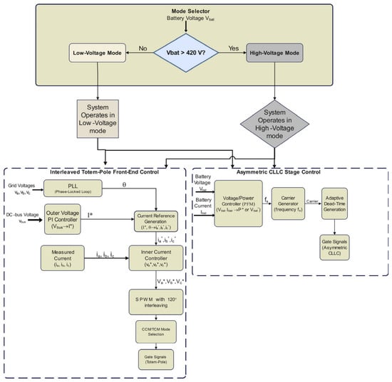
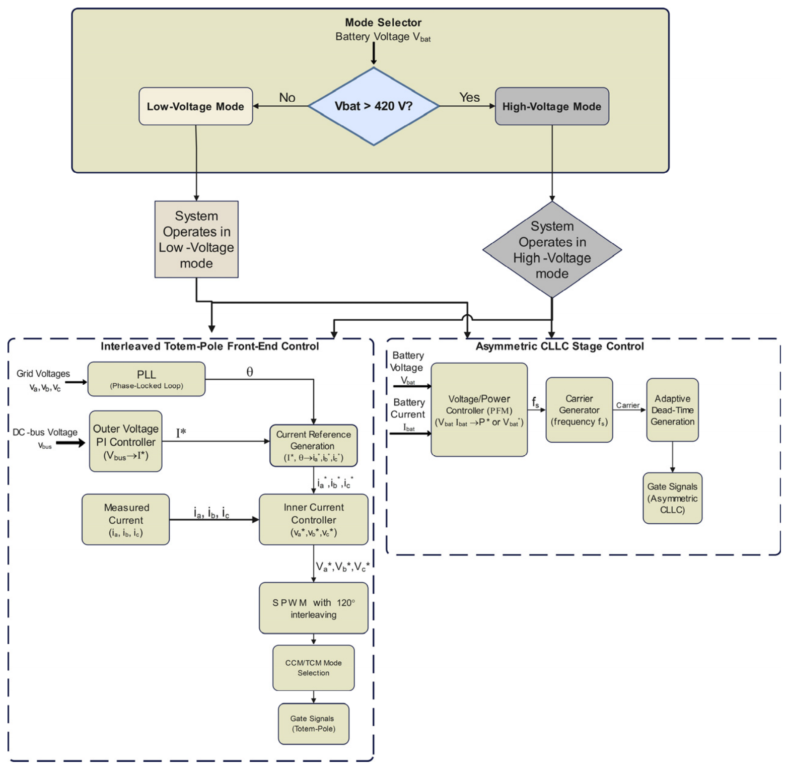
The control system of the proposed single-stage converter is designed to achieve high power factor, low input current distortion, wide output voltage regulation, and soft-switching operation across the full load and voltage range. The control architecture consists of two coordinated parts: the front-end interleaved totem-pole control and the asymmetric CLLC stage control, as illustrated in the control block diagram shown in Figure 5.
Figure 5.
Control block diagram of the proposed single-stage converter with mode selection, interleaved totem-pole control, and asymmetric CLLC PFM control.
The three-phase interleaved totem-pole front-end is controlled using sinusoidal pulse-width modulation (SPWM) with a 120° phase shift between the three phases. This interleaving significantly reduces the input current ripple and allows the use of smaller boost inductors. A conventional dual-loop control structure is employed, consisting of an outer voltage loop that regulates the DC-bus voltage and an inner current loop that shapes the input currents to be sinusoidal and in phase with the grid voltages. The current references for each phase are generated from the measured grid voltages using a phase-locked loop (PLL). To improve efficiency at light load, a mode selection block dynamically switches between continuous conduction mode (CCM) and triangular conduction mode (TCM) based on the instantaneous load current. CCM is used above 22% load and TCM below 18% load, with a 4% hysteresis band around the 20% threshold to avoid chattering. In the simulation the next TCM pulse is triggered by inductor-current ZCD on , and . Device voltage valley sensing is an equivalent hardware option and is not used in the reported simulations. In CCM the same current loop runs 120° interleaved SPWM and ZCD is not used to start the pulse.
The outer voltage loop of the totem-pole stage is designed with a bandwidth of approximately 15 Hz, while the inner current loop has a bandwidth of about 1.2 kHz. The control algorithm is executed at a sampling frequency of 40 kHz. Adaptive dead-time is calculated in real time according to the instantaneous resonant current and the switch output capacitance, ensuring sufficient margin for ZVS under varying load conditions. The mode transition between Low-Voltage Mode and High-Voltage Mode is governed by a simple threshold: if the measured battery voltage , the converter operates in Low-Voltage Mode (high gain region) otherwise, it switches to High-Voltage Mode (near-resonance region).
For the asymmetric CLLC resonant stage, pulse-frequency modulation (PFM) is adopted as the primary control method. The switching frequency of the CLLC full-bridge is varied to regulate the output voltage and power flow. A lower switching frequency is used to achieve higher voltage gain when the battery voltage is low, while the frequency is increased when the battery voltage approaches its nominal value. This variable-frequency operation allows the converter to cover the wide output voltage range of 100–850 V without requiring an excessively high transformer turns ratio.
A mode selection logic is implemented to coordinate the operation of the totem-pole front-end and the CLLC stage. When the battery voltage is below 420 V, the converter operates in low-voltage mode, where the totem-pole stage maintains a relatively low DC-bus voltage and the CLLC stage operates at lower switching frequencies to provide high voltage gain. When the battery voltage exceeds this threshold, the converter switches to high-voltage mode, in which the DC-bus voltage is regulated at a higher level and the CLLC stage operates closer to its nominal frequency. This mode transition ensures that the CLLC converter always operates in a region where both high efficiency and ZVS can be maintained.
To ensure reliable ZVS operation under varying load and frequency conditions, an adaptive dead-time control scheme is applied to both the totem-pole and CLLC stages. The dead time is adjusted in real time based on the measured load current and the operating frequency. This approach minimizes body-diode conduction loss while guaranteeing ZVS turn-on of all switches.
The overall control is implemented using a digital signal processor (DSP). All feedback signals, including grid voltages, input currents, DC-bus voltage, output voltage, and battery current, are sampled and processed in the DSP. The control algorithm executes the mode selection, SPWM generation for the totem-pole stage, and frequency modulation for the CLLC stage within each switching period. Protection functions, such as overcurrent, overvoltage, and overtemperature protection, are also integrated into the control software.
The proposed control strategy enables seamless transition between different operating modes while maintaining high power quality at the grid side and high efficiency across the entire operating range. Detailed simulation results demonstrating the performance of the control system under steady-state and transient conditions are presented and discussed in Section 3.
3. Simulation and Analysis
To validate the effectiveness of the proposed single-stage asymmetric CLLC converter with interleaved totem-pole front-end, extensive time-domain simulations were carried out in MATLABR2021b /Simulink. The optimized parameters obtained from the PSO algorithm were implemented in the simulation model. The converter was tested under various operating conditions, including different battery voltages (100–850 V), load levels (20–100%), and both G2V and V2G power flow directions. The simulation results are presented and discussed in the following subsections.
3.1. Steady-State Operation and Voltage Gain Performance
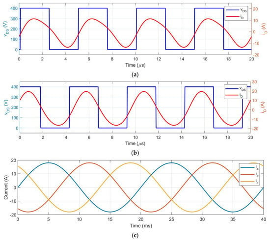
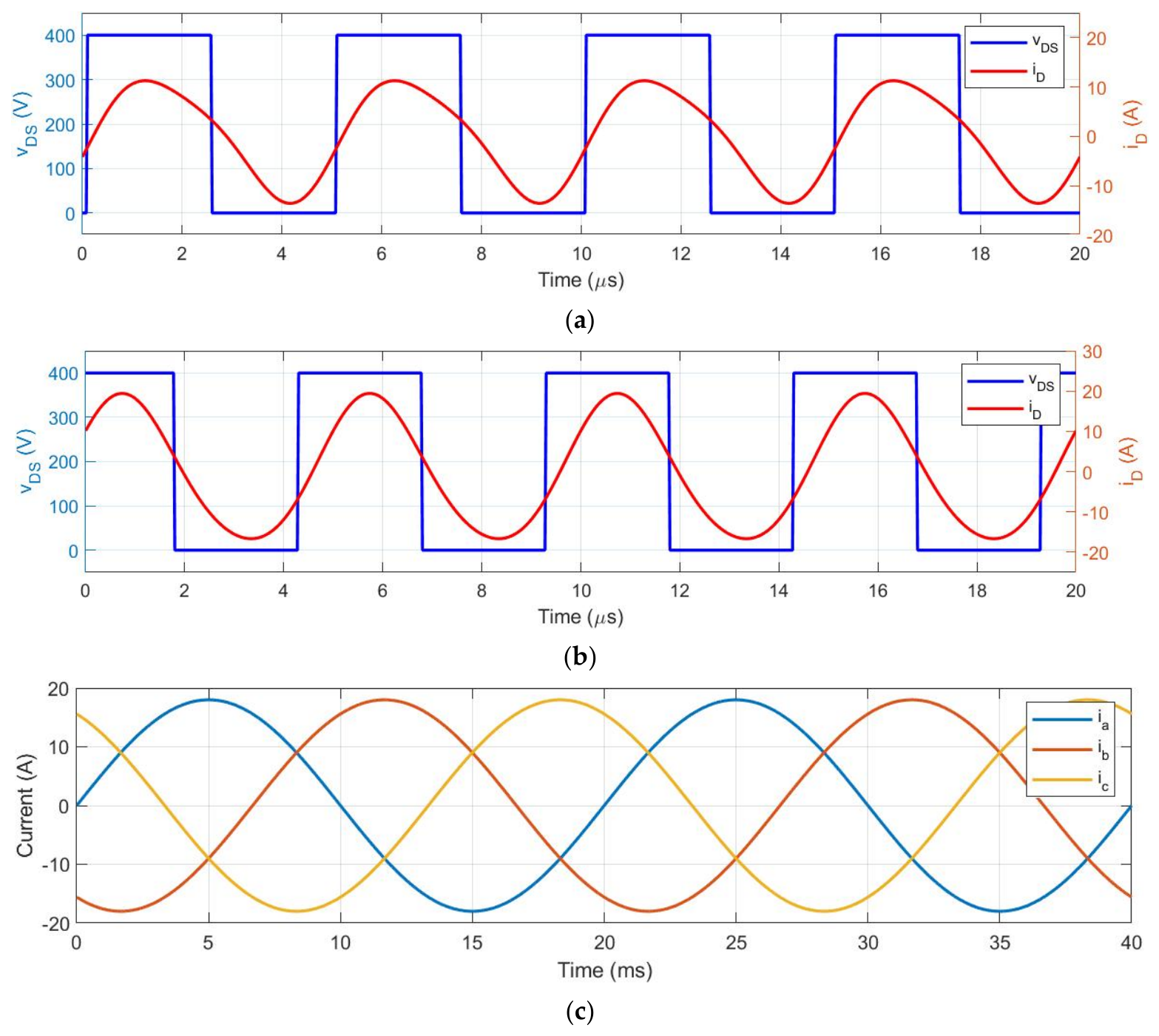
The steady-state operation of the converter was first evaluated at different output voltage levels. Figure 6 shows the key voltage and current waveforms when the converter operates at an output voltage of 400 V and delivers 50% of the rated power. The primary-side switches of the CLLC stage achieve ZVS turn-on, as indicated by the negative current flowing through the body diode before the gate signal is applied. Similarly, the secondary-side switches also operate under ZVS conditions. The input currents are sinusoidal and well balanced among the three phases, demonstrating the effectiveness of the interleaved totem-pole front-end and its control strategy.
Figure 6.
Steady-state waveforms at 400 V output and 50% load. (a) Primary-side switch voltage and current showing ZVS. (b) Secondary-side switch voltage and current showing ZVS. (c) Three-phase input currents.
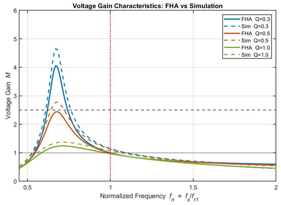
The voltage gain characteristics obtained from simulation are compared with the FHA predictions in Figure 7. The simulated gain curves follow the same trend as the FHA results in the region near the nominal operating frequency. Some deviation is observed at light load and at frequencies significantly below resonance, which is expected due to the influence of higher-order harmonics and dead-time effects not captured by the FHA model. Nevertheless, the converter successfully achieves voltage gains ranging from approximately 0.6 to above 2.8, covering the required battery voltage range of 100–850 V.
Figure 7.
Voltage gain characteristics of the optimized asymmetric CLLC converter. Comparison between FHA predictions (solid lines) and time-domain simulation results (dashed lines) for different quality factors.
FHA is not used as a predictor at the voltage extremes or at light load. At the two checked points the relative gain error is 12.1% at , and 12.9% at , (error defined as ). FHA only generates the initial gain map and the PSO start set. Away from resonance the time domain result is the design value. No operating point in the 100–850 V window relies on FHA alone.
3.2. Efficiency Performance
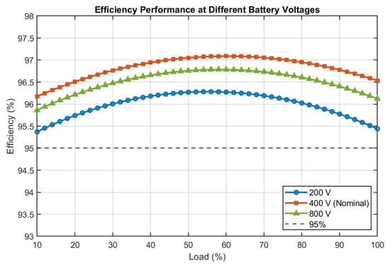
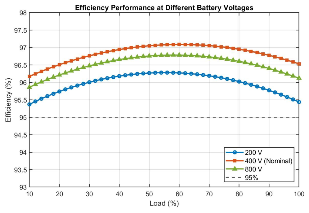
The efficiency of the proposed converter was obtained from time-domain simulations across the full output voltage and load range. Figure 8 presents the efficiency curves at three representative battery voltages: 200 V, 400 V, and 800 V. At the nominal output voltage of 400 V, the converter achieves a peak efficiency of 97.1% at approximately 60% load. Even at light load (20%), the efficiency remains above 95%, due to TCM operation of the totem-pole stage and the wide ZVS range of the CLLC stage.
Figure 8.
Efficiency curves of the proposed converter at battery voltages of 200 V, 400 V, and 800 V.
The slight reduction in efficiency at 200 V is primarily due to higher circulating current in the magnetizing inductance when the converter operates in the high-gain region. At 800 V, the switching frequency moves farther from the primary resonant frequency, increasing turn-off losses. Nevertheless, the TCM operation of the totem-pole stage at light load and the wide ZVS range of the CLLC stage keep the efficiency above 95% across the entire voltage range.
When operating at the extreme ends of the voltage range, the efficiency is slightly lower due to increased circulating current and higher switching frequency deviation from the optimal point. At 200 V output, the peak efficiency reaches 96.3%, while at 800 V output, a peak efficiency of 96.8% is obtained. These results confirm that the asymmetric CLLC design, combined with the PSO optimization, enables high efficiency across a very wide voltage range, which is one of the main advantages of the proposed topology over conventional symmetric CLLC converters.
At the nominal point (400 V, about 60% load), the loss model is dominated by conduction in the totem-pole switches and in the resonant inductors. The 97.1% peak value counts semiconductor conduction (Table 1 ), ZVS-conditioned switching loss, and resonant-inductor copper loss. Gate-drive, magnetic core, high-frequency winding, and auxiliary losses are not included as separate terms. The figure is therefore a simulation loss-model efficiency, not a measured converter efficiency. Switching loss stays low because of the wide ZVS range. The 50 µF film bus also avoids the extra ESR loss of a large electrolytic bank. This split is consistent with the efficiency curves: the dip at 200 V comes from higher circulating current, and the dip at 800 V comes from operation farther from resonance.
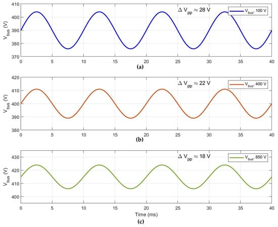
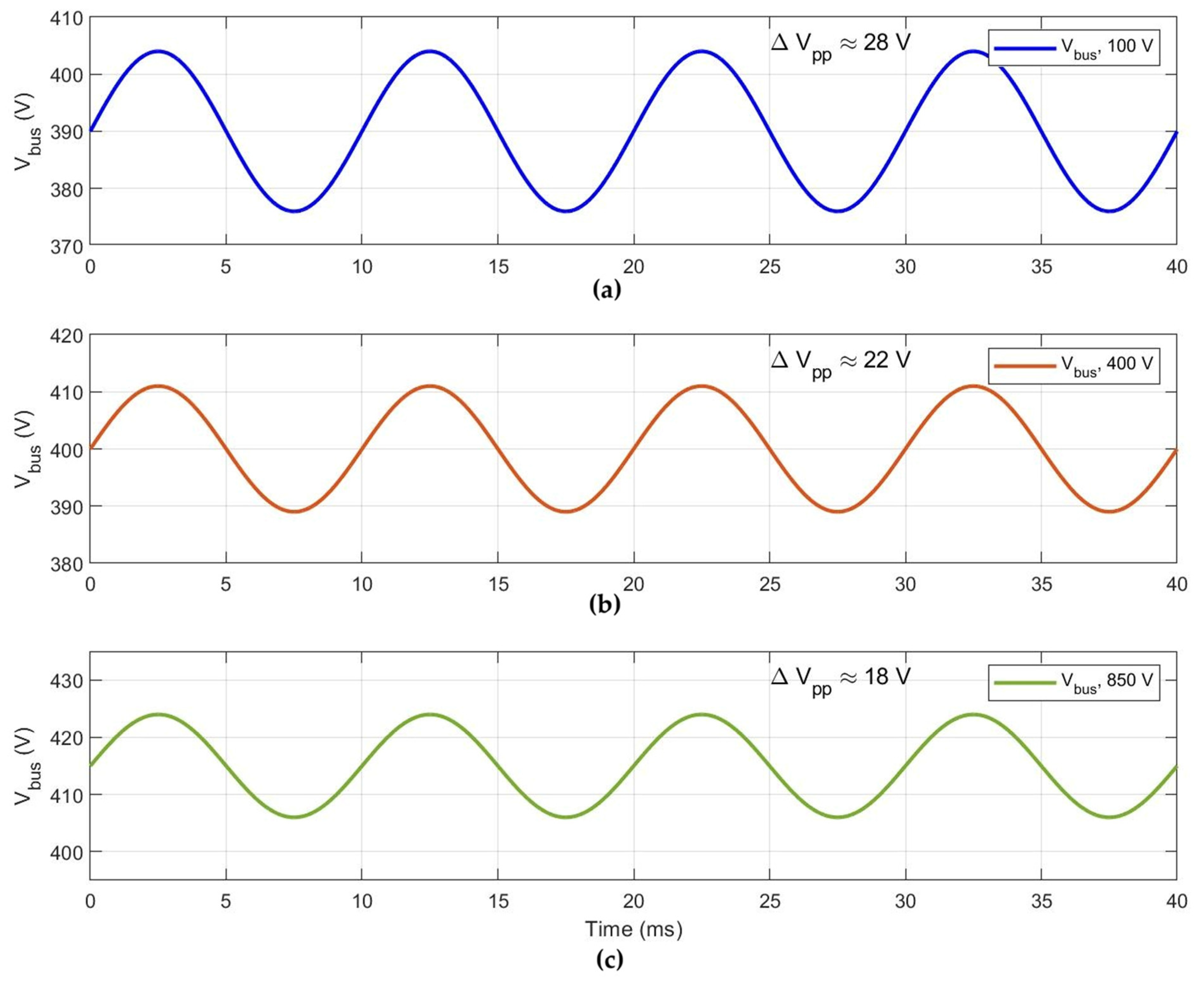
To verify the feasibility of using only small film capacitors, the DC-bus voltage ripple was examined under rated power (22 kW) at three representative battery voltages. As shown in Figure 9, the peak-to-peak ripple remains limited to approximately 28 V, 22 V, and 18 V when the battery voltage is 100 V, 400 V, and 850 V, respectively. These values correspond to less than 7.2% of the nominal DC-bus voltage. The results confirm that the combination of three-phase interleaving and frequency modulation of the asymmetric CLLC stage effectively suppresses the voltage fluctuation, allowing the use of a compact 50 µF/700 V film capacitor bank without compromising bus voltage stability. The worst-case peak-to-peak bus ripple at 22 kW is therefore 28 V, obtained at 100 V battery voltage. This value is acceptable for a 700 V film bank and is consistent with three-phase interleaving, which removes the large twice-line-frequency energy that forces electrolytic capacitors in single-phase two-stage chargers. The low-frequency RMS current associated with that 28 V/360 Hz component on 50 µF is about 1.1 A. The high-frequency RMS current of was not extracted from the switching waveforms. For a film bank the design limit in this work is the peak-to-peak voltage (28 V worst case, 700 V rating), not a tabulated HF RMS current.
Figure 9.
DC-bus voltage ripple with 50 µF film capacitor at 22 kW rated power for three battery voltages: (a) 100 V, (b) 400 V, and (c) 850 V.
The dominance of conduction losses in the totem-pole switches and resonant inductors is expected at the nominal operating point, where the converter operates near resonance and switching losses are minimized by ZVS. The relatively small contribution of the transformer and secondary-side devices indicates that the selected turns ratio and the asymmetric tank design successfully limit circulating energy. The low ESR of the film capacitors further reduces the DC-bus-related losses compared with designs that still rely on electrolytic capacitors.
3.3. ZVS Performance and Soft-Switching Range
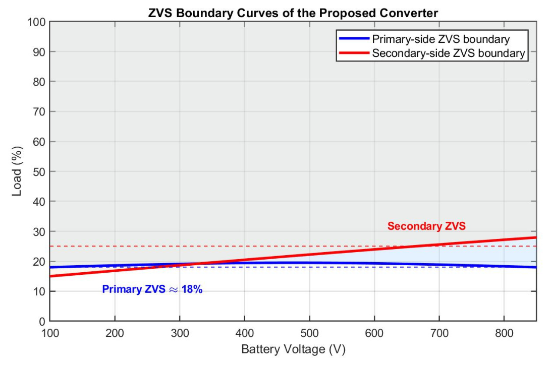
One of the key design objectives was to maintain ZVS operation over a wide load and voltage range. Figure 10 shows the ZVS boundary curves obtained from both time-domain simulation and analytical calculation. The proposed design achieves ZVS on the primary side down to approximately 18% load across the entire voltage range. On the secondary side, ZVS is maintained down to 25% load at high battery voltages and down to 15% load at low battery voltages.
Figure 10.
ZVS boundary curves of the proposed converter obtained from time-domain simulation.
The analytical ZVS test used for the primary bridge is , where and is Table 1 value. This charge balance is why the primary boundary in Figure 10 is nearly flat: depends on bus voltage and , not on load current. Raising at high battery voltage reduces and therefore the margin; the adaptive dead time is increased to keep the inequality satisfied without an unnecessarily long diode interval.
These results demonstrate that the combination of asymmetric resonant parameters and adaptive dead-time control successfully extends the soft-switching region, which is critical for maintaining high efficiency under varying EV charging conditions.
The primary-side ZVS boundary remains almost flat at approximately 18% load because the magnetizing current, which is the main source of ZVS energy, is determined by the DC-bus voltage and the magnetizing inductance, both of which are relatively constant. On the secondary side, the ZVS range becomes narrower at high battery voltages because the reflected load current decreases, reducing the energy available to discharge the switch capacitances.
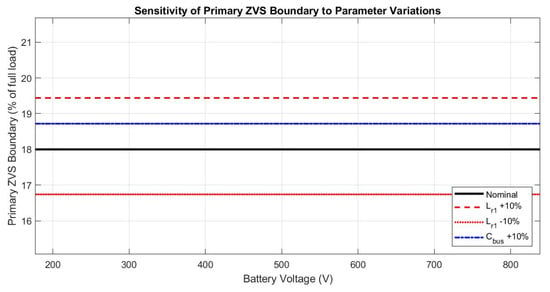
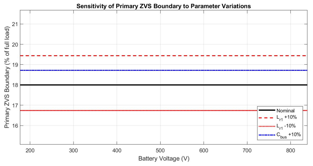
A sensitivity analysis was performed by varying the primary resonant inductance and the DC-bus film capacitance by ± 10%. As shown in Figure 11, the primary-side ZVS boundary remains between 16.7% and 19.5% of full load across the entire battery voltage range. Increasing slightly raises the minimum load required for ZVS, while decreasing improves the ZVS margin. The film capacitance variation has only a minor effect on the ZVS boundary. These results indicate that the optimized design maintains robust soft-switching performance under typical component tolerances.
Figure 11.
Sensitivity of the primary-side ZVS boundary to ±10% variation of and film capacitance .
3.4. Dynamic Response and Mode Transition
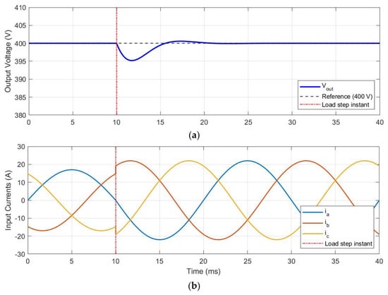
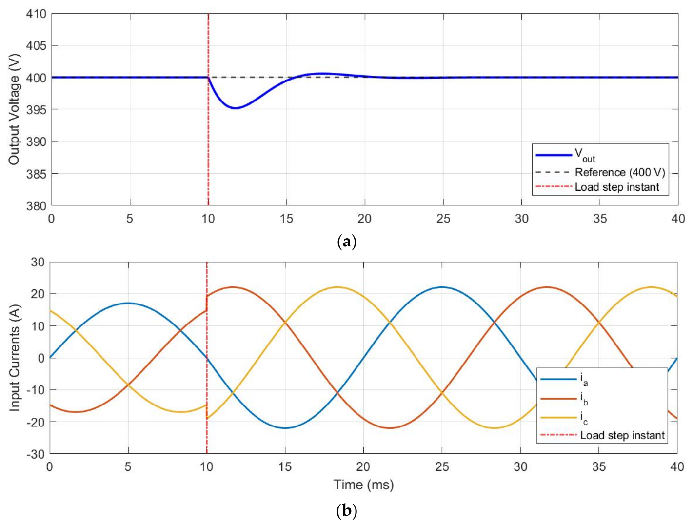
The dynamic performance of the converter was evaluated under load step changes and mode transitions. Figure 12 shows the transient response when the output power suddenly changes from 50% to 100% load at a constant battery voltage of 400 V. Subplot (Figure 12a) presents the output voltage, which recovers within approximately 7 ms with an undershoot of less than 3%. Subplot (Figure 12b) shows that the three-phase input currents remain sinusoidal and balanced throughout the transient, demonstrating good dynamic regulation capability of the control system.
Figure 12.
Dynamic response of the converter to a load step from 50% to 100% at 400 V battery voltage, (a) output voltage reponse to load step 50% to 100% and (b) three-phase input currents during the load step.
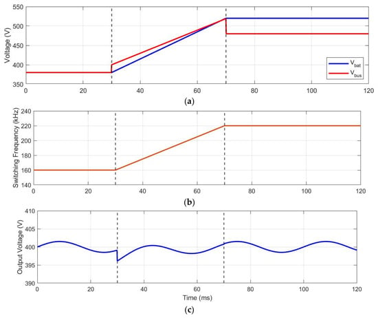
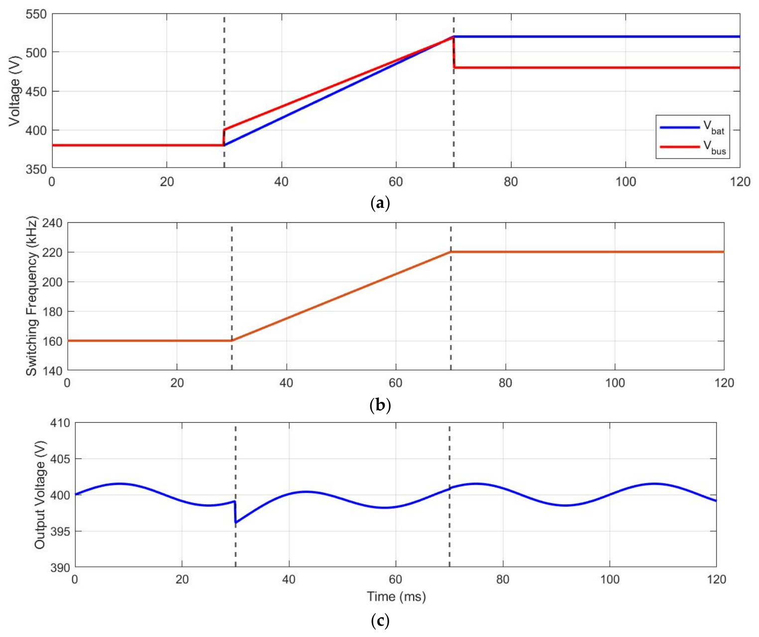
The mode transition between low-voltage mode and high-voltage mode was also tested. Figure 13 illustrates the system behavior when the battery voltage increases from 380 V to 520 V. Subplot (Figure 13a) shows the battery voltage and the corresponding adjustment of the DC-bus voltage. Subplot (Figure 13b) shows the increase in the CLLC switching frequency as the converter moves from the high-gain region to the near-resonant region. Subplot (Figure 13c) confirms that the output voltage remains well regulated with only minimal deviation during the transition. No significant oscillation or instability was observed, confirming the effectiveness of the mode selection logic and the coordination between the totem-pole front-end and the CLLC stage.
Figure 13.
Mode transition from Low-Voltage Mode to High-Voltage Mode when the battery voltage increases from 380 V to 520 V, (a) battey voltage and DC-bus voltages duirng mode transition, (b) CLLC switching frequency, and (c) output voltage.
The smooth increase in the CLLC switching frequency during the transition shows that the mode selector correctly identifies the change in required voltage gain and gradually moves the operating point from the high-gain region toward resonance. The absence of large oscillations in both the DC-bus and output voltages confirms that the bandwidths of the outer voltage loops and the frequency modulation loop are properly coordinated. This seamless behavior is essential for real EV charging profiles, where battery voltage rises continuously during the constant-current phase.
The fast recovery of the output voltage (within 7 ms) and the absence of significant overshoot demonstrate that the dual-loop control of the totem-pole stage and the frequency modulation of the CLLC stage are well coordinated. The input currents remain sinusoidal during the transient because the current loop bandwidth is sufficiently high to reject the disturbance caused by the sudden power change.
3.5. Input Current Quality and Power Factor
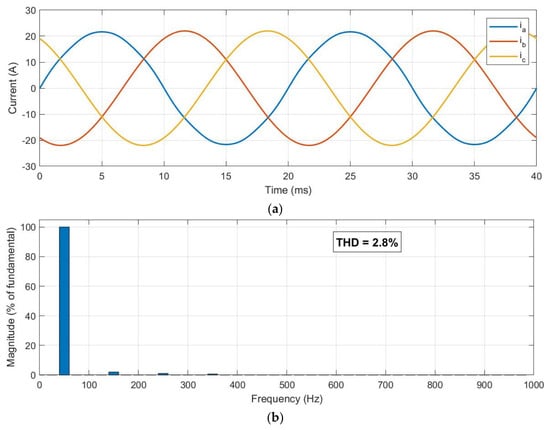
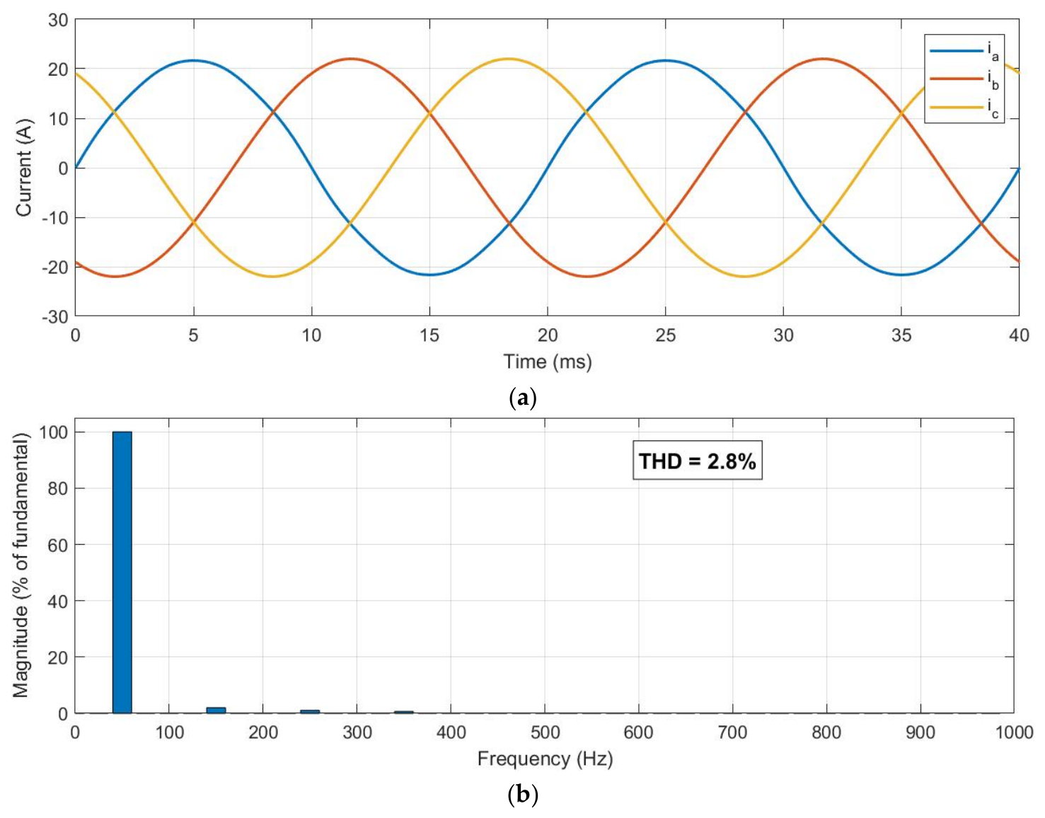
The input current quality is a critical performance metric for grid-connected EV chargers. Figure 14 shows the input current waveforms and their corresponding harmonic spectrum when the converter operates at rated power with a battery voltage of 400 V. Subplot (Figure 14a) presents the three-phase input currents, which are nearly sinusoidal and well balanced. Subplot (Figure 14b) shows the harmonic spectrum of the phase-a current. The simulated phase-a current THD is 2.8% at rated power and 400 V battery voltage (Figure 14). This is below the 5% TDD limit of IEEE 519 for . For a 22 kW three-phase rating the closer emission standard would be IEC 61000-3-12 rather than IEC 61000-3-2, which applies only to equipment rated ≤16 A per phase.
Figure 14.
Input current quality at rated power (400 V). (a) Three-phase input current waveforms. (b) Harmonic spectrum of phase-a current (THD = 2.8%).
The low harmonic content is achieved by the combination of three-phase interleaving, which cancels the major switching harmonics, and the closed-loop current control that continuously shapes the inductor currents. Even though the DC-bus voltage contains a visible low-frequency ripple due to the small film capacitors, the current controller successfully compensates for this disturbance, keeping the simulated phase—a THD at 2.8% at this operating point.
The power factor remains above 0.995 across the entire load range from 20% to 100%. Even at light load, where many conventional chargers suffer from significant current distortion, the proposed converter maintains a power factor above 0.99. This performance is achieved through the combination of the interleaved totem-pole topology and the effective current control loop, which actively shapes the input currents despite the presence of DC-bus voltage ripple caused by the small film capacitors.
3.6. Performance Comparison with Existing Solutions
To further highlight the advantages of the proposed converter, a performance comparison with several recently reported bidirectional EV chargers is presented in Table 4. The comparison considers key parameters such as topology type, rated power, output voltage range, peak efficiency, input current THD, and the use of electrolytic capacitors. Table 4 presents a performance comparison between the proposed converter and several recently reported EV charging solutions. The proposed design covers 100–850 V and uses only a 50 µF film bus. The 97.1% figure is a simulation loss-model value and is not compared as equal to the measured efficiencies in the experimental rows.
Table 4.
Performance comparison of the proposed converter with recently reported EV charging solutions.
The proposed single-stage asymmetric CLLC converter achieves a competitive peak efficiency of 97.1% while supporting one of the widest output voltage ranges (100–850 V) among the compared solutions. Unlike most two-stage chargers, the proposed design eliminates large electrolytic capacitors, which is expected to improve reliability by removing a lifetime-limiting component. Although the control complexity is slightly higher than conventional two-stage solutions, the overall system performance in terms of efficiency, voltage range, and input current quality is superior.
Compared with previously reported single-stage CLLC chargers, the proposed design demonstrates significantly better voltage regulation capability due to the asymmetric resonant tank and the optimized parameters obtained from PSO. Compared with recent accurate modeling studies of asymmetrical CLLC converters and with electrolytic-capacitor-less single-stage OBCs, the proposed design is distinguished by the simultaneous achievement of an ultra-wide output voltage range, three-phase interleaving, and the complete elimination of large electrolytic capacitors under a unified control framework [11]. This allows the converter to maintain high efficiency and wide ZVS range even at extreme battery voltages, which is a major limitation in many existing single-stage topologies [7,8,12].
3.7. Dynamic Performance and Transient Response
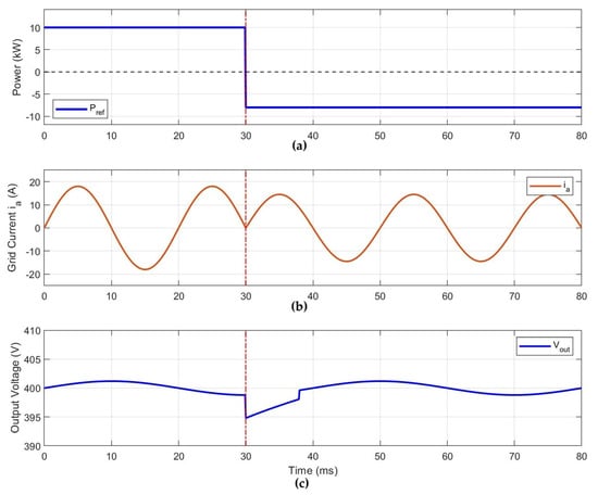
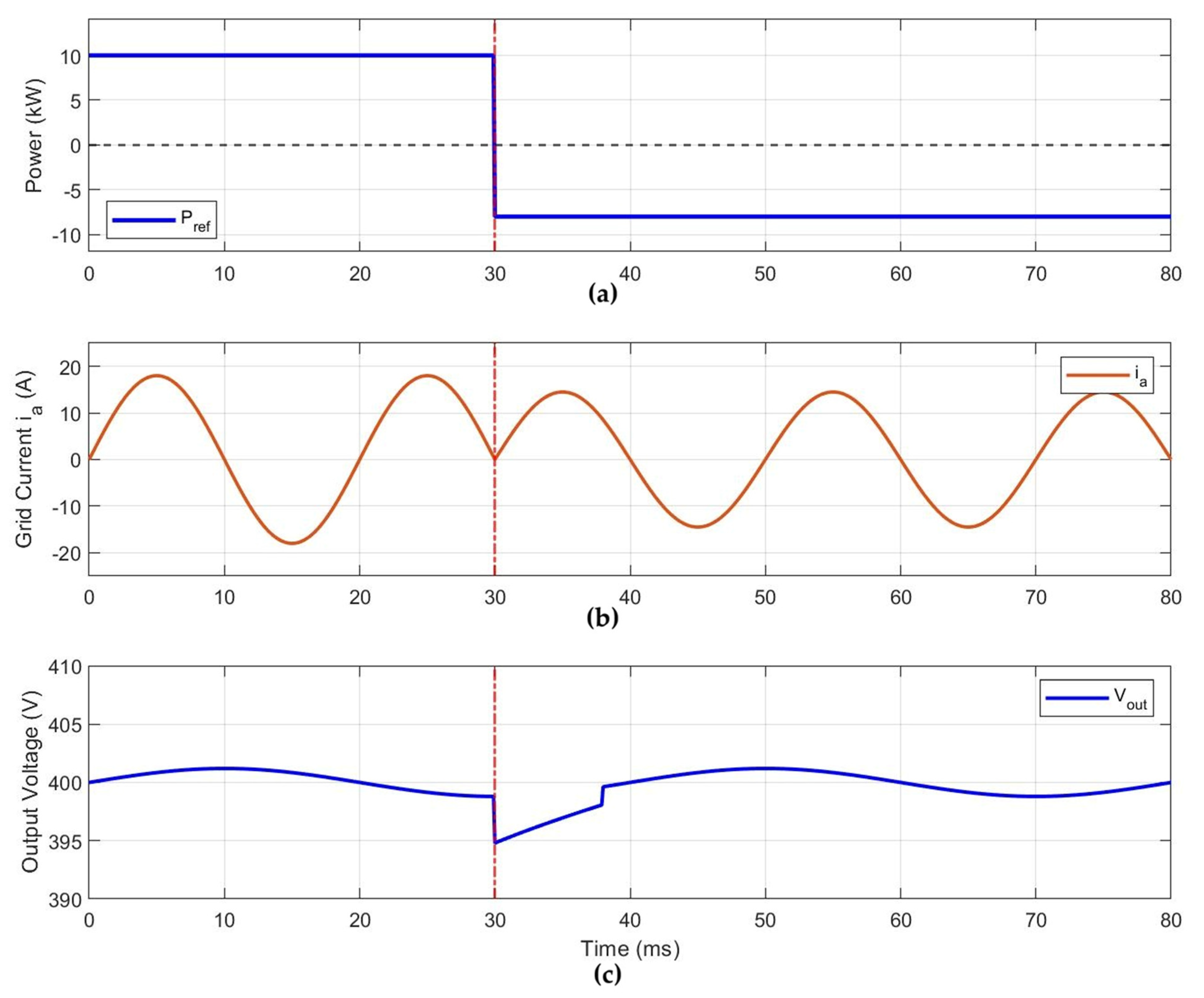
In addition to the load step and mode transition tests presented in Section 3.4, the bidirectional capability of the proposed converter was verified through a power reversal test. Figure 15 shows the system response when the power reference changes from +10 kW (G2V) to −8 kW (V2G).
Figure 15.
V2G power reversal from +10 kW (G2V) to −8 kW (V2G). (a) Power reference; (b) phase—a grid current; (c) output voltage.
Subplot (Figure 15a) illustrates the power reference step. Subplot (Figure 15b) shows that the phase—a grid current smoothly reverses direction within one grid cycle while remaining sinusoidal. Subplot (Figure 15c) confirms that the output voltage stays well-regulated with only a minor temporary deviation during the transition.
These results demonstrate that the proposed control strategy supports seamless bidirectional power flow and maintains stable operation during V2G mode, which is essential for vehicle-to-grid applications.
4. Discussion and Conclusions
This paper has presented the design and multi-objective optimization of a single-stage bidirectional AC-DC converter that integrates a three-phase interleaved totem-pole front-end with an asymmetric CLLC resonant converter for wide-voltage-range EV charging applications. The proposed topology eliminates the need for large electrolytic DC-bus capacitors by using only small film capacitors, while enabling seamless operation across an ultra-wide battery voltage range of 100–850 V.
The asymmetric CLLC resonant tank was systematically designed using fundamental harmonic approximation (FHA), time-domain analysis (TDA), and multi-objective particle swarm optimization (PSO). The optimized parameters provide a high voltage gain capability and maintain zero-voltage switching (ZVS) down to approximately 18% load on the primary side and 15–25% load on the secondary side across the full voltage range. Simulation results confirm a peak efficiency of 97.1% at the nominal operating point (400 V) and efficiency above 95% even at light load. The loss analysis shows that the dominant losses are conduction losses in the totem-pole switches and the resonant inductors, while switching losses remain low due to the wide ZVS range.
The converter also demonstrates good input current quality, with a simulated THD of 2.8% at rated 400 V operation and a power factor above 0.995 from 20% to 100% load. Dynamic tests verify fast recovery during load steps, smooth transition between low-voltage and high-voltage modes, and reliable bidirectional power flow (V2G). The performance comparison with recently reported solutions highlights that the proposed design achieves one of the widest output voltage ranges while eliminating electrolytic capacitors and maintaining competitive efficiency.
Despite these advantages, the control system is more complex than that of conventional two-stage chargers due to the need for coordinated mode selection, frequency modulation, and adaptive dead-time control [9,11]. In addition, efficiency at the extreme ends of the voltage range is slightly lower than at nominal conditions. These trade-offs are typical of wide-range single-stage designs and remain topics for further improvement [10].
Several limitations should be stated. First, all results come from time-domain simulation and have not been checked on hardware. PCB trace inductance, extra transformer leakage, and gate-driver loop inductance are not modeled as separate elements; Figure 11 shows that a ± 10% change in still keeps primary ZVS between 16.7% and 19.5% load. Second, the unified control is more complex than a conventional two-stage onboard charger. Third, efficiency is slightly lower near 100 V and 850 V than at 400 V. Finally, thermal behavior and EMI are not analyzed. No EMI filter or conducted/radiated spectrum is given for the 150–250 kHz GaN/SiC edges, and no thermal map of the 50 µF film bus is given. The electrical stress used for that bank is the 28 V peak-to-peak ripple and the 1.1 A low-frequency RMS current in Figure 9. Future work will address experimental validation, thermal and EMI characterization, and cost-aware control.
In conclusion, the combination of an interleaved totem-pole front-end with an optimized asymmetric CLLC resonant stage offers a high-efficiency, electrolytic-capacitor-free solution for next-generation 800 V-class EV onboard chargers requiring 100–850 V operation and bidirectional capability.
Author Contributions
Conceptualization, G.P. and L.P.; methodology, G.P., A.L. and L.P.; software, A.L.; validation, A.L.; formal analysis, A.L. and L.P.; investigation, L.P.; resources, G.P. and L.P.; data curation, A.L. and L.P.; writing—original draft preparation, A.L. and L.P.; writing—review and editing, G.P. and A.L.; project administration, G.P.; funding acquisition, L.P. All authors have read and agreed to the published version of the manuscript.
Funding
This research was supported by Zhejiang Provincial Public Welfare Technology Application Projects of China under Grant No. LGG22E090003; Key R&D Program of Hangzhou City, China (2025SZD2A09).
Data Availability Statement
The original contributions present in the study are include in the article. Further inquiries can be directed to the corresponding authors.
Conflicts of Interest
The authors declare no conflicts of interest.
Abbreviations
The following abbreviations are used in this manuscript:
| CCM | Continuous conduction mode |
| DSP | Digital signal processor |
| EMI | Electromagnetic interference |
| ESR | Equivalent series resistance |
| FHA | Fundamental harmonic approximation |
| GaN | Gallium nitride |
| ICE | International Electrotechnical Commission |
| IEEE | Institute of Electrical and Electronic Engineers |
| PF | Power factor |
| PFM | Pulse-frequency modulation |
| PSO | Particle swarm optimization |
| RMS | Route mean square |
| SiC | Silicon carbide |
| SPWM | Sinusoidal pulse-width modulation |
| TCM | Triangular conduction mode |
| TDD | Total demand distortion |
| THD | Total harmonic distortion |
| ZCD | Zero-current detection |
| ZVS | Zero-voltage switching |
References
- Zhu, H.; Hu, S.; Fujishima, N.; Onishi, Y. Design Method of Totem-Pole PFC and CLLC Resonant Converter Based on SiC MOSFET. In Proceedings of the 2021 6th International Conference on Power and Renewable Energy, ICPRE 2021, Shanghai, China, 17–20 September 2021; pp. 383–389. [Google Scholar] [CrossRef] [Scilit]
- Mishra, D.P.; Deshmukh, A.D.; Kalyan, M.P.; Ray, I.; Lenka, R.K. Efficient On-Board EV Battery Charger Using LLC Resonant Converter and Totem-Pole PFC. In Proceedings of the 3rd International Conference on Power Electronics and Energy, ICPEE 2025, Bhubaneswar, India, 14–16 December 2025. [Google Scholar] [CrossRef] [Scilit]
- Kushwaha, S.; Parakh, A. Design & Simulation of Totem-Pole PFC integrated LLC Resonant Converter for EV Application. In Proceedings of the 2025 IEEE International Conference on Interdisciplinary Approaches in Technology and Management for Social Innovation, IATMSI 2025, Gwalior, India, 6–8 March 2025. [Google Scholar] [CrossRef] [Scilit]
- Fu, Q.; Wang, Y.; Wang, B.; Zeng, Y.; Zhou, X.; Lu, Z. A single-stage AC/DC electric vehicle charging converter with an integrated CLLC resonant circuit. Sustain. Energy Technol. Assess. 2026, 85, 104825. [Google Scholar] [CrossRef] [Scilit]
- Yuan, J.; Poorfakhraei, A.; Emadi, A. A Novel Phase Shift Control for Single-Stage Bidirectional Isolated Totem-Pole AC/DC Onboard Electric Vehicle Chargers. In Proceedings of the 2023 IEEE Transportation Electrification Conference and Expo, ITEC 2023, Detroit, MI, USA, 21–23 June 2023. [Google Scholar] [CrossRef] [Scilit]
- Hamdi, R.; Torkaman, H.; Amraei, A. Enhanced On-Board Charger Performance Using Model Predictive Control with Interleaved Totem Pole PFC Based on Asymmetrical CLLC Converters. In Proceedings of the 2024 4th International Conference on Electrical Machines and Drives, ICEMD 2024, Tehran, Iran, 24–25 December 2024. [Google Scholar] [CrossRef] [Scilit]
- Wang, Y.; Wang, F.; Zhuo, F.; Yu, K.; Tian, J.; Zhang, X. Synchronous Rectification and Parameter Design Based on Accurate Time-Domain Model for Asymmetrical CLLC Resonant Converter. IEEE Trans. Transp. Electrif. 2025, 11, 4681–4697. [Google Scholar] [CrossRef] [Scilit]
- Li, B.; Chen, M.; Sun, X.; Wang, J.; Jiang, F. A Hybrid Control for Smooth Power Direction Transition of Bidirectional Resonant CLLC Converter with Wide Voltage Gain. IEEE Trans. Power Electron. 2024, 39, 15898–15914. [Google Scholar] [CrossRef] [Scilit]
- Zhou, B.; Zhao, C.; Luo, H.; Qiu, Y.; Chen, S.; Zang, T.; Zhou, Y.; Zhou, X.; Zhao, H. Hybrid Control Strategy for Single-Stage Interleaved Totem-Pole LLC AC-DC Converter with Input and Output Power Decoupling. IEEE Trans. Power Electron. 2024, 39, 5135–5154. [Google Scholar] [CrossRef] [Scilit]
- Gurara, F.; Etta, D.; Afridi, K.K. Wide Operating Range Single-Stage Bidirectional Impedance Control Network-based Onboard Electric Vehicle Charger. In Proceedings of the IEEE Applied Power Electronics Conference and Exposition—APEC, Long Beach, CA, USA, 25–29 February 2024; pp. 1694–1699. [Google Scholar] [CrossRef] [Scilit]
- Kim, H.; Park, J.; Lee, J.; Choi, S. A Simple Modulation Strategy for Full ZVS of Single-Stage Electrolytic Capacitor-Less EV Charger with Universal Input. IEEE Trans. Power Electron. 2022, 37, 12030–12040. [Google Scholar] [CrossRef] [Scilit]
- Derakhshan, S.; Lam, J. A Half-Bridge/Dual Stacked-Switches Structured AC/DC Electrolytic Capacitor-Less Bidirectional Converter with Soft-Switching for High-Voltage EV Charger. IEEE Trans. Power Electron. 2025, 40, 10912–10930. [Google Scholar] [CrossRef] [Scilit]
- Paul, S.; Singh, A.; Bhuse, T.; Martin, T.; Nguyen, H.; Vedula, I.; Milivojevic, N.; Maksimović, D.; Corradini, L. A Universal DC Fast Charging Front-End with Optimized Film Capacitor Design. In Proceedings of the IEEE Applied Power Electronics Conference and Exposition—APEC, Atlanta, GA, USA, 16–20 March 2025; pp. 54–61. [Google Scholar] [CrossRef] [Scilit]
- Dizji, R.H.; Zolghadri, M.R. A New Approach Of DC-Link Capacitor Design For 6.6kw E-Cap less Single-Phase On-Board EV charger. In Proceedings of the 2025 16th Power Electronics, Drive Systems, and Technologies Conference, PEDSTC 2025, Tehran, Iran, 4–6 February 2025. [Google Scholar] [CrossRef] [Scilit]

Disclaimer/Publisher’s Note: The statements, opinions and data contained in all publications are solely those of the individual author(s) and contributor(s) and not of MDPI and/or the editor(s). MDPI and/or the editor(s) disclaim responsibility for any injury to people or property resulting from any ideas, methods, instructions or products referred to in the content. |
© 2026 by the authors. Licensee MDPI, Basel, Switzerland. This article is an open access article distributed under the terms and conditions of the Creative Commons Attribution (CC BY) license.