


Abstract
Current source inverters (CSIs) have exhibited significant potential in variable-speed motor drive applications, attributed to their superior dynamic response and robust anti-interference capabilities. Space vector pulse-width modulation (SVPWM) is renowned for its exceptional performance and has been extensively adopted in CSIs. Nevertheless, the implementation of SVPWM is substantially more complex than that of carrier-based pulse-width modulation (CBPWM). This paper proposes a CBPWM strategy for CSIs that achieves full equivalence to SVPWM while delivering enhanced implementation simplicity, computational efficiency, and reduced processor resource demand. In that approach, three-phase pseudo-modulated signals are compared with a triangular carrier waveform to generate three two-level PWM signals. Subsequently, pairwise subtraction of these two-level signals yields three three-level PWM signals. In addition, the injection of zero-sequence current enables the same DC current utilization rate as that achieved by SVPWM. The devices within each bridge arm are then controlled according to the three-level PWM signals, enabling the output of desired current pulses for the CSI. The proposed CBPWM scheme determines all switching states, duty cycles, and switching sequences through straightforward carrier comparisons and basic arithmetic operations, thereby eliminating the need for computationally intensive sinusoidal calculations while achieving equivalence to the SVPWM method. Simulation and experimental results demonstrate that the output performance of CBPWM is equivalent to that of SVPWM, while also validating the proposed method’s structural simplicity and computational efficiency for CSIs.
1. Introduction
Based on the difference in DC sources, inverters are categorized into voltage source inverters (VSIs) and current source inverters (CSIs). Two-level VSIs are characterized by their simple structure and ease of control, which have led to their widespread adoption in DC–AC power conversion applications [1]. Although CSIs are currently not as prevalent as VSIs, they offer motor-friendly output waveforms, superior boost capability, and inherent short-circuit protection [2,3]. Owing to these advantages, CSIs are anticipated to find application in electric vehicles, offshore wind farms, and other domains. For motors, the utilization of CSIs-based drives represents a future trend [4,5].
Pulse-width modulation (PWM) serves as the core control technique in power electronic converters, playing a pivotal role in determining the quality of output voltage and current. For inverters, PWM synthesizes target waveforms through high-frequency switching actions; so, the optimization of PWM is essential for enhancing performance metrics such as harmonic suppression, switching loss reduction, and efficient dc-link utilization. Carrier-based PWM (CBPWM) was initially applied to VSIs [6,7], and the earliest form of PWM modulation utilized sinusoidal wave signals. By incorporating a zero-sequence signal [8], the modulation signal can be transformed into a non-sinusoidal waveform, thereby extending its linear modulation range without affecting line-to-line current and voltage characteristics. With the development of microprocessor, space-vector pulse-width modulation (SVPWM) was developed and quickly became the predominant modulation method [9,10,11,12]. That technique is extensively utilized in both VSIs and CSIs [13,14], recognized for its well-defined physical significance and superior harmonic performance. However, SVPWM entails computationally demanding operations including space-vector localization and trigonometric computations that impose substantial processing requirements on digital control hardware. Critically, with the increase in switching frequency, the permissible computation time per PWM cycle diminishes progressively, thereby compromising the real-time feasibility of SVPWM implementation [15,16,17].
Extensive research has been conducted on various space vector modulation strategies for CSIs, leading to their promising application prospects across multiple domains. In doubly-fed induction generator systems, the integration of CSIs offers enhanced system robustness, inherent short-circuit protection, and superior fault ride-through capability [18]. In photovoltaic power generation systems, CSIs are employed as grid-connected inverters, and corresponding control strategies have been developed to ensure system stability and mitigate common-mode leakage current [19,20]. In motor drive applications, CSI-fed motors exhibit improved dynamic and steady-state performance, while the adoption of silicon carbide power devices enables higher switching frequencies [21,22]. Moreover, CSI topologies have evolved toward greater complexity, including back-to-back configurations [23], multilevel architectures [24], and multiphase machine interfaces [25]. To date, current vector synthesis-based modulation remains the predominant control paradigm in practical CSI implementations across these application areas. Nevertheless, SVPWM necessitates real-time computation of vector durations and sequences, resulting in significant computational complexity. In contrast, CBPWM is simple and easy to implement, requiring fewer computing resources.
The equivalent relationship between CBPWM and SVPWM in VSIs has already been demonstrated [26,27]. These modulation techniques generate identical switching patterns with equivalent duty cycles when properly implemented [28]. Notably, CBPWM can achieve complete functional parity with SVPWM by incorporating appropriate zero-sequence components into modulation signals, thereby replicating identical voltage vector trajectories and switching sequences while preserving equivalent DC voltage utilization and harmonic characteristics [29,30,31]. For VSIs, the switching logic is controlled by two-level signals for each phase, that is, the upper bridge arm is on and the bottom bridge arm of the same phase off, or the two are switched. There is no situation where the upper and bottom arms are turned on or turned off simultaneously. But in CSIs, such a situation does exist. Therefore, CSIs require a three-level logic signals for control each phase, which is quite different from VSIs. Additionally, SVPWM remains the dominant modulation approach for CSIs, while CBPWM remains relatively underexplored [32]. The fundamental duality principle governing VSI and CSI operation strongly suggests that CBPWM should be equally applicable to CSIs, offering potential implementation simplifications. That theoretical symmetry motivates the development of computationally efficient CBPWM algorithms for CSIs, which could significantly reduce controller resource requirements while maintaining performance parity with SVPWM [33].
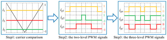
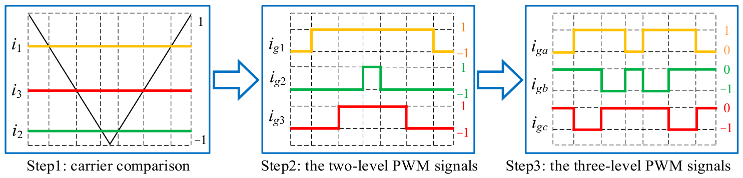
This paper introduced a fast carrier-based modulation for CSIs. The proposed scheme demonstrates significant computational advantages over conventional SVPWM for CSIs. The implementation involves three key steps: (1) generating two-level PWM signals through comparison between three-phase references and a triangular carrier wave, (2) deriving three-level PWM signals through pairwise subtraction of those two-level signals, and (3) applying the resulting three-level PWM to control the CSI. Furthermore, the study establishes comprehensive theoretical relationships between SVPWM and the proposed CBPWM method for CSIs, demonstrating that both methods produce switching states with identical duty cycles, thereby proving their functional equivalence. Moreover, within each PWM cycle, the CBPWM strategy exhibits significantly lower computational complexity and implementation overhead compared to SVPWM, resulting in reduced instruction-cycle consumption and more efficient utilization of embedded processing resources.
The rest of this paper is organized as follows. Section 2 presents the working principles of CSIs and provides the theoretical foundation for space-vector modulation in CSI applications. Section 3 details the proposed fast CBPWM implementation specifically designed for CSIs. Section 4 conducts a comprehensive analysis of the mathematical relationships between SVPWM and CBPWM techniques in CSI systems. To validate the functional equivalence between the proposed CBPWM method and conventional SVPWM, extensive verification was performed through both simulation studies and experimental prototypes. The simulation results are presented in Section 5, followed by experimental verification in Section 6. Finally, Section 7 concludes the paper with key findings and contributions.
2. Current Space-Vector PWM for CSIs
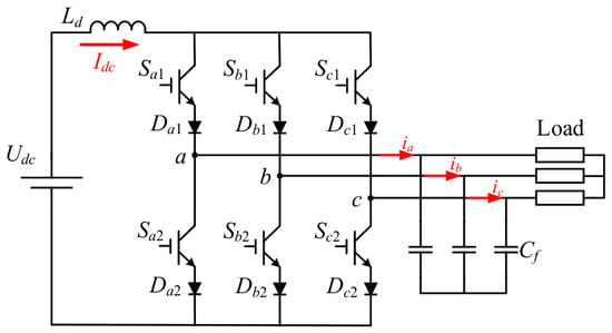
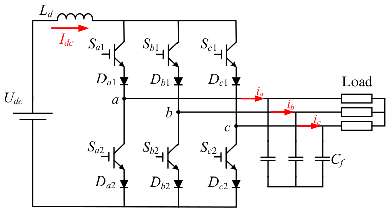
Figure 1 illustrates the topology of a three-phase current source inverter, which consists of six bridge legs comprising series-connected fully controlled a power device and a power diode. The large inductor Ld on the DC side is connected in series with the DC voltage source Udc, ensuring the provision of a steady current Idc. The capacitor on the AC side serves to filter out high-frequency current components, thereby enabling the fundamental sinusoidal current to flow into the three-phase load, such as a motor.
Figure 1.
The circuit of a current source inverter.
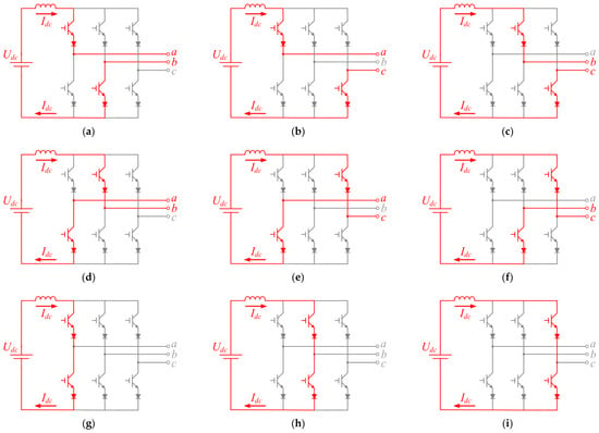
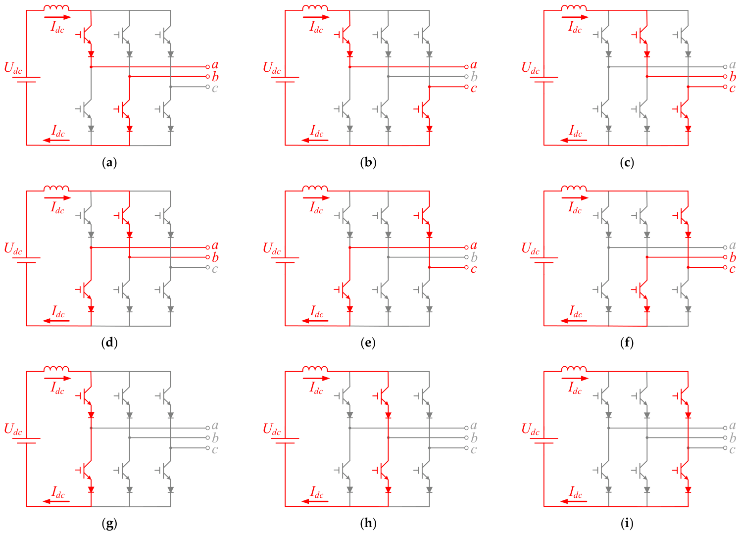
At any moment, it is necessary to ensure that at least one upper switch and one bottom switch are turned on to maintain continuous current flow for CSIs. Usually, only one upper switch and one bottom switch are designed to be conductive to improve the waveform quality of the output. Therefore, there are 9 switching combinations for current source inverters, as shown in Figure 2 and Table 1. The six active switching states are (Sa1, Sb2), (Sa1, Sc2), (Sb1, Sc2), (Sb1, Sa2), (Sc1, Sa2), and (Sc1, Sb2), each enabling distinct phase current paths. And three zero states are (Sa1, Sa2), (Sb1, Sb2), and (Sc1, Sc2); each may be used to regulate current by diverting it through the same phase bridge legs. By sequencing these states, the inverter synthesizes controlled, three-phase AC voltage waveforms from the DC current input.
Figure 2.
The current path for each switching state. (a) Switching state (Sa1, Sb2). (b) Switching state (Sa1, Sc2). (c) Switching state (Sb1, Sc2). (d) Switching state (Sb1, Sa2). (e) Switching state (Sc1, Sa2). (f) Switching state (Sc1, Sb2). (g) Switching state (Sa1, Sa2). (h) Switching state (Sb1, Sb2). (i) Switching state (Sc1, Sc2).
Table 1.
Switching combinations for CSIs.
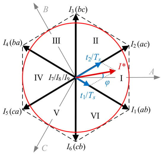
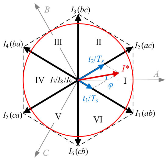
Currently, the SVPWM method is employed to generate PWM signals for CSIs in practical applications. Figure 3 illustrates the map of current space-vectors for CSIs. If ia, ib, and ic are three-phase symmetrical sinusoidal currents with an angular frequency of ω, then the magnitude of the synthesized vector I* defined by Equation (1) is equal to the peak value of the alternating phase current, and it is a current vector rotating at a uniform angular velocity of ω. Then the projections of the rotating vector I* on the A, B, and C axes are the instantaneous values of the three-phase currents ia, ib, and ic.
Figure 3.
Current space vectors map of CSIs.
According to the definition in Equation (1), the spatial distribution of current vectors for the 9 switch combinations are shown in Figure 3, among which the magnitude of the active vectors is equal to 4Idc/3. There are six active vectors I1, I2, …, I6, whose phases differ by 60° from each other in space, and three zero vectors I7, I8, I9, which do not generate output current and can be used to make up for the remaining time during which the active vectors are not acting.
Let t1, t2, …, t9 denote the dwell times corresponding to space vectors I1, I2, …, I9, respectively.
where Ts is the sampling time.
In one sampling interval, the output current vector is
where I* is the reference current vector.
To reduce the number of switching actions and harmonics, the reference vector I* can be decomposed into two nearest adjacent vectors, as illustrated in Figure 3. Since the zero vectors I7, I8, and I9 have no contributions to the reference current vector I*, the three vectors are equivalent in terms of the output of the current. In order to minimize the switching frequency, different sectors use their own specially selected zero vector. In Sector I and Sector IV, the adopted zero vector is I7; in Sector II and Sector V, zero vector is I9; in Sector III and Sector VI, zero vector is I8. For instance, in Sector I, the current vector can be decomposed accordingly.
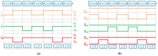
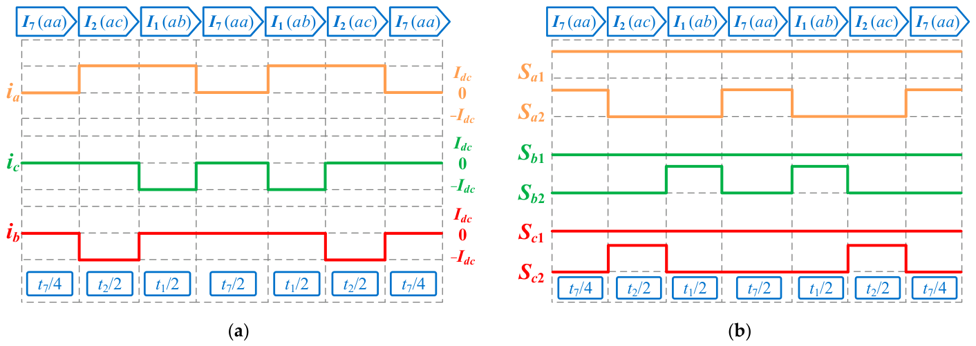
In Sector I, the zero vector I7 is selected to occupy the residual time interval. Following the center-symmetric seven-segment sequence employed by VSIs, Figure 4a illustrates the switching sequences for the current vectors of CSIs. Figure 4b further depicts the drive signals for the six switching devices. Within this sector, the upper switching device of phase-a maintains continuously conducting, while the three bottom devices are switched alternately to ensure a conducted path for the DC current. Switching sequences for the current vectors in the remaining five sectors can be derived following the methodology presented in Figure 4.
Figure 4.
The switching sequences of the current space vector in sector I. (a) The timing diagram for vectors I1, I2, and I7. (b) The timing diagram of gate drive signals.
Let the length of the current vector I* be μIdc. According to the equal ampere-second principle, the two blue vectors and the red vector within Sector I in Figure 3 can be connected to form a closed triangle, the Law of Sines can be applied for the triangle to derive the following relationship:
where φ represents the angle at which the synthesized vector I* spreads counterclockwise along the A-axis.
According to Equation (5), the dwell times of t1 and t2, as well as the dwell time t7 for the zero vector I7 can be expressed as:
Based on the modulation solution established for the sector I, Table 2 summarizes the switching vectors and dwell times for the remaining five sectors. For SVPWM, the synthesized current vector maintains a constant magnitude, tracing a circular trajectory as the red circle in Figure 3. The maximum achievable AC output current occurs when this circular path aligns with the hexagon’s inscribed circle, expressed by μIdc=.
Table 2.
The dwell time of current vectors for the six sectors.
3. The Proposed CBPWM Scheme for CSIs
The three-phase current references generated by the controller are , , and :
where θ is the phase angle of the three-phase symmetrical references, and m is the modulation index, defined as the ratio of the peak value of the output fundamental current to the DC current.
Then, the references , , and are linearly converted to the three-phase pseudo-modulation signals , , and :
Introducing the zero-sequence signal iz(t) as follow:
where k is zero-sequence signal distribution factor, and function min{·} and max{·} represent the minimum and maximum value, respectively. For linear modulation, the maximum value of the modulation index m can reach 1.
To enhance the modulation index, the zero-sequence single can be injected into the pseudo-modulation signals as follows:
After obtaining the pseudo-signals with injected zero-sequence signal, the carrier comparison can be performed. As shown in Figure 5, the pseudo-modulation signals ix(t) are compared with a symmetrical triangular carrier signal ic(t), generating the two-level PWM signals igx(t) between 1 and −1.
Figure 5.
The flowchart of carrier-based PWM scheme for CSIs.
Three-level PWM signals for CSIs, which take values of 1, 0, and −1, are subsequently generated by performing pairwise subtraction of the two-level phase-leg PWM signals.
The switching logic operates such that a PWM signal value of 1 activates the corresponding upper bridge leg, while a value of −1 activates the corresponding bottom bridge leg. Simultaneously, precisely one upper bridge leg and one bottom bridge leg are conducting, necessarily in different phases when none of the three PWM signals is zero. This switching scheme ensures that, for the three-phase PWM signals, at most one signal transitions holds the high and low states concurrently. During intervals where all three-phase PWM signals simultaneously equal 0, the upper and bottom switches within the same phase conduct simultaneously to provide a continuous path for the DC current. Consequently, the three-phase AC output currents are zero. When the three-phase PWM signals are all zero, the shoot-through state is applied to the bridge leg corresponding to the phase current exhibiting opposite polarity to the other two phases.
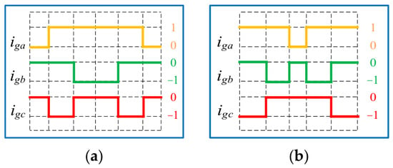
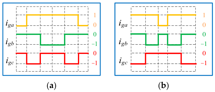
PWM schemes can be divided into continuous PWM and discontinuous PWM (DPWM) by terms of the switching characteristics. When the zero-sequence signal subjects to −1 − imin < iz(t) < 1 − imax, PWM schemes are continuous PWM. During each carrier cycle, all two-level PWM signal change between −1 and +1 twice; so, the three-level PWM signal changes 4 times, and the corresponding inverter bridge leg is also switched on or off 4 times. When the zero-sequence signal satisfies iz(t) = −1 − imin or iz(t) = 1 − imax, PWM schemes are DPWM, which are shown in Figure 6. Obviously, in each carrier cycle, one pseudo-modulation signal will be clamped to “1” or “−1”, and the number of switching action is reduced to 2; it is clearly that the number of switching actions of the two legs will be also changed to 2 times. Thus, the average switching frequency can be reduced by 33%.
Figure 6.
The sequences of DPWM signals for CSIs. (a) DPWM with k = 0; (b) DPWM with k = 1.
4. Relationship Between CBPWM and SVPWM
The CBPWM scheme designed for CSIs is inherently equivalent to the SVPWM method, as can be observed by comparing both Figure 4 and Figure 5. According to the equal ampere-second principle, the dwell time of the two active vectors remains constant. For SVPWM, the calculation of the dwell time is based on that principle. However, for CBPWM, the dwell time of the effective output current is determined by the difference between the two modulation signals, and the injection of the zero-sequence signal has no influence on the dwell time of the active vectors. Instead, the injection of the zero-sequence component only redistributes the dwell time of the zero vectors among the middle and side positions. The value of the three-phase modulation signal of SVPWM in Sector I calculated according to the sequence in Figure 4 are
Substitution of Equation (6) into Equation (13) yields:
By comparing Equations (7) and (14), the amplitude and phase relationship between the two modulation methods is thus expressed as:
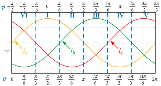
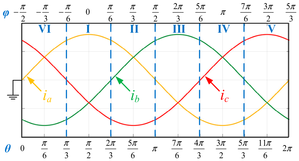
Thus, the relationship defined in Equation (15) can be extended to the remaining five sectors. Figure 7 illustrates the three-phase symmetrical current modulation signals over one fundamental period, along with the corresponding space vector sector division. Additionally, the figure shows the mapping relationship between the vector modulation angle φ and the carrier comparison angle θ across all six sectors.
Figure 7.
The mapping diagram of modulated signals.
Based on the Equal Current-Second principle for pseudo-modulation signals, in Sector I, we have
where t0 is the total dwell time of the zero vector. Within this, t01 is the dwell time of the central zero vector pulse in the seven-segment symmetric PWM sequence, and t02 is the dwell time allocated to each of the two identical zero vector pulses at the segment boundaries.
Therefore, the zero-sequence signal iz in Sector I can be expressed as Equation (17).
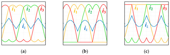
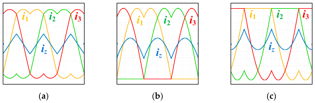
There are infinite different ways to distribute t01 and t02. Different distributions of t01 and t02 yield different space-vector modulations. Obviously, it is easy to find an equivalent distribution of zero vector for any zero-sequence signal. Figure 8 presents the time-domain waveforms of the modulation signals within one line cycle when different zero-sequence components are injected. Figure 8a shows the pseudo-modulated signal with injected zero-sequence component for k = 0.5. The carrier-based modulation of that signal produces results identical to the seven-segment symmetric-mode SVPWM implementation shown in Figure 4. Figure 8b,c illustrate two of the most common DPWMs: one clamps the three-phase pseudo-modulation signals to the minimum value in turn, that is, k = 0; and the other clamps them to the maximum value in turn, that is, k = 1. Thus, one phase always remains constant in output, which can reduce the switching actions. By establishing the relationship between the proposed CBPWM and SVPWM, and the relationship between zero-sequence signal of CBPWM and zero vector of SVPWM, it can be obtained that the two methods are equivalent.
Figure 8.
The modulation signals with injected zero-sequence. (a) (k = 0.5); (b) (k = 0); (c) (k = 1).
5. Simulation Results
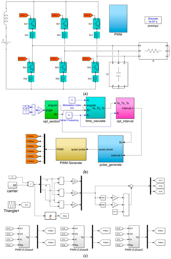
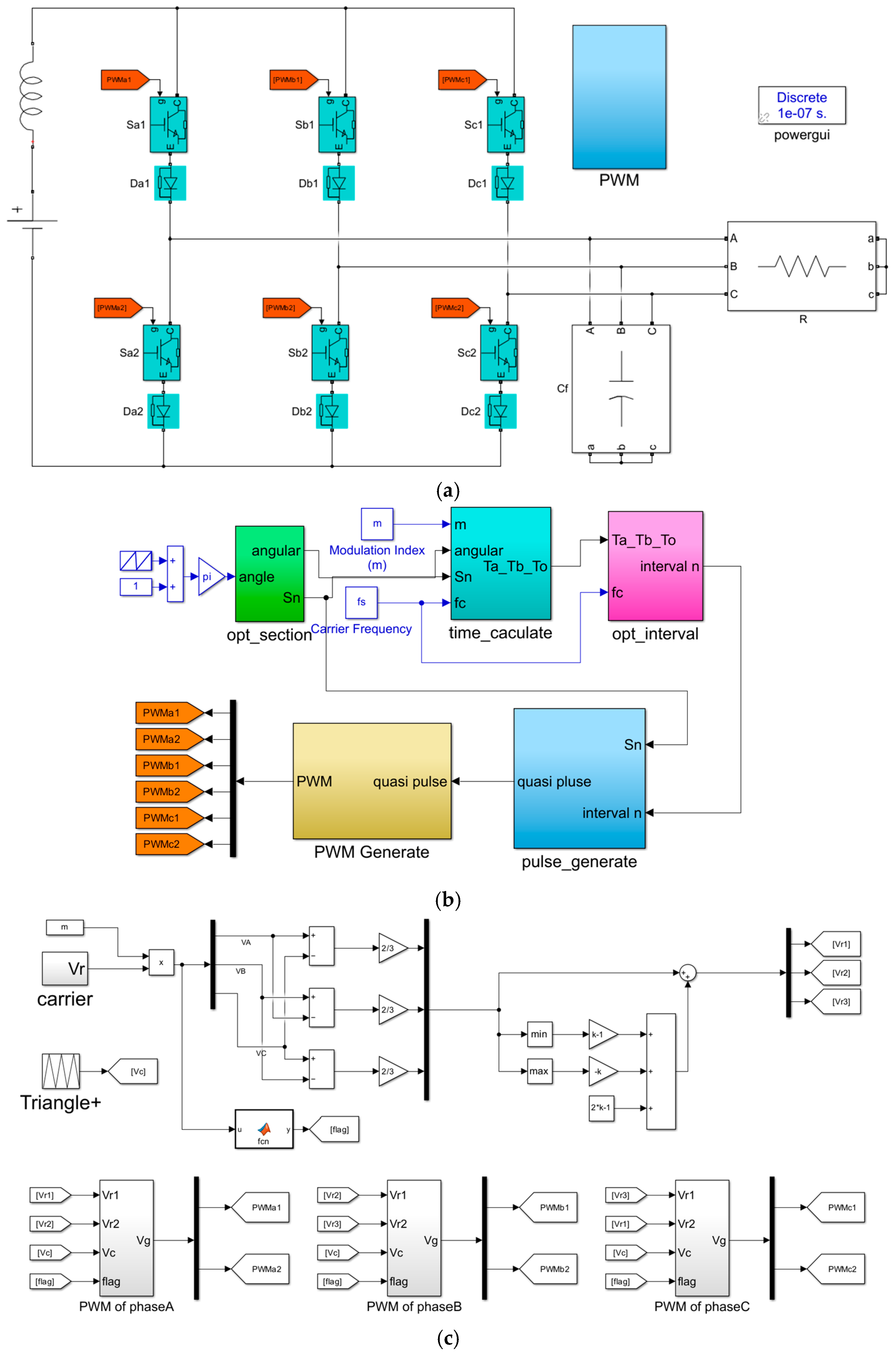
The simulations are carried out with MATLAB/Simulink R2025a, and the schematic and block diagram for the performed simulation are shown in Figure 9. Specifically, the current source consists of a voltage source in series with an inductor-like practical situation instead of an ideal current source. Figure 9a illustrates the overall schematic of the CSI, while Figure 9b,c depict the PWM implementation block diagrams for SVPWM and CBPWM, respectively.
Figure 9.
Schematic and block diagram for the performed simulation. (a) Simulation schematic for CSI. (b) Block diagram for SVPWM. (c) Block diagram for CBPWM.
The modulation index is set to 0.85, while the switching frequency is configured at 20 kHz. The current source output is maintained at 5 A, with the DC-side voltage source set to 50 V and the inductance value fixed at 0.5 mH. The filter capacitor on the AC side is 35 μF, and the load impedance is 10 Ω. All system parameters are summarized in Table 3.
Table 3.
System parameters for both simulation and experiments.
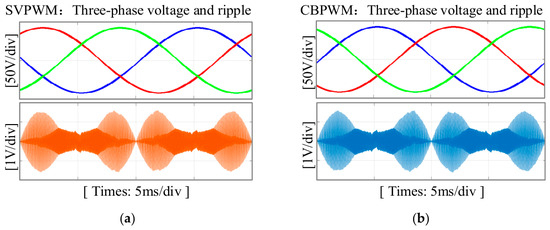
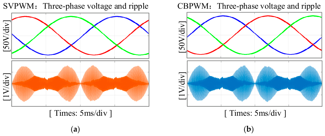
The simulation results of output voltage and voltage ripple are plotted in Figure 10. The result clearly demonstrates that, under identical conditions, the three-phase output voltages produced by both SVPWM and proposed CBPWM exhibit remarkable consistency in waveforms. Notably, the voltage amplitudes generated by both modulations maintain complete correspondence, further validating the equivalent performance.
Figure 10.
Simulation result of output voltage and ripple. (a) Space-vector PWM. (b) Carrier-based PWM.
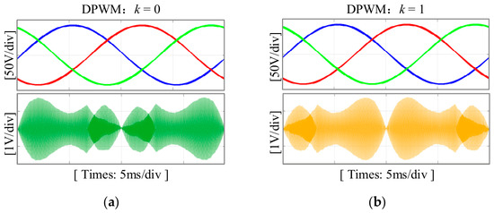
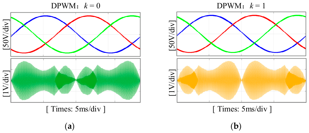
To validate the feasibility of the proposed carrier-based modulation scheme under DPWM conditions, simulations were also conducted for both k = 0 and k = 1 cases. The resulting load voltage and voltage ripple waveforms using DPWM are shown in Figure 11. These results demonstrate that the proposed carrier-based modulation scheme remains feasible for DPWM applications.
Figure 11.
Output voltage and ripple for DPWM. (a) DPWM (k = 0); (b) DPWM (k = 1).
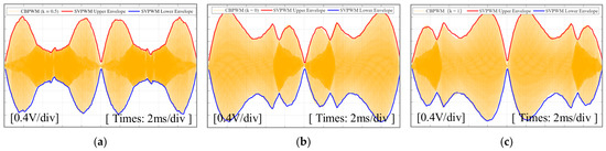
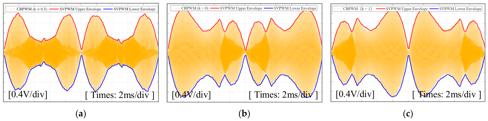
Figure 12 shows comparison of voltage ripple between CBPWM and equivalent SVPWM schemes, based on the continuous PWM and DPWM. By comparing the voltage ripples of the output voltage waveforms of the two modulation methods, it can be found that the waveforms of the two ripples overlap highly; so, the two modulation methods are equivalent.
Figure 12.
Comparison of voltage ripples between SVPWM and equivalent CBPWM schemes. (a) Continuous PWM (k = 0.5); (b) DPWM (k = 0); (c) DPWM (k = 1).
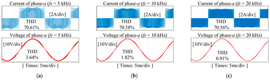
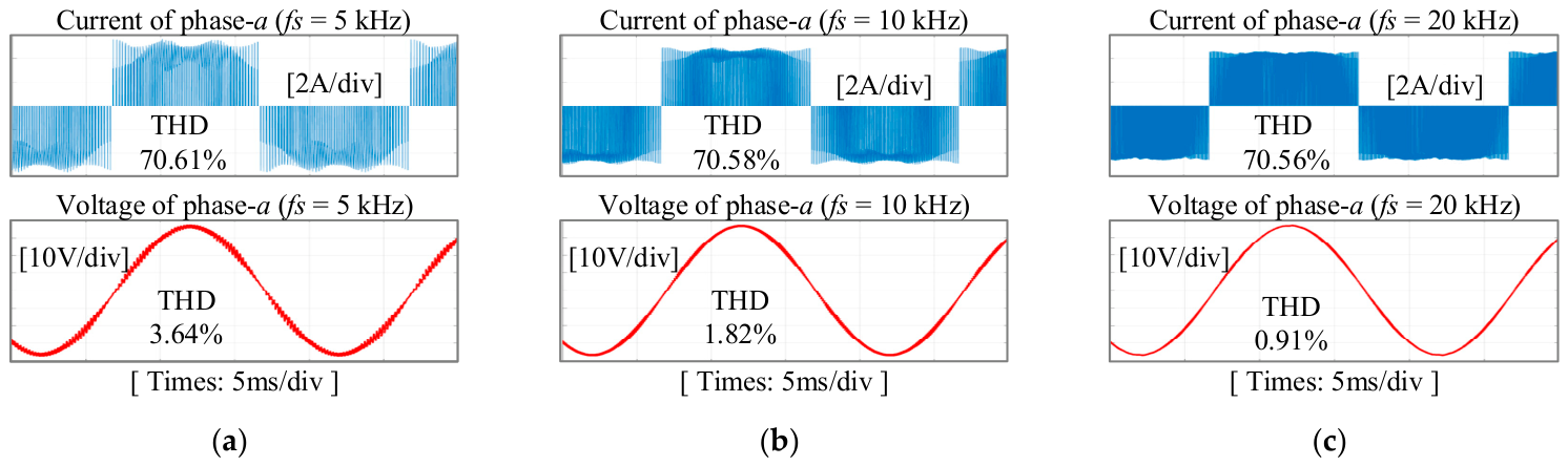
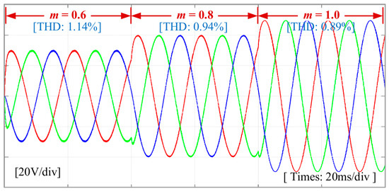
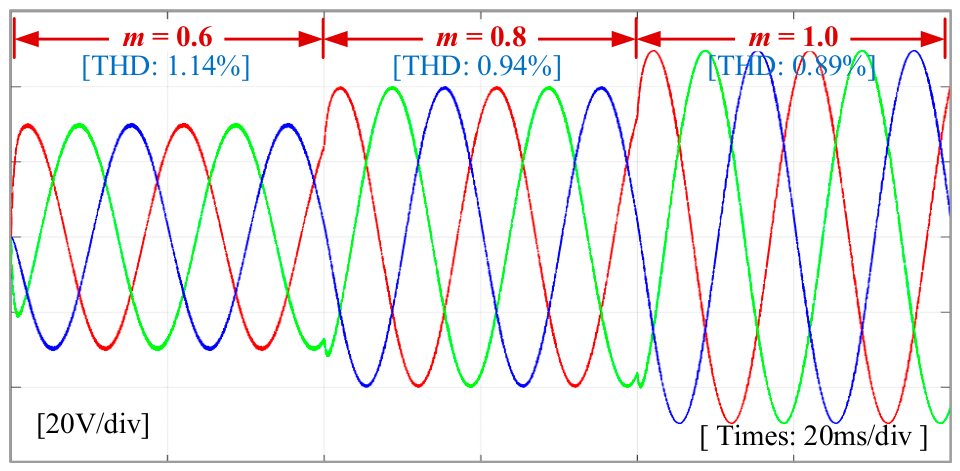
Figure 13, Figure 14 and Figure 15 present additional simulation results obtained using carrier-based comparison modulation for other conditions. Figure 13 shows the output current and corresponding sinusoidal voltage waveforms of phase-a under different switching frequencies. As the switching frequency increases, the number of current pulses per line cycle increases, leading to a higher pulse density; concurrently, voltage ripple decreases progressively, thereby enhancing the quality of the output voltage waveform. Figure 14 displays the three-phase output voltage waveforms under different modulation indexes. Under step changes in the reference current, the transient response of the output voltage exhibits a rapid and well-damped tracking behavior, confirming the system’s effective dynamic adaptation to modulation index variations. Figure 15 displays the acquired voltage and current waveforms of the CSI under varying load conditions. For systematic comparison, the load impedance magnitude is held constant at 10 Ω, and the power factor is progressively adjusted by tuning the resistance and inductance values of the series-connected R-L load to achieve different operating conditions. All other system parameters, including switching frequency, DC-link current, and control strategy, were kept identical across test cases; therefore, the current pulse characteristics remained invariant. Furthermore, the waveform quality of the output voltage exhibits only negligible fluctuation in response to variations in load. However, as the power factor decreased, the phase displacement between voltage and current increased as expected.
Figure 13.
Comparison with different switching frequency values for CBPWM modulation: (a) 5 kHz; (b) 10 kHz; (c) 20 kHz.
Figure 14.
Transient response to the step changes in modulation index.
Figure 15.
Comparison with different power factors for CBPWM scheme. (a) Power factor: 0.8; (b) power factor: 0.5; (c) power factor: 0.2.
6. Experimental Results
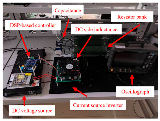
To further validate the equivalence of both modulation methods, experiments were conducted on the experimental platform shown in Figure 16. The platform comprised a DSP-based controller (TMS320F28335), a three-phase current-source inverter, and a star-connected load with three 35 μF capacitors and three 10 Ω resistors, as detailed circuit schematic diagram in Figure 1 and detailed parameters in Table 3.
Figure 16.
Experimental platform.
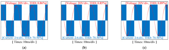
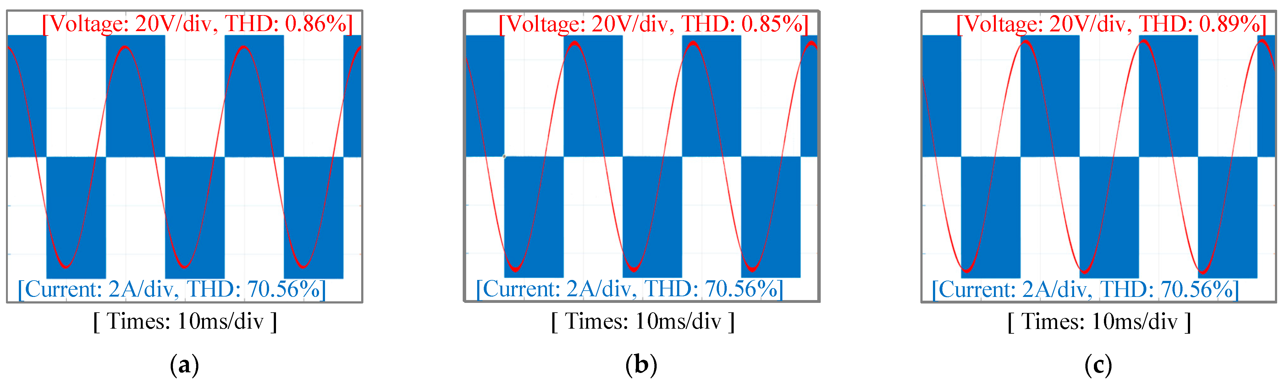
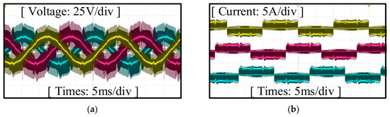
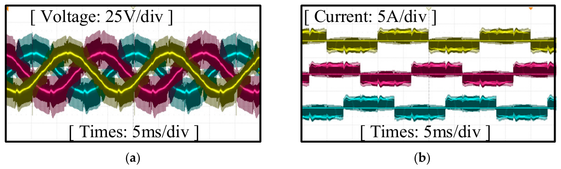
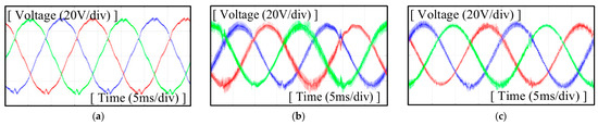
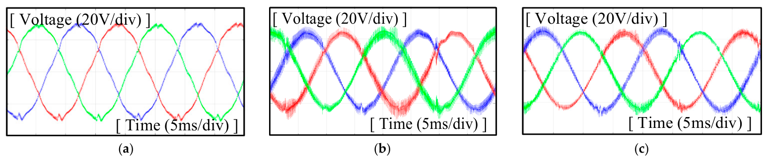
Figure 17 presents the raw experimental waveforms of line-to-line voltage and phase current obtained under the following conditions: modulation index m = 0.85, carrier switching frequency fs = 20 kHz, and DC-side inductance Ld = 0.5 mH. These parameters match the simulation conditions described earlier. The acquired line-to-line voltage signal is post-processed using MATLAB digital filtering to produce the waveform displayed in Figure 18a. To mitigate current-source interruption risks during bridge-leg commutation, we implemented an enhanced switching strategy: during PWM transition sectors, one complementary switch pair (upper and bottom devices) maintains continuous conduction throughout the entire PWM cycle. This modification introduces minor waveform distortions near voltage peaks, as visible in the experimental results. Nevertheless, the measured voltage waveform demonstrates close agreement with the simulation. To validate more operating conditions such as DPWM, experiments were also conducted for both k = 0 and k = 1 cases, as shown in Figure 18b,c. This experimental finding also demonstrates that the proposed carrier-based modulation scheme remains feasible for DPWM applications.
Figure 17.
Experimental results for the output voltage and current. (a) Line-to-line voltage; (b) phase current.
Figure 18.
Line-to-line voltage after filtering ringing. (a) Continuous PWM; (b) DPWM (k = 0); (c) DPWM (k = 1).
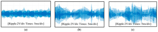
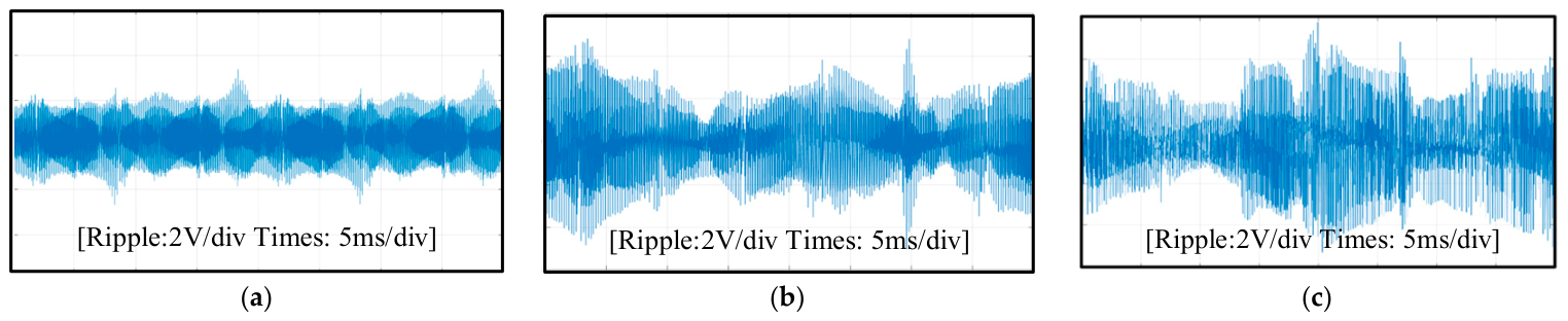
Figure 19 further presents the high-frequency voltage ripple characteristics of the output voltage. Additionally, through program calculation, the THD of the output voltage is 4.94%, which is slightly higher than the simulation result under the same conditions. These experimental results conclusively validate the feasibility of the proposed CBPWM technique for CSIs. Through the experimental results, it can be concluded that the proposed carrier-based modulation technique for current source inverter proposed in this paper is feasible.
Figure 19.
Voltage ripple after filtering ringing. (a) Continuous PWM; (b) DPWM (k = 0); (c) DPWM (k = 1).
The primary contribution of this paper is the proposal of a CBPWM method that achieves functional equivalence to conventional SVPWM while offering significantly reduced computational complexity and enhanced implementation feasibility. As summarized in Table 4, both methods deliver identical steady-state and dynamic output performance, as verified through comprehensive simulation and experimental validation. Nevertheless, CBPWM reduces the required instruction cycles from 8,080 (SVPWM) to 1,568, representing an approximately 80.6% reduction. This comparison is conducted under identical conditions using Texas Instruments Code Composer Studio (CCS) on a C2000™ TMS320F28335 DSP operating at 150 MHz. Consequently, the corresponding computation times are 53.9 μs for SVPWM and 10.5 μs for CBPWM. The substantial computational saving afforded by CBPWM enables either the allocation of surplus processing capacity to advanced control algorithms (e.g., model predictive control or adaptive observers) or the adoption of higher switching frequencies without compromising real-time execution integrity.
Table 4.
Calculated burden for different modulation strategies.
7. Conclusions
This paper establishes the theoretical equivalence between two modulation strategies for CSIs: SVPWM and CBPWM. Specifically, by injecting a precisely defined zero-sequence current component into the three-phase reference currents, the vector synthesis procedure inherent to SVPWM, traditionally achieved through complex geometric decomposition and trigonometric computations, is equivalently achieved using straightforward carrier-comparison logic. The design of a CBPWM scheme that replicates the performance and switching sequence of the conventional seven-segment, center-symmetric SVPWM is rigorously formulated and validated. The modulated signal is compared with the triangular carrier to generate three two-level PWM signals. By pairwise subtracting the two-level PWM signals, the three-level PWM is obtained. When the three-level PWM equals 1, the corresponding upper switch is turned on; when the three-level PWM equals −1, the corresponding lower switch is activated. The CBPWM scheme generates all the switching states, duty cycles, and switching sequences that are based on carrier comparison and simple calculation, which is equivalent to the SVPWM scheme. Comprehensive test validation confirms the theoretical equivalence of the two modulation approaches and quantitatively demonstrates the substantial computational efficiency advantage of CBPWM over SVPWM.
Author Contributions
Conceptualization, M.Z. and J.C.; methodology, M.Z. and J.C.; software, M.Z.; validation, M.Z. and J.C.; formal analysis, M.Z.; investigation, M.Z.; resources, J.C.; data curation, M.Z.; writing—original draft preparation, M.Z.; writing—review and editing, J.C.; visualization, J.C.; supervision, J.C.; project administration, J.C.; funding acquisition, J.C. All authors have read and agreed to the published version of the manuscript.
Funding
This research was funded in part by Basic Research Program of Jiangsu, grant number BK20230323, and in part by the General Project of Basic Science (Natural Science) Research of Higher Education Institutions in Jiangsu Province, grant number 23KJB470012.
Data Availability Statement
The original contributions presented in the study are included in the article; further inquiries can be directed to the corresponding authors.
Conflicts of Interest
The authors declare no conflicts of interest. The funders had no role in the design of the study; in the collection, analyses, or interpretation of data; in the writing of the manuscript; or in the decision to publish the results.
References
- Gupta, K.K.; Ranjan, A.; Bhatnagar, P.; Sahu, L.K.; Jain, S. Multilevel Inverter Topologies with Reduced Device Count: A Review. IEEE Trans. Power Electron. 2016, 31, 135–151. [Google Scholar] [CrossRef] [Scilit]
- Liu, P.; Wang, Z.; Xu, Y.; Zou, Z.; Deng, F.; Li, Y. Improved harmonic profile for high-power PWM current-source converters with modified space-vector modulation schemes. IEEE Trans. Power Electron. 2021, 36, 11234–11244. [Google Scholar] [CrossRef] [Scilit]
- Giraldo, E.; Garces, A. An adaptive control strategy for a wind energy conversion system based on PWM-CSC and PMSG. IEEE Trans. Power Syst. 2014, 29, 1446–1453. [Google Scholar] [CrossRef] [Scilit]
- Liu, P.; Wang, Z.; Song, Q.; Xu, Y.; Cheng, M. Optimized SVM and remedial control strategy for cascaded current-source-converters-based dual three-phase PMSM drives system. IEEE Trans. Power Electron. 2020, 35, 6153–6164. [Google Scholar] [CrossRef] [Scilit]
- Migliazza, G.; Buticchi, G.; Carfagna, E.; Lorenzani, E.; Madonna, V.; Giangrande, P.; Galea, M. DC Current Control for a Single-Stage Current Source Inverter in Motor Drive Application. IEEE Trans. Power Electron. 2021, 36, 3367–3376. [Google Scholar] [CrossRef] [Scilit]
- Wang, X.; Wei, T.; Wang, R.; Hu, Y.; Liu, S. A Novel Carrier-Based PWM Without Narrow Pulses Applying to High-Frequency Link Matrix Converter. IEEE Access 2020, 8, 157654–157662. [Google Scholar] [CrossRef] [Scilit]
- Yang, H.-K.; Park, J.-W. Sawtooth-Carrier-Based Pulse width Modulation Method for Quasi-Z-Source Inverter with Zero-Voltage-Switching Operation to Reduce Harmonic Distortion and Inductor Current Ripple. IEEE Trans. Ind. Electron. 2021, 68, 916–924. [Google Scholar] [CrossRef] [Scilit]
- Houldsworth, J.A.; Grant, D.A. The use of harmonic distortion to increase the output voltage of a three-phase PWM inverter. IEEE Trans. Ind. Appl. 1984, 20, 1224–1228. [Google Scholar] [CrossRef] [Scilit]
- Li, X.; Kennel, R. General Formulation of Kalman-Filter-Based Online Parameter Identification Methods for VSI-Fed PMSM. IEEE Trans. Ind. Electron. 2021, 68, 2856–2864. [Google Scholar] [CrossRef] [Scilit]
- Arumalla, R.T.; Figarado, S.; Panuganti, K.; Harischandrappa, N. Selective Lower Order Harmonic Elimination in DC-AC Converter Using Space Vector Approach. IEEE Trans. Circuits Sys. II Express Briefs 2021, 68, 2890–2894. [Google Scholar] [CrossRef] [Scilit]
- Ostadrahimi, A.; Bifaretti, S. A Simplified Multilevel Space Vector Pulse Width Modulation (SVPWM) Based on Boundary Lines, Including Overmodulation Zone. IEEE Open J. Ind. Appl. 2023, 4, 215–226. [Google Scholar] [CrossRef] [Scilit]
- Xing, X.; Li, X.; Gao, F.; Qin, C.; Zhang, C. Improved space vector modulation technique for neutral-point voltage oscillation and common-mode voltage reduction in three-level inverter. IEEE Trans. Power Electron. 2019, 34, 8697–8714. [Google Scholar] [CrossRef] [Scilit]
- Nguyen, T.-T.; Cha, H.; Do, D.-T.; Akbar, F. Modified SVPWM for Three-Phase Six-Switch Switching-Cell Current Source Inverter. IEEE Trans. Power Electron. 2022, 37, 14820–14830. [Google Scholar] [CrossRef] [Scilit]
- Pradeepa, S.; Kumar, S.; Prakash, G. Adoption of SVPWM Technique to CSI and VSI. In Proceedings of the 2018 3rd International Conference for Convergence in Technology (I2CT), Pune, India, 6–8 April 2018; pp. 1–6. [Google Scholar] [CrossRef] [Scilit]
- Sun, Q.; Wang, Z.; Sharkh, S.M.; Hao, W. A Flexible and Decoupled Space Vector Modulation Scheme with Carrier-Based Implementation for Multilevel Converters. IEEE Trans. Power Electron. 2023, 38, 8135–8149. [Google Scholar] [CrossRef] [Scilit]
- Shen, Z.; Li, Z.; Zhou, D.; Zou, J.; Jiang, D. A Computationally Efficient Carrier-Based PWM Strategy for Asymmetrical Six-Phase Motor Drive of Electric Vehicle with Unified Zero-Sequence Signal. IEEE Trans. Transp. Electrif. 2024, 10, 7191–7202. [Google Scholar] [CrossRef] [Scilit]
- Deng, Y.; Teo, K.H.; Duan, C.; Habetler, T.G.; Harley, R.G. A Fast and Generalized Space Vector Modulation Scheme for Multilevel Inverters. IEEE Trans. Power Electron. 2014, 29, 5204–5217. [Google Scholar] [CrossRef] [Scilit]
- Wang, H.; Zhang, J.; Zhu, C.; Cai, X.; Zhu, M. DC-link current optimal control of current source converter in DFIG. CPSS Trans. Power Electron. Appl. 2021, 6, 127–135. [Google Scholar] [CrossRef] [Scilit]
- Li, X.; Sun, Y.; Jiang, L.; Wang, H.; Liu, Y.; Su, M. Common-Mode Circuit Analysis of Current-Source Photovoltaic Inverter for Leakage Current and EMI. IEEE Trans. Power Electron. 2023, 38, 7156–7165. [Google Scholar] [CrossRef] [Scilit]
- Rahman, M.M.; Mohamed, Y.A.-R.I. Dynamic Analysis and Active Stabilization of a Utility-Scale Grid-Connected Current-Source Inverter-Based PV System Considering Source Dynamics. IEEE Trans. Power Syst. 2022, 37, 4590–4604. [Google Scholar] [CrossRef] [Scilit]
- Narasimhan, S.; Bhattacharya, S.; Zargari, N.R. Comparison of a 10 kV SiC Current Switch With two 6.5 kV Series Connected Si SGCTs for Medium Voltage Current Source Converter Applications. IEEE Trans. Ind. Appl. 2025, 61, 370–382. [Google Scholar] [CrossRef] [Scilit]
- Richu, S.C.; Rajeevan, P.P. A Load Commutated Multilevel Current Source Inverter Fed Open-End Winding Induction Motor Drive with Regeneration Capability. IEEE Trans. Power Electron. 2020, 35, 816–825. [Google Scholar] [CrossRef] [Scilit]
- Guo, X.; Xu, D.; Guerrero, J.M.; Wu, B. Space Vector Modulation for DC-Link Current Ripple Reduction in Back-to-Back Current-Source Converters for Microgrid Applications. IEEE Trans. Ind. Electron. 2015, 62, 6008–6013. [Google Scholar] [CrossRef] [Scilit]
- Xing, L.; Wei, Q.; Li, Y.; Liu, Y.-F. Phase-Shifting SPWM-Based Modulation for Single-Source Five-Level Current Source Inverter. IEEE Trans. Power Electron. 2025, 40, 10343–10348. [Google Scholar] [CrossRef] [Scilit]
- Yang, S.; Zheng, P.; Sui, Y.; Tong, C.; Wang, M. Carrier-Based PWM Technique and Extended State Observer-Based Current Control Scheme for Current-Source Inverter-Fed Five-Phase PMSM Drives. IEEE Trans. Ind. Electron. 2024, 71, 6635–6646. [Google Scholar] [CrossRef] [Scilit]
- Zhou, K.; Wang, D. Relationship between space-vector modulation and three-phase carrier-based PWM: A comprehensive analysis. IEEE Trans. Ind. Electron. 2002, 49, 186–196. [Google Scholar] [CrossRef] [Scilit]
- Surana, P.; Vivek, R.S.; Vaidika, T.P.; Gopakumar, K.; Umanand, L. Synthesis of a Modulating Waveform for a Carrier-Based Dodecagonal Space Vector PWM Signal Generation for a Split-Phase Induction Motor Drive. IEEE Trans. Ind. Electron. 2024, 71, 15415–15423. [Google Scholar] [CrossRef] [Scilit]
- López, Ó.; Alvarez, J.; Yepes, A.G.; Baneira, F.; Perez-Estevez, D.; Freijedo, F.D.; Doval-Gandoy, J. Carrier-Based PWM Equivalent to Multilevel Multiphase Space Vector PWM Techniques. IEEE Trans. Ind. Electron. 2020, 67, 5220–5231. [Google Scholar] [CrossRef] [Scilit]
- Qiu, Z.; Zhang, Y.; Xiong, J.; Gao, N.; Lin, S.; Zhou, L. A Phase-Shift PWM Based Zero-Sequence Voltage Injection Method for Neutral-Point Potential Balance of Five-Level ANPC Converters. In Proceedings of the 2021 IEEE 12th Energy Conversion Congress & Exposition-Asia (ECCE-Asia), Singapore, 24–27 May 2021; pp. 670–675. [Google Scholar] [CrossRef] [Scilit]
- Adrien, B.; Ghanes, M.; Maurice, F.; Abdelkader, B.; Jean-Pierre, B. A New PWM Control based on an Optimized Zero Sequence Component injection: Application in a Two-Level Inverter. In Proceedings of the 47th Annual Conference of the IEEE Industrial Electronics Society, Toronto, ON, Canada, 13–16 October 2021; pp. 1–6. [Google Scholar] [CrossRef] [Scilit]
- Chen, F.; Qiao, W.; Wang, H.; Qu, L. A Simple Zero-Sequence Voltage Injection Method for Carrier-Based Pulse-width Modulation of the Three-Level NPC Inverter. IEEE J. Emerg. Sel. Top. Power Electron. 2021, 9, 4687–4699. [Google Scholar] [CrossRef] [Scilit]
- Cheng, R.; He, Y.; Lei, C.; Wang, Y.; Liu, J. Research on Realizing Space Vector Equivalent Modulation Output by Dual Carrier Modulation of Current Source Inverter. IEEE Trans. Power Electron. 2021, 36, 8494–8505. [Google Scholar] [CrossRef] [Scilit]
- Pujol, P.B.; Dòria-Cerezo, A.; Griñó, R. Averaged Models and Analysis of a Three-Phase CSI as a Dual of a Three-Phase VSI. In Proceedings of the 2024 IEEE International Conference on Industrial Technology (ICIT), Bristol, UK, 25–27 March 2024; pp. 1–6. [Google Scholar] [CrossRef] [Scilit]



Disclaimer/Publisher’s Note: The statements, opinions and data contained in all publications are solely those of the individual author(s) and contributor(s) and not of MDPI and/or the editor(s). MDPI and/or the editor(s) disclaim responsibility for any injury to people or property resulting from any ideas, methods, instructions or products referred to in the content. |
© 2026 by the authors. Licensee MDPI, Basel, Switzerland. This article is an open access article distributed under the terms and conditions of the Creative Commons Attribution (CC BY) license.