


Abstract
This article explores the high-frequency characteristics of gallium nitride (GaN) power-switching devices and evaluates their application performance using a double-pulse test (DPT) circuit model. With the increasing adoption of GaN power-switching devices in high-performance and miniaturized electronic products, their low junction capacitance makes them highly suitable for high-frequency applications. However, parasitic inductance in the power loop can introduce resonance phenomena, impacting system stability and switching performance. To address this, this study integrates the parasitic parameters of printed circuit boards (PCBs) with the nonlinear junction capacitance characteristics of GaN devices. Finite element analysis (FEA) is employed to extract PCB parasitic inductance values and analyze their effects on GaN power-switching behavior. The findings indicate that precise extraction and analysis of parasitic inductance are critical for optimizing the performance of GaN switching devices. Additionally, this study investigates mitigation strategies to minimize parasitic inductance, ultimately enhancing GaN device design and reliability. The insights from this research provide valuable guidance for the development of GaN power devices in high-frequency applications.
1. Introduction
Gallium nitride (GaN) power-switching devices, resulting from advancements in power semiconductor technology, provide effective solutions for converters, achieving higher frequency and power density objectives. Contrary to conventional silicon power components nearing their operational limits, the incorporation of GaN and silicon carbide (SiC) in power converters has notably improved power density and efficiency, surpassing traditional silicon metal-oxide-semiconductor field-effect transistors (MOSFETs). In the domain of wide-bandgap power components, silicon-based GaN lateral heterojunction power components gain prominence due to their fabrication on cost-effective, large-sized silicon substrates [1,2,3,4]. When analyzing GaN power-switching devices, the initial focus lies in the simplest double-pulse testing (DPT) circuit. However, a critical aspect often overlooked is the precise examination of switch devices in basic circuits. Various factors, including understanding the component’s operation, designing peripheral circuit elements, and considering printed circuit board (PCB) layouts, should also receive remarkable attention. Understanding how to interpret the contributions of diverse factors is imperative when scrutinizing waveforms.
The existing literature mainly focuses on the loss analysis of switching components, with limited attention paid to the parasitic inductance parameters of the surrounding PCB and the challenges associated with further reducing these parasitic parameters. Only a few analyses have been carried out on effectively capturing parasitic inductance or which frequency range should be targeted. Material theory suggests that copper properties are affected by the skin effect at both low and high frequencies, influencing its skin depth. As a result, the observed parasitic inductance and resistance may vary. This article will explore in detail how to choose an appropriate frequency range for capturing parasitic inductance [5,6,7].
GaN power-switching devices introduce additional complexities to the PCB layout as higher power switch frequencies are achieved [8,9,10]. In practical circuit applications, GaN structures exhibit relatively moderate junction capacitance, typically within the range of a few picofarads. However, parasitic inductance in PCB traces can escalate to the nanohenry range, leading to resonance between the parasitic inductance of PCB and the junction capacitance of GaN. This resonance may pose risks, exceeding the rated voltage of the component, thereby increasing the complexities of the PCB layout. This article primarily focuses on the basic DPT circuit, exploring strategies to mitigate parasitic inductance issues, with the anticipation that this conceptual framework can serve as a reference for diverse applications [11,12,13,14].
To achieve a comprehensive analysis, this study follows a structured approach:
A model is developed for DPT to establish key concepts in power-switching device analysis, including resonance conditions in the power loop, switching device junction capacitance, PCB parasitic inductance, and the use of fast Fourier transform (FFT) analysis on an approximated square wave to assess resonance magnitude. The turn-on and turn-off behavior of GaN power-switching devices is also examined to build a strong theoretical foundation [15].
Finite element analysis (FEA) simulations are performed on the PCB to extract parasitic inductance parameters from the main power loop. The extracted model is then validated through experimental tests to ensure accuracy. This approach provides deeper insights into factors affecting measured waveforms, reducing the risk of misinterpretations—especially in identifying resonance features during testing [16].
A detailed examination of GaN power-switching device modeling within DPT circuits is conducted, focusing on interactions between PCB parasitic inductance and GaN junction capacitance. Methods for extracting parasitic inductance and strategies for mitigating its effects are discussed. Experimental DPT circuit results validate the accuracy of the extracted model, further confirming the effectiveness of FEA simulations in determining PCB parasitic inductance parameters.
Therefore, this study aims to enhance our understanding of power electronics design, ultimately improving the performance and reliability of GaN power-switching devices. By addressing critical challenges related to PCB parasitic inductance, this work contributes to the advancement of high-frequency power conversion and the optimization of GaN-based power system designs.
2. Characteristic of Oscillations of Power Loops on Power E-GaN Switching Applications
Oscillations during switch transitions are primarily caused by the interaction between the switch’s parasitic capacitance (Coss) and the PCB’s parasitic inductance (Lt). This section first provides a brief explanation of parasitic capacitance in E-GaN power-switching devices; then, an introduction into the principles and operation of the DPT circuit is provided. Based on these foundations, the analysis then extends to the effects of parasitic inductance on the circuit. This discussion enhances our understanding of the cause of resonance.
2.1. The Junction Capacitance of E-GaN
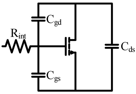
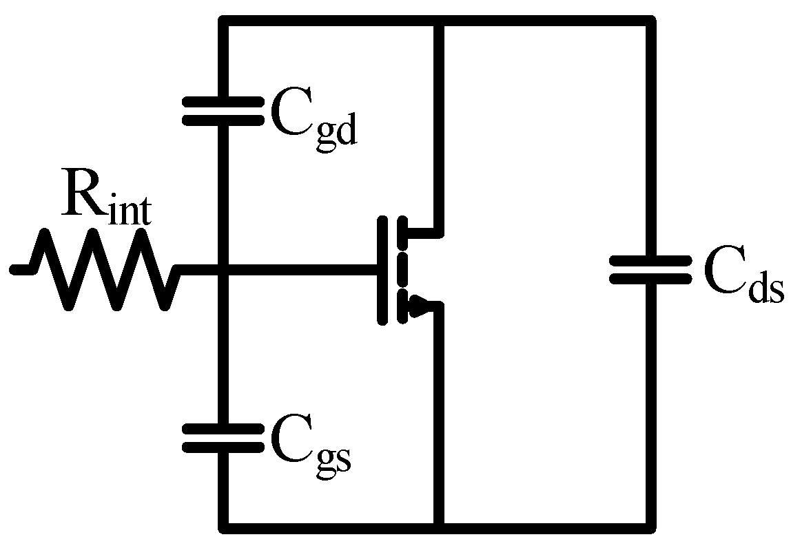
A detailed exploration of crucial parameters associated with GaN power-switching devices encompassing factors such as junction capacitance and nonlinear transconductance is provided. GaN power-switching devices share characteristics with general MOSFETs, featuring significant parameters such as Cds, Cgd, Cgs, and Rint. To elaborate further, the three intrinsic capacitors in these devices are defined as follows: Ciss, the input capacitance, is obtained by totaling the gate-source capacitance (Cgs) and gate-drain capacitance (Cgd), representing the overall capacitance of GaN as observed from the input. Coss, the output capacitance, is obtained by adding the drain-source capacitance (Cds) and the gate-drain capacitance (Cgd), representing the total capacitance on the output side. Crss, the reverse transfer capacitance, is synonymous with the gate-drain capacitance (Cgd). Their relationships between Cds, Cgd, and Cgs are illustrated in Figure 1, depicting the junction capacitance of a GaN power-switching device.
Figure 1.
Junction capacitance of a GaN power-switching device.
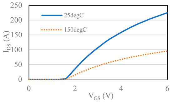
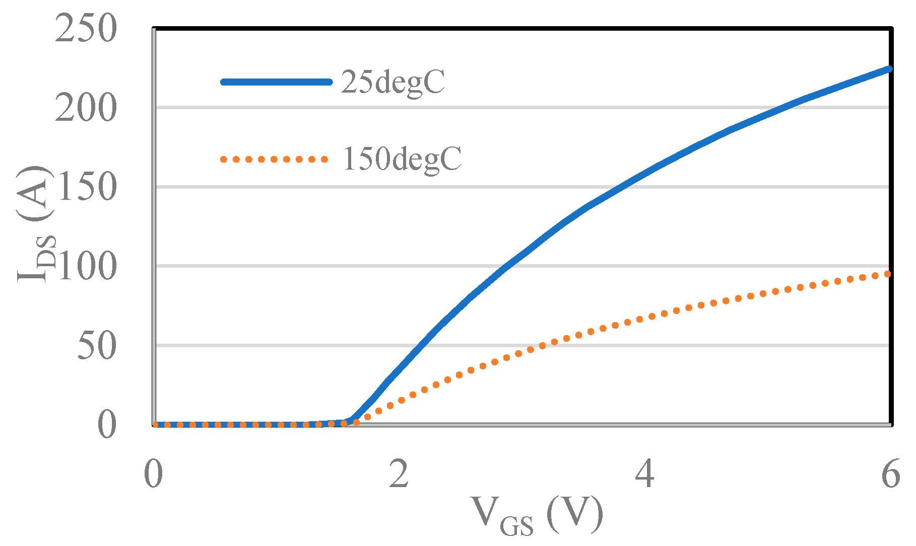
A curve-fitting method is used to extract the junction capacitance values at each bias voltage. These extracted values are applied in the mathematical model. The curve-fitting methods are used to capture trends and patterns in the data and to estimate junction capacitance values at specific voltage points. Such an analysis contributes to understanding the performance characteristics of junction capacitance, providing valuable information for further engineering design or optimization. The transconductance gm plays a crucial role in GaN power-switching devices, with its significance underscored by its response to temperature variations. The transconductance diminishes as temperatures increase, resulting in a smaller gm. Consequently, the Miller plateau becomes wider. This study seeks to establish a mathematical model specifically at room temperature. The transfer characteristic of GaN is nonlinear, as shown in Figure 2 [17].
Figure 2.
Transfer characteristics of GS66516T at Vds = 10 V.
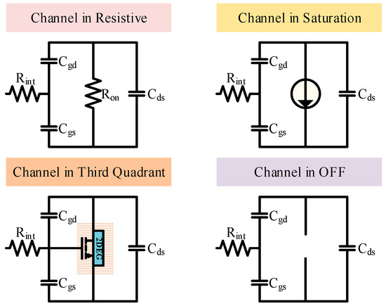
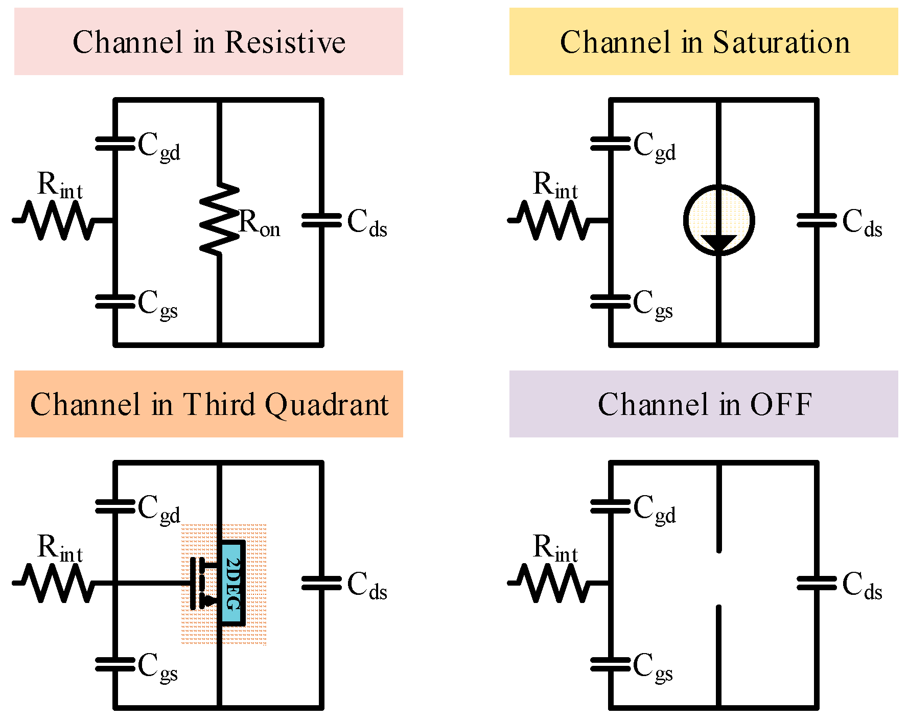
GaN power-switching devices exhibit four distinct operating modes: OFF, the resistive region, saturation region, and third quadrant region (reverse operation region). In the OFF mode, the switch is completely disconnected, with only junction capacitance in operation. The resistive region mode signifies that the switch is in the resistance operating region, indicating an open state. The saturation region mode reflects the state during the transition process. Finally, the third region operating mode denotes that the switch is actively performing operations in the third region, distinguishing itself from the typical MOSFET and silicon carbide (SiC) operating modes. Figure 3 illustrates the four states, providing a clear depiction of the characteristics of the GaN switch in various operating modes [18].
Figure 3.
Four operational states of GaN.
2.2. Modeling of DPT Circuit
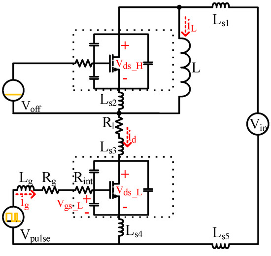
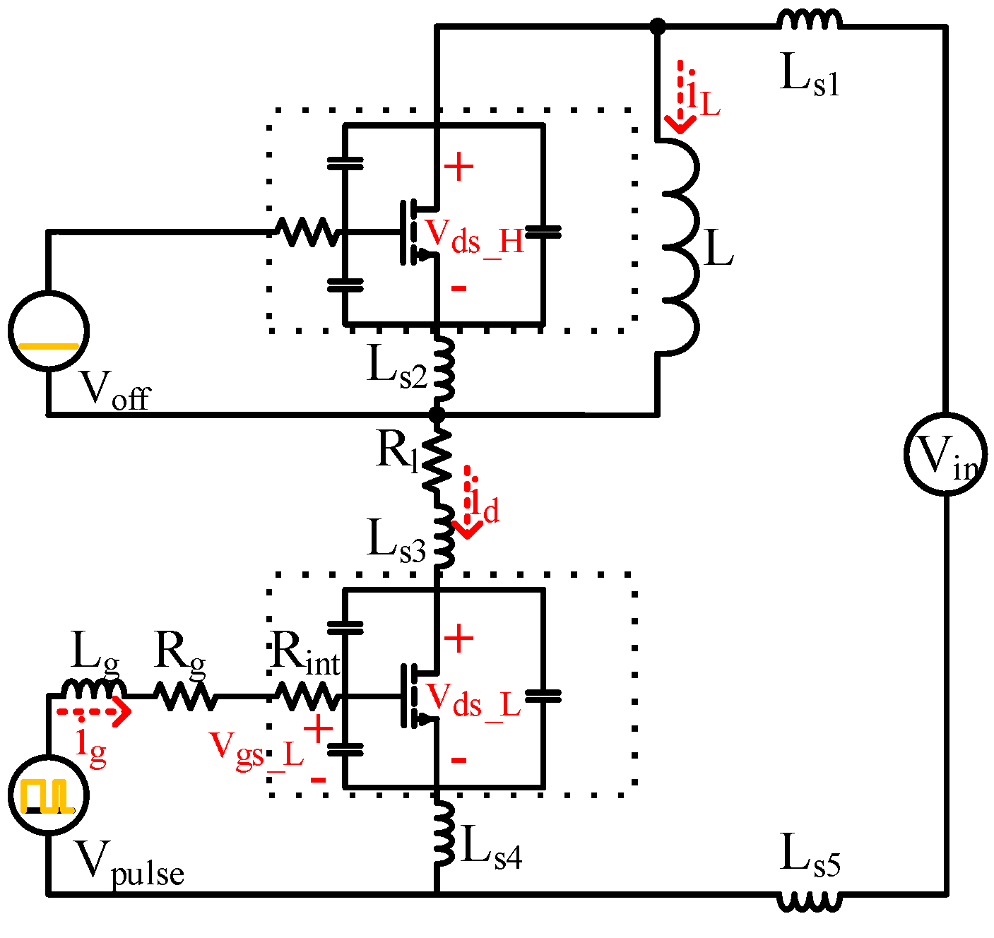
Several articles have extensively explored the DPT intervals. In this specific study, the DPT circuit intervals are reexamined by incorporating a GaN power-switching device. Clear distinctions become evident when compared with SiC power-switching devices, especially during the turn-off time of states 6 and 7. Following thorough analyses of each state, the subsequent step involves deriving and solving differential equations, leading to the mathematical representation of waveforms. The modeling and experiments are based on the DPT circuit, as illustrated in Figure 4. The model considers the package and external circuit, parasitic inductances, internal resistances, and junction capacitance. In addition, Vin represents the main power loop for DC voltage. A voltage value of zero is applied to the high-side GaN, drive voltage pulses are applied to the low-side GaN, and the inductor L supports the load current.
Figure 4.
DPT circuit.
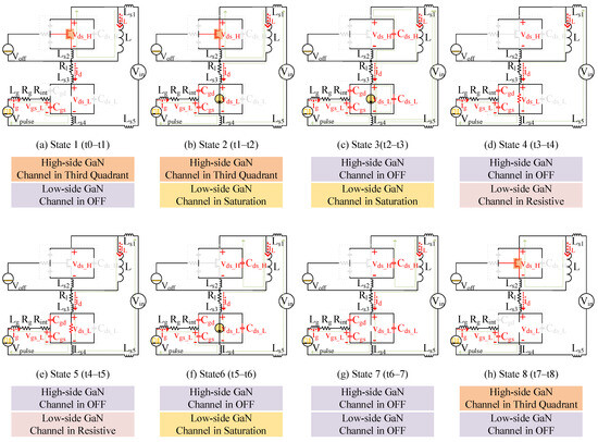
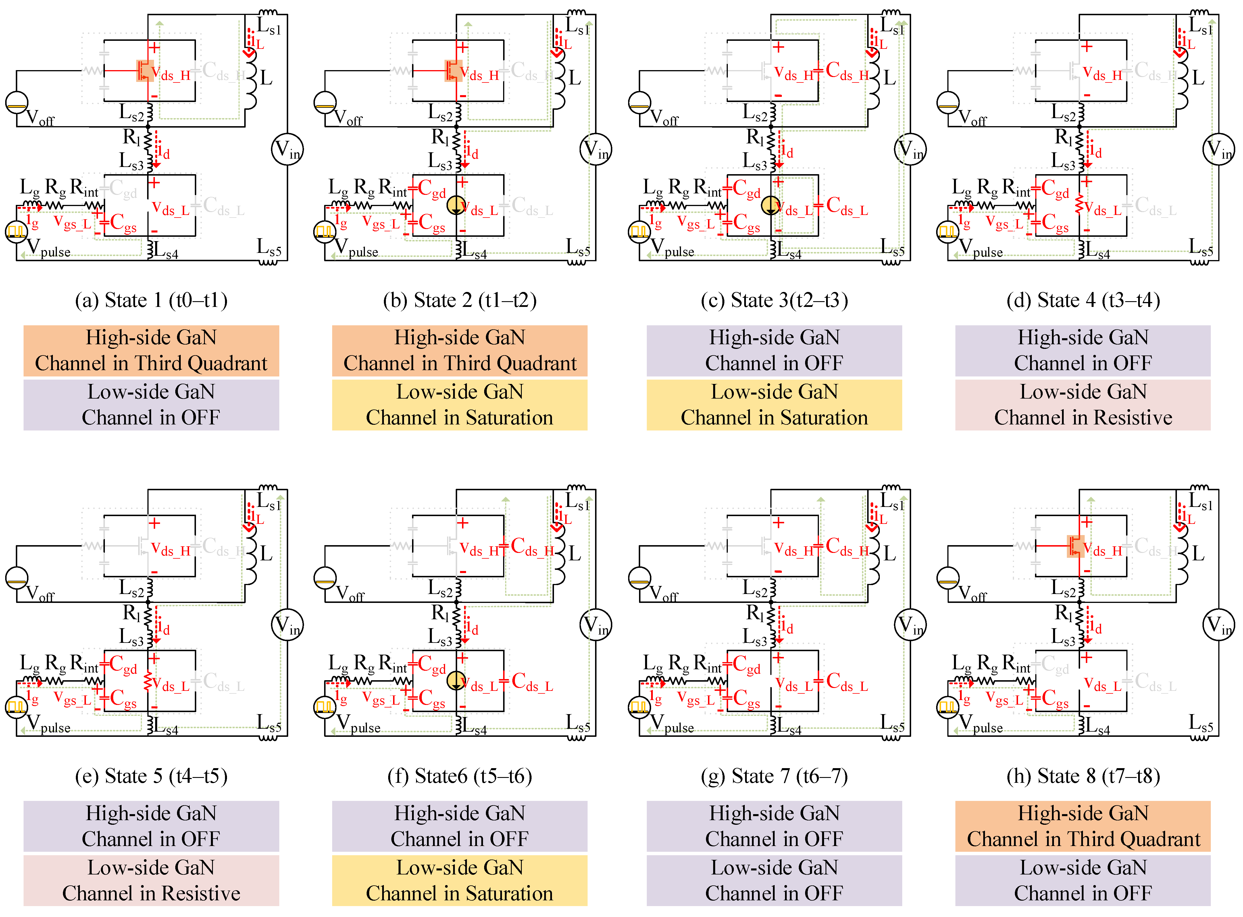
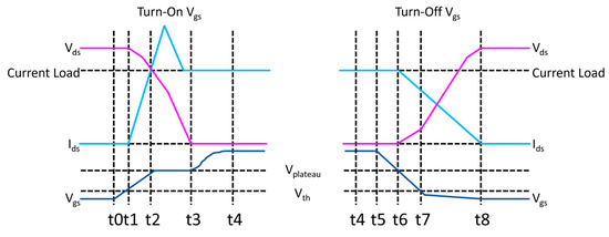
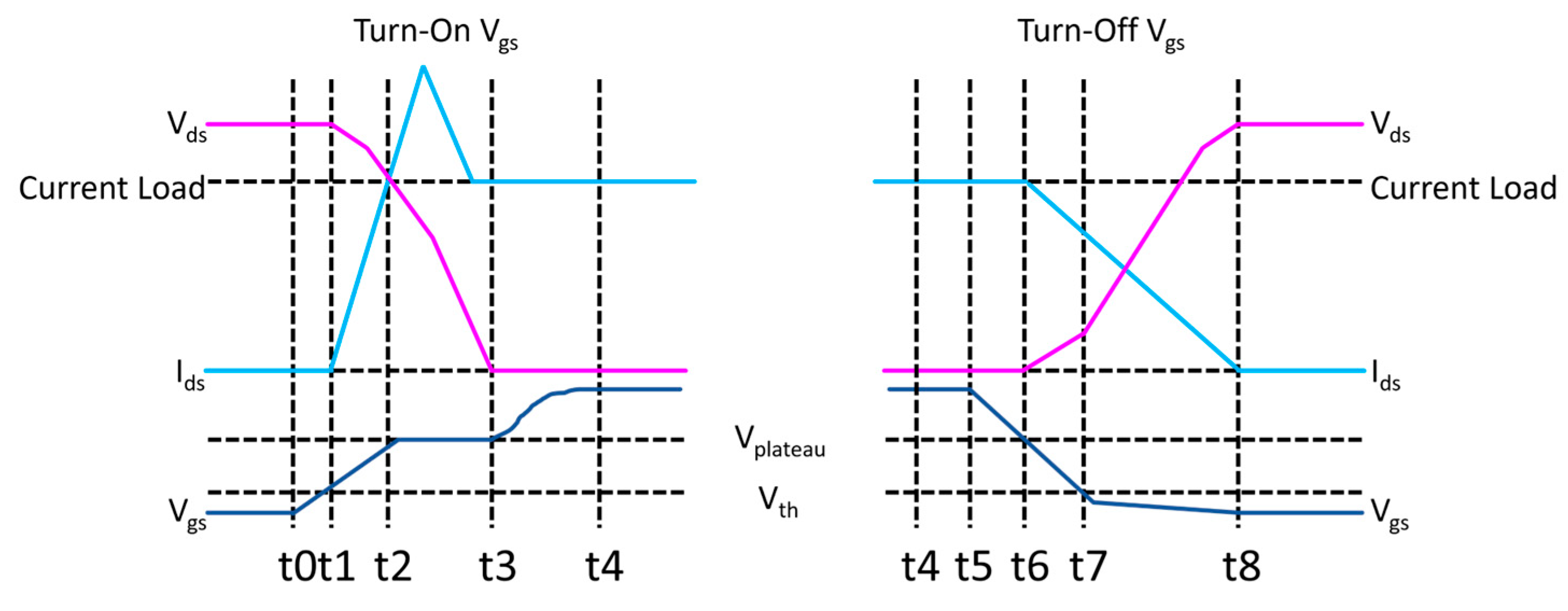
To obtain a comprehensive understanding of the model, waveforms at each state are examined, and temporal considerations are incorporated to engage each junction capacitor of GaN in resonance within those states. This systematic approach seeks to provide a balanced perspective on the behavioral dynamics of each constituent element within every state, promoting a nuanced understanding of the overall dynamic processes inherent in the entire system, as shown in Figure 5 and Figure 6.
Figure 5.
Operational ON/OFF switching states.
Figure 6.
Timing diagram of ON/OFF switching states.
2.2.1. Turn-On Model
Prior to turning on the GaN power device, the inductor current iL flows through the third area of the high-side GaN power device, and the voltage Vin is applied. The turn-on transition can be divided into four states as follows:
State 1 (t0–t1) [Figure 5a]: When the gate voltage (Vpulse) is applied, the gate current (ig) begins charging the Cgs of the low-side GaN. At this point, with Vpulse < Vth (threshold voltage), the 2D electron gas (2DEG) in the low-side GaN is in the off state, resulting in no drain-to-source current. Then, the load current (iL load) flows through the high-side GaN, which operates in the third quadrant. The equivalent circuit in state 1 can be represented as Equations (4)–(8):
where .
State 2 (t1–t2) [Figure 5b]: When the gate voltage (Vpulse) increases above the threshold, the low-side GaN enters the saturation region, which is Vgs_L > Vgs(th); the impedance of the 2DEG starts to decrease; and the drain current, id, starts to rise. During this state, Vds_L decreases due to di/dt-induced voltages across L and Lt. The load current (iL) continues to flow through the high-side GaN, which operates in the third quadrant. The equivalent circuit in state 2 can be represented as Equations (5) and (9)–(11):
State 3 (t2–t3) [Figure 5c]: After the current is completely commutated to the low-side GaN, the high-side GaN leaves the third quadrant of the 2DEG and blocks the DC voltage, thereby initiating the voltage reduction in the low-side GaN. At this moment, the Cgd of the low-side GaN is charged. At this point, a Miller voltage is achieved, that is, Vgs reaches Vplateau. During the voltage reduction period, the output capacitance (Cds + Cgd) in the low-side GaN discharges into the 2DEG of the saturated region, resulting in energy loss. Simultaneously, the Cds_H of the high-side GaN is charged with current from the DC bus and decoupling capacitors. The equivalent circuit in state 3 can be represented as Equations (5), (9), (11) and (12):
State 4 (t3–t4) [Figure 5d]: Once the switch node voltage reaches the designated level, the device will transition to the Ohmic region, marking the completion of the conduction transient. The equivalent circuit for state 4 can be represented as Equations (5), (9), (11) and (13):
2.2.2. Turn-Off Model
Prior to turning off the GaN transistor, the inductor current iL passes through the Rdson of the low-side switch. The turn-off transition can be segmented into four states, each of which is analyzed in the subsequent sections.
State 5 (t4–t5) [Figure 5e]: The current load (iL) remains in the ohmic region of the low-side GaN’s 2DEG as the gate voltage (Vpulse) decreases from the driving voltage to the Miller voltage (Vplateau). Simultaneously, the gate current (ig) discharges the Cgs of the low-side GaN. No current flows into either Cds of the GaN.
State 6 (t5–t6) [Figure 5f]: When the gate voltage reaches the Miller voltage, the impedance of the low-side GaN’s 2DEG rises, surpassing the Rdson and entering the saturation region. In addition, the load current begins to discharge into the Cds of the high-side GaN. Most losses occur in this state, and the Cgd of the low-side GaN is discharged. The equivalent circuit in state 6 can be represented as Equations (5), (9), (11) and (14).
State 7 (t6–t7) [Figure 5g]: When the gate voltage falls below the threshold value, the 2DEG of the low-side GaN turns off completely, preventing any current from flowing through. The load current is subsequently redirected to charge the Cds of the low-side GaN. During this state, no additional resistive losses occur; only lossless displacement is observed, including the energy stored in the Cds of the low-side GaN. The equivalent circuit in state 7 can be represented as Equations (5), (9), (11) and (15):
State 8 (t7–t8) [Figure 5h]: After the completion of charge displacement, voltage rise and current fall are achieved, enabling the entire load current to traverse the 2DEG in a diode-like mode within the high-side GaN. The equivalent circuit in state 8 can be expressed as Equations (4)–(8).
3. The Parasitic Inductance Lt of the DPT Circuit
When scrutinizing GaN switching components, the primary focus is on the junction capacitance within the GaN and the parasitic inductance generated by the PCB trace. These factors can lead to resonance phenomena in the power loop. Furthermore, the junction capacitance of the switching component is a noteworthy characteristic that merits attention because it is inherent to the component and its analysis offers significant observational value [13,19]. Nevertheless, the absence of appropriate settings for parasitic inductance in the power loop model may pose challenges related to insufficient measurement accuracy or misgauge during the analysis of switching components. This condition underscores the complexity of the problem, given variations in modeling methods across different technical studies [12,20]. Prior to delving into an in-depth exploration, prioritizing an understanding and resolution of the absence of a power loop model is crucial. This condition is vital to effectively isolate the junction capacitance of the switching component and the parasitic inductance of the PCB trace. The complete separation of these elements is essential for enhancing the precision of the analysis, enabling a more accurate evaluation of the component’s behavior within the power loop. Adopting this systematic approach establishes a more robust foundation for analysis and adeptly addresses the mutual interaction between components. The topic is divided into two sections for discussion. The first section explores the extraction of parasitic inductance in PCB design, focusing on effective extraction methods during the design process. This extraction is primarily based on the circuit routing. The second section delves into the placement of metal vias, including considerations such as the selection of via locations and ensuring appropriate connectivity. Strategic approaches to placing metal vias on the PCB are explored, involving the use of vias at different layers to meet specific design requirements. This approach aims to enhance our understanding of two critical aspects of PCB design, enabling more effective handling of parasitic inductance and metal via placement.
3.1. Using FEA Tool Extraction for Parasitic Inductance
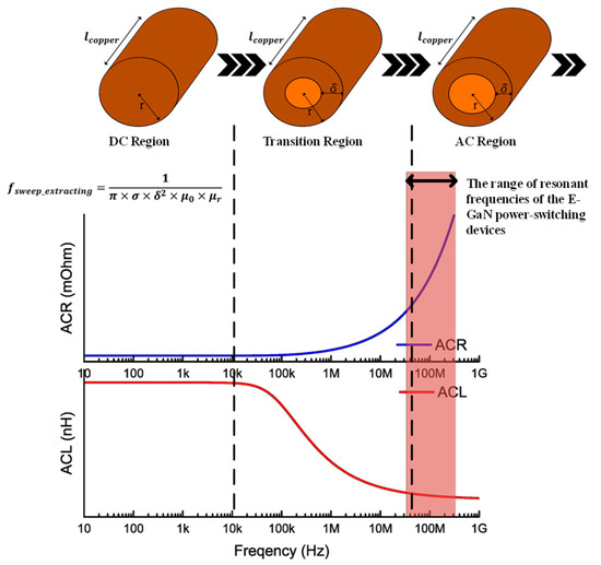
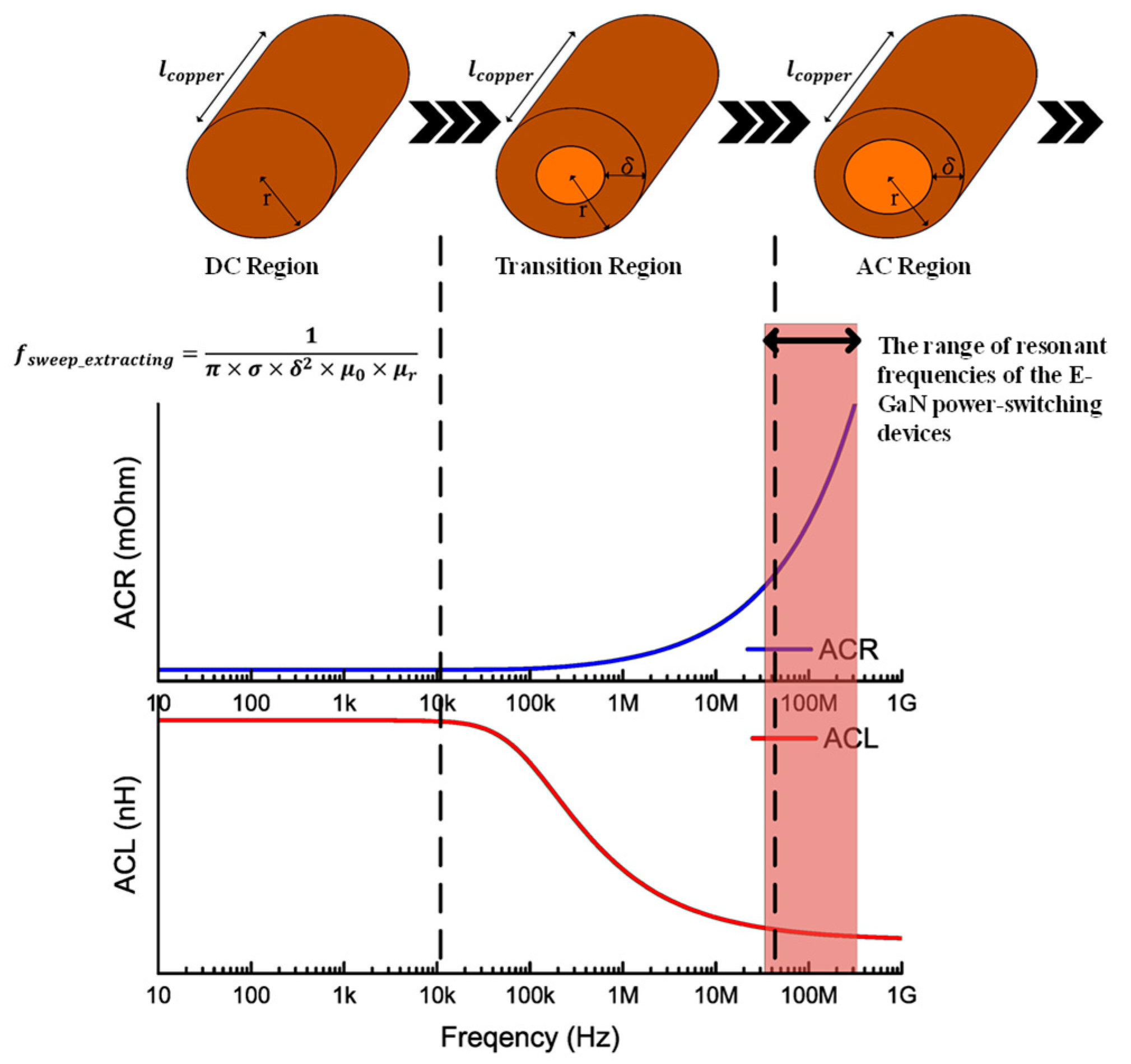
When extracting the parasitic inductance of the power loop using Ansys 2023 Q3D software, material properties and related parameters must be considered. The software calculates inductance and resistance based on the properties of copper and relevant formulas, considering the skin effect. As frequency increases, the inductance and parasitic resistance characteristics of copper change, as shown in Figure 7. Therefore, a frequency sweep is required to capture data, particularly within the resonance range of GaN power-switching devices, to ensure an accurate evaluation of the impact of parasitic effects on circuit performance.
Figure 7.
The relationship between the ACR and ACL and the skin depth.
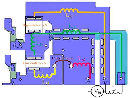
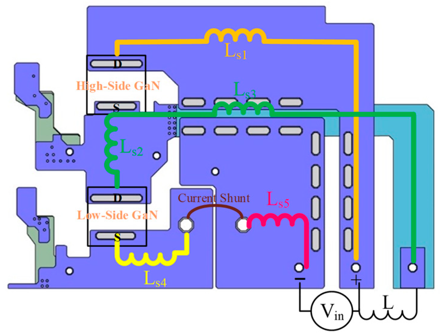
Step 1: In examining the parasitic inductance model, the initial step involves verifying the current paths within the main power circuit of the DPT circuit. Throughout this procedure, emphasis is placed on the low-side GaN switch circuit. In the preceding section, a comprehensive analysis of the DPT circuit’s operation was provided. By contrast, this section is dedicated to extracting parasitic inductance. To accomplish this objective, an approach from the PCB perspective is necessary, with a focus on the power loop, as illustrated in Figure 8. The inductance of each trace segment can be determined using these paths. In summary, a clear understanding of the current loop in the low-side GaN of the DPT circuit can be attained through this analytical process. Moreover, pertinent information about the power loop from the PCB viewpoint can be grasped. A detailed understanding of the inductance characteristics of each trace segment is gained by extracting the main loop paths, contributing to a more profound understanding of the entire parasitic inductance model.
Figure 8.
PCB of DPT circuit.
Step 2: When utilizing FEA tools to calculate parasitic inductance values, initially configuring the excitation source and the frequency scanning method is crucial. A voltage source is used to set the excitation source, and the excitation conditions are defined in a simulated manner. Simultaneously, selecting the frequency scanning method is highly important. Frequency scanning, typically ranging from low to high frequencies, is preferred to acquire parasitic inductance values across different frequency ranges. This approach facilitates the examination of performance variations in parasitic inductance at various operating frequencies. The stepping and range of the scanning should be predefined to ensure comprehensive coverage of the required frequency range.
Step 3: The obtained parasitic inductance is incorporated upon establishing the DPT mathematical model. This step determines the impact of parasitic inductance in the analysis, thereby creating a more comprehensive mathematical model. This analysis seeks to quantify the parasitic inductance present in DPT circuits, providing a clear understanding of potential uncertainties during the operation of switch components. The application of these analysis results in real-world scenarios allows for an accurate understanding and assessment of the performance of switch components. The ultimate objective is to mitigate uncertainties, enabling a precise analysis of the operation of switch components. This systematic approach contributes to enhancing the accuracy of DPT circuit analysis while ensuring accurate prediction and management of the potential impact of parasitic inductance on system performance in practical applications. Therefore, through this process, a thorough analysis of power switch components can be conducted.
3.2. Placement of Metal Vias
Understanding wire inductance begins with the fundamental formula for PCB trace inductance, from which further research and developments have evolved, as shown in Formula (16):
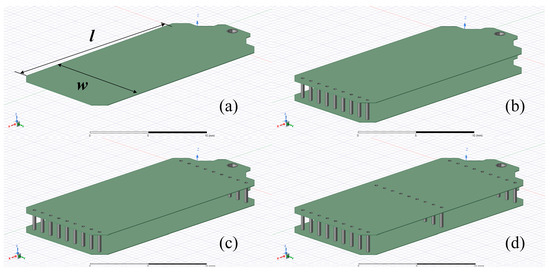
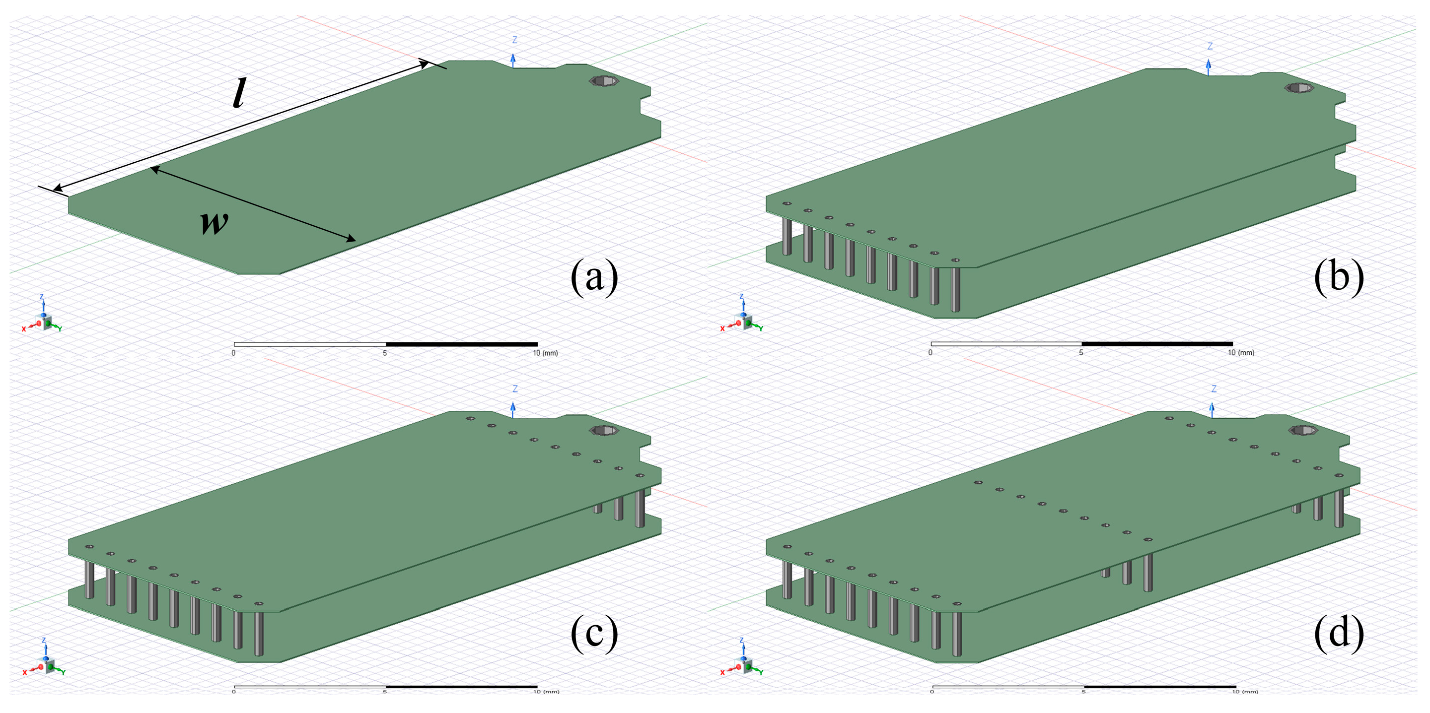
where μ0 is the vacuum permeability, h is the distance between two PCB traces, w is the width of the PCB trace, and l is the length of the PCB trace. This section addresses the method used to place the metal vias to minimize parasitic inductance and to prevent oscillations caused by the switch devices’ parasitic capacitance and parasitic inductance on the power loop, which can occur at frequencies in the megahertz range. The PCB traces are simplified to straight lines based on fundamental principles. Four different metal via layouts are used to define the inputs and outputs consistently. Scan parameters are initially set to default values, with a trace width of 10 mm and a trace length of 18 mm, as listed in Table 1. Sequential drilling is employed to observe the impact of metal vias on changes in parasitic inductance, as shown in Table 1.
Table 1.
Model parameters for frequency sweep.
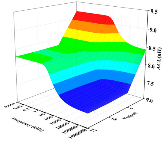
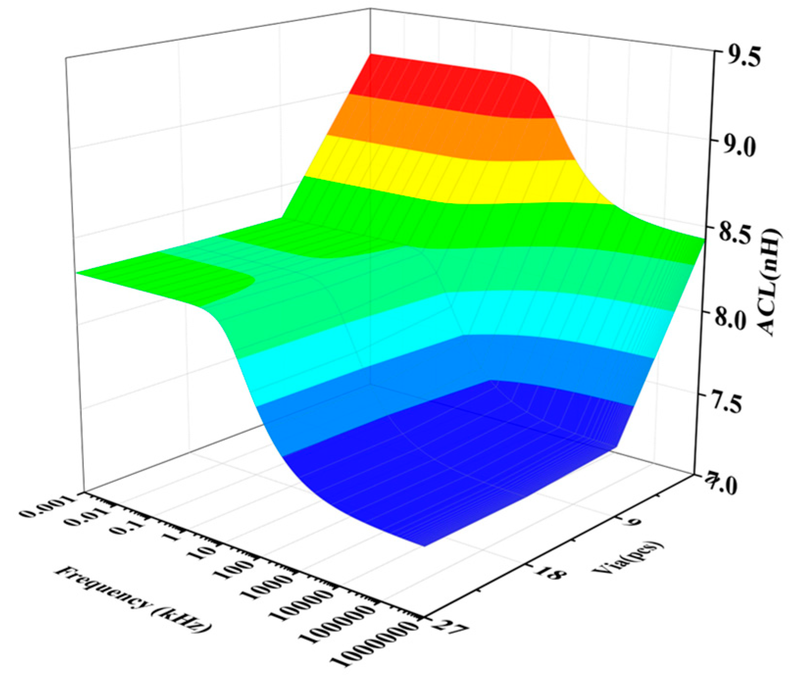
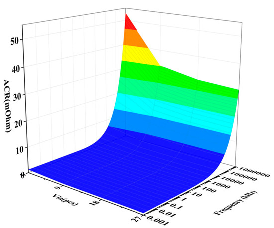
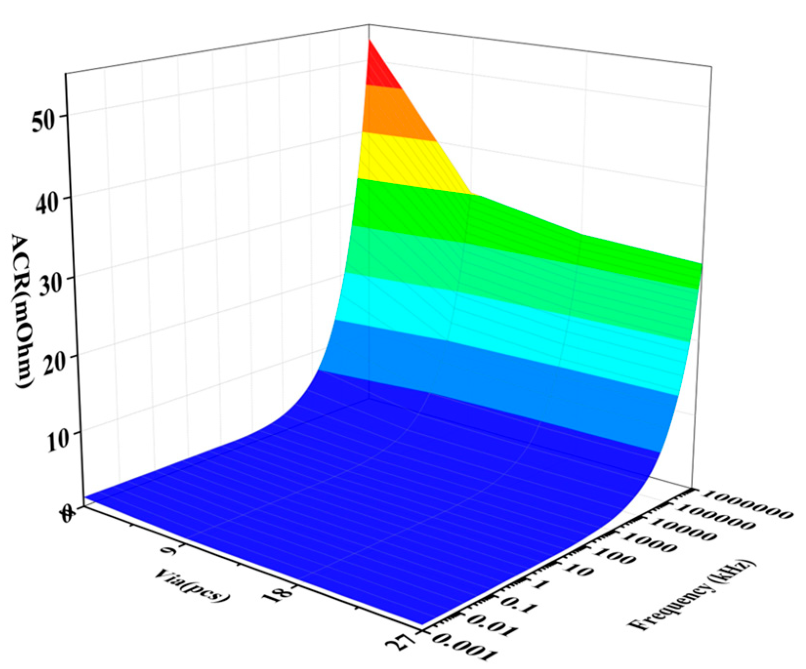
Figure 9a displays a flat trace without any vias. In Figure 9b, a single row of metal vias is shown, totaling nine vias. Figure 9c depicts the placement of two rows of metal vias, resulting in 18 vias. Figure 9d shows three rows of metal vias dispersed from input to output, with a total of 27 vias. Using FEA software, parasitic inductance and resistance values were extracted from the PCB copper at different frequencies to observe the effects of these four distinct via placements. The ACL (Figure 10) and ACR (Figure 11) curves, plotted based on frequency variations, demonstrate that increasing the number of vias helps reduce parasitic inductance and resistance.
Figure 9.
Placement of metal vias for a two-layer trace. (a) A flat trace without any vias; (b) A single row of metal vias, nine vias; (c) Two rows of metal vias, eighteen vias; (d) Three rows of metal vias, twenty-seven vias.
Figure 10.
Metal vias vs. ACL vs. frequency.
Figure 11.
Metal vias vs. ACR vs. frequency.
As the number of vias increases, the total volume of copper also increases. Therefore, the total amount of these four different types of copper is normalized. For example, in Figure 7, lcopper remains constant, and skin depth is also a fixed value, determined based on the extracted frequency. The radius of the circle, r, varies with the total volume, with the extent of this variation depending on the total volume size. As a result, an increase in vias leads to a larger copper area. Based on the fundamental resistance formula, the calculated resistance decreases, while the fundamental inductance formula indicates a corresponding decrease in inductance.
Proper via placement is crucial, and Table 2 provides the ACL and ACR values under various frequency conditions; dispersing the vias effectively reduces parasitic inductance.
Table 2.
The model parameters based on the frequency sweep placement.
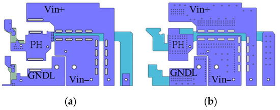
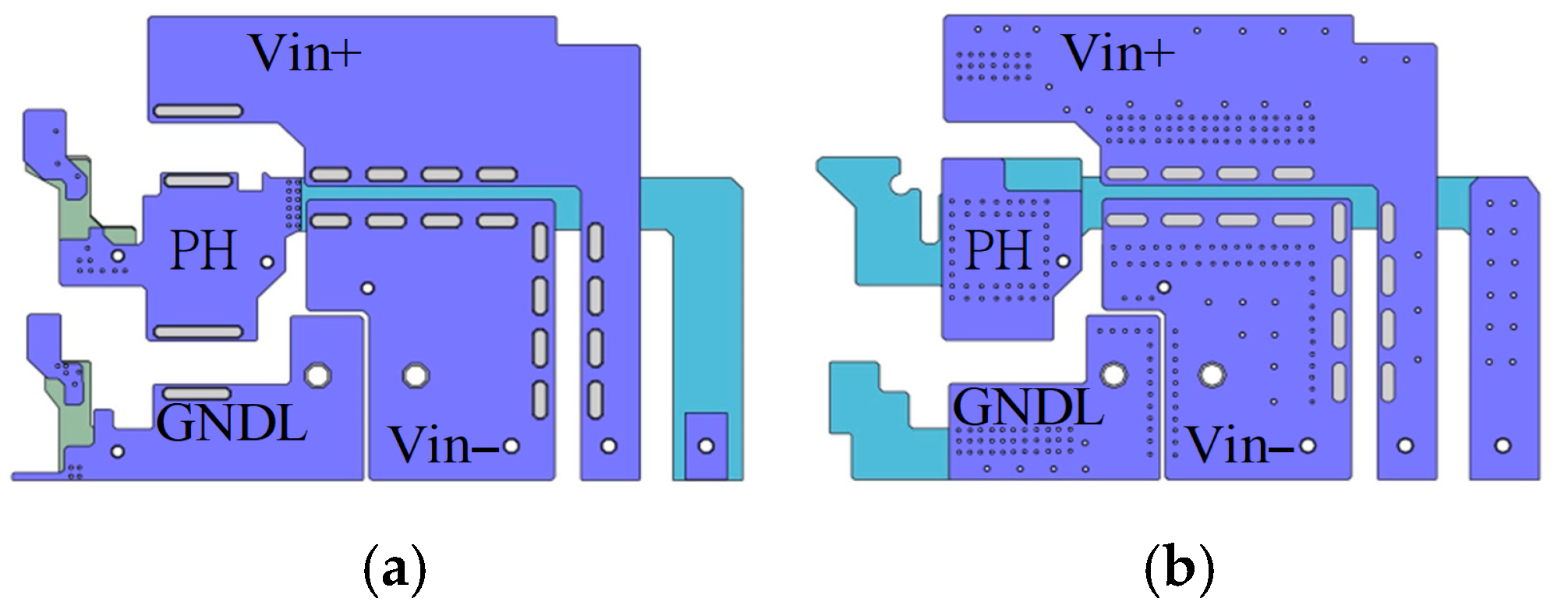
The effect of parasitic inductance should be enhanced to address potential compromises in layout integrity stemming from mechanical issues, albeit within a trade-off context. The solution elucidated in the preceding section, aimed at mitigating inductance, is extrapolated to tangible circuit applications. This strategy involves implementing a dispersed approach to further attenuate parasitic inductance within the PCB trace. After FEA simulations, the acquired inductance data can be assimilated into an established mathematical model for validation, thereby affirming the reduction in inductance. Consequently, this reduction curtails oscillations linked to the junction capacitance of switch devices. Prior to discussing the results, the four nomenclatural definitions pertaining to the copper plane, namely, Vin+, Vin−, PH, and GNDL, are explained. Following this elucidation, an examination of the specified inductance values outlined in each section is presented, as shown in Table 3. Figure 12a illustrates the design, relying exclusively on copper plane connections, abstaining from the implementation of a dispersed layout methodology. By contrast, Figure 12b introduces a modification by adopting a dispersed layout approach, incorporating the interconnection of discrete PCB layers through the integration of metal vias. The figure clearly shows the implications of the dispersed layout approach, revealing a clear diminishing trend in parasitic inductance values as the frequency progressively increases.
Table 3.
Extracting separate parasitic inductance values (a) without and (b) with dispersed vias.
Figure 12.
(a) Without and (b) with dispersed vias.
The test waveform results estimated from the two boards show minimal differences compared with the finite element analysis results, approximately ±2 nH, as shown in Table 4.
Table 4.
Extracting combined parasitic inductance values (a) without and (b) with dispersed vias and a comparison of test values.
4. Experimental Validation
4.1. Parasitic Inductance Lt and the Coss of E-GaN
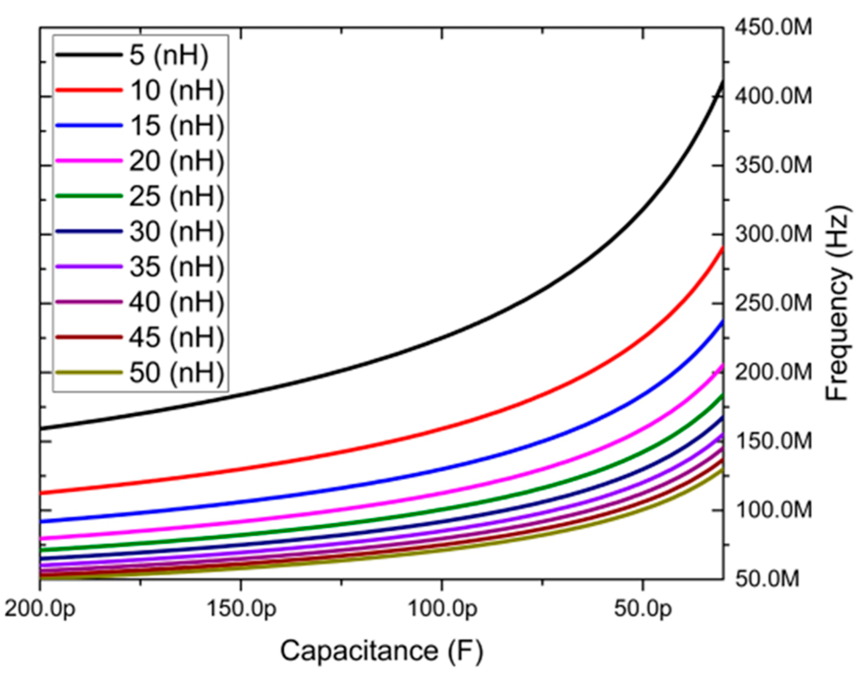
The inductor Lt on the PCB, alongside the parasitic capacitance Coss of the switching component, forms a resonant circuit. By applying the formula for a basic RLC series resonant circuit, as shown in Formula (17), the relationship between these components can be analyzed. The parasitic capacitance Coss of a commercially available E-GaN power-switching device typically ranges from 50 to 150 pF. Similarly, the parasitic inductance Lt on the PCB generally falls between 5 and 50 nH for standard PCB traces.
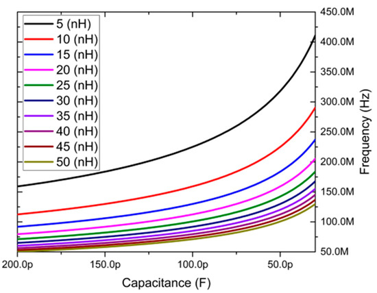
To illustrate the impact of these parameters, the curves plotted in Figure 13 are visible, which show the variation in resonance frequency. This frequency ranges approximately from 50 to 450 MHz. Based on these findings, a frequency sweep method can be employed in finite element analysis (FEA) software to extract the parasitic inductance values from the PCB.
Figure 13.
The resonance frequency vs. Coss.
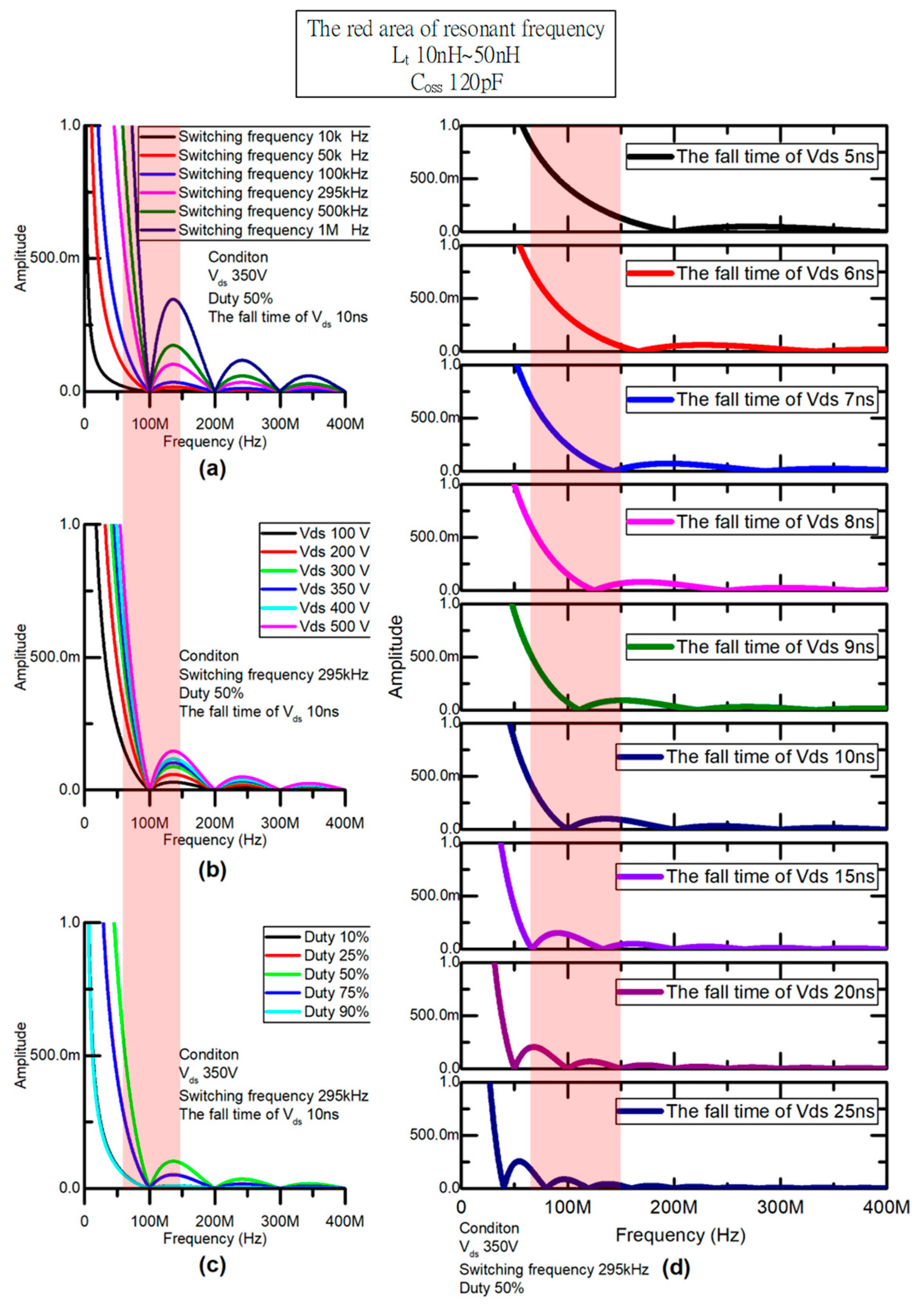
When the power-switching devices toggles, the drain-to-source voltage (Vds) of the switching device exhibits a square wave pattern, making it crucial to monitor this input voltage condition. To analyze its frequency-domain characteristics, fast Fourier transform (FFT) analysis can be applied, treating the Vds waveform as a fundamental square wave, as shown in Figure 14. This approach enables a more in-depth investigation of the resonant effects generated by the fundamental Vds square wave on the PCB’s parasitic inductance (Lt) and the parasitic output capacitance (Coss) of the switching component.
Figure 14.
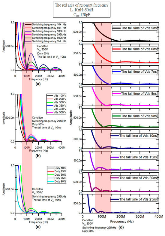
The FFT analysis of Vds of the approximate square wave. (a) Increasing switching frequency; (b) Increasing input voltage; (c) Adjusting the duty cycle; (d) Increasing the fall time of the Vds voltage.
As the switching frequency increases, the influence of the basic square wave of Vds on the resonance amplitude becomes more pronounced, as shown in Figure 14a. Similarly, an increase in the input voltage results in a higher amplitude, as shown in Figure 14b. Furthermore, when adjusting the duty cycle, the maximum amplitude usually occurs at a 50% duty cycle, as shown in Figure 14c. Changes in switching frequency, duty cycle, or input voltage primarily affect the amplitude, which corresponds to the changes along the Y-axis of the curve.
Another important factor to consider is the fall time and slope of the Vds voltage. Different fall rates result in variations in the spectral changes, and the slope of the fall is influenced by the switching current and the Coss parameter. As illustrated in Figure 14d, in the basic square wave approximation, an increase in the fall rate of the Vds voltage (i.e., when the Vds voltage drops faster) causes the frequency range of the first wave to shift upward.
Examining the impact of the Vds on the FFT curve reveals important insights regarding the Lt and Coss curves. A decrease in resonance frequency, as indicated by Lt and Coss, generally suggests an increase in parasitic inductance. This increase leads to higher resonance amplitude, which subsequently affects the oscillation of the switching current. Additionally, it results in a greater overlap between Vds and Ids, ultimately increasing switching losses. For instance, when the commercial switch devices, identified as GS66516T, operate under a 350 V condition with a Coss of approximately 120 pF, the parasitic inductance can vary from 10 to 50 nH at a 50% duty cycle. This can be assessed through the square wave FFT curve, which shows resonance frequency points within the range of 65 to 150 MHz, as highlighted in the red area in Figure 14.
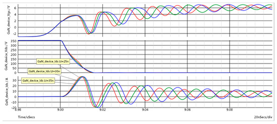
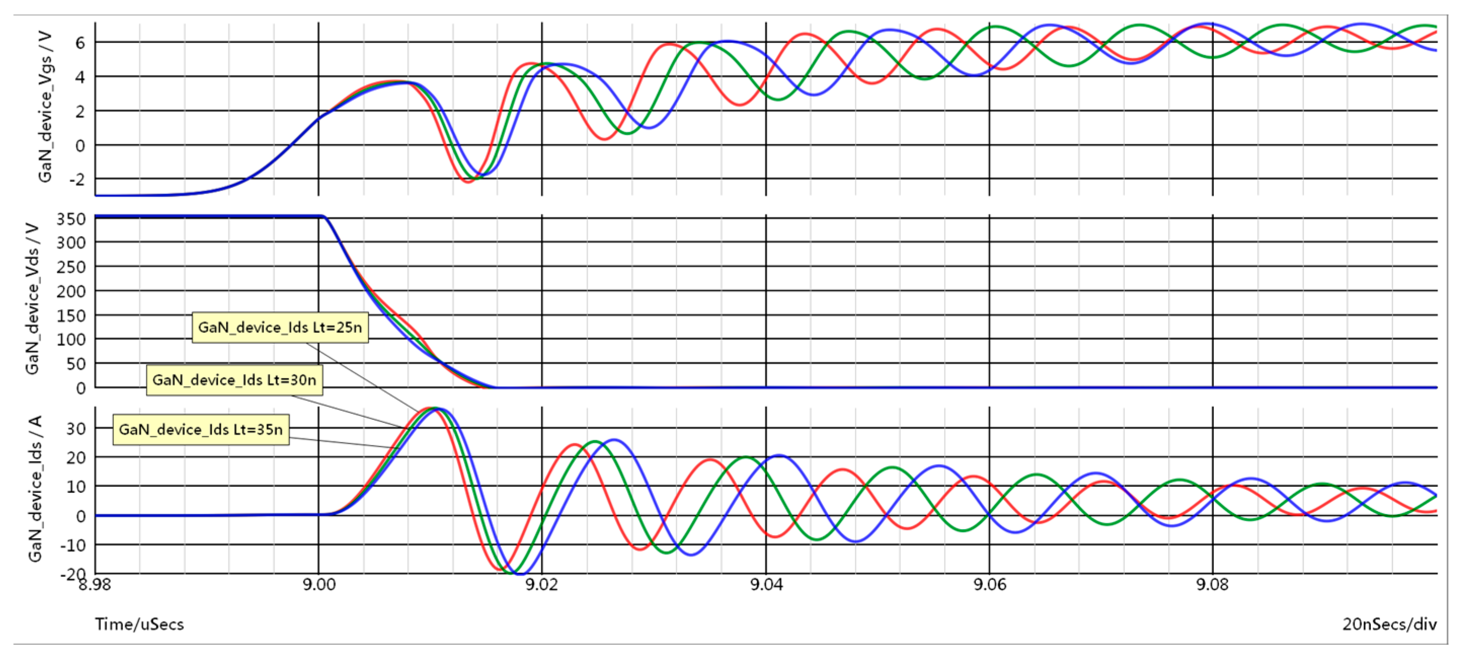
To verify this phenomenon, simulation software was used to observe the time-domain waveforms, as shown in Figure 15. A lower frequency results in greater energy overlap between Vds and Ids at the switching point, leading to an increase in switching losses. Additionally, Figure 16 presents the actual circuit test results, confirming the simulated trends and demonstrating the impact of different parasitic inductance values.
Figure 15.
Simulation with different Lt values.
Figure 16.
Comparison of Lt in a real circuit and the turn-on energy of Vgs. CH1: Vgs; CH2: Vds; CH3: Ids; Math: Energy, CH2*CH3.
From the test results in Figure 16, an analysis of the Ids current at the switching point allows for an estimation of the parasitic inductance, and the inductance value can be calculated using Formula (17). As parasitic inductance increases, the Vds slope falls slower, contributing to higher switching losses. Therefore, minimizing parasitic inductance during the PCB layout process is crucial for improving switching efficiency, making it a key aspect of PCB design.
This section examines the characteristics by approximating the voltage on the switch as a square wave and performing an FFT frequency domain analysis. It also introduces the working principle of the DPT circuit and the interaction between parasitic capacitance on the switch and parasitic inductance on the PCB. These analyses provide a deeper understanding of their roles and relationships in switching operations.
4.2. Circuit Validation and Test Configuration
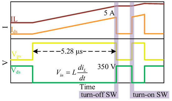
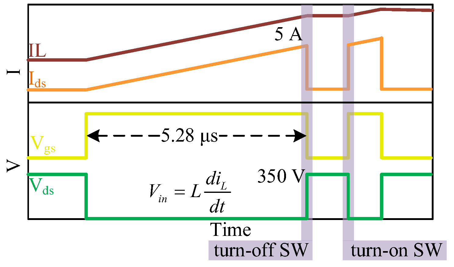
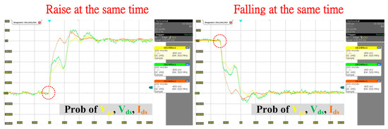
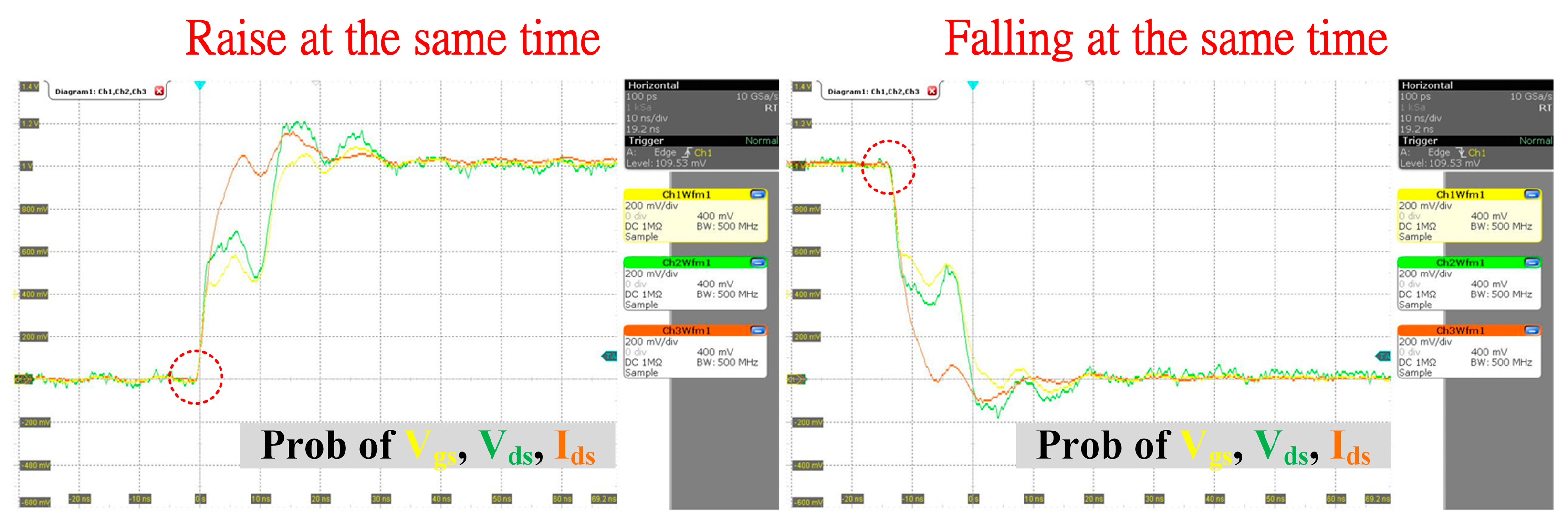
The DPT circuit utilizes a modular design to ensure testing under the same conditions. The board includes half-bridge transistors, decoupling capacitors, and gate drivers. Here, we briefly introduce the testing parameters of the DPT circuit: time is adjusted based on fixed inductance, current, and voltage, following values specified in Figure 17. For example, under testing conditions of 350 V, 5 A, and 370 µH, the required time is 5.28 µs. During the design process, the charging inductor’s timing is adjusted with reference to the actual parameter. In the entire system, the digital signal processor is responsible for providing gate signals through optical fibers. Simultaneously, precise voltage measurements are made using passive (high-bandwidth) probes. The switching current on the measurement path is measured using a low-inductance current shunt through a BNC coaxial cable. During testing, the primary step is to calibrate the probes. This strategy is crucial because GaN components have extremely fast switching speeds, reaching levels in the nanosecond range. Any delay in voltage and current waveforms could potentially affect accuracy. Therefore, calibrating the probes becomes crucial, as shown in Figure 18, where each probe is adjusted to the same starting and ending points. When selecting an oscilloscope, a higher resolution is recommended to ensure that the probes have sufficient bandwidth for accurate measurements, as shown in Table 5.
Figure 17.
Illustration of DPT.
Figure 18.
Calibration of each probe. All probes move in sync, as highlighted by the red circles.
Table 5.
List of test parameters.
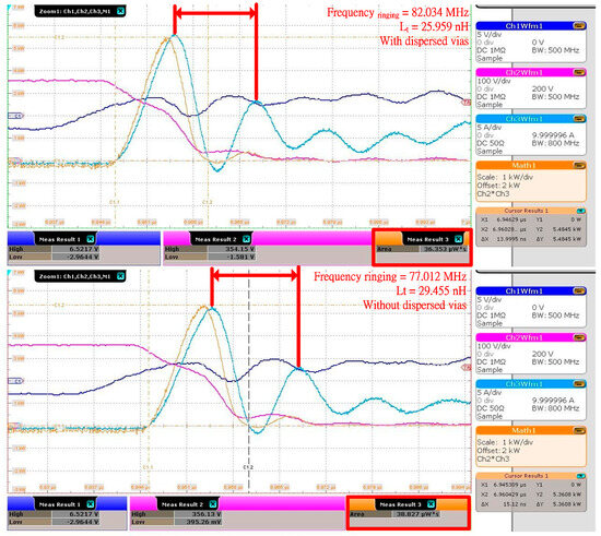
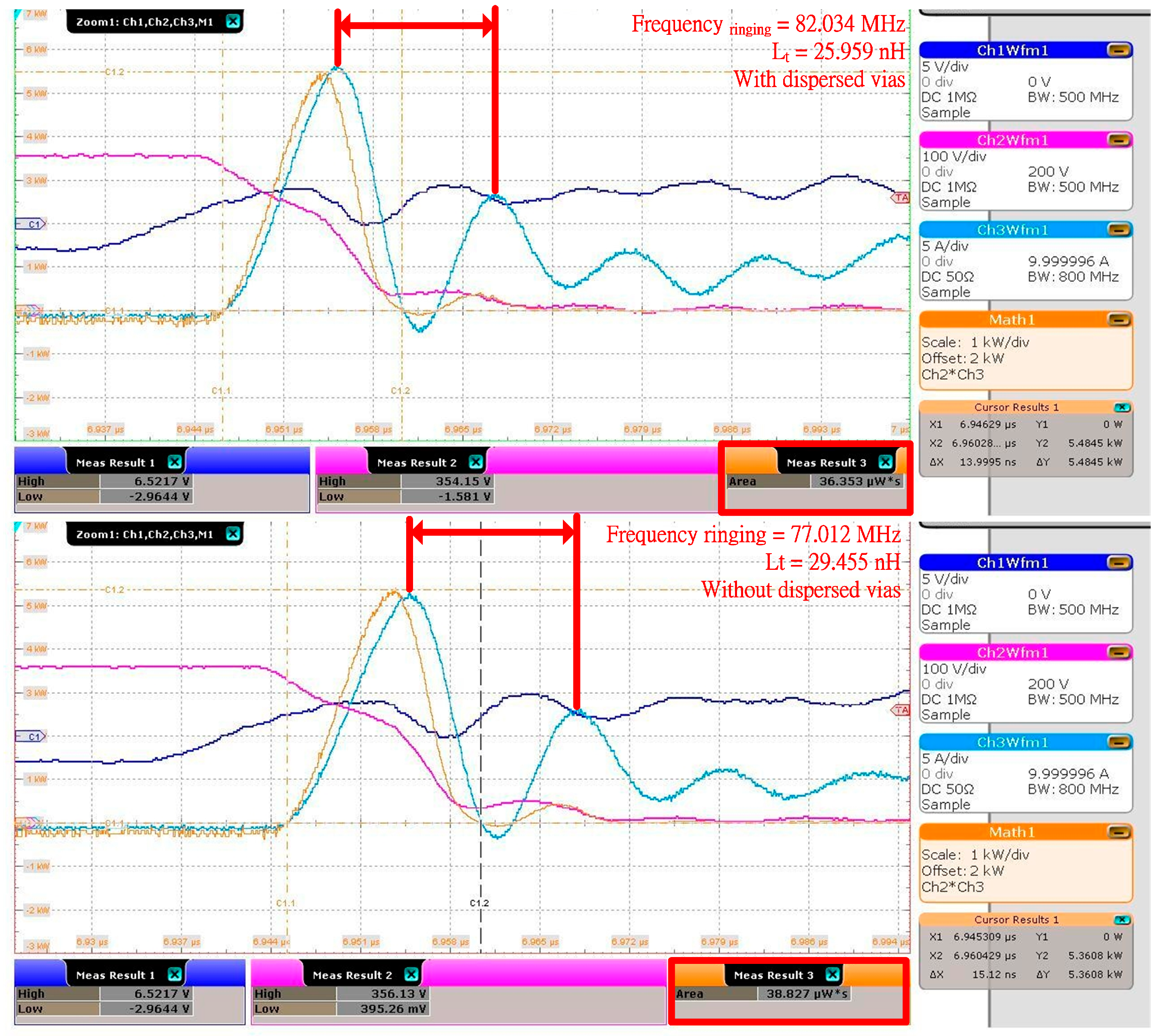
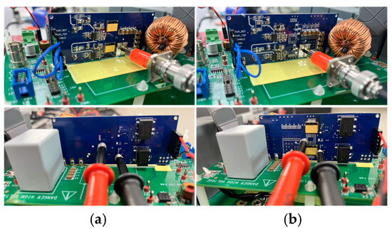
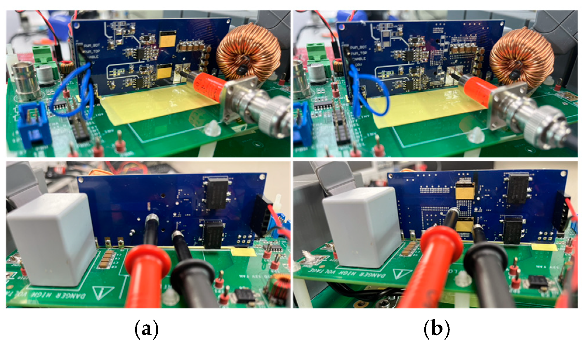
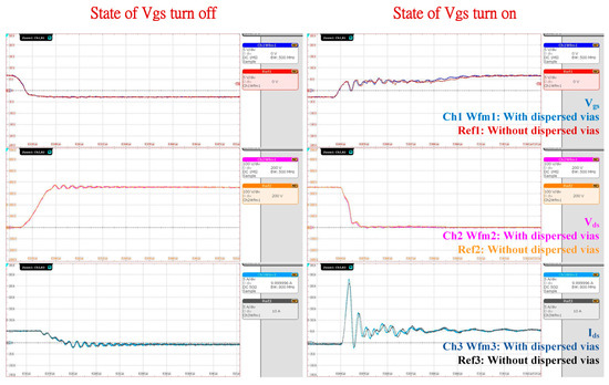
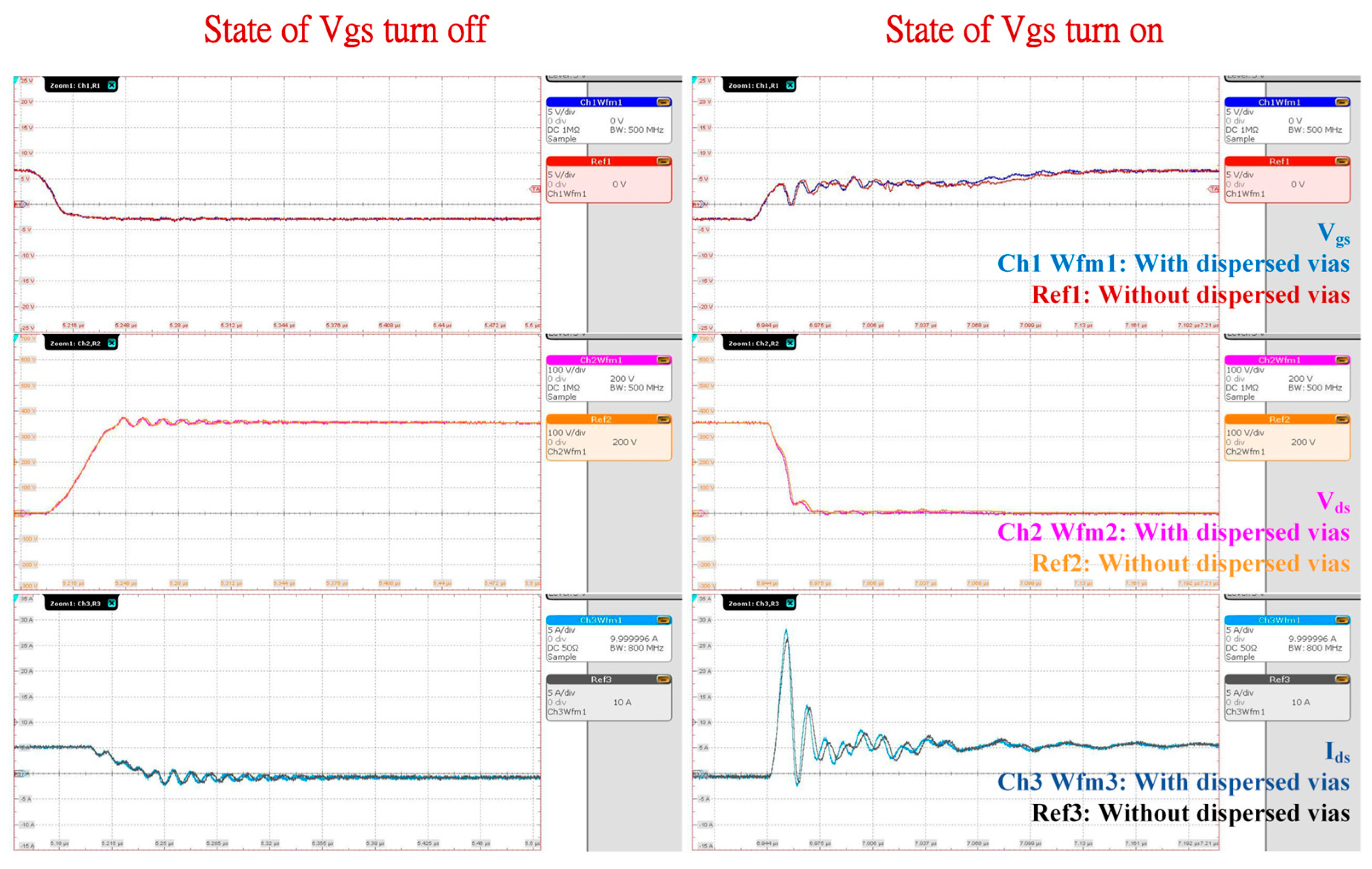
A comparison of tests between two boards is provided in Figure 19. As shown in Figure 20, the absence of dispersed vias leads to more severe ringing. The Vgs comparison reveals that without dispersed vias, the turn-on process exhibits a noticeable delay, which correlates with the increased ACL and ACR discussed in the previous section. It was previously noted that as inductance increases, the current ringing time also extends, which increases the crossover area.
Figure 19.
Boards (a) without and (b) with dispersed vias.
Figure 20.
Comparison of Vgs, Vds, and Ids without and with dispersed vias.
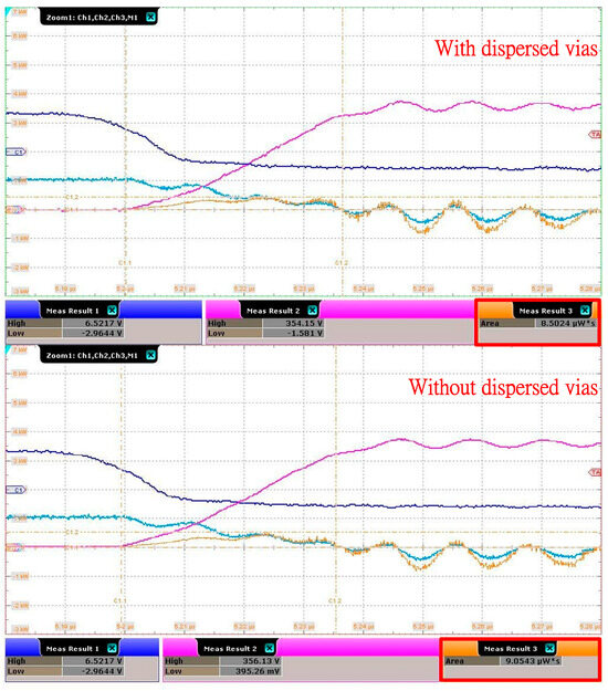
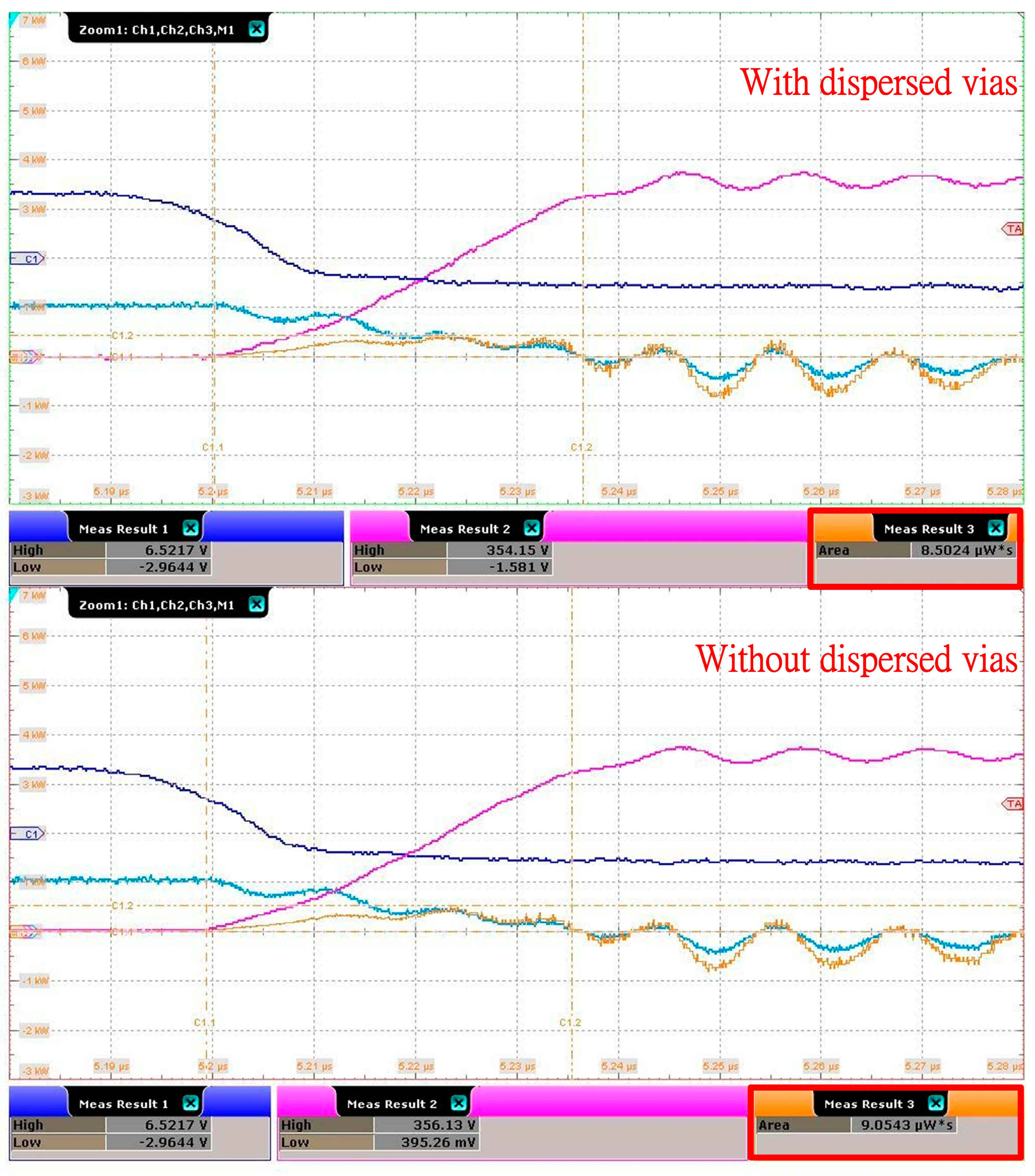
Figure 16 shows the turn-on Vgs, and Figure 21 shows the turn-off Vgs. The test results for turn-on switching with dispersed vias show an energy consumption of 36.353 µW·s, whereas without dispersed vias, it is 38.827 µW·s, resulting in a difference of 2.47 µW·s. The test results for turn-off switching with dispersed vias show an energy consumption of 8.5024 µW·s, whereas without dispersed vias, it is 9.0543 µW·s, resulting in a difference of 0.5519 µW·s, as shown in Table 6.
Figure 21.
Comparison of the turn-off energy of Vgs. CH1: Vgs; CH2: Vds; CH3: Ids.
Table 6.
Comparison of parasitic inductance and measured switching energy losses.
5. Conclusions
This study provides an in-depth analysis of E-GaN switching components, establishing a thorough understanding of the DPT basic circuit platform through detailed circuit analysis. Building on this foundation, the investigation reveals oscillation issues, emphasizing the impact of parasitic inductance in the PCB power loop on switching losses. FEA and measurement results indicate that parasitic inductance varied by approximately ±2 nH during testing. By optimizing the distributed metal layout, parasitic inductance was effectively reduced by about 5 nH, leading to an approximate reduction of 2 µW·s in energy consumption for practical circuit applications. Additionally, this approach enhances the accuracy of switching device evaluations. Through a systematic analysis of the key parameters, this study not only highlights the effects of various circuit components but also introduces precise data estimation methods, providing valuable insights for improving the circuit performance and optimizing the power loop design.
Author Contributions
Conceptualization, X.-R.C.; Methodology, X.-R.C.; Software, Y.-Y.C.; Validation, Y.-X.Y.; Formal analysis, X.-R.C.; Investigation, X.-R.C.; Resources, Y.-C.L.; Data curation, X.-R.C.; Writing—original draft, X.-R.C.; Writing—review & editing, H.-J.C.; Supervision, H.-J.C.; Project administration, X.-R.C., H.-J.C. and Y.-C.L. All authors have read and agreed to the published version of the manuscript.
Funding
This research received no external funding.
Data Availability Statement
The original contributions presented in this study are included in the article. Further inquiries can be directed to the corresponding author.
Conflicts of Interest
The authors declare no conflicts of interest.
References
- Khan, M.A.; Simin, G.; Pytel, S.G.; Monti, A.; Santi, E.; Hudgins, J.L. New Developments in Gallium Nitride and the Impact on Power Electronics. In Proceedings of the 2005 IEEE 36th Power Electronics Specialists Conference, Dresden, Germany, 16 June 2005; pp. 15–26. [Google Scholar] [CrossRef] [Scilit]
- Kaminski, N. State of the art and the future of wide band-gap devices. In Proceedings of the 2009 13th European Conference on Power Electronics and Applications, Barcelona, Spain, 8–10 September 2009; pp. 1–9. [Google Scholar]
- Amano, H.; Baines, Y.; Beam, E.; Borga, M.; Bouchet, T.; Chalker, P.R.; Charles, M.; Chen, K.J.; Chowdhury, N.; Chu, R.; et al. The 2018 GaN power electronics roadmap. J. Phys. D Appl. Phys. 2018, 51, 163001. [Google Scholar] [CrossRef] [Scilit]
- Kozak, J.P.; Zhang, R.; Porter, M.; Song, Q.; Liu, J.; Wang, B.; Wang, R.; Saito, W.; Zhang, Y. Stability; Reliability, and Robustness of GaN Power Devices: A Review. IEEE Trans. Power Electron. 2023, 38, 8442–8471. [Google Scholar] [CrossRef] [Scilit]
- Liu, Z.; Huang, X.; Lee, F.C.; Li, Q. Package Parasitic Inductance Extraction and Simulation Model Development for the High-Voltage Cascode GaN HEMT. IEEE Trans. Power Electron. 2014, 29, 1977–1985. [Google Scholar] [CrossRef] [Scilit]
- Gareau, J.; Hou, R.; Emadi, A. Review of Loss Distribution, Analysis, and Measurement Techniques for GaN HEMTs. IEEE Trans. Power Electron. 2020, 35, 7405–7418. [Google Scholar] [CrossRef] [Scilit]
- Chen, J.; Du, X.; Luo, Q.; Zhang, X.; Sun, P.; Zhou, L. A Review of Switching Oscillations of Wide Bandgap Semiconductor Devices. IEEE Trans. Power Electron. 2020, 35, 13182–13199. [Google Scholar] [CrossRef] [Scilit]
- Xin, Y.; Chen, W.; Sun, R.; Shi, Y.; Liu, C.; Xia, Y.; Wang, F.; Li, M.; Li, J.; Zhou, Q.; et al. Analytical Switching Loss Model for GaN-Based Control Switch and Synchronous Rectifier in Low-Voltage Buck Converters. IEEE J. Emerg. Sel. Top. Power Electron. 2019, 7, 1485–1495. [Google Scholar] [CrossRef] [Scilit]
- Zhang, Y.; Xu, W.; Xie, Y.; Liu, T.; Wu, Z.; Chen, C.; Kang, Y.; Peng, H. Analysis of Dead-Time Energy Loss in GaN-Based TCM Converters with an Improved GaN HEMT Model. IEEE Trans. Power Electron. 2023, 38, 1806–1818. [Google Scholar] [CrossRef] [Scilit]
- Emon, A.I.; Mustafeezul, H.; Mirza, A.B.; Kaplun, J.; Vala, S.S.; Luo, F. A Review of High-Speed GaN Power Modules: State of the Art, Challenges, and Solutions. IEEE J. Emerg. Sel. Top. Power Electron. 2023, 11, 2707–2729. [Google Scholar] [CrossRef] [Scilit]
- Sun, B.; Jørgensen, K.L.; Zhang, Z.; Andersen, M.A.E. Research of Power Loop Layout and Parasitic Inductance in GaN Transistor Implementation. IEEE Trans. Ind. Appl. 2021, 57, 1677–1687. [Google Scholar] [CrossRef] [Scilit]
- Reusch, D.; Strydom, J. Understanding the Effect of PCB Layout on Circuit Performance in a High-Frequency Gallium-Nitride-Based Point of Load Converter. IEEE Trans. Power Electron. 2014, 29, 2008–2015. [Google Scholar] [CrossRef] [Scilit]
- Gurpinar, E.; Iannuzzo, F.; Yang, Y.; Castellazzi, A.; Blaabjerg, F. Design of Low-Inductance Switching Power Cell for GaN HEMT Based Inverter. IEEE Trans. Ind. Appl. 2018, 54, 1592–1601. [Google Scholar] [CrossRef] [Scilit]
- Kozak, J.P.; Barchowsky, A.; Hontz, M.R.; Koganti, N.B.; Stanchina, W.E.; Reed, G.F.; Mao, Z.-H.; Khanna, R. An Analytical Model for Predicting Turn-ON Overshoot in Normally-OFF GaN HEMTs. IEEE J. Emerg. Sel. Top. Power Electron. 2020, 8, 99–110. [Google Scholar] [CrossRef] [Scilit]
- Huang, X.; Li, Q.; Liu, Z.; Lee, F.C. Analytical Loss Model of High Voltage GaN HEMT in Cascode Configuration. IEEE Trans. Power Electron. 2014, 29, 2208–2219. [Google Scholar] [CrossRef] [Scilit]
- Xia, Y.K.; Li, X.Y. Calculation and Experiment of Stray Inductance of PCB Double-Pulse Test Circuit Based on Three-Dimensional Simulation. IEEE Access 2022, 10, 58769–58776. [Google Scholar] [CrossRef] [Scilit]
- Xu, Y.Q.J.; Chen, D.; Lu, J.; Hou, R.; Di Maso, P. An Experimental Comparison of GaN EHEMTs Versus SiC MOSFETs over Different Operating Temperatures; GaN Systems Inc.: Ottawa, ON, Canada, 2018. [Google Scholar]
- Jones, E.A. Review and Characterization of Gallium Nitride Power Devices. Master’s Thesis, University of Tennessee, Knoxville, TN, USA, 2016. Available online: https://trace.tennessee.edu/utk_gradthes/4048 (accessed on 25 October 2023).
- Kohlhepp, B.; Faber, S.; Kübrich, D.; Dürbaum, T. PCB Layout Parasitics Extraction of a GaN Half-Bridge: Simulation and Experimental Validation. In Proceedings of the 2023 25th European Conference on Power Electronics and Applications (EPE’23 ECCE Europe), Aalborg, Denmark, 4–8 September 2023; pp. 1–9. [Google Scholar] [CrossRef] [Scilit]
- Ahmed, M.R.; Todd, R.; Forsyth, A.J. Predicting SiC MOSFET Behavior Under Hard-Switching, Soft-Switching, and False Turn-On Conditions. IEEE Trans. Ind. Electron. 2017, 64, 9001–9011. [Google Scholar] [CrossRef] [Scilit]

Disclaimer/Publisher’s Note: The statements, opinions and data contained in all publications are solely those of the individual author(s) and contributor(s) and not of MDPI and/or the editor(s). MDPI and/or the editor(s) disclaim responsibility for any injury to people or property resulting from any ideas, methods, instructions or products referred to in the content. |
© 2026 by the authors. Licensee MDPI, Basel, Switzerland. This article is an open access article distributed under the terms and conditions of the Creative Commons Attribution (CC BY) license.