


Abstract
This study presents a high-efficiency T-type three-level inverter for interior permanent magnet synchronous motor (IPMSM) drive applications, featuring a comprehensive performance comparison with a conventional two-level inverter. To address the high switching losses and noticeable harmonic distortion typically associated with conventional two-level configurations, the T-type architecture is developed and evaluated. First, PLECS simulations are conducted to verify the proposed dual-loop control architecture, which integrates field-oriented control (FOC), space-vector pulse-width modulation (SVPWM), and a neutral-point voltage balancing mechanism. Subsequently, a 2.2 kW experimental platform is constructed using silicon carbide (SiC) wide-bandgap (WBG) semiconductor devices. To characterize the dynamic switching behavior of the adopted SiC MOSFETs, a dedicated double-pulse test (DPT) platform is developed to evaluate their switching losses and determine appropriate gate-drive parameters. In addition, the digital control firmware is implemented on a digital signal processor (DSP) platform. The dual-loop control algorithms, SVPWM strategy, and two-layer protection framework are implemented as real-time executable routines, enabling close integration of the control software and hardware platform. Finally, motor drive experiments at switching frequencies of 20 kHz and 40 kHz are performed to validate the proposed system. The experimental results demonstrate that the developed architecture significantly reduces phase-current total harmonic distortion (THD) and improves overall energy conversion efficiency compared with a conventional two-level inverter, confirming its potential for high-efficiency next-generation electric vehicle applications.
1. Introduction
As global climate change intensifies and environmental awareness continues to increase, stringent regulations on internal combustion engine vehicles have made EVs [1,2] an inevitable global trend. Consequently, the efficiency of power inverters and electric motors has become increasingly critical. Optimizing energy conversion efficiency extends vehicle range, reduces the size of the cooling system, and enhances overall reliability under demanding operating conditions. Thus, developing advanced inverter topologies and high-efficiency motors [3] has become an important research focus in both academia and industry.
AC drive systems [4] offer several advantages over DC drive systems, including lightweight construction, efficient regenerative braking, robustness, reliability, and near-maintenance-free operation, all of which are essential for EV applications. Among AC motors, compared with induction motors (IM), the rotor of a permanent-magnet synchronous motor (PMSM) utilizes permanent magnets. Consequently, the stator current does not need to supply magnetizing current, resulting in a higher power factor and efficiency at the same output. Furthermore, PMSMs [5,6,7,8] dominate the EV motor sector due to their strong overload capacity and high efficiency during acceleration and deceleration.
Power semiconductors directly affect the efficiency of power converters. As traditional silicon (Si) devices approach their physical limits, wide-bandgap materials such as SiC and gallium nitride (GaN) are gaining prominence. Compared with conventional Si devices, WBG devices [9,10] possess higher critical breakdown electric fields and lower on-resistance, enabling operation at higher voltages, frequencies, and junction temperatures while reducing switching losses.
Recent comparative evaluations of Si, SiC, and GaN devices in inverters have demonstrated that wide-bandgap materials can further elevate system efficiency [11]. Among these devices, SiC has achieved broader adoption than GaN in EV traction inverters and high-voltage converters, primarily due to its superior thermal conductivity, which supports efficient thermal management in compact, high-power modules [12]. Although GaN offers high switching speeds, its low gate-threshold voltage and narrow allowable gate-voltage range make it susceptible to oscillations caused by parasitic inductance under high dv/dt conditions, increasing the risk of false triggering. Consequently, SiC MOSFETs remain preferred for high-reliability applications due to their mature technology and robust thermal performance.
Dynamic characterization [13,14] is essential for power electronics design, providing insights into the switching behavior, efficiency, and thermal performance of semiconductor devices under actual operating conditions. The DPT circuit architecture [15], comprising the power module, DC capacitors, gate driver, and load inductor, is widely used to evaluate the dynamic performance of power modules.
Three-level inverters, such as neutral-point-clamped (NPC) and T-type topologies, offer reduced switching losses, lower semiconductor voltage stress, higher power density, and improved harmonic performance compared with traditional two-level voltage-source inverters (VSIs) [16,17,18]. The T-type inverter is particularly suitable for low- to medium-voltage applications, including EV drivetrains below 800 V [19]. It retains the low conduction losses of conventional two-level VSIs because its asymmetrical voltage distribution allows the main switches to withstand the full DC-link voltage, while the neutral-point switches withstand only half, enabling lower-voltage devices with lower on-resistance. In addition, fewer components than the NPC topology simplify control and system design. By balancing switching and conduction losses, the T-type inverter [20,21,22] provides high-efficiency power conversion with reliable performance in automotive applications.
Despite these advancements, many existing studies evaluating the T-type topology lack direct experimental comparisons with conventional two-level configurations. To explicitly address these literature gaps, this study develops a high-efficiency SiC-based T-type three-level IPMSM drive system to demonstrate its advantages over the conventional two-level baseline. The main contributions of this work include utilizing a dedicated DPT platform to optimize gate-drive parameters, implementing a simplified carrier-based SVPWM strategy integrated with dual-layer protection on a DSP platform, and conducting an experimental comparative evaluation. Ultimately, this study systematically visualizes the benefits of the T-type architecture, highlighting its superior energy conversion efficiency and significant reduction in phase-current THD compared to the traditional two-level inverter under practical operating conditions.
This article is a revised and expanded version of a paper (Paper No. K260193) [23] entitled “Development and Performance Analysis of a High-Efficiency Interior Permanent Magnet Synchronous Motor Drive System Based on a T-type Three-Level Inverter”, which was presented at the 9th International Conference on Knowledge Innovation and Invention 2026 (ICKII 2026), Sendai, Japan, 14–16 August 2026.
This study is organized into seven sections. A brief outline of each section is presented as follows: Section 1 introduces the research motivation, background, and literature survey, followed by the organization of the paper. Section 2 provides an overview of the fundamental characteristics of permanent magnet synchronous motors and the operating principles of the T-type three-level inverter. Section 3 describes the system simulation constructed in the PLECS environment. It details the FOC strategy integrated with SVPWM and verifies the effectiveness of the neutral-point voltage balancing control for the T-type architecture. Section 4 presents the dynamic characterization of power modules using the double-pulse test. Section 5 focuses on the real-time firmware architecture developed on the DSP platform. It details the progressive firmware expansion from basic motor control to specific T-type logic, including the allocation of computational tasks to the control law accelerator and the implementation of a dual-layer system protection framework. Section 6 provides comprehensive experimental results and performance comparisons between the conventional two-level reference and the proposed T-type inverter. It evaluates the conversion efficiency and phase-current THD under different switching frequencies. Section 7 summarizes the major contributions and conclusions of this research and proposes several potential directions for future investigation.
2. Configuration and Control of the Proposed T-Type IPMSM Drive
This section introduces the power-stage configuration and control architecture of the proposed T-type three-level inverter-fed IPMSM drive system. The carrier-based SVPWM strategy, switching logic, and neutral-point voltage balancing mechanism are described before their effectiveness is evaluated through PLECS simulations.
2.1. System Configuration
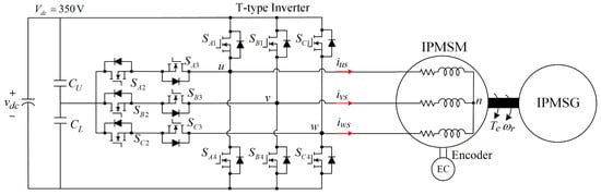
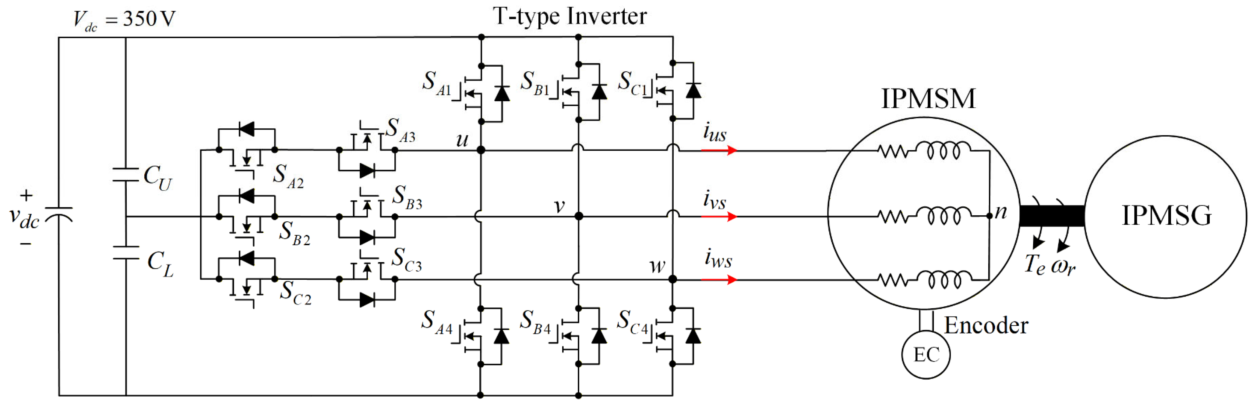
The system configuration of the proposed IPMSM drive system is shown in Figure 1. The system consists of a DC power source, a split DC-link formed by two series-connected capacitors, a T-type three-level inverter, an IPMSM. The DC link voltage is set to 350 V, and the upper and lower DC-link capacitors and are used to establish a neutral point for three-level voltage operation. The T-type inverter contains three identical phase legs. The three-phase inverter outputs are directly connected to the stator windings of the IPMSM, and the phase currents and are supplied to the motor. An encoder is employed to provide rotor position and speed information for feedback control in the DSP. In addition, an IPMSG was mechanically coupled to the motor shaft, and an electrical load was connected to the generator terminals to serve as the load torque.
Figure 1.
System configuration of the IPMSM drive system.
2.2. Carrier-Based Three-Level SVPWM
Although three-level SVPWM offers superior performance, its implementation requires region identification and dwell-time calculation, resulting in considerable computational burden. Therefore, a simplified strategy based on two-level zero-sequence injection is adopted to convert the three-phase sinusoidal reference signals into saddle-shaped modulation waves equivalent to SVPWM:
where denotes the corresponding system phase, and represents the original sinusoidal voltage reference of that phase. By algebraically incorporating the offset voltage, the DC-link voltage utilization is improved without requiring complex geometric calculations. To ensure the modified signals are correctly mapped onto the switching states of the T-type inverter, a polarity-based voltage-level assignment logic is adopted. This logic is established according to the physical arrangement of switches and defined in Figure 1. Furthermore, to prevent device damage, three fundamental forbidden states are strictly avoided: (1) simultaneous conduction of and , (2) and , and (3) and . According to the polarity of the modulation wave , the switching operations are restricted to the corresponding voltage subintervals, and the commutation sequences are arranged to avoid these forbidden switching configurations.
During transitions between stable states, a protection sequence is applied in which any switch conflicting with the subsequent state is turned off before the next device is activated. This ensures that only safe intermediate configurations occur during the dead-time interval. The corresponding switching-state and gate-signal assignments are summarized in Table 1.
Table 1.
Switching state mapping and operational logic.
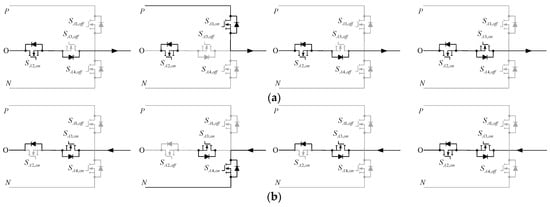
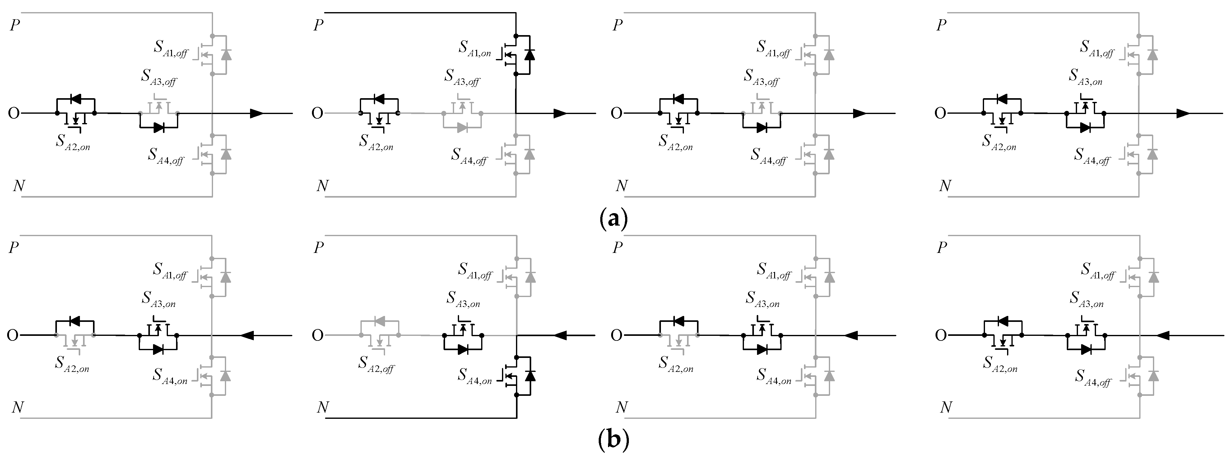
The switching sequence is determined by the phase-current polarity to prevent the forbidden states. As shown in Figure 2a, when the phase current is nonnegative, modulation is performed between States P and O. is turned off while remains on before is activated, whereas the reverse transition is completed by turning off before reactivating . For negative phase current, the phase leg switches between States O and N, as shown in Figure 2b. is turned off before is activated while remains on, and the reverse transition is performed by turning off before is reactivated. This current-dependent commutation sequence maintains a safe neutral-point current path, avoids the forbidden switch combinations, and enables a stable five-level line-to-line voltage output.
Figure 2.
Conduction paths of the T-type phase leg: (a) ; (b)
3. Simulation Verification
Based on the system configuration and carrier-based three-level SVPWM presented in Section 2, the proposed IPMSM drive system is modeled in PLECS for simulation verification. The proposed modulation strategy is integrated with the FOC-based dual-loop control and neutral-point voltage balancing mechanism to form the complete control architecture. To enable a control-oriented assessment, ideal switching devices and a stable DC bus are assumed in the simulation model. Ideal switching devices and a stable DC bus are assumed in the simulation model. Accordingly, non-ideal effects, including switching delays, parasitic components, and digital implementation delays, are neglected in this section. This assumption allows the analysis to focus clearly on the fundamental feasibility of the control architecture, modulation scheme and operational logic for the T-type inverter, establishing a verified baseline for the subsequent hardware implementation.
The main system parameters of the IPMSM drive, including the DC-link voltage, rated current, and switching frequency, are listed in Table 2. In addition, the electrical and mechanical parameters used in the simulations were selected according to the specifications of the actual motor and are summarized in Table 3.
Table 2.
Specifications of the IPMSM drive system.
Table 3.
Specifications and parameters of IPMSM.
3.1. Control Scheme of Simulation
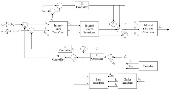
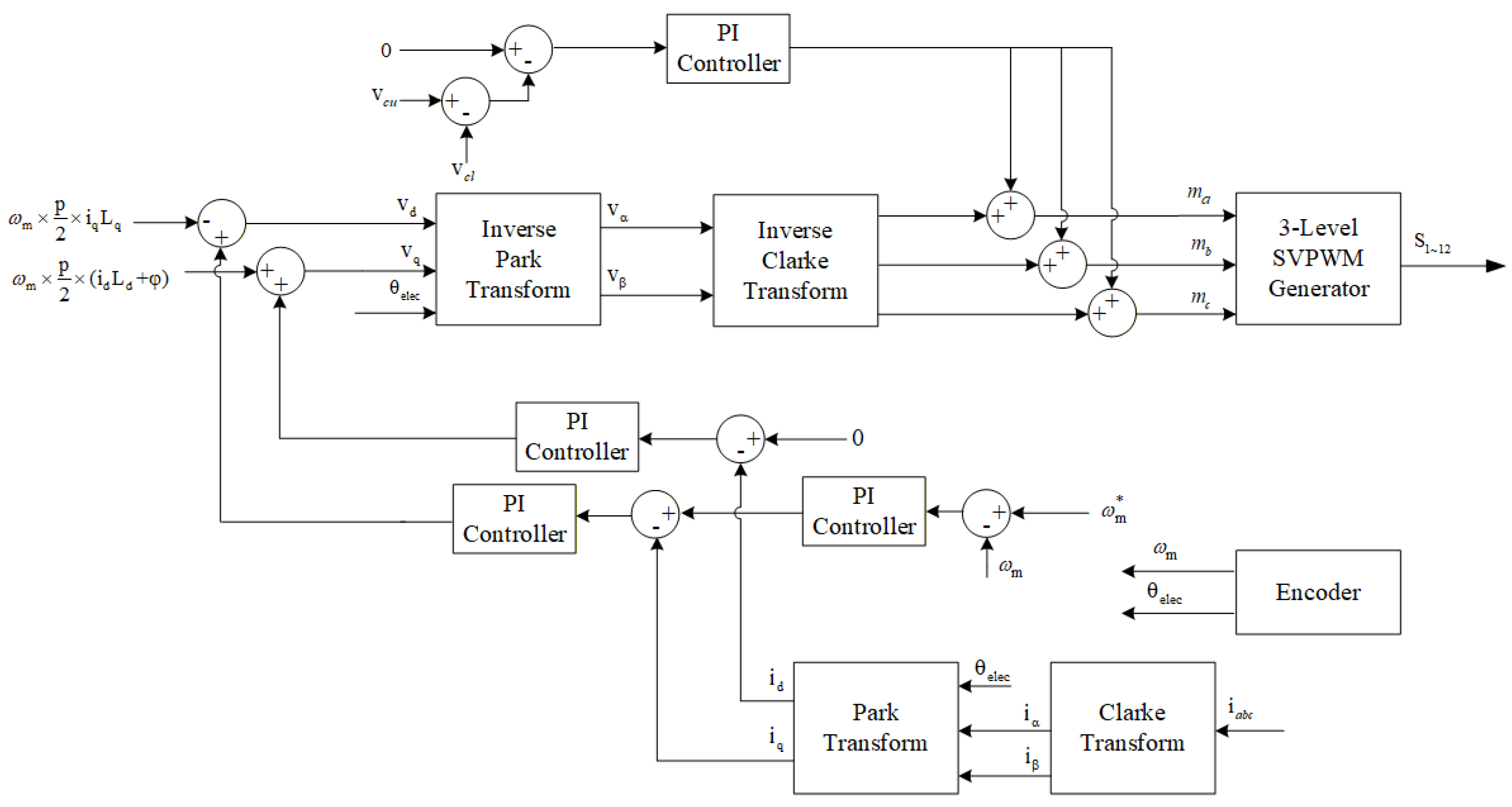
The integrated control architecture of the T-type inverter system is shown in Figure 3, in which FOC is employed to achieve high-performance motor-drive operation. The mechanical speed and rotor position are measured using the encoder and processed by the speed control loop to generate the torque-producing current reference. This reference is subsequently applied to the inner current control loop, where the decoupled d-axis and q-axis currents are controlled to obtain the required voltage commands. To ensure stable operation, a neutral-point voltage balancing compensator is incorporated to regulate the split-capacitor voltages and , while the total DC-link voltage is supplied by a regulated DC source. The resulting voltage commands are then converted into gate signals using the simplified zero-sequence-injection-based PWM scheme together with the current-polarity detection logic. This multi-loop control structure provides accurate motor-drive control while maintaining balanced split DC-link capacitor voltages. The PI controller parameters adopted in the PLECS model are listed in Table 4.
Figure 3.
The integrated control architecture for the T-type inverter system.
Table 4.
PI controller parameters in PLECS.
3.2. Simulation Results
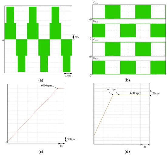
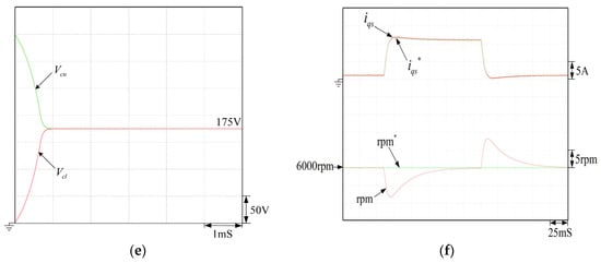
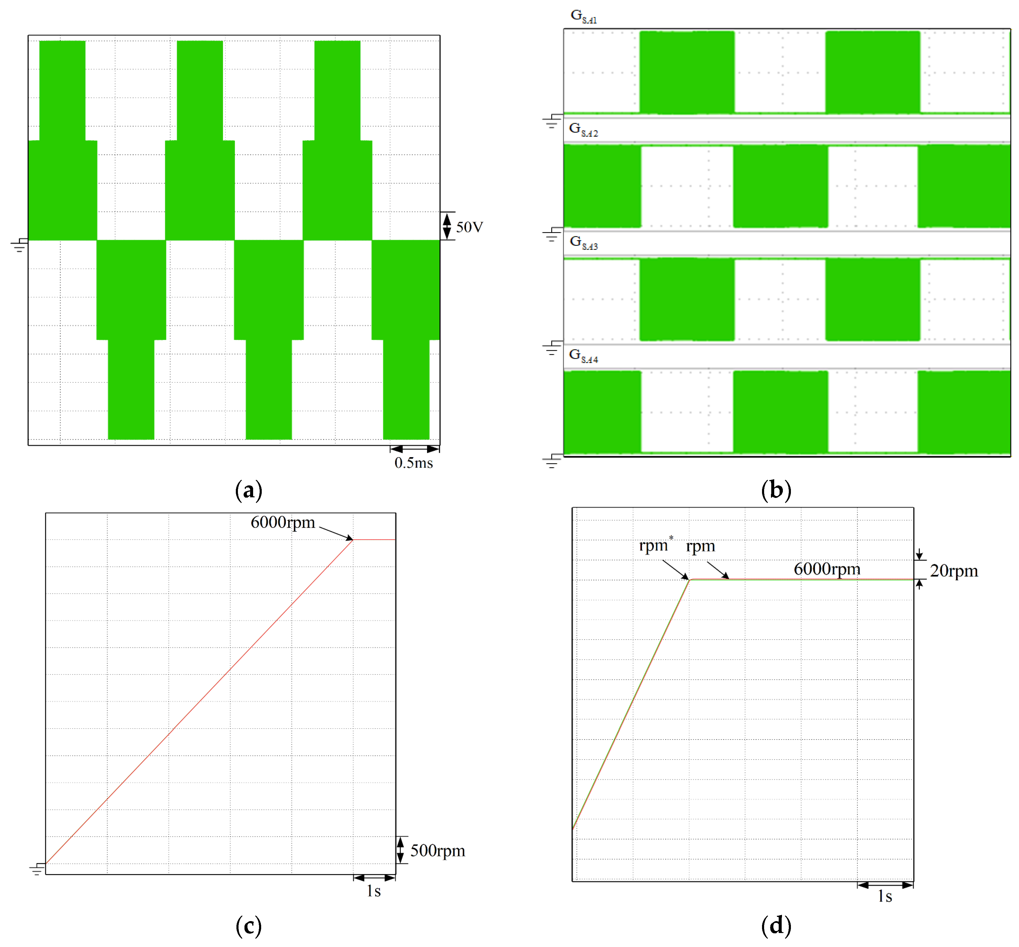
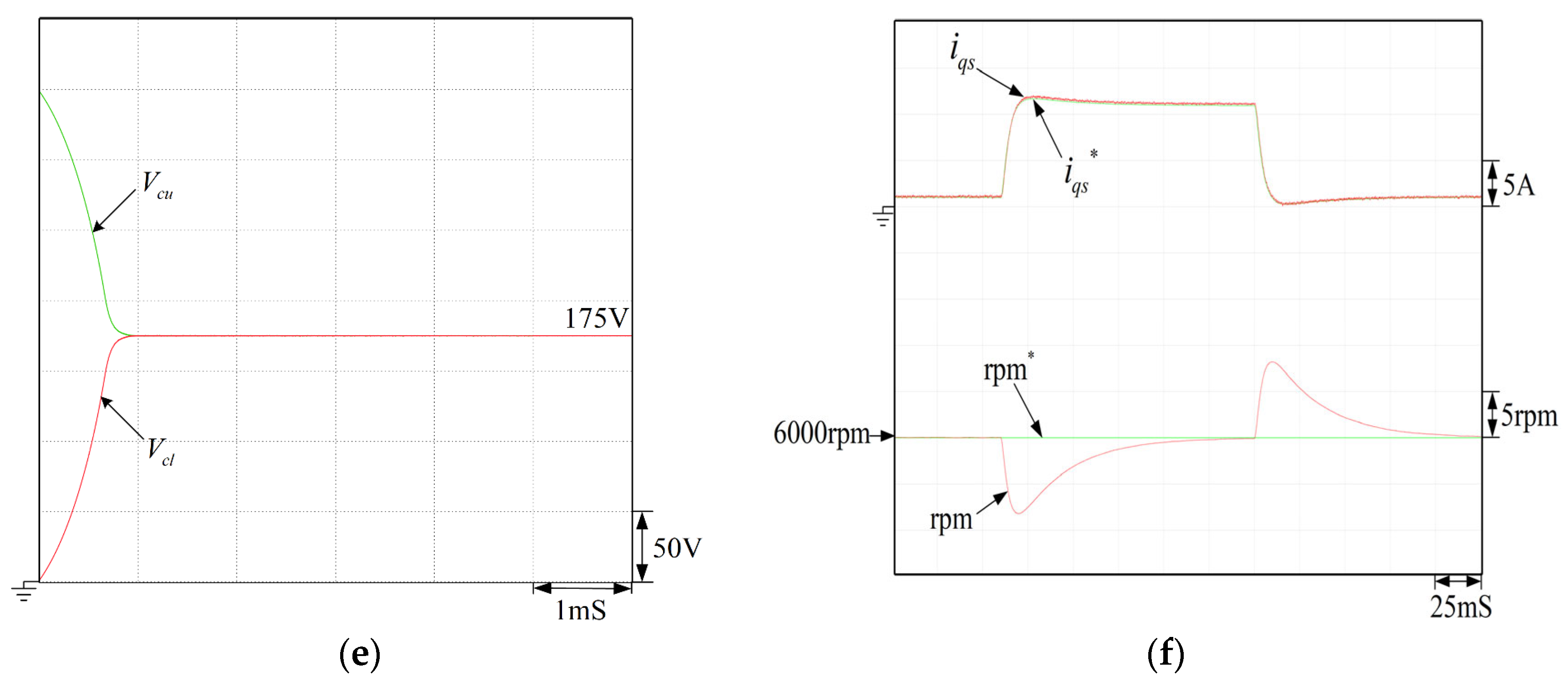
The simulation results of the proposed IPMSM drive system are shown in Figure 4. As illustrated in Figure 4a, the line-to-line voltage exhibits five distinct voltage levels, confirming the proper operation of the proposed carrier-based three-level SVPWM strategy. Figure 4b confirms that the switching sequences are executed based on the logic mentioned in Section 2. Figure 4c shows the motor speed response from standstill to a command of 6000 rpm. The motor follows the ramp reference smoothly without evident overshoot or instability. The enlarged steady-state waveform in Figure 4d further shows that the actual speed closely tracks the reference at 6000 rpm with only a small tracking error. In addition, the robustness of the neutral-point voltage balancing compensator is evaluated under severely unbalanced initial conditions, with and initially set to 349 V and 1 V, respectively. As shown in Figure 4e, both capacitor voltages are rapidly regulated toward the balanced operating point and converge to approximately 175 V, corresponding to half of the total DC-link voltage. Furthermore, Figure 4f demonstrates that the proposed control strategy along with well-tuned PI controllers can effectively achieve stable dynamic responses during sudden loading and de-loading conditions at the rated speed of 6000 rpm.
Figure 4.
Simulation results: (a) Line-to-line voltage of the proposed SVPWM strategy; (b) single-phase gate signal of the T-type inverter; (c) speed response from standstill to 6000 rpm; (d) zoomed-in steady-state speed tracking at 6000 rpm; (e) transient response of neutral-point voltage balancing control; and (f) and of the IPMSM drive under a step load change (10% loadfull load10% load, = 6000 rpm).
4. Double-Pulse Test and SiC Device Characterization
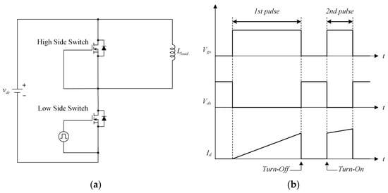
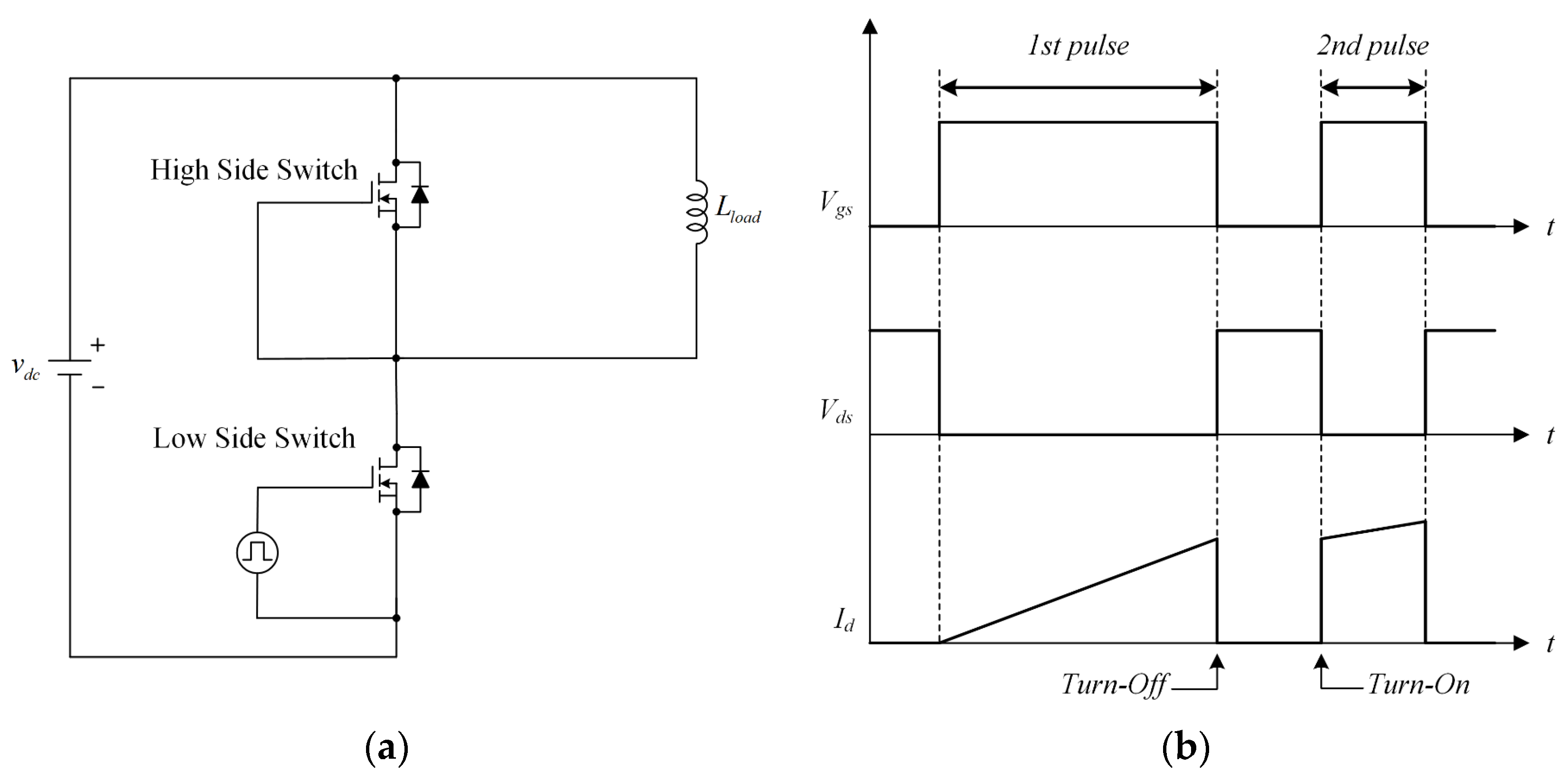
A double-pulse test (DPT) is employed to characterize the switching behavior of the SiC MOSFETs adopted in the T-type inverter under controlled voltage and current conditions.
As shown in Figure 5a, the DPT circuit consists of a regulated DC source, a half-bridge leg, and an inductive load. The first pulse establishes the required load current, and its falling edge is used to evaluate the turn-off characteristics. After a short freewheeling interval, the second pulse is applied to assess the turn-on behavior, as illustrated in Figure 5b.
Figure 5.
Principle of the double-pulse test: (a) Circuit schematic; (b) typical operating waveforms.
4.1. Experimental Setup and Test Conditions
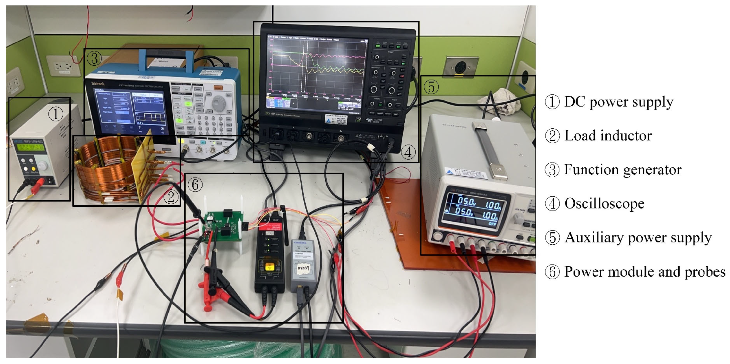
To accurately evaluate the dynamic switching characteristics of the selected SiC MOSFETs, this study developed a double-pulse test platform. The overall hardware configuration is shown in Figure 6. In terms of system architecture, the platform consists primarily of a digital signal generator responsible for outputting precise double-pulse timing, an auxiliary power supply providing a stable operating voltage for the isolated gate drive circuit, and a high-power DC power supply for establishing a high-voltage DC bus to simulate the actual operating voltage of the inverter. Together, these devices provide a complete dynamic test environment for the half-bridge power modules under test. The key specifications of this SiC MOSFET are summarized in Table 5, and the oscilloscope (Teledyne LeCroy, Chestnut Ridge, NY, USA), voltage probes (Cybertek, Shenzhen, China), and Rogowski current probe (Cybertek, Shenzhen, China) used in the DPT are listed in Table 6, together with their respective bandwidths.
Figure 6.
Photograph of the complete double-pulse test platform.
Table 5.
Key specifications of the selected SiC MOSFET.
Table 6.
Measurement equipment and bandwidths used in the DPT.
To evaluate the effects of DC-link voltage and switching slew rate on the switching losses and transient electrical stresses of the SiC MOSFET, two sets of DPT conditions are considered. First, the gate resistance is fixed, while the load current is varied from 3 A to 10 A under DC-link voltages of 200 V and 400 V, as summarized in Table 7. Subsequently, the DC-link voltage is fixed at 200 V, and different gate resistances are selected to obtain three target slew rates for both the turn-on and turn-off transitions over a load-current range of 0–10 A. The corresponding turn-on and turn-off test conditions are listed in Table 8 and Table 9, respectively.
Table 7.
Test conditions for evaluating the impact of DC-link voltage.
Table 8.
Test conditions for evaluating the impact of turn-on switching slew rate.
Table 9.
Test conditions for evaluating the impact of turn-off switching slew rate.
4.2. Experimental Results
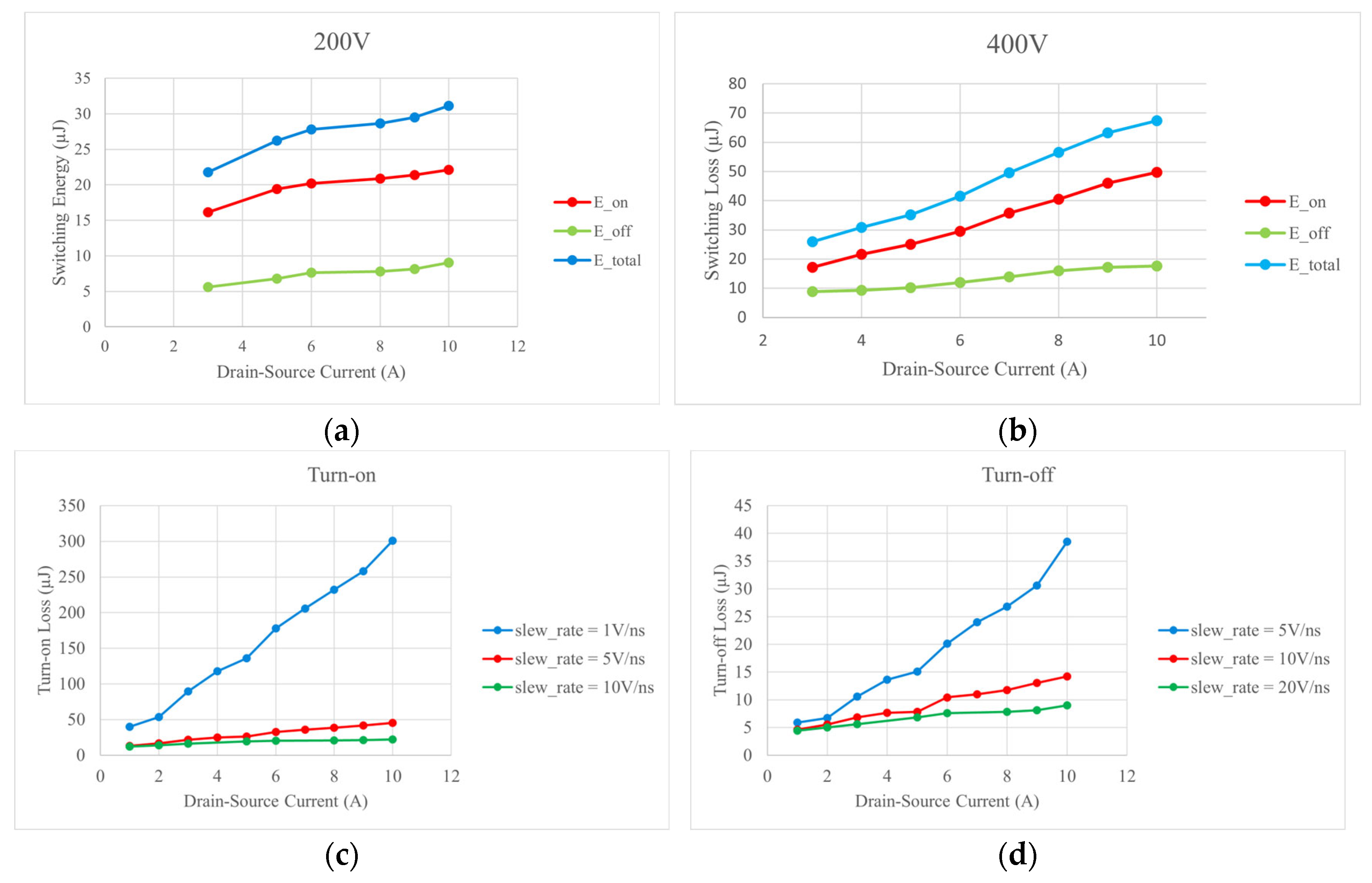
As shown in Figure 7a,b, the total switching energy increases with both the DC-link voltage and drain-source current. Compared with the 200 V condition, the switching energy measured at 400 V is consistently higher, and the difference becomes more pronounced as the current increases. Figure 7c,d further show that the switching energy decreases as the switching slew rate increases. At a drain-source current of 10 A, increasing the turn-on slew rate from 1 V/ns to 10 V/ns reduces the turn-on energy from approximately 300 μJ to below 50 μJ. Similarly, a turn-off slew rate of 20 V/ns yields lower turn-off energy than at 5 V/ns. Based on the measured loss trends and switching behavior, the gate resistance value of 10 Ω is selected for both and to achieve a suitable compromise between switching efficiency and operational stability.
Figure 7.
Measured switching-energy characteristics of the SiC MOSFET under different DC-link voltages and switching slew rates: (a) Switching energies at 200 V; (b) switching energies at 400 V; (c) turn-on energy under different turn-on slew rates; and (d) turn-off energy under different turn-off slew rates.
5. DSP Firmware Implementation
To accommodate the modular hardware platform, the control firmware is developed in a progressive manner. The baseline FOC and SVPWM routines are first implemented and experimentally verified using the two-level inverter configuration. Based on this verified framework, the firmware is subsequently extended to the T-type three-level inverter by incorporating the proposed carrier-based three-level SVPWM, neutral-point voltage balancing, two-layer protection. This staged implementation enables both inverter configurations to operate on the same DSP platform and provides a consistent basis for the subsequent experimental comparison.
5.1. Firmware Architecture
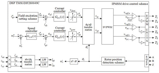
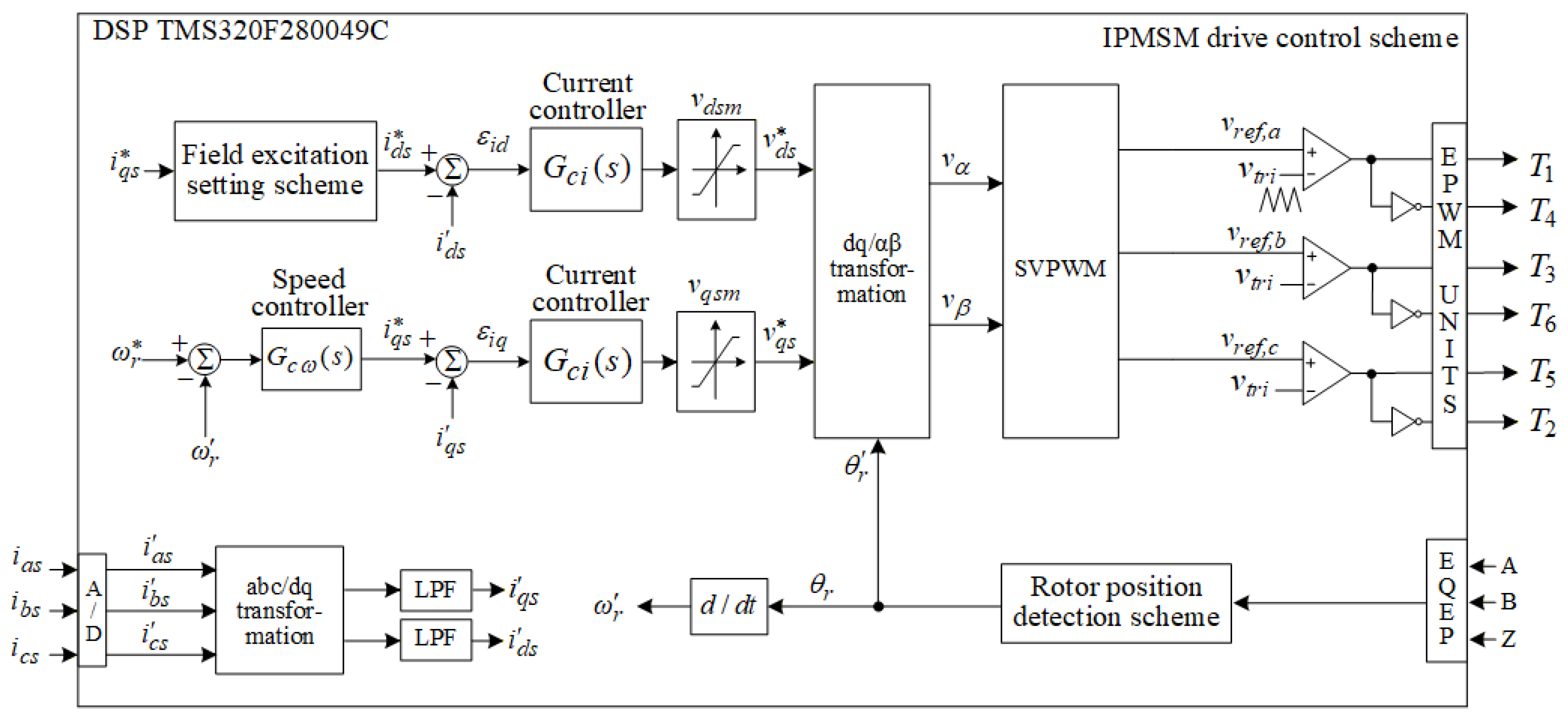
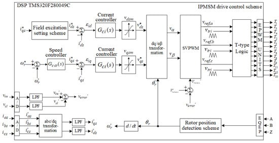
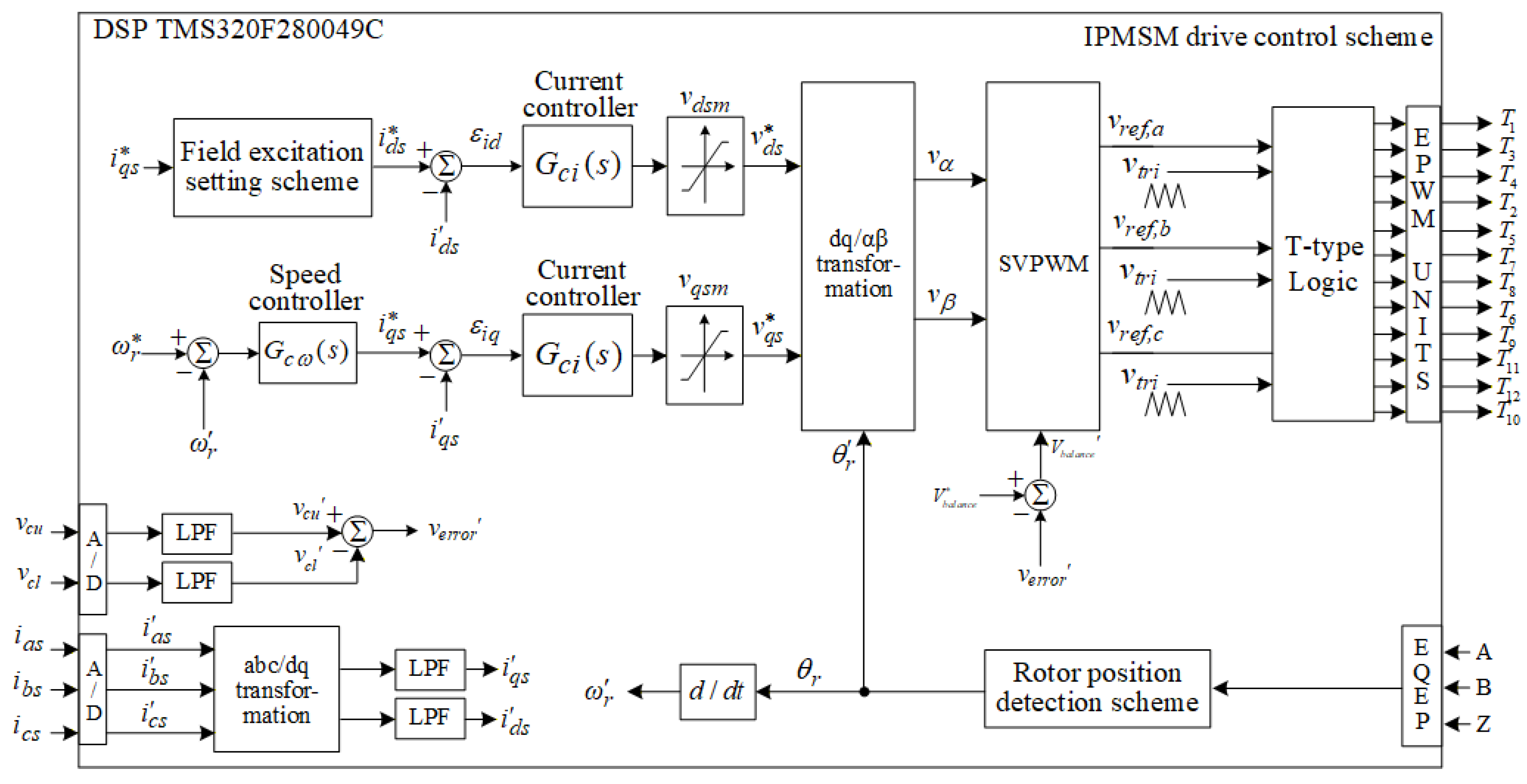
The firmware control architecture of the two-level inverter-fed IPMSM drive system is shown in Figure 8. The FOC and SVPWM algorithms are integrated with the ADC, eQEP, and ePWM peripherals to achieve closed-loop motor-drive control. Based on this verified framework, the firmware is extended to the T-type three-level inverter by incorporating the proposed carrier-based three-level SVPWM and neutral-point voltage balancing control, as shown in Figure 9.
Figure 8.
Firmware control architecture of the two-level inverter-fed IPMSM drive system.
Figure 9.
Firmware control architecture of the T-type three-level inverter-fed IPMSM drive system.
5.2. PWM Protection Logic
In each T-type phase leg, four switches are driven by two complementary PWM pairs. The conventional dead-band submodules can prevent simultaneous conduction within each complementary pair, thereby avoiding the forbidden combinations of – and –. However, the cross-pair combination of and cannot be directly protected by the standard dead-band function. Simultaneous conduction of these two switches creates a direct DC-link shoot-through path. Therefore, additional software- and hardware-based protection mechanisms are implemented to ensure safe commutation of the T-type inverter.
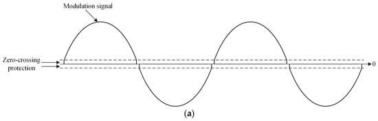
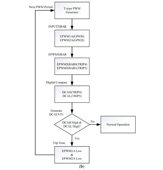
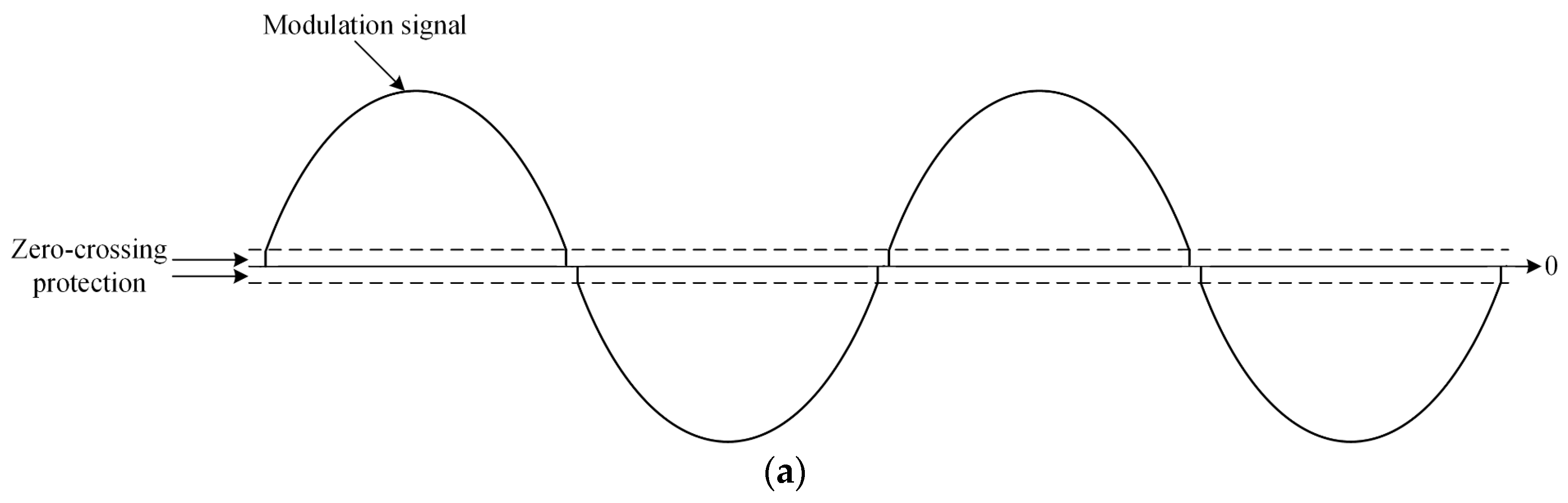
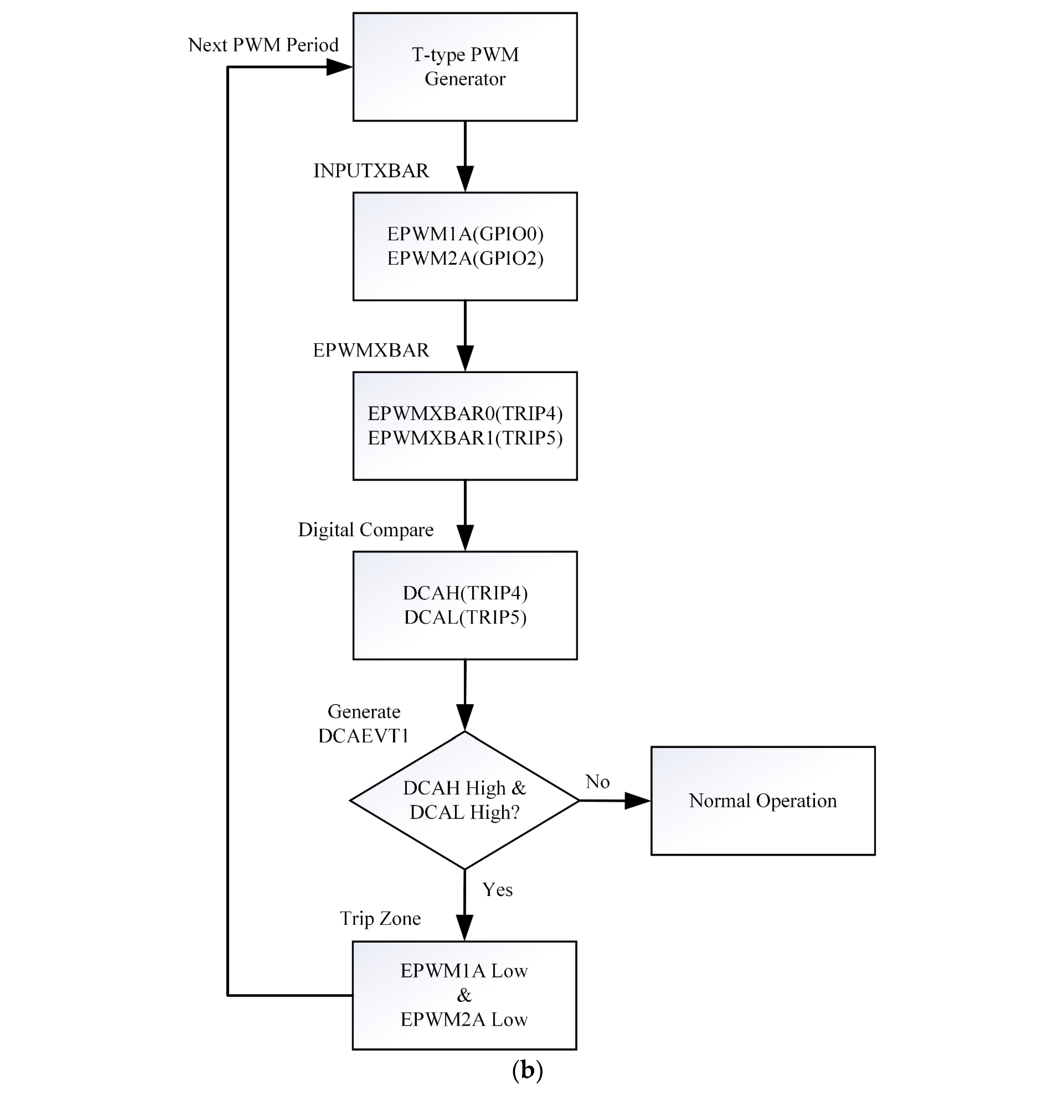
As the first protection layer, a software-based zero-crossing mechanism is implemented. As shown in Figure 10a, a hysteresis band is introduced around the zero-crossing point of the modulation signal. When the reference falls within this region, the phase leg is forced into State O, ensuring that the voltage-state transition follows P → O → N or N → O → P rather than directly switching between States P and N. As the second protection layer, a hardware interlock is implemented using the DSP Input X-BAR, Digital Compare, and ePWM Trip-Zone modules. As illustrated in Figure 10b, the and drive signals are continuously monitored. If simultaneous high-level signals are detected, the Trip-Zone module immediately disables the corresponding ePWM output without CPU intervention. The cycle-by-cycle protection mode allows normal switching to resume automatically after the abnormal condition is cleared.
Figure 10.
Two-layer protection scheme for the T-type inverter: (a) Software-based zero-crossing protection of the modulation signal; (b) hardware interlock implemented using the DSP digital-comparator and ePWM trip-zone modules.
6. Experimental Results of the Proposed IPMSM Drive System
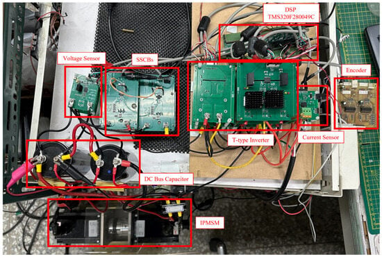
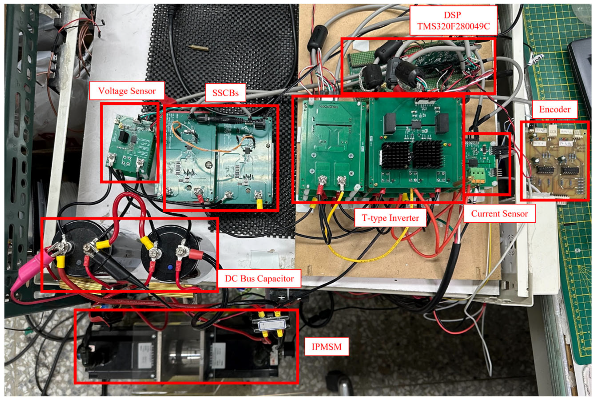
A 2.2 kW experimental platform is constructed to validate the proposed IPMSM drive system, as shown in Figure 11. The setup includes a DSP, a modular inverter, DC-link capacitors, solid-state circuit breakers, voltage and current sensors, an encoder, an IPMSM, and an IPMSG load machine. The inverter is implemented using separate half-bridge and auxiliary boards, allowing the same DSP and motor platform to be configured for both two-level and T-type inverter operation. The gate-drive parameters selected from the DPT results are adopted in the experimental inverter.
Figure 11.
Photograph of the experimental setup for the T-type inverter-fed IPMSM drive system.
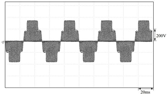
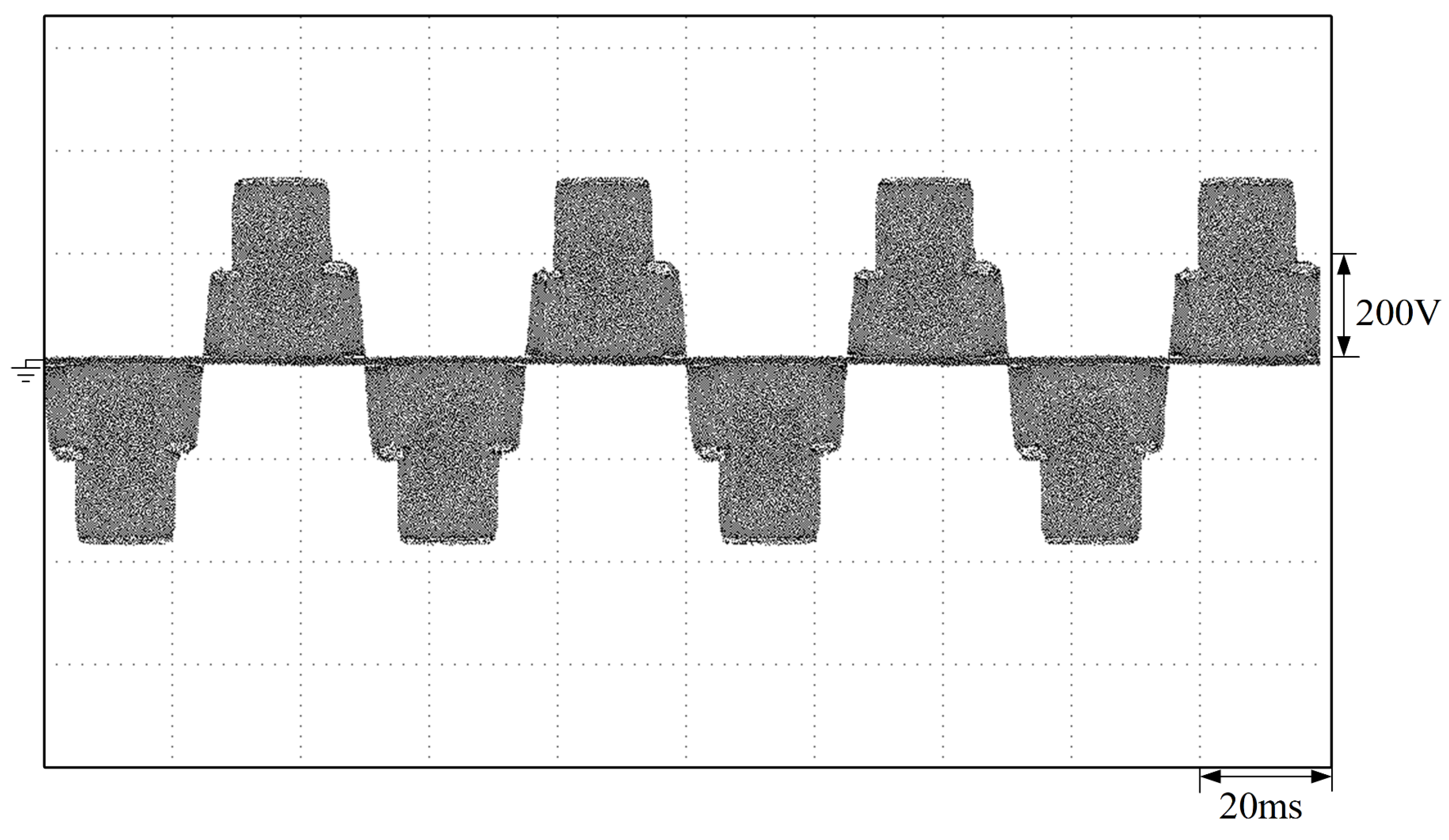
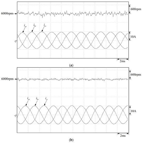
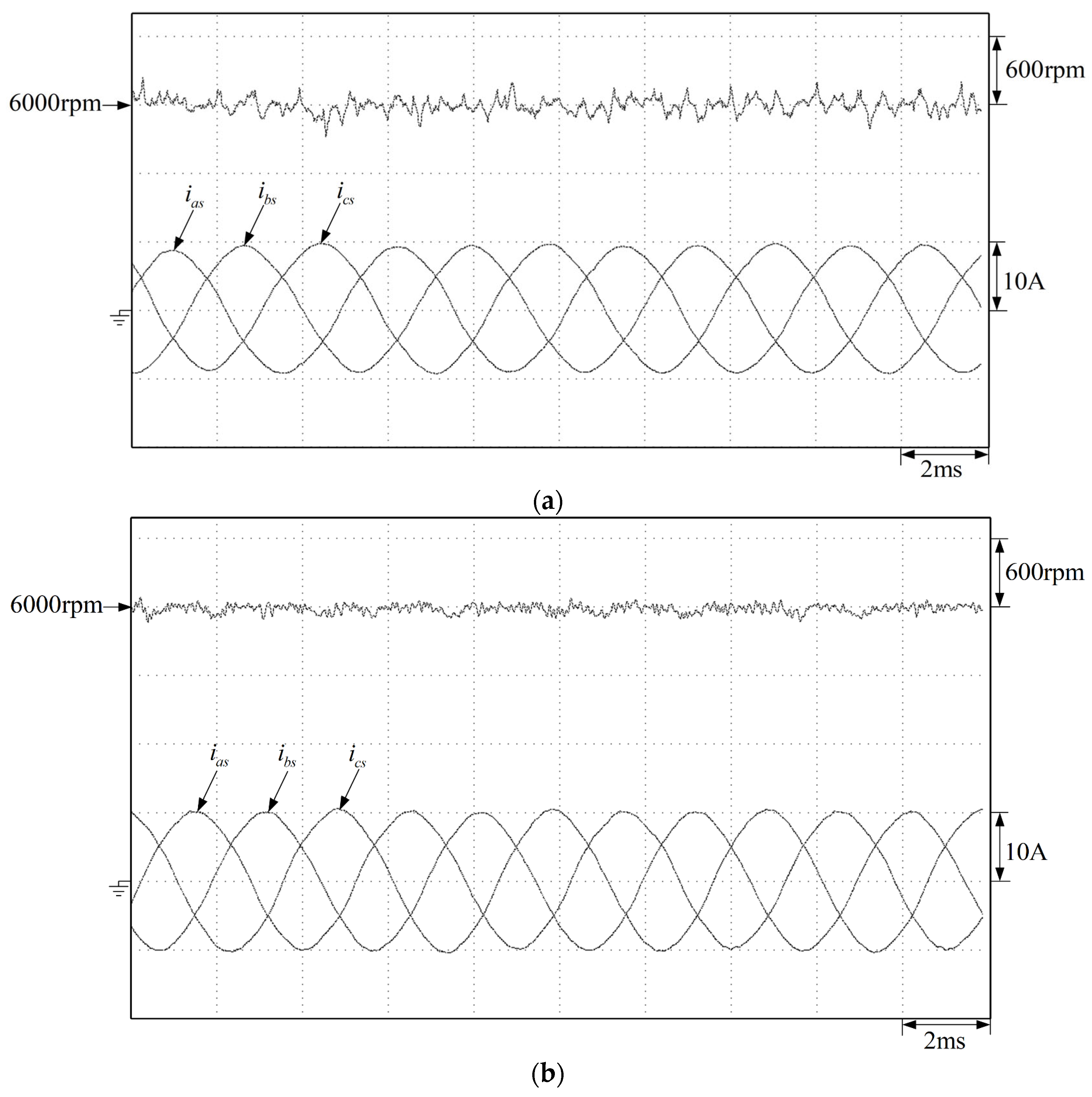
The measured line-to-line voltage of the T-type inverter is shown in Figure 12. Five distinct voltage levels are observed, verifying the correct operation of the proposed carrier-based three-level SVPWM and voltage-level assignment logic. The motor-drive performance is further evaluated at the rated operating condition of 6000 rpm and 2.2 kW. As shown in Figure 13, both inverter configurations maintain stable motor speed and balanced three-phase currents under full-load operation.
Figure 12.
Measured five-level line-to-line voltage of the T-type inverter.
Figure 13.
Measured steady-state waveforms at 6000 rpm and 2.2 kW under full-load operation: (a) Two-level inverter; (b) T-type inverter.
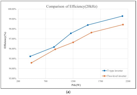
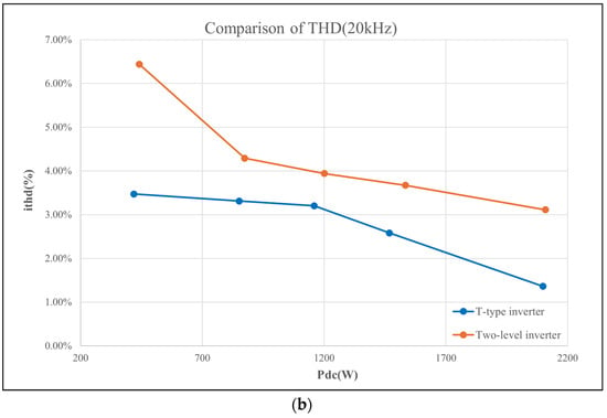
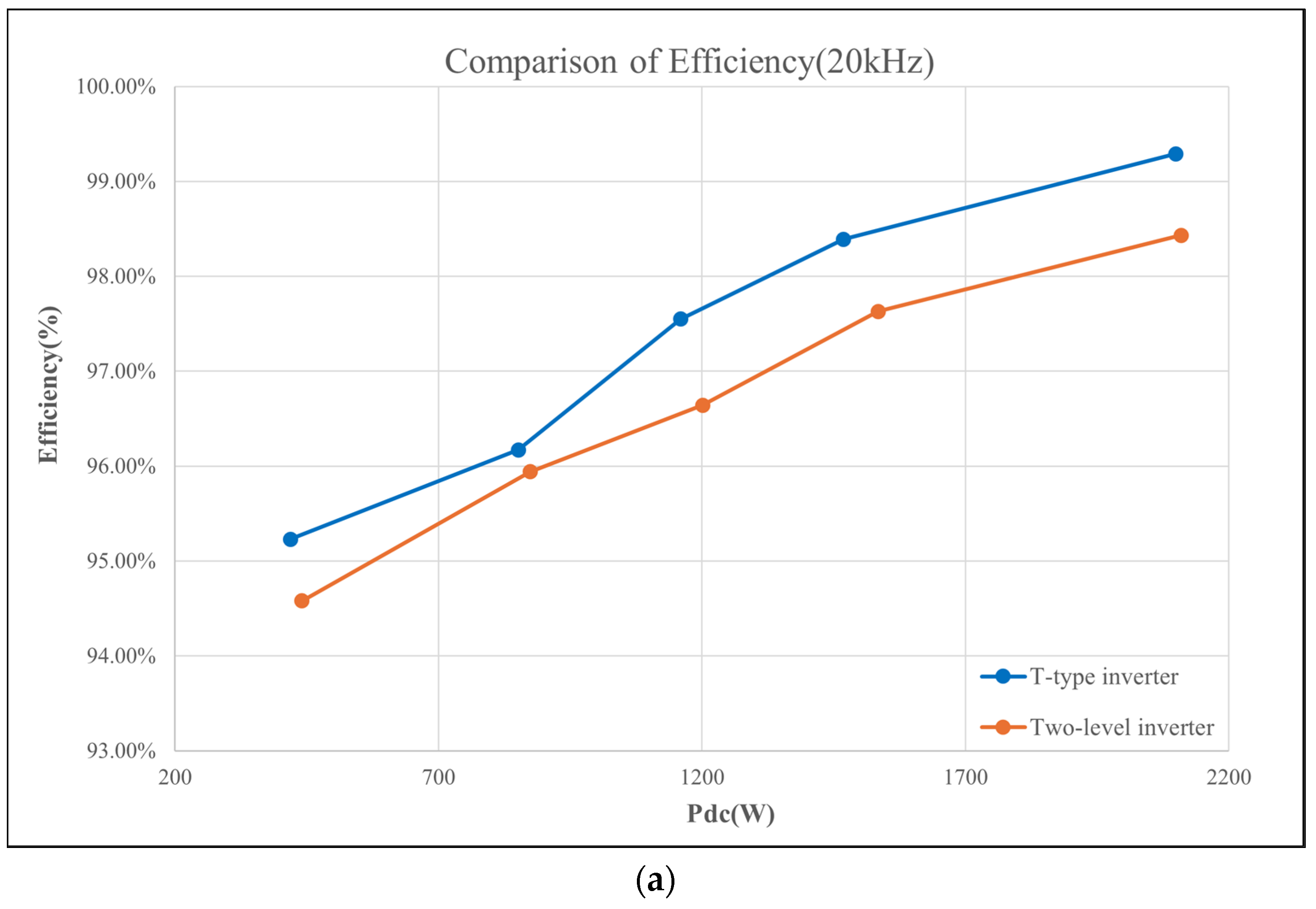
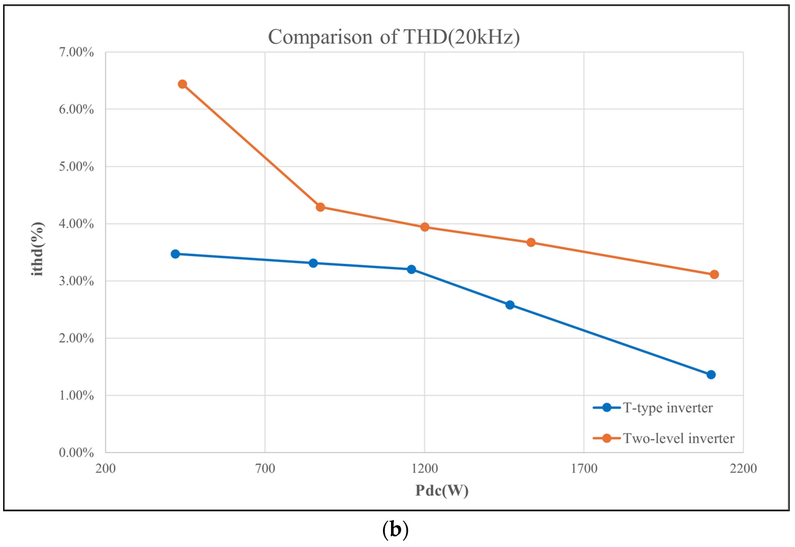
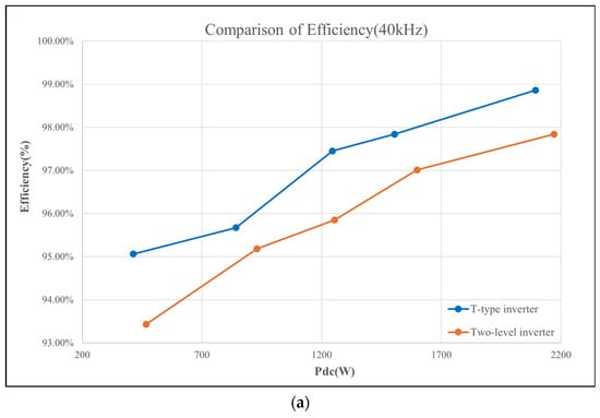
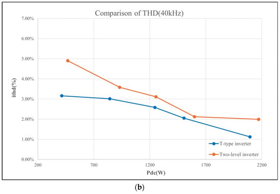
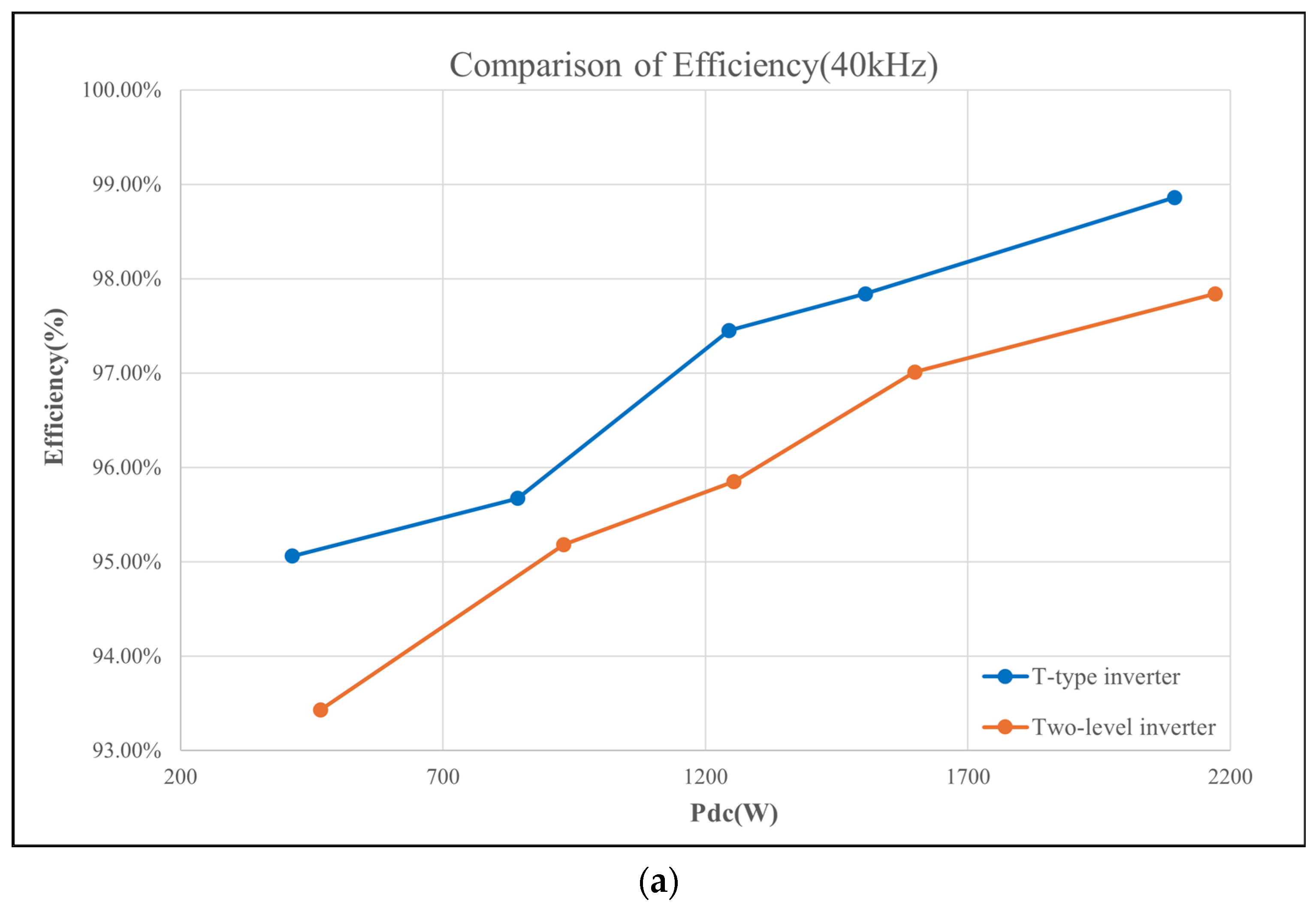
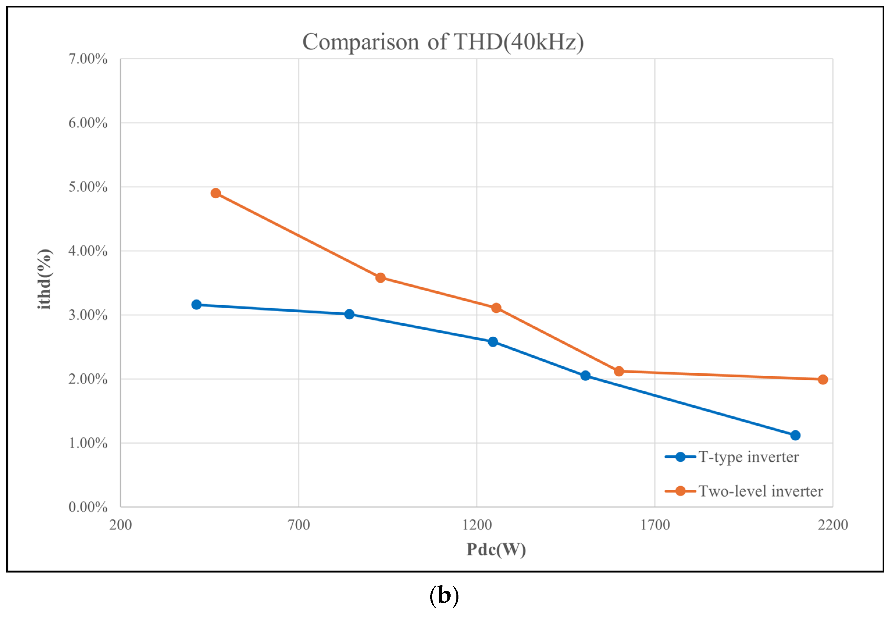
After stable operation is confirmed, the inverter efficiency and phase-current THD are compared under various load conditions at switching frequencies of 20 kHz and 40 kHz, as shown in Figure 14 and Figure 15, respectively. The T-type inverter generally achieves higher efficiency and lower current THD than the conventional two-level inverter at both switching frequencies. The efficiency improvement is mainly attributed to the reduced switching losses associated with smaller voltage transitions, while the lower THD results from the reduced output-voltage step of the three-level topology.
Figure 14.
Measured performance comparison between the proposed T-type and conventional two-level inverters at 20 kHz: (a) Inverter efficiency; (b) phase-current THD.
Figure 15.
Measured performance comparison between the proposed T-type and conventional two-level inverters at 40 kHz: (a) Inverter efficiency; (b) phase-current THD.
Specifically, under near full-load conditions at 20 kHz, the T-type inverter achieves 99.29% efficiency and 1.36% THD, outperforming the two-level baseline, which operates at 98.43% efficiency and 3.11% THD. At 40 kHz, its high-frequency advantage becomes more pronounced. The T-type topology achieves 98.86% efficiency compared to the two-level’s 97.84%, and it further suppresses the THD to 1.12% compared to the two-level’s 1.99%. These quantitative results explicitly demonstrate the proposed architecture’s ability to minimize switching losses and improve waveform quality.
7. Conclusions
This paper presents a 2.2 kW SiC-based T-type three-level inverter for high-efficiency IPMSM drive applications. A simplified carrier-based SVPWM strategy combined with active neutral-point voltage balancing is developed and verified through PLECS simulations. The switching characteristics of the adopted SiC MOSFETs are evaluated using a double-pulse test platform, while the control algorithms and protection functions are implemented on a TMS320F280049C DSP. Experimental validation is conducted at switching frequencies of 20 kHz and 40 kHz. The results confirm that the proposed T-type inverter achieves higher conversion efficiency and lower phase-current THD than the conventional two-level inverter under various load conditions. This improvement is attributed to the reduced switching voltage stress and smaller output-voltage steps of the three-level topology. Across all tested operating points, the inverter efficiency remains above 95%, while the phase-current THD is maintained below 4%. Specifically, under near full-load conditions, the T-type inverter achieves an outstanding peak efficiency of 99.29% at 20 kHz. Furthermore, at the higher switching frequency of 40 kHz, it significantly suppresses the THD to 1.12%. These results demonstrate the effectiveness and practical feasibility of the developed system for high-efficiency electric vehicle drive applications. Future investigations will focus on conducting comprehensive dynamic motor drive experiments, exploring thermomechanical considerations for high-density co-packaged inverter-motor integrations and extending the comparative analysis to other advanced multilevel architectures, such as the Active Neutral-Point-Clamped (ANPC) topology.
Author Contributions
Conceptualization, Y.-C.C.; methodology, C.-R.H. and P.-Y.L.; software, C.-R.H. and P.-Y.L.; validation, C.-R.H. and P.-Y.L.; formal analysis, C.-R.H.; investigation, C.-R.H.; resources, Y.-C.C.; data curation, C.-R.H.; writing—original draft preparation, C.-R.H.; writing—review and editing, Y.-C.C. and P.-Y.L.; visualization, C.-R.H.; supervision, Y.-C.C.; project administration, Y.-C.C.; funding acquisition, Y.-C.C. All authors have read and agreed to the published version of the manuscript.
Funding
This research was funded by the National Science and Technology Council (NSTC), Taiwan, grant number NSTC 115-2221-E-007-102.
Data Availability Statement
The original contributions presented in this study are included in the article. Further inquiries can be directed to the corresponding author.
Conflicts of Interest
The authors declare no conflicts of interest.
Abbreviations
The following are the abbreviations used in this manuscript.
| IPMSM/IPMSG | Interior Permanent Magnet Synchronous Motor/Generator |
| FOC | Field-Oriented Control |
| SVPWM | Space-Vector Pulse-Width Modulation |
| WBG | Wide-BandGap |
| DPT | Double-Pulse Test |
| DSP | Digital Signal Processor |
| THD | Total Harmonic Distortion |
| IM | Induction Motor |
| Si | Silicon |
| SiC | Silicon Carbide |
| GaN | Gallium Nitride |
| NPC | Neutral-Point-Clamped |
| VSIs | Voltage-Source Inverters |
References
- Chan, C.C.; Bouscayrol, A.; Chen, K. Electric, Hybrid, and Fuel-Cell Vehicles: Architectures and Modeling. IEEE Trans. Veh. Technol. 2010, 59, 589–598. [Google Scholar] [CrossRef] [Scilit]
- Aghabali, I.; Bauman, J.; Kollmeyer, P.J.; Wang, Y.; Bilgin, B.; Emadi, A. 800-V Electric Vehicle Powertrains: Review and Analysis of Benefits, Challenges, and Future Trends. IEEE Trans. Transp. Electrif. 2021, 7, 927–948. [Google Scholar] [CrossRef] [Scilit]
- de Santiago, J.; Bernhoff, H.; Ekergård, B.; Eriksson, S.; Ferhatovic, S.; Waters, R.; Leijon, M. Electrical Motor Drivelines in Commercial All-Electric Vehicles: A Review. IEEE Trans. Veh. Technol. 2012, 61, 475–484. [Google Scholar] [CrossRef] [Scilit]
- Chan, C.C.; Chau, K.T. An advanced permanent magnet motor drive system for battery-powered electric vehicles. IEEE Trans. Veh. Technol. 1996, 45, 180–188. [Google Scholar] [CrossRef]
- Zhang, D.; Zhang, H.; Li, X.; Zhao, H.; Zhang, Y.; Wang, S.; Ahmad, T.; Liu, T.; Shuang, F.; Wu, T. A PMSM Control System for Electric Vehicle Using Improved Exponential Reaching Law and Proportional Resonance Theory. IEEE Trans. Veh. Technol. 2023, 72, 8566–8578. [Google Scholar] [CrossRef] [Scilit]
- Kommuri, S.K.; Defoort, M.; Karimi, H.R.; Veluvolu, K.C. A Robust Observer-Based Sensor Fault-Tolerant Control for PMSM in Electric Vehicles. IEEE Trans. Ind. Electron. 2016, 63, 7671–7681. [Google Scholar] [CrossRef] [Scilit]
- Feng, G.; Lai, C.; Iyer, K.L.V.; Kar, N.C. Improved High-Frequency Voltage Injection Based Permanent Magnet Temperature Estimation for PMSM Condition Monitoring for EV Applications. IEEE Trans. Veh. Technol. 2018, 67, 216–225. [Google Scholar] [CrossRef] [Scilit]
- Shi, Z.; Sun, X.; Cai, Y.; Yang, Z.; Lei, G.; Guo, Y.; Zhu, J. Torque Analysis and Dynamic Performance Improvement of a PMSM for EVs by Skew Angle Optimization. IEEE Trans. Appl. Supercond. 2019, 29, 1–5. [Google Scholar] [CrossRef] [Scilit]
- Li, B.; Li, Q.; Lee, F.C.; Liu, Z.; Yang, Y. A High-Efficiency High-Density Wide-Bandgap Device-Based Bidirectional On-Board Charger. IEEE J. Emerg. Sel. Top. Power Electron. 2018, 6, 1627–1636. [Google Scholar] [CrossRef] [Scilit]
- Lee, W.; Li, S.; Han, D.; Sarlioglu, B.; Minav, T.A.; Pietola, M. A Review of Integrated Motor Drive and Wide-Bandgap Power Electronics for High-Performance Electro-Hydrostatic Actuators. IEEE Trans. Transp. Electrif. 2018, 4, 684–693. [Google Scholar] [CrossRef] [Scilit]
- Loncarski, J.; Monopoli, V.G.; Leuzzi, R.; Cupertino, F. Operation Analysis and Comparison of T-type NPC Si IGBT and SiC MOSFET Inverter-Based Highspeed Drives. In Proceedings of the IECON 2019—45th Annual Conference of the IEEE Industrial Electronics Society, Lisbon, Portugal, 14–17 October 2019; pp. 3154–3159. [Google Scholar]
- Millán, J.; Godignon, P.; Perpiñà, X.; Pérez-Tomás, A.; Rebollo, J. A Survey of Wide Bandgap Power Semiconductor Devices. IEEE Trans. Power Electron. 2014, 29, 2155–2163. [Google Scholar] [CrossRef] [Scilit]
- Cherif, O.M.; Nadji, B.; Tadjer, S.A.; Bencherif, H. Double Pulse Test Bench Design Methodology for Power Electronics Applications. In Proceedings of the 2024 12th International Conference on Systems and Control (ICSC), Batna, Algeria, 3–5 November 2024; pp. 190–196. [Google Scholar] [CrossRef] [Scilit]
- Yao, T.; Ayyanar, R. A Multifunctional Double Pulse Tester for Cascode GaN Devices. IEEE Trans. Ind. Electron. 2017, 64, 9023–9031. [Google Scholar] [CrossRef] [Scilit]
- Kar, A.; Manna, S.; Sengupta, M.; Banerjee, G. Design, Fabrication and Testing of gate driver and Double Pulse Test board for SiC MOSFETs. In Proceedings of the 2021 National Power Electronics Conference (NPEC), Bhubaneswar, India, 15–17 December 2021; pp. 1–6. [Google Scholar] [CrossRef] [Scilit]
- Emon, A.I.; Yuan, Z.; Deshpande, A.; Peng, H.; Paul, R.; Luo, F. A 1200V/650V/160A SiC+Si IGBT 3-Level T-type NPC Power Module with Optimized Loop Inductance. In Proceedings of the 2020 IEEE Energy Conversion Congress and Exposition (ECCE), Detroit, MI, USA, 11–15 October 2020; pp. 717–722. [Google Scholar] [CrossRef] [Scilit]
- Häring, J.; Hepp, M.; Wondrak, W.; Bakran, M.-M. A Neutral Point Balancing and Voltage Error Compensation Approach for Fault-Tolerant 3-Level Inverters. IEEE Open J. Power Electron. 2024, 5, 106–122. [Google Scholar] [CrossRef] [Scilit]
- Panda, A.; Dyanamina, G.; Singh, R.K. MATLAB Simulation of Space Vector Pulse Width Modulation for 3-level NPC Inverter and 2-level Inverter. In Proceedings of the 2021 International Conference on Sustainable Energy and Future Electric Transportation (SEFET), Hyderabad, India, 21–23 January 2021; pp. 1–5. [Google Scholar] [CrossRef] [Scilit]
- Schweizer, M.; Kolar, J.W. Design and Implementation of a Highly Efficient Three-Level T-Type Converter for Low-Voltage Applications. IEEE Trans. Power Electron. 2013, 28, 899–907. [Google Scholar] [CrossRef] [Scilit]
- Nemade, R.V.; Pandit, J.K.; Aware, M.V. Reconfiguration of T-Type Inverter for Direct Torque Controlled Induction Motor Drives Under Open-Switch Faults. IEEE Trans. Ind. Appl. 2017, 53, 2936–2947. [Google Scholar] [CrossRef]
- Bhattacharya, S.; Mascarella, D.; Joós, G.; Cyr, J.-M.; Xu, J. A Dual Three-Level T-NPC Inverter for High-Power Traction Applications. IEEE J. Emerg. Sel. Top. Power Electron. 2016, 4, 668–678. [Google Scholar] [CrossRef] [Scilit]
- Roy, P.; Bandyopadhyay, A. Control of a Three-Level T-Type Inverter-Fed PMSM with Regenerative Braking Tested with Dynamometer Test Bench Emulation and EV Load. IEEE Trans. Transp. Electrif. 2026, 12, 487–498. [Google Scholar] [CrossRef] [Scilit]
- Huang, C.-R.; Chang, Y.-C.; Lin, P.-Y. Development and Performance Analysis of a High-Efficiency Interior Permanent Magnet Synchronous Motor Drive System Based on a T-type Three-Level Inverter. In Proceedings of the 9th International Conference on Knowledge Innovation and Invention 2026 (ICKII 2026), Sendai, Japan, 14–16 August 2026. [Google Scholar]

Disclaimer/Publisher’s Note: The statements, opinions and data contained in all publications are solely those of the individual author(s) and contributor(s) and not of MDPI and/or the editor(s). MDPI and/or the editor(s) disclaim responsibility for any injury to people or property resulting from any ideas, methods, instructions or products referred to in the content. |
© 2026 by the authors. Licensee MDPI, Basel, Switzerland. This article is an open access article distributed under the terms and conditions of the Creative Commons Attribution (CC BY) license.