


Abstract
Perovskite tandem solar cells (TSCs) have emerged as a transformative photovoltaic technology, offering a viable pathway to surpass the Shockley-Queisser limit of single-junction devices by enabling broader solar spectrum utilization and reduced thermalization losses. This review provides a comprehensive overview of recent progress in perovskite-based TSCs, covering four major device architectures: perovskite/silicon, perovskite/CIGS, all-perovskite, and perovskite/organic TSCs. We systematically discuss the fundamental working principles, including bandgap engineering, charge generation and separation, and current-voltage matching, followed by an in-depth analysis of strategies for perovskite layer regulation, interface engineering, and transport-layer optimization. Key advancements, such as compositional engineering, defect passivation, crystallization control, and optical management, have synergistically pushed power conversion efficiencies (PCEs) beyond 34% for perovskite/silicon TSCs and over 28% for all-perovskite and perovskite/organic configurations. Despite these achievements, critical challenges remain, including material instability, halide phase segregation, lead toxicity, scalable fabrication, and cost-effective integration. This review also outlines future perspectives, emphasizing the development of lead-free perovskites, novel charge-transport materials, advanced encapsulation techniques, and large-area manufacturing processes. With continued interdisciplinary efforts, perovskite TSCs hold great promise for driving the global transition toward sustainable and low-carbon energy systems.
1. Introduction
The demand for clean and renewable energy sources has become increasingly urgent in the face of global climate change and the depletion of fossil fuels. Solar energy, as an abundant and sustainable resource, holds great promise for meeting the world’s energy needs. Photovoltaic (PV) technology, which converts sunlight directly into electricity, has witnessed significant progress in recent years. Among the various PV technologies, perovskite solar cells (PSCs) have emerged as a highly promising candidate due to their exceptional optoelectronic properties, low cost, and ease of fabrication. Perovskite materials, with the general formula ABX3, have shown remarkable performance in single-junction devices, achieving PCEs exceeding 26%. However, the theoretical PCE of single-junction solar cells is fundamentally restricted to 29.4% by the Shockley-Queisser (S-Q) limit [1]. To overcome this limitation, TSCs have been developed, which combine two or more semiconductor materials with complementary bandgaps to capture a broader spectrum of sunlight and minimize thermalization losses [2]. Perovskite materials are uniquely suited for TSCs due to their highly tunable bandgaps (1.2–2.3 eV), allowing them to function as ideal top-cell absorbers [3]. Beyond bandgap optimization and current matching, the long-term reliability of perovskite-based top cells is another critical factor determining their practical viability. Wide-bandgap (WBG) mixed-halide perovskites often suffer from light-induced halide phase segregation, which induces bandgap instability and substantial voltage losses during operation. Recent efforts have focused on enhancing their stability through compositional engineering, such as triple-halide alloying and incorporation of inorganic cations, as well as defect passivation and low-dimensional structural modulation to suppress ion migration pathways. In addition, methylammonium-free compositions and lattice reinforcement strategies based on strong intermolecular interactions have further improved thermal robustness. These advances demonstrate that engineered WBG perovskites can achieve enhanced operational stability under continuous illumination and elevated-temperature conditions, strengthening their role as promising top-cell absorbers for tandem architectures.
Among the various tandem configurations, perovskite/silicon TSCs have attracted the most significant research attention and have demonstrated the most impressive progress. Silicon PV technology, with its well-established manufacturing infrastructure, high efficiency, and proven long-term stability, provides an ideal bottom-cell platform. The combination of a WBG perovskite top cell with a silicon bottom cell has yielded remarkable results, with certified PCEs reaching 34.85% as of early 2026, substantially exceeding the theoretical limit of single-junction silicon devices [4]. Beyond conventional monofacial designs, bifacial tandem configurations that capture albedo light from the rear side have gained increasing interest, offering not only enhanced energy yield but also potential pathways for improved device stability through current-matching optimization [5]. In parallel, perovskite/Cu(In,Ga)Se2 (CIGS) TSCs offer a thin-film alternative with flexible substrate compatibility and high efficiency potential, while all-perovskite TSCs present the advantage of a unified material system, potentially simplifying fabrication and reducing costs. Furthermore, perovskite/organic TSCs have emerged as compelling low-temperature-processed alternatives, with recent studies demonstrating that rational sub-cell engineering, including molecular design of novel acceptors to form energetic alloys, can significantly optimize charge carrier dynamics and reduce energy losses within the tandem stack [6].
Despite these remarkable achievements, several critical challenges must be addressed before perovskite-based TSCs can be successfully commercialized. A major bottleneck lies in the WBG perovskite top cells, which often suffer from severe non-radiative recombination and light-induced halide phase segregation. These issues lead to substantial open-circuit voltage (Voc) deficits, limiting the device performance, and compromise the long-term operational stability of the entire tandem device [7]. Additionally, the design of efficient and robust interconnecting layers (ICLs) remains essential for ensuring low electrical resistance and high optical transparency between the sub-cells, as any inefficiencies in charge recombination or transport at these interfaces can result in significant performance losses [2]. The stability of perovskite materials under operational conditions, particularly in the presence of moisture, oxygen, heat, and continuous illumination, remains a formidable challenge for commercialization. Moreover, the scalability of fabrication processes from laboratory-scale devices to large-area modules, the toxicity concerns associated with lead-containing perovskites, and the economic competitiveness with established PV technologies all represent substantial hurdles that require innovative solutions.
This review aims to provide a comprehensive overview of the current status and recent progress of perovskite TSCs, including their fundamental working principles, diverse device architectures, and State-of-the-Art optimization strategies. We systematically examine the critical aspects of materials engineering, including compositional tuning, defect passivation, interface modification, and crystallization control for high-quality perovskite absorber layers. We also discuss the design and optimization of charge-transport layers (CTLs), ICLs, and transparent electrodes that are crucial for efficient carrier extraction and optical management. Furthermore, we highlight the key challenges associated with device stability, scalability, and lead toxicity, and offer perspectives on future research directions and commercialization pathways. Through this comprehensive analysis, we aim to provide valuable insights for researchers and engineers working toward the development of next-generation high-efficiency, stable, and cost-effective perovskite tandem PVs that can contribute meaningfully to the global transition toward sustainable energy. Figure 1 summarizes the working principles, device architectures, optimization strategies, and challenges of perovskite TSCs.
Figure 1.
Overview of perovskite TSCs, including working principles, device architectures, optimization strategies, and challenges.
2. Working Principles of Perovskite TSCs
2.1. Bandgap Engineering
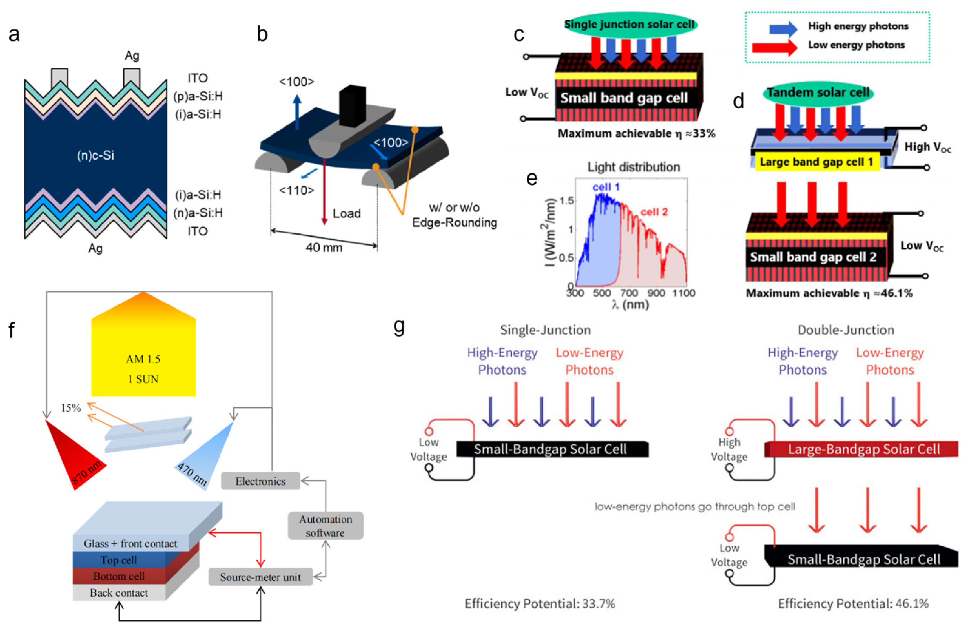
The key principle behind TSCs is the utilization of multiple semiconductor materials with different bandgaps to absorb different portions of the solar spectrum, thereby breaking through the S-Q efficiency limit of single-junction devices. In a single-junction solar cell, the S-Q limit restricts efficiency to ~33% due to transmission of low-energy photons and thermalization of high-energy photons. Photons with higher energy than the bandgap are absorbed but lose excess energy as heat, a loss mechanism called thermalization. TSCs minimize thermalization by using multiple absorbers, each responsible for a section of the solar spectrum. However, while tandem architectures intrinsically reduce thermalization losses through improved spectral utilization, additional loss pathways, such as interfacial recombination, may arise from the introduction of multiple sub-cell interfaces. Therefore, minimizing interfacial losses through optimized device architectures and interface engineering is essential to fully realize the theoretical efficiency advantages of TSCs. In a perovskite TSC, the top cell, typically made of a WBG perovskite material, absorbs the high-energy photons, while the bottom cell, made of a narrow-bandgap (NBG) material (such as Si or CIGS), absorbs the low-energy photons that are transmitted through the top cell. Theoretically, an optimal combination of ~1.9 eV for the top cell and ~1.0 eV for the bottom cell can achieve a PCE of up to ~42% (Figure 2c–e). By carefully selecting the bandgaps of the two materials, it is possible to maximize the absorption of sunlight across the entire solar spectrum, thereby increasing the PCE of the tandem cell. The bandgap of perovskite materials can be tuned by varying the composition of the A, B, and X components. For example, by substituting different organic or inorganic cations for the A-site, different divalent metal cations for the B-site, or different halide anions for the X-site, the bandgap of the perovskite can be adjusted within a wide range (Figure 2g). This tunability of the bandgap makes perovskite materials highly suitable for use in TSCs, as it allows for precise optimization of the optical absorption characteristics of the top cell to match the requirements of the tandem architecture [8].
2.2. Charge Generation and Separation
When sunlight is incident on a perovskite TSC, photons are absorbed by both the top and bottom cells, generating electron–hole pairs (excitons). In such a configuration, the perovskite top cell absorbs visible light but transmits infrared and near-infrared light to the bottom cell, enabling a large portion of the solar spectrum to be utilized. In perovskite materials, which exhibit steep absorption edge and exceptionally low sub-gap absorption, due to their strong optical absorption coefficients and high carrier mobility, the generated excitons can quickly dissociate into free electrons and holes. The electrons and holes are then separated by the built-in electric field at the heterojunction between the perovskite and the CTLs and are transported toward the respective electrodes. In a tandem cell, the WBG top cell generates a higher voltage from high-energy photons, while the NBG bottom cell generates a lower voltage from low-energy photons. The total voltage is the sum of the two sub-cells, but the current is limited by the lower of the two. Therefore, the charge transfer between the two sub-cells is a crucial process. To ensure efficient charge transfer, a recombination layer (RL) or an interconnecting layer is typically inserted between the two sub-cells. In a two-terminal monolithic tandem, directly connecting the n-layer of one sub-cell to the p-layer of the other would form a blocking p-n junction (Figure 2a,b). To resolve this, an RL or tunnel junction is inserted, which supports the flow of electrons from one sub-cell to the other. This layer serves to facilitate the transfer of holes from the bottom cell to the top cell, and electrons from the top cell to the bottom cell, while minimizing recombination losses. The design and properties of the RL play a vital role in determining the performance of the tandem cell, as any inefficiencies in charge transfer can lead to significant losses in PCE [9]. In particular, interfacial recombination at the connecting layers represents an additional non-radiative loss pathway, where photogenerated carriers are lost as heat rather than contributing to photocurrent. This loss mechanism is distinct from thermalization losses associated with photon-energy mismatch and must be minimized through careful interface engineering and RL optimization.
2.3. Current and Voltage Matching
In a TSC, the two sub-cells are connected in series, meaning that the current flowing through both sub-cells must be the same [10]. To achieve this, the optical absorption and charge generation in each sub-cell need to be carefully balanced to ensure that they produce the same amount of current under the same illumination conditions (Figure 2f). This process is known as current matching. If the current generated by one sub-cell is significantly higher than that of the other sub-cell, a phenomenon called current mismatch occurs, which can lead to a reduction in the PCE of the tandem device [11]. To avoid current mismatch, various strategies can be employed, such as optimizing the thickness and composition of the absorber layers in each sub-cell, adjusting the optical properties of the device through the use of antireflective coatings or light-trapping structures, and carefully selecting the bandgaps of the materials to ensure efficient absorption of different portions of the solar spectrum. In addition to current matching, voltage matching is also an important consideration in TSCs. The Voc of a tandem cell is the sum of the Voc values of the individual sub-cells. However, due to losses at the interfaces between the sub-cells and in the CTLs, the actual Voc of the tandem cell is usually lower than the sum of the Voc values of the sub-cells. To maximize the Voc of the tandem cell, it is essential to minimize these losses through the use of high-quality materials, optimized device architectures, and efficient CTLs [12].
Figure 2.
Schematic illustration of (a) the SHJ cell and (b) the test configuration. Reprint with permission [13]. Copyright 2026, Elsevier. Schematic illustration of (c) single-junction and (d) tandem solar cell. (e) Response of the top and bottom cells to the spectrum of light. Reprint with permission [9]. Copyright 2018, Elsevier. (f) Sketch of the current-matching machine (CMM) experimental setup. Reprint with permission [11]. Copyright 2013, IEEE. (g) Advantage of a TSC. Reprint with permission [11]. Copyright 2013, IEEE.
3. Device Architectures of Perovskite TSCs
3.1. Perovskite/Silicon TSCs
Perovskite/silicon TSCs are one of the most widely studied and promising architectures in the field of perovskite TSCs. In this architecture, a WBG perovskite top cell is stacked on top of an NBG silicon bottom cell. The silicon bottom cell, which is a well-established and highly efficient PV technology, provides a stable and reliable foundation for the tandem cell, while the perovskite top cell enables the absorption of high-energy photons that are not efficiently captured by the silicon cell. There are two main types of perovskite/silicon TSCs: monolithic and mechanically stacked. In monolithic perovskite/silicon TSCs, the perovskite and silicon sub-cells are grown directly on top of each other, sharing a common RL. This architecture offers the advantage of a simpler device structure and potentially higher efficiency, as it allows for more efficient charge transfer between the two sub-cells. However, the fabrication process of monolithic tandem cells is more challenging, as it requires precise control over the growth and interface properties of the two materials. In mechanically stacked perovskite/silicon TSCs, the perovskite and silicon sub-cells are fabricated separately and then mechanically stacked on top of each other. This architecture offers greater flexibility in terms of material selection and device design, as the two sub-cells can be optimized independently. However, the mechanical-stacking process can introduce additional optical and electrical losses, which can reduce the efficiency of the TSCs.
3.1.1. Perovskite-Layer Regulation
The performance of perovskite/silicon TSCs relies critically on the systematic regulation of the perovskite layer, which encompasses multiple interrelated dimensions: from material composition design, defect and interface passivation, and crystallization-process control to the final optical and electrical performance matching. These aspects are interconnected and progressively built upon one another, determining the ultimate efficiency and stability of the tandem devices.
Compositional engineering: A central objective of compositional engineering is the precise tuning of the perovskite bandgap by regulating ionic components. Early studies demonstrated that adjusting the Br−/I− ratio in FA0.9Cs0.1Pb(I1−xBrx)3 could widen the bandgap from 1.53 eV to 1.7 eV, enhancing stability and enabling efficient spectral filtering for four-terminal reflective tandem devices. Theoretical calculations further guided bandgap optimization: detailed balance limit analysis determined ideal top-cell bandgaps for different tandem architectures, while optoelectronic modeling enabled rational tuning of A-site cations and halide anions, supporting efficient current matching and high-efficiency tandem design. Guided by these theoretical and experimental foundations, mixed-cation/mixed-halide perovskites with precisely tuned bandgaps (e.g., 1.61 eV) were developed. Combined with buried interface modification using Al2O3 nanoparticles, these compositions improved crystallinity, suppressed interfacial recombination, and delivered high Voc and efficient performance under current-matched conditions [14,15,16,17]. A critical challenge for WBG perovskites is intrinsic halide phase segregation that degrades device performance. The fundamental origin of light-induced halide phase segregation in WBG mixed-halide perovskites arises from two synergistic driving forces: photogenerated charge accumulation distorts the Pb-X octahedral framework to generate local lattice strain, while thermodynamically favored halide ion migration redistributes I− and Br− across grain boundaries under continuous illumination. Light excitation weakens Pb-Br bonds preferentially, creating mobile halide vacancies that act as fast diffusion channels, eventually forming Br-rich and I-rich segregated domains with mismatched bandgaps. This spatial band fluctuation introduces severe non-radiative recombination centers and permanent Voc loss, which can be suppressed via lattice rigidification and halide ion immobilization strategies. The close correlation between photoinduced lattice strain, ionic mobility, and long-term phase instability has been systematically validated via seasonal outdoor stability measurements of n-i-p perovskite devices [18]. Two effective strategies have been established to address this issue. Lowering Br− content to tune the bandgap to 1.59–1.62 eV enables efficient current matching under bifacial irradiation by utilizing albedo to boost the silicon sub-cell current, which suppresses light-induced phase segregation and achieves certified efficiencies over 25% while balancing efficiency and stability. For applications requiring WBG perovskites, triple-halide (Cl/Br/I) alloying by incorporating MAPbCl3 into CsFA-based precursors promotes Cl incorporation via Br-mediated lattice contraction, significantly suppressing phase segregation, lowering defect density, and delivering a certified efficiency of 27% in 1 cm2 perovskite/silicon tandem devices [5,19,20]. Su et al. optimized MA-free WBG perovskites for 4-T perovskite/silicon TSCs. They screened Cs-FA-Br-I compositions to obtain a stable 1.65 eV bandgap system. Rb+ doping suppressed lattice strain and phase segregation, reduced defects, and prolonged carrier lifetime. The 4-T tandem device achieved 29.98% PCE [21]. Shen et al. fabricated a WBG CPRA layer via cesium formate spin coating, which enhances light in-coupling, pins the absorption edge at 1.68 eV for ideal current matching, and yields a champion PCE of 28.53% [22]. To mitigate toxicity and spectral mismatch in lead-free perovskites, gradient compositional tuning of X-site halides (I, Br, and Cl) modulates the CsSnX3 bandgap, enabling spectral complementarity between sub-cells for optimal current matching, achieving 33.03% efficiency [23]. Zhang et al. employed a halogen anion pre-homogenization strategy via co-evaporated PbIBr eutectic template to reduce nucleation disparity between iodide and bromide, enabling phase-separation-free WBG tuning (1.59–1.78 eV) and promoting homogeneous crystallization with minimized interface defects, achieving 30.83% PCE [24]. De Wolf et al. incorporated methylenediammonium dichloride to generate THTZ-H+ cations in situ, which reinforce lattice interactions through multidirectional N-H…I hydrogen bonding, thereby enhancing phase stability under light/heat and achieving 33.7% certified PCE [25]. Table 1 summarizes the compositional engineering strategies for perovskite/silicon TSCs. In summary, triple-halide multi-cation schemes outperform simple Br/I binary tuning, as they rigidify lattices to suppress phase segregation fundamentally. MA-free designs gain thermal stability but demand stricter deposition control, representing a trade-off between stability and fabrication tolerance.
Table 1.
Compositional engineering strategies and the PV parameters for perovskite/silicon TSCs.
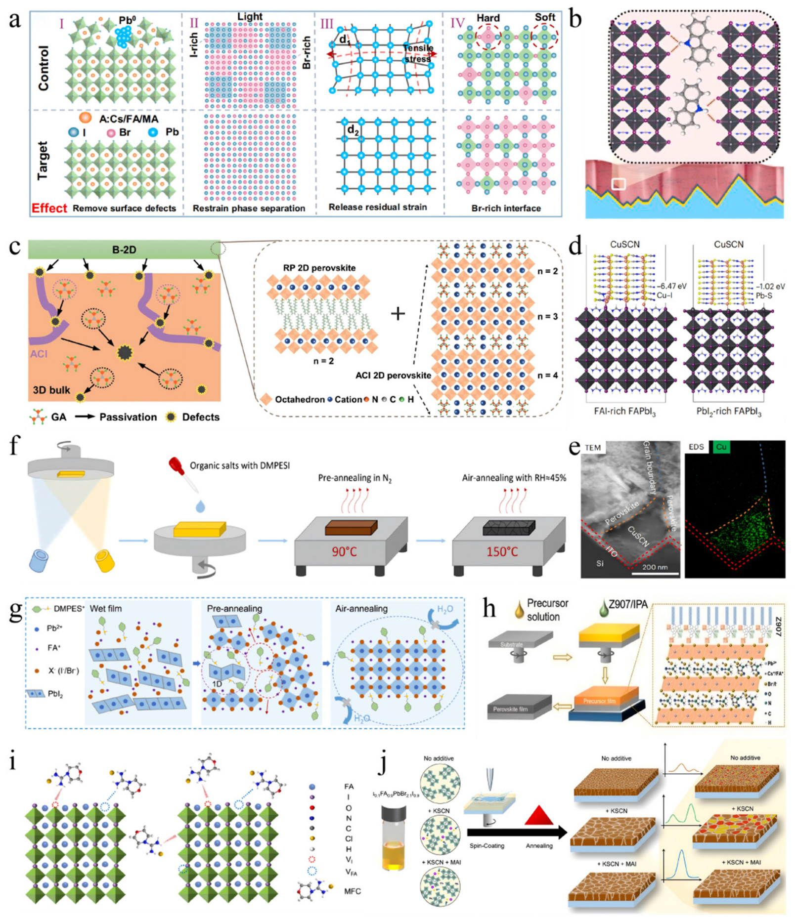
Defect and interface passivation: While compositional engineering optimizes the intrinsic electronic structure of perovskites, the inevitable defects (e.g., halide vacancies and grain boundary states) and interfacial recombination still limit tandem performance. Thus, targeted defect and interface passivation has become a key complementary strategy. The central objective of defect and interface passivation is to suppress non-radiative recombination and enhance operational stability, primarily achieved through strategic defect passivation and meticulous interface engineering. This approach focuses on precise defect targeting at the molecular level, with strategies ranging from small-molecule hydrogen bond donors to functionalized 2D additives, all designed to interact specifically with defect sites. Wolf et al. used carbazole molecules to form hydrogen-bonded networks at grain boundaries (Figure 3b), specifically passivating defects to suppress halide phase separation, which led to a certified PCE of 28.2% for perovskite/silicon TSCs [26]. For stubborn deep-level traps induced by iodine oxidation (forming I2), Yu et al. incorporated ammonium diethyldithiocarbamate (ADDC) into the perovskite precursor, which effectively reduced I2 to I−, suppressing deep-level traps and ion migration [27]. Shin et al. employed an anion-engineered 2D additive (PEA(I0.25SCN0.75)). The SCN− induces a conductive PbI2-based 2D phase at grain boundaries that simultaneously passivates defects and enhances charge transport, tackling both major limitations of WBG perovskites [28]. Aspartic acid (ASP) was employed as a double-charged additive to coordinate with PbI2, through which defects were passivated and non-radiative recombination was suppressed, yielding 30.68% PCE with 95% retention after 1900 h [29]. BD-Boc was introduced to coordinate with undercoordinated Pb2+ via carbonyl groups, by which crystallization kinetics were modulated and grain-boundary defects were passivated. Consequently, non-radiative recombination was suppressed and 28.47% efficiency was achieved in perovskite/silicon TSCs [30]. Overall, dual-functional molecular passivation is superior to single additives, repairing both bulk and grain-boundary defects. 2D/3D heterojunction passivation delivers the best long-term stability yet adds extra processing steps, limiting low-cost production.
Interface reconstruction and structured passivation: This category addresses both surface and interfacial defects through structural modification, including surface reconstruction, low-dimensional phase induction, and targeted surface coating, all aimed at forming a protective or passivating layer that eliminates defect sites. Wet chemical nano-polishing was employed to remove the defect-rich surface layer, and subsequent passivation with piperazinium iodide was applied, through which defects were eliminated, lattice strain was released, and interface energy alignment was optimized, thereby improving the perovskite/electron transport layer (ETL) interface (Figure 3a) [31]. By passivating bromine vacancies via PEABr surface coating, non-radiative recombination was suppressed, enabling 31% PCE in TSCs [32]. 4M-PEACI was used to induce a quasi-2D phase at grain boundaries, enabling regional defect encapsulation, which yielded 23.7% steady-state efficiency and 30.3% for 4T perovskite–silicon TSCs [33]. DMPESI reacted with PbI2 to form a 1D DMPESPbI3 phase, which accumulated at interfaces as a hydrophobic barrier, thereby suppressing moisture-induced decomposition (Figure 3f–g) [34].
Synergistic passivation strategies: These strategies integrate multiple mechanisms for comprehensive performance improvement. A KSCN-MAI synergistic strategy was employed, with K+ passivating defects, SCN− enlarging grains, and MAI removing residual SCN− via double displacement to suppress phase segregation, yielding 15.0% (single-junction) and 26.4% (triple-junction) PCEs (Figure 3j) [35]. Chen et al. adopted one-step post-treatment with mixed OAmI and GACl to simultaneously generate RP and ACI 2D perovskite phases, constructing gradient 2D/3D heterojunctions as described in the original work (Figure 3c). Macromolecular OAm+ cations only remain on the surface of the perovskite film to form Ruddlesden–Popper (RP) phases, while small GA+ ions can penetrate into the film interior at a depth of 150–300 nm to produce Alternating-Cation-Interlayer (ACI) phases. The content of the two phases gradually changes along the film thickness, enabling simultaneous passivation of both surface and bulk defects [36]. Zhang et al. incorporated MFC into the antisolvent. MFC formed strong hydrogen bonds with the perovskite, slowing crystallization and passivating defects, which enlarged grains and induced an n-type surface, yielding 30.65% PCE and 1.951 V Voc with enhanced stability (Figure 3i) [37].
Process-integrated passivation: Integrating passivation into fabrication processes has emerged as an efficient pathway. Vacuum-assisted solution treatment and GuaBr interface modification were combined to coordinately manage bulk and surface defects, yielding 19.67% PCE (1.22 V Voc) and 24.01% for TSCs [38]. Z907 was added into the antisolvent to form a self-assembled monolayer modulating crystallization (Figure 3a). -SCN/-COOH groups passivate defects and align interfacial energy, while hydrophobic chains enhance moisture resistance [39]. Post-treatment with FAI/mF-PEAI mixed solution was applied to slot-die-coated films, passivating iodine vacancies, reducing non-radiative recombination, and removing excess PbI2 to optimize charge transport, raising top-cell PCE from 16.14% to 20.79% [40]. Perovskite and CuSCN were co-deposited on textured silicon wafers. Cross-sectional TEM-EDS mapping (Figure 3e) directly demonstrates CuSCN enrichment at perovskite buried grain boundaries to build local hole-collecting contacts, while density functional theory (DFT) interfacial models (Figure 3d) confirm strong binding between CuSCN and uncoordinated Pb/I defects for suppressed non-radiative recombination and accelerated hole transport. This design delivers a certified efficiency of 31.46%, with 93.8% initial efficiency maintained after 1200 h (maximum power point) MPP tracking [41]. Table 2 summarizes the defect and interface passivation strategies for high-performance perovskite/silicon TSCs.
Table 2.
Defect and interface passivation strategies and the PV parameters for high-performance perovskite/silicon TSCs.
Figure 3.
(a) Schematic diagram of the changes in perovskite film before and after nano-polishing treatment. Reprint with permission [31]. Copyright 2024, Springer Nature. (b) Schematic illustration of interaction of carbazole with perovskite films. Reprint with permission [26]. Copyright 2021, Elsevier. (c) Schematic illustration of B-2D strategy. Reprint with permission [36]. Copyright 2024, Springer Nature. (d) Interfacial models of DFT calculations for CuSCN and FAIor PbI2-rich FAPbI3 (001) surfaces. Reprint with permission [41]. Copyright 2024, Springer Nature. (e) Cross-sectional high-angle annular dark-field TEM image. Reprint with permission [41]. Copyright 2024, Springer Nature. (f) Schematic of the hybrid two-step deposition method. Reprint with permission [34]. Copyright 2025, American Chemical Society. (g) Schematic diagram of the dynamic evolution of DMPESI molecules throughout the perovskite conversion pathway. Reprint with permission [34]. Copyright 2025, American Chemical Society. (h) Experiment procedures for the Z907 SAM-capped crystallization strategy. Reprint with permission [39]. Copyright 2024, Elsevier. (i) Schematic diagram of the interaction between MFC and the perovskite. Reprint with permission [37]. Copyright 2025, American Chemical Society. (j) Schematic diagram of the working mechanism of KSCN + MAI additive engineering. Reprint with permission [35]. Copyright 2024, Elsevier.
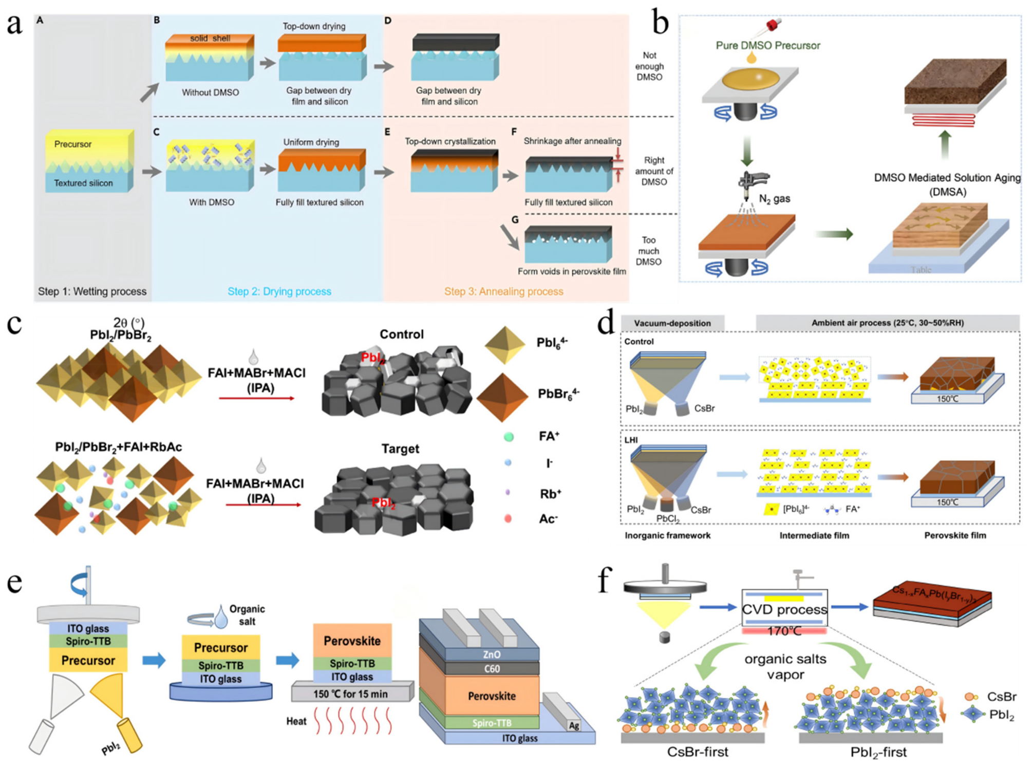
Deposition and crystallization control: Effective passivation only alleviates defects. The fundamental issue of poor film quality (small grains, pinholes, and uneven crystallization) on textured silicon substrates requires advanced deposition and crystallization control. Thus, process control to obtain high-quality, uniform perovskite films is essential for high-efficiency tandem devices, as it addresses the root cause and enables scalable fabrication. To achieve high-efficiency perovskite/silicon TSCs, scalable deposition techniques were developed for textured silicon substrates. Solvent engineering with nitrogen-knife-assisted blade coating enables void-free filling (Figure 4a), while slot-die coating with DMF-NMP optimized annealing reduces PbI2 aggregation, improving carrier lifetime and quasi-Fermi splitting to 25.2%. A two-stage vacuum flash method suppresses pinholes by sequential DMSO/DMF removal under controlled vacuum, yielding pinhole-free films and 22.5% PCE. For low-pressure CVD, Cs+ ions spontaneously migrate to achieve uniform vertical distribution regardless of precursor order. CsBr-first deposition accelerates conversion and widens the bandgap, enhancing charge transfer, leading to 18.7% (semi-transparent) and 26.9% (monolithic tandem) PCEs [42,43,44,45].
Additive design or template-guided growth was employed to optimize film morphology and crystallinity. Zhang et al. introduced FAI and RbAc into the PbI2/PbBr2 precursor to form a lead halide complex that regulates crystallization and promotes (100)-oriented grain growth (Figure 4c) [46]. Ballif et al. used a hybrid evaporation–spin-coating process. Co-evaporated PbI2/CsBr formed an inorganic template, followed by spin coating of FAI/MAI/MACl, inducing preferential (001) orientation with ~1 μm grains and reducing non-radiative recombination losses by 120 mV [47]. Zhang et al. co-evaporated CsCl with PbI2 to generate a δ-Cs0.3Pb4I8 intermediate phase that acts as a template for preferential black-phase growth, yielding denser films and 29.22% PCE (Figure 4e) [48]. Qiao et al. combined Pb(SCN)2 additive with air annealing, where Pb(SCN)2 promotes grain growth and air annealing, removes PbI2 impurities, and enhances crystallinity via moisture-assisted Ostwald ripening [49]. Chu et al. proposed DMSO-mediated solution aging with pure DMSO, nitrogen quenching, and Marangoni reflux to slow crystallization, producing uniform, low-stress, low-roughness WBG films that suppress halide segregation and improve transparency and carrier transport (Figure 4b) [50]. For crystal-nucleus control, Chen et al. employed OAmI-mediated nucleation with vacuum quenching to promote 3C cubic-phase nucleation and suppress Br-rich and 2H hexagonal phases, yielding 32.5% tandem PCE [51]. Schulze et al. introduced urea to lower the nucleation barrier for α-phase growth at low temperature, while excess urea migrated to the surface to passivate the perovskite/C60 interface, achieving 30.0% [52]. Xu et al. introduced PbCl2 via triple-source co-evaporation to form a longitudinal homogenized intermediate that slows crystallization and prevents capping-layer formation, enabling uniform interdiffusion under ambient air (Figure 4d) [53]. Table 3 summarizes the deposition and crystallization control for high-quality perovskite films. Vacuum evaporation yields large low-defect grains but costs more, while blade coating balances performance and scalability for industrialization. Additive-induced oriented growth is the most accessible low-cost route to improve film quality.
Table 3.
Deposition and crystallization control and the PV performance for high-quality perovskite films TSCs.
Figure 4.
(a) Mechanism of dense perovskite film formation. Reprint with permission [42]. Copyright 2020, Elsevier. (b) The preparation of WBG perovskite films. Reprint with permission [50]. Copyright 2024, Wiley-VCH GmbH. (c) PbI2/PbBr2 crystals and control perovskite film. Reprint with permission [46]. Copyright 2022, American Chemical Society. (d) Schematic of the LHI process. Reprint with permission [53]. Copyright 2024, American Chemical Society. (e) Preparation process of cesium salt/PbI2-based perovskite thin films. Reprint with permission [48]. Copyright 2024, Elsevier. (f) The schematic illustration of the low-pressure vapor deposition process for the perovskite film. Reprint with permission [45]. Copyright 2025, Wiley-VCH GmbH.
Optical management and current matching: Early strategies included nanophotonic tuning of perovskite thickness on textured silicon (optimal pyramid period, 450 nm) to match current density (20.6 mA/cm2), and bifacial design considering albedo, requiring thicker perovskite (0.55 μm) and 1.65–1.75 eV bandgap for matching, yielding >31.9% PCE [54,55]. Innovative electrode structures and bifacial illumination were employed. A quasi-finger-back-contact (QFBC) electrode (period, 750 nm; width ratio, 0.4) acted as a diffraction element to enhance short-wavelength absorption and transmit long-wavelength light, reducing series resistance and eliminating shading losses, thereby enabling 29.65% four-terminal PCE [56]. Furthermore, current-matching loss (CML) was quantified under dual-side illumination. Optimizing bandgap (~1.65 eV) and albedo minimized CML, achieving 1692 kW·h/m2 annual generation, 12.07% higher than single-sided devices [57].
Theoretical simulations guided parameter optimization. DFT and SCAPS-1D were used to determine CsGeI3’s suitable 1.6 eV bandgap and optimal thickness (265 nm), while controlling bulk/interface defects to minimize recombination, yielding 28.43% tandem PCE (Figure 5c) [58]. Similarly, SCAPS-1D optimized a tin-based perovskite (GA0.06(FA0.8Cs0.2)0.94SnI2Br) by adjusting thickness and defect density and selecting CTLs to suppress non-radiative recombination, achieving 32.12% (Figure 5f) [59]. Coordinated regulation of bandgap and thickness (e.g., 1.7 eV bandgap with increased thickness) enabled current matching and 32.71% efficiency [60]. Finally, a multiscale optical model with a genetic algorithm tuned photonic crystal parameters (lattice constants and side-wall angles) and perovskite thickness (465.5 nm) to enhance light trapping, achieving 32.07% efficiency, surpassing the original thick-device configuration (Figure 5e) [61]. Bifacial optical design optimizes current matching better than single-sided light trapping. Numerical simulation-guided bandgap-thickness tuning achieves theoretical current balance and higher energy output.
Figure 5.
(a,b) Influence of the period of the surface texture. Reprint with permission [54]. Copyright 2018, The Royal Society of Chemistry. (c) Schematic structure of CsGeI3-on-Si TSC (right). Reprint with permission [58]. Copyright 2024, Elsevier. (d) Jsc of top and bottom sub-cells. Reprint with permission [60]. Copyright 2024, Elsevier. (e) Variation in the perovskite layer thickness and maximum achievable photocurrent density (JMAPD). Reprint with permission [61]. Copyright 2025, Elsevier. (f) The energy-level alignment of the absorber layer. Reprint with permission [59]. Copyright 2024, Elsevier.
3.1.2. Interface-Regulation Strategies
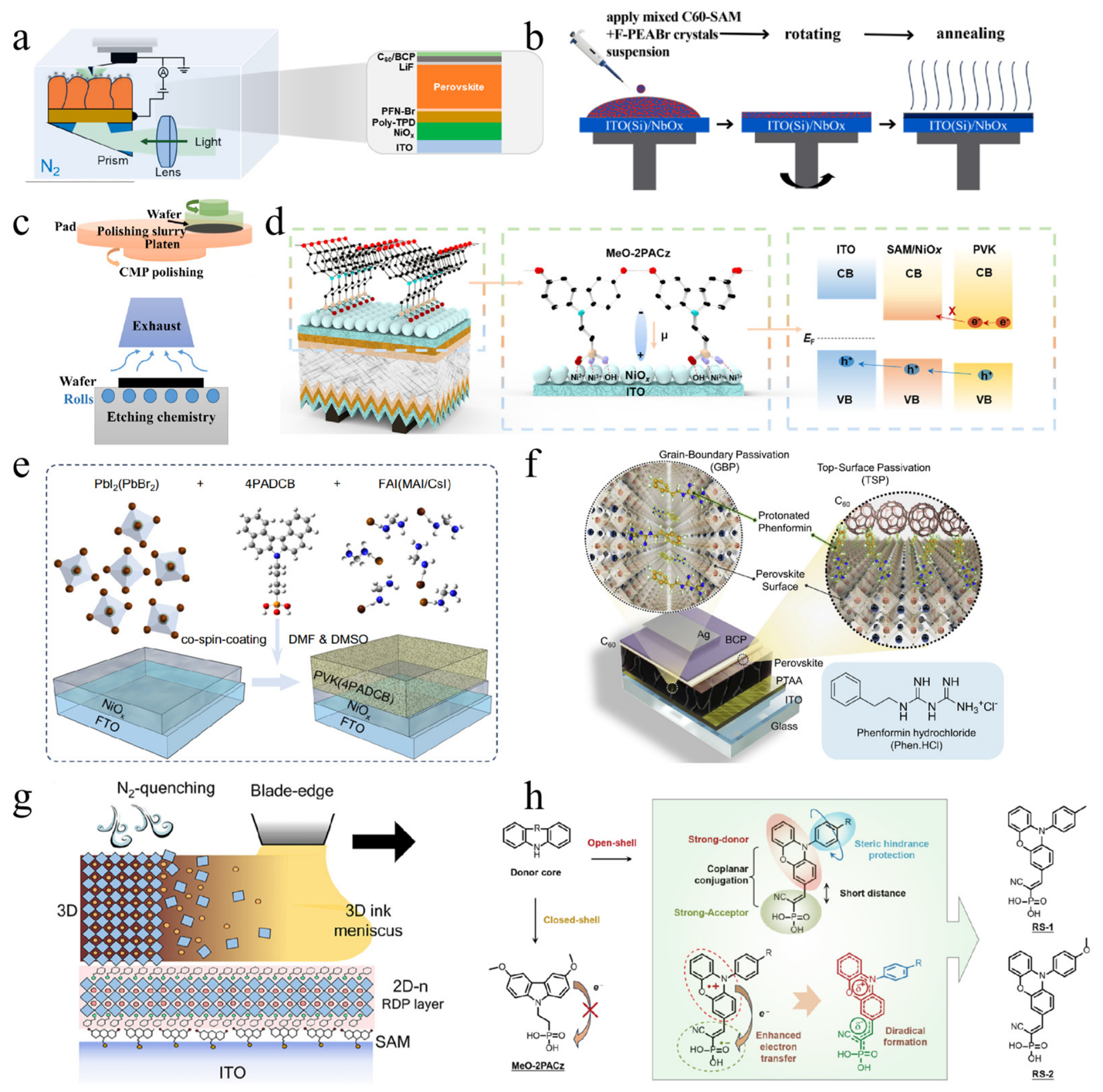
Interface-regulation strategies were developed to suppress non-radiative recombination and optimize carrier extraction. A hybrid two-step deposition with an nc-Si:H recombination junction improved shunt resistance, achieving 25.2% [62]. NiI2 was used to fill iodine vacancies via stronger Ni-I bonds, reducing interfacial recombination [63]. An ultrathin ITO interlayer (1.7 nm) enabled efficient carrier recombination and suppressed shunting, yielding 27.2% PCE [64]. LiF (2 nm) acted as a physical barrier and improved wettability, leading to 25.1% on 24 cm2 (Figure 6c) [65]. Mesoporous Al2O3 regulated ion distribution and converted the buried interface to p-type, forming a homojunction that enhanced the built-in field, giving 29.04% PCE [66]. A NiOx/MeO-2PACz hybrid improved SAM uniformity and energy alignment, resulting in 28.47% PCE with 81.8% FF (Figure 6d) [67]. A dual-layer LiF + EDAI combined field-effect and chemical passivation, enabling a certified PCE of 33.89% [68]. Oblique-angle deposited SiOx provided chemical (Pb=O) and field-effect passivation via an n/n+ homojunction, achieving 30.2% PCE [69]. AZO nanoparticles replaced atomic layer deposition (ALD), protecting the perovskite and promoting charge transport, yielding 25.3% PCE [70].
Vacancy defects and grain boundary traps within the perovskite layer, as well as energy-level offsets between perovskite and transport layers/silicon substrates, often lead to severe non-radiative recombination and hindered carrier extraction, directly limiting device efficiency and stability. To address this, research teams have developed diversified strategies, ranging from self-assembled monolayers (SAMs) and multifunctional additives to gradient interface modification, centered on two core goals: “chemical passivation of defects” and “physical optimization of energy bands.” By precisely regulating the interfacial chemical state and electronic structure, these strategies achieve the dual effects of reduced defect density and optimized energy-level alignment. Me-4PACz SAM optimized hole extraction and passivation, certifying 29.15% PCE [71]. Two studies focused on the passivation effect of phenformin hydrochloride (PhenHCl). PhenHCl is the hydrochloride salt of phenformin, a biguanide derivative containing multiple nitrogen-containing functional groups. Its hydrophilic biguanide moiety provides abundant coordination sites, while the phenethyl group introduces moderate hydrophobic characteristics, enabling interactions with both perovskite defects and film surfaces. In combination with Me-4PACz SAM, PhenHCl provides complementary defect regulation. Me-4PACz forms a well-organized monolayer on the ITO substrate to facilitate hole extraction and energy-level alignment, whereas PhenHCl mainly targets bulk and surface defects through coordination with undercoordinated Pb2+ and hydrogen-bond interactions with halide species. This synergistic strategy enables more comprehensive defect passivation from the buried interface to the perovskite surface. On the one hand, the innovation in perovskite layer regulation in this study lies in the use of PhenHCl to achieve synergistic passivation of cationic and anionic defects. PhenHCl has both electron-rich (amino and imino) and electron-deficient (ammonium) domains. When added to the precursor solution, it enables grain boundary passivation (GBP). When spin-coated on the surface, it realizes top surface passivation (TSP). This adaptability to perovskites with different surface chemical compositions reduces non-radiative recombination, while suppressing photoinduced halide segregation in WBG mixed-halide perovskites (Figure 6f). Additionally, it is combined with 2PACz SAM to optimize hole contact. Based on this strategy, the efficiency of the single-junction PSC reached 20.5%, and the final efficiency of the monolithic tandem cell integrated with textured silicon solar cell was 27.4% [72].
On the other hand, a study designed and applied the multifunctional molecule PhenHCl to simultaneously passivate Pb2+ cationic and I−/Br− anionic defects in the perovskite layer. Confirmed via DFT calculations, PhenHCl contains electron-rich amine/imine groups and electron-deficient ammonium groups, allowing it to adaptively bind to and neutralize unsaturated bonds at different chemical terminations on the perovskite surface. This overcomes the limitation of traditional single-functional molecules (e.g., PEAI), which exhibit poor passivation performance on specific lead-rich surfaces. In experiments, this molecule was added to the perovskite precursor solution to achieve GBP and used as a post-treatment coating to realize TSP. This synergistic approach can comprehensively suppress non-radiative recombination and defect-driven halide phase separation. Results show that for the 1.68 eV WBG perovskite top cells passivated by PhenHCl, the Voc increased by an average of approximately 100 mV, with single-junction efficiency exceeding 20%. When this strategy was applied to monolithic tandem devices with textured silicon bottom cells, the average efficiency of the cells increased from 23.3% to 26.5%, and the certified efficiency of the champion device reached 27.4% [73]. TEABr, with its conjugated structure, enabled conductive passivation without sacrificing FF, giving 28.51% PCE [74]. MASCN + PEAI induced grain regrowth and double-sided passivation, with PEAI penetrating to the buried interface, achieving 29.8% PCE [75].
In addition, Albrecht et al. significantly improved the performance of perovskite/silicon TSCs by introducing piperazinium iodide (PI) as an interfacial modification molecule between the perovskite and the ETL. The team spin-coated this PI molecular solution onto a WBG (1.68 eV) triple-halide perovskite absorber layer. The aim was to optimize energy-band alignment by forming an interfacial dipole, rather than relying on traditional chemical passivation. Through characterizations such as photoelectron spectroscopy, the study confirmed that PI induced a positive dipole on the perovskite surface. This effectively increased the work function of the C60 ETL, thereby significantly reducing the energy-level offset between the perovskite conduction band minimum and the C60 lowest unoccupied molecular orbital, from −0.31 eV (unfavorable for electron extraction) to +0.04 eV (nearly ideal). This optimized band alignment reduced non-radiative recombination losses at the interface and accelerated electron extraction. The results showed that the tandem cell modified with the PI interface achieved a PCE of up to 32.5% [76]. FPEAI passivated grain boundaries and increased the iodide migration barrier, suppressing phase separation and yielding 29.57% PCE (Figure 6a) [77]. pFBPA combined with SiO2 nanoparticles to passivate defects and repair pinholes, certifying 30.9% PCE [78]. A C60 SAM + F-PEABr composite improved conductivity, passivation, and inhibited ion migration, giving 27% PCE (Figure 6b) [79].
On the other hand, Fang’s research team constructed a 2D/3D heterojunction passivation layer on the surface of WBG perovskite using isopropylammonium iodide (i-PAI), which effectively improved the interface quality and optoelectronic performance of the perovskite top layer. They utilized i-PAI post-treatment to form a (i-PA)2PbI4 2D phase on the surface of 1.67 eV WBG perovskite, aiming to suppress halide phase separation, reduce interface defect density, and enhance the binding energy within the perovskite layer. This passivation strategy increased grain size, prolonged carrier lifetime, and reduced trap state density. Finally, the WBG perovskite single-junction solar cell achieved a PCE of 22.4%, and the four-terminal perovskite/silicon TSC obtained a champion PCE of 31.1% [80]. Meanwhile, Qin et al. designed and synthesized SAMs with open-shell diradical properties (diradical SAMs) as hole-selective contacts. They constructed two types of diradical SAMs, RS-1 and RS-2, using a donor–acceptor coplanar conjugation strategy. Leveraging the diradical properties, these SAMs provide additional unpaired electrons and favorable energy-level orbitals to enhance hole-transport capability. Meanwhile, the introduction of sterically hindered groups improves molecular stability and uniformity in large-area solution processing (Figure 6h). Precise characterization via scanning electrochemical cell microscopy–thin layer cyclic voltammetry (SECCM-TLCV) showed that the perovskite single-junction solar cell based on the optimal diradical SAM (RS-2) achieved an efficiency of 26.3%, the mini-module (10.04 cm2) reached an efficiency of 23.6%, and the perovskite/silicon TSC obtained a certified PCE as high as 34.2% [81].
The composition of perovskite (such as cation ratio and halogen component) directly determines its bandgap width, crystallization quality, and ionic stability. Interface modification, however, needs to adapt to the surface chemical state of specific compositions to efficiently address defect recombination and carrier transport issues. Single-component regulation is prone to limitations such as interfacial energy-level mismatch or residual defects, while pure interface modification can hardly compensate for the impact of bulk crystallization defects in perovskite. Therefore, research teams have precisely designed perovskite cation/halogen components to optimize bandgap and crystallinity, and simultaneously paired them with targeted interface passivation and defect repair strategies, achieving the dual goal of “bulk performance improvement and interfacial loss reduction.” Me-4PACz doped in Al2O3 improved wettability and coverage, increasing tandem PCE to 30.92% [82]. CuSCN replaced PEDOT:PSS to reduce parasitic absorption, with AgNWs optimizing transmittance/conductivity, yielding 26.7% and 25.2% PCEs in 4T TSCs [83]. NiOx/SAM composite improved wettability and energy alignment, giving 27.6% PCE [84]. 4PADCB spontaneously migrated to form a hole-transport layer (HTL), optimizing energy levels and achieving 31.71% certified PCE (Figure 6e) [85]. SiNx reduced reflection, and Cr/Ag/Sn ohmic contacts lowered resistance, yielding 23.11% PCE [86]. Hierarchical micro–nano-textures guided conformal coating via capillary forces, delivering 30.1% with 84.5% FF [87]. On the other hand, a study adopted an innovative interface engineering strategy: in p-i-n structured devices, a thin 2D perovskite layer (PEA2MAn−1PbnI3n+1, with energy-level alignment optimized by adjusting the dimensionality n value) was inserted between the perovskite absorption layer and the HTL. Meanwhile, blade-coating and gas-quenching techniques were combined to achieve rapid crystallization of 3D perovskite. This approach aimed to reduce interface defects and improve energy-level matching, thereby enhancing hole-extraction efficiency and suppressing non-radiative recombination (Figure 6g). Results showed that the optimized 2D-3 (n = 3) underlayer structure boosted the efficiency of single-junction PSCs to 22.6%. For perovskite/silicon TSCs, this interface-regulation strategy enabled the device to achieve a certified efficiency of 31.2% [88]. Table 4 summarizes the interface engineering strategies and the photovoltaic performance of the corresponding TSCs. SAM-based interface modification achieves optimal energy alignment with minimal loss. Multilayer composite interlayers further cut recombination, yet overly complex structures raise series resistance and fabrication difficulty.
Table 4.
Interface engineering strategies and the PV performance of the corresponding TSCs.
Figure 6.
(a) The complete surface of the sample. Reproduced with permission [77]. Copyright 2024, American Chemical Society. (b) The a-NbOx surface-treatment process. Reproduced with permission [79]. Copyright 2024, American Chemical Society. (c) Schematic of the CMP process of FZ silicon wafer. Reproduced with permission [65]. Copyright 2023, Cell Press. (d) The roles of hybrid ICLs in perovskite/silicon TSCs. Reproduced with permission [67]. Copyright 2024, Cell Press. (e) Schematic diagrams of doping strategy. Reproduced with permission [85]. Copyright 2025, Elsevier. (f) Illustration of the p-i-n device structure. Reproduced with permission [72]. Copyright 2021, Elsevier. (g) Illustration of the 3D WBG perovskite (1.66 eV) blade-coating process on top of the 2D target film. Reproduced with permission [88]. Copyright 2025, Elsevier. (h) Design concept of open-shell diradical SAMs. Reproduced with permission [81]. Copyright 2025, AAAS.
3.1.3. Transport-Layer Strategies
Transport layers play a crucial role in regulating carrier extraction, minimizing interfacial recombination, and improving energy-level alignment in perovskite/silicon TSCs. Continuous optimization of transport-layer materials and device architectures has therefore become an important strategy for improving device efficiency and stability. In particular, recent studies have focused on tailoring HTLs, ETLs, intermediate recombination layers (IRLs), and transparent electrodes to establish efficient charge-transport pathways and reduce parasitic optical and electrical losses across the tandem structure.
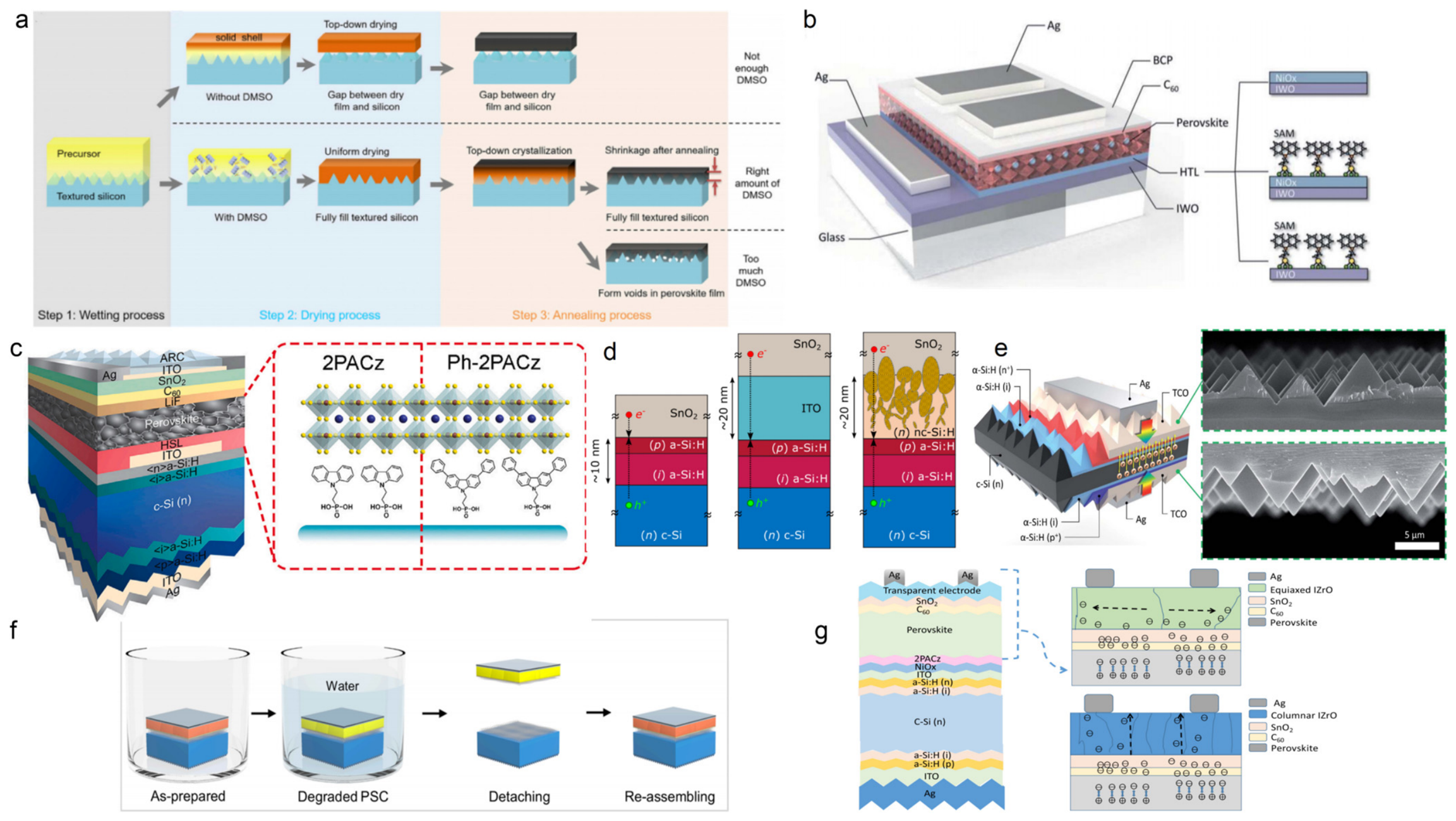
Early work by Albrecht et al. demonstrated a fully low-temperature (<120 °C) transport-layer process compatible with SHJ bottom cells, where an ALD-SnO2 ETL and a spiro-OMeTAD/MoO3/ITO HTL stack enable efficient carrier transport, yielding a stabilized efficiency of 18.1% [89]. Subsequently, Chen et al. addressed film inhomogeneity on textured silicon by employing nitrogen-assisted blade coating of PTAA, producing pinhole-free HTLs (Figure 7a) and achieving a tandem PCE of 26.2% [42]. To further improve interfacial energetics and carrier transport, composite and bilayer HTLs have been developed. Zhang et al. studied a NiOx/SAM HTL incorporating 2PACz (Figure 7b), which passivates surface defects and improves energy alignment, while Ma et al. optimized NiOx/PTAA bilayers via solvent engineering to enhance polymer ordering and hole mobility. Both strategies effectively suppress recombination and improve device performance [84,90]. More recently, molecular engineering of SAM-based HTLs has become a key direction. Ho-Baillie et al. developed Ph-2PACz with extended π-conjugation to reduce energy-level offset and improve conductivity (Figure 7c). Golobostanfard et al. demonstrated that MeO-2PACz promotes oriented perovskite growth and suppresses defect formation, both leading to reduced voltage loss and improved film quality [47,91]. In parallel, advanced HTL architectures have also been explored. Borchert et al. achieved conformal coverage on textured substrates using thermally evaporated HTLs with precise thickness control, while Shen et al. designed a dopant-free poly-TPD/spiro-TTB bilayer enabling efficient hole extraction via cascaded energy alignment, resulting in efficiencies approaching 30% [92,93].
In addition, Zhang et al. explored LiCl-doped SnO2 ETLs, in which Cl− passivates surface defects, while Li+ enhances conductivity and adjusts the conduction band position, thereby increasing Voc to 1.244 V and enabling a tandem efficiency of 25.42% [94]. Wei et al. developed two low-temperature solution modification strategies for metal-oxide ETLs to optimize interfacial energy matching and film quality. First, they proposed UV-assisted TiI4 surface augmentation for TiO2. Iodides merely chemisorb on the TiO2 surface without altering its bulk lattice, which reversibly tunes work function, uplifts conduction band, expands perovskite grains, and lifts single-junction PCE from 18.4% to 19.4%, with better repeatability [95]. Second, Saeki et al. proposed a sequential diluted spin-coating strategy to fabricate pinhole-free, ultrasmooth SnO2 films, which suppress non-radiative recombination and deliver a champion 4T tandem PCE of 22.99%. Unencapsulated devices retain 90% efficiency after 1000 h aging. Both mild-process techniques are compatible with large-area roll-to-roll tandem module manufacturing [96]. From a fabrication perspective, mitigating sputtering-induced damage has become a key consideration. Huang et al. investigated an ALD-SnO2 buffer layer to replace BCP, which improves interfacial adhesion and resists IZO sputtering damage, achieving a PCE of 26.0%. In a related approach, Du et al. introduced a highly transparent In2O3 buffer layer with favorable alignment to C60, enabling efficient electron extraction while protecting the perovskite during ITO deposition [97,98]. Beyond planar layer optimization, structural design of ETLs has also emerged as an effective route. Abbasiyan et al. investigated a partially passivated TiO2 nanorod array modified with a PMMA:PCBM blend, where the structured interface suppresses interfacial recombination and reduces series resistance. When integrated with an optimized Si3N4 antireflection layer, the four-terminal tandem device achieved an efficiency of 30.73% [99]. Overall, ETL engineering has progressed from conventional material selection toward coordinated defect passivation, interface protection, and structural design, collectively improving carrier extraction and device stability in perovskite/silicon TSCs.
The intermediate recombination layer (IRL) must enable efficient vertical carrier recombination while minimizing parasitic absorption and lateral shunting. McDonald et al. used in situ grown n-type nc-Si:H via PECVD, whose low-resistance contact with SnO2 arises from favorable band alignment, and refractive index-matching function reduces optical reflection (Figure 7d) [100]. To overcome parasitic absorption and lateral leakage in nc-Si:H, Li et al. designed nc-SiOx:H tunnel junctions, where vertically aligned nanocrystalline Si domains embedded in an amorphous matrix promote directional tunneling, while the insulating oxide matrix suppresses lateral conduction [101]. Liu et al. employed p+/n+ poly-Si junctions for perovskite/tunnel oxide passivated contact (TOPCon) TSCs. A two-step annealing prevents dopant interdiffusion, yielding an atomically steep junction that lowers contact resistivity and raises implied Voc via enhanced band-to-band tunneling [102]. Alternative IRLs exploit distinct transport mechanisms. Zhang et al. used spray-coated single-walled carbon nanotube networks (Figure 7f), where the porous architecture provides percolative conductivity and high transmittance, while the replaceable top-cell design leverages the mechanical decoupling of the junction [103]. Chozas-Barrientos et al. introduced an all-organic n-n-p molecular junction (doped C60/TaTm), whose low lateral conductivity arises from the organic matrix, effectively blocking shunting paths on textured Si, while vertical transport is maintained through molecular orbital overlap [104]. In a word, IRL design has evolved from inorganic silicon-based tunnel junctions toward diversified architectures incorporating oxide-modified, carbon-based, and fully organic RLs, aiming to balance optical transparency, electrical conductivity, and recombination efficiency in high-performance tandem devices.
Three representative interconnect/recombination systems have been widely exploited in monolithic perovskite tandem devices, exhibiting distinct trade-offs in electrical transport, optical performance, and fabrication compatibility. The nanocrystalline silicon (nc-Si:H) tunnel junction stands out with low series resistance and well-matched band structures that facilitate efficient carrier tunneling, together with mature deposition techniques compatible with industrial silicon manufacturing. Nevertheless, this architecture suffers from unavoidable parasitic light absorption across visible and near-infrared spectra, and lateral shunting defects tend to emerge when deposited on textured silicon wafers, deteriorating device fill factors. As an alternative, ultrathin ITO interlayers deliver outstanding full-spectrum optical transmittance and can be readily fabricated via magnetron sputtering, yet high-energy sputtering particles would inflict irreversible structural damage to the underlying perovskite absorber layers, accompanied by moderately high contact resistance that aggravates voltage loss. Differing from inorganic tunneling materials, conductive SAM-based all-organic molecular junctions completely eliminate parasitic optical absorption and enable damage-free low-temperature solution deposition, which efficiently restrains lateral leakage paths. Unfortunately, such organic interconnects are restricted by insufficient vertical carrier conductivity, and their molecular frameworks tend to decompose under prolonged thermal and illumination stress, resulting in unsatisfactory long-term operational stability.
For transparent electrodes, the core challenge is balancing free-carrier absorption and sheet resistance. Zheng et al. replaced ITO with W-doped In2O3 (IWO). The large valence difference between W6+ and In3+ allows low resistivity at reduced carrier density, cutting near-infrared (NIR) parasitic absorption from 12.4% to 0.6% (Figure 7e) [105]. In addition, the optimization of transparent conductive oxides has focused on deposition process control. The Sittinger team studied sputtering parameter engineering (substrate temperature, oxygen partial pressure, and target power) to improve ITO and IZO films, achieving a carrier mobility of 50 cm2/V·s and a weighted absorption below 3.1%, which enabled tandem efficiencies of 24.3% [106]. Similarly, Kabaklı et al. studied oxygen flow-controlled DC sputtering to fabricate low-defect ITO films with a mobility of 53.4 cm2/V·s. By constructing a bilayer ITO with different oxygen contents, the interfacial barrier with SnOx was reduced, increasing the average tandem efficiency from 22% to 25% [107]. Wang et al. tuned IZO thickness to modulate optical interference within the perovskite, thereby adjusting sub-cell photocurrent balance via cavity effects [108]. Hatt et al. used ALD-Al2O3 as a protective mask during electroplated Cu metallization, ensuring chemical stability for large-area processing [109]. Finally, Zhang et al. designed bilayer IZrO with a columnar-equiaxed dual microstructure. The columnar phase enhances vertical transport, the equiaxed phase improves lateral spreading, and the graded refractive index minimizes reflection, achieving certified 30.12% PCE (Figure 7g) [110].
In general, IRL design has shifted from simple inorganic tunnel diodes toward oxide-modified, carbon-based, and organic junctions, each exploiting distinct carrier-transport and leakage-suppression mechanisms. Transparent electrodes have evolved from conductivity-transparency trade-offs to integrated optical–electrical–structural engineering, enabling better current matching, reduced losses, and scalable high-performance TSCs. Table 5 summarizes the transport-layer strategies and the photovoltaic parameters of perovskite/silicon TSCs. nc-Si tunnel junctions offer high conductivity but cause optical loss. All-organic interconnects reduce parasitic absorption but suffer from poor heat resistance. Composite oxide transport layers strike the best balance of optical and electrical performance. Perovskite/silicon systems benefit most from lattice rigidification and SAM passivation due to inert silicon substrates. This set of strategies cannot be fully replicated in flexible thin-film tandem architectures.
Table 5.
Transport-layer strategies and the PV parameters of perovskite/silicon TSCs.
Figure 7.
(a) Schematic depiction of the evolution of a perovskite layer on a textured surface. Reprint with permission [42]. Copyright 2020, Elsevier. (b) Schematic diagram of an inverted planar PSC. Reprint with permission [84]. Copyright 2022, Royal Society of Chemistry. (c) Schematic of the p-i-n silicon–perovskite TSC. Reprint with permission [91]. Copyright 2023, Elsevier. (d) Device performance of perovskite–Si TSCs with various RJs. Reprint with permission [100]. Copyright 2022, American Chemical Society. (e) Schematic diagram and the FESEM images of the bifacial HIT silicon solar cell. Reprint with permission [105]. Copyright 2019, Royal Society of Chemistry. (f) The detachment and reassembly of 2-T perovskite/Si tandem via the accelerated aging procedure. Reprint with permission [103]. Copyright 2024, American Chemical Society. (g) Structure and carrier transport path schematic of a perovskite/Si TSC. Reprint with permission [110]. Copyright 2025, American Chemical Society.
3.2. Perovskite/CIGS TSCs
Perovskite/CIGS TSCs are another promising architecture that combines the high efficiency of CIGS solar cells with the tunable bandgap and low-cost fabrication of perovskite materials. In this architecture, a WBG perovskite top cell is stacked on top of an NBG CIGS bottom cell. The CIGS bottom cell, which is known for its high PCEs and excellent stability, provides a reliable base for the tandem cell, while the perovskite top cell allows for the absorption of high-energy photons that are not efficiently captured by the CIGS cell. Similar to perovskite/silicon TSCs, perovskite/CIGS TSCs can be fabricated in both monolithic and mechanically stacked configurations. Monolithic perovskite/CIGS tandem cells offer the advantage of a more efficient charge transfer between the two sub-cells, but the fabrication process is more complex and requires precise control over the growth and interface properties of the two materials. Mechanically stacked perovskite/CIGS TSCs, on the other hand, offer greater flexibility in terms of material selection and device design, but the mechanical-stacking process can introduce additional optical and electrical losses.
3.2.1. Perovskite-Layer Regulation
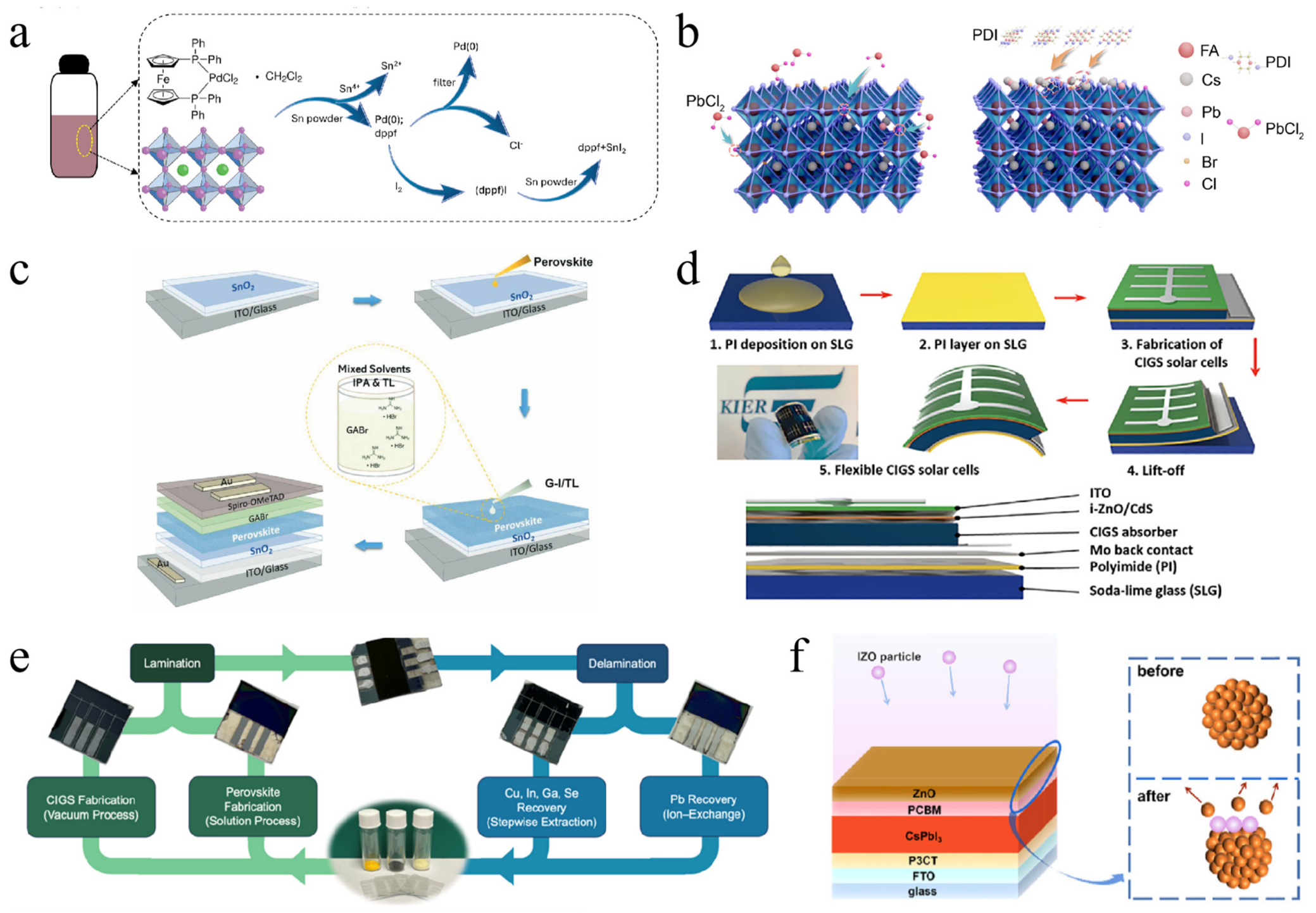
Surface defects and composition mismatch are the core issues limiting the performance of perovskite/CIGS TSCs. To address these problems, strategies such as organic salt modification, ion doping, and additive regulation have been developed, which can precisely passivate defect sites while optimizing the crystal structure and band alignment of perovskites. Energy-band alignment at interfaces is achieved by selecting transport layers (Cu:NiOx for hole extraction, and bis-C60 for electron barrier reduction) and adjusting the CIGS composition (increasing S/Se ratio raises CIGS conduction band to reduce the CdS barrier) [111]. In p-i-n structures, MDADI supplies I− to fill iodine vacancies and coordinate uncoordinated Pb2+, suppressing non-radiative recombination [112]. FABr treatment induces synchronous FA+/Br− diffusion. FA+ adjusts the tolerance factor to stabilize the cubic phase, while Br−/Cl− exchange passivates halogen vacancies and removes secondary phases [113]. In CsFAPb(IBr)3, Cl doping combined with PDI surface treatment increases ion-migration activation energy and reduces phase/surface defects (Figure 8b) [114]. For lead-free tin perovskites, the Pd(dppf)Cl2 additive acts multifunctionally. The benzene ring delays crystallization via weak interactions, Cl− coordinates uncoordinated Sn2+, and Fe2+/Pd2+ synergistically reduces Sn4+ to Sn2+, inhibiting oxidation (Figure 8a) [115]. The preparation process of perovskite films directly affects their crystallization quality and coverage uniformity. Especially for the irregular and rough surface of CIGS bottom cells, process innovation is required to achieve conformal deposition and defect control, while balancing large-area compatibility and high performance. Ultrasonic spray coating disperses precursor into micron droplets for conformal deposition, while SAMs and LiF/C60/BCP layers passivate interfaces [116]. Stepwise DMSO annealing first applies 100 °C to break precursor-DMSO coordination for rapid nucleation and large grains, and then 80 °C to slowly release residual solvent, avoiding pinholes and suppressing volatile-halide sublimation that forms PbI2 impurities [117].
In addition, with the aid of numerical simulation tools and multi-junction structure design, the band alignment, thickness parameters, and charge-transport paths of perovskite/CIGS TSCs can be systematically optimized. This maximizes light absorption and carrier-utilization efficiency, breaking through the limitations of experimental optimization. Multi-junction designs exploit complementary absorption bands (400–800 nm vs. 800–1200 nm) and concentration effects (linear Jsc increase; logarithmic Voc rise) to reduce thermal and series-resistance losses [118]. On the other hand, a study employed SCAPS-1D numerical simulation to optimize a monolithic 2-terminal 2D-3D perovskite/CIGS TSC. Ultimately, the top cell achieved a PCE of 21.41%, the bottom cell had a PCE of 12.98%, and the tandem cell PCE exceeded 30%. The study optimized the top cell by adjusting the perovskite bandgap and thickness. Increasing the bandgap enhanced the quasi-Fermi level difference, and increasing the thickness improved light absorption. For the bottom cell, the study optimized the thickness of p-CIGS and n-GaSe to enhance long-wave light absorption and reduce interface defects, and controlled the doping concentration to optimize charge transport [119]. In addition, Y. K. Singh et al. first determined Cu2O as the optimal HTL and ZnO as the optimal ETL, thereby optimizing the charge-transport path and reducing the transmission obstacles. Subsequently, they optimized the thickness of the active layer (1 μm for the top battery, and 3 μm for the bottom battery) and the defect density (1 × 1010 cm−3 for the top cell body defect density, and 1 × 1014 cm−3 for the bottom cell), thereby reducing the non-radiative recombination of charge carriers. Then, they combined with filtering spectroscopy analysis and current-matching adjustment to avoid current loss. The combined effect of these three factors significantly improved the performance of the tandem battery, ultimately achieving a PCE of 34.52%, Voc of 2.29 V, Jsc of 17.59 mA/cm2, and FF of 85.69% [120]. Table 6 summarizes the defect modification and component regulation strategies and the photovoltaic performance of the corresponding perovskite/CIGS TSCs. For CIGS bottom cells, mild halide tuning avoids lattice mismatch damage. Spray coating conformal perovskite films works better than spin coating on rough CIGS surfaces for flexible devices.
Table 6.
Defect modification and component regulation strategies and the PV performance of the corresponding perovskite/CIGS TSCs.
3.2.2. Interface Regulation
Interface defects and energy-level mismatch are the core bottlenecks restricting the carrier transport efficiency of perovskite/CIGS TSCs. Some research teams have achieved the synergistic optimization of defect passivation, energy-level alignment, and crystallization quality improvement through strategies such as organic molecule modification and dopant regulation. GABr in an IPA–toluene mixed solvent reduces IPA erosion while enabling GA+–iodine coordination and Br− filling of halogen vacancies. It also promotes α-phase crystallization and optimizes energy alignment (Figure 8c) [121]. The Me-4PACz self-assembled monolayer conforms to rough CIGS, while PEAI forms a 2D/3D heterojunction that passivates surface traps. LiF acts as a dipole layer to lower the C60/perovskite barrier, and RbF post-treatment increases Cu-vacancy density, enhancing p-type conductivity [122]. On NiOx, 4PADCB binds via phosphonic acid, reducing the Ni3+/Ni2+ ratio, adjusting valence-band position for hole extraction, and improving wettability for conformal perovskite growth [123]. Intermediate layers serve as both chemical barriers and transport bridges. A 20 nm IZO layer between AZO and perovskite blocks deprotonation reactions (AZO alkaline sites vs. MA+ cations) and inhibits Zn2+/I− interdiffusion, while its conduction band (~−4.5 eV) ensures efficient electron transfer; it also induces oriented perovskite crystallization [124]. In addition, the interfacial stability and mechanical properties of flexible perovskite/CIGS TSCs are highly dependent on substrate modification and CIGS-layer growth regulation. Synergistic breakthroughs in the efficiency and stability of flexible devices can be achieved through PI substrate modification, gradient composition design of the CIGS layer, and doping optimization. On PI, a graded Ga profile and trace Ag seeding improve CIGS quality [125]. Alternatively, a PI interlayer on SLG suppresses Na+/K+ diffusion via steric/chemical adsorption, preventing K+ substitution for VCu, and matches thermal expansion to shift the neutral plane, reducing bending stress (Figure 8d) [126]. Interface regulation involves molecular scale passivation chemistry, dipolar energy-level modulation, diffusion-blocking interlayers, and stress-managed substrate design. All of these strategies aim to reduce non-radiative recombination, improve band alignment, and enhance mechanical integrity. Table 7 summarizes the interface modulation and interlayer design strategies and the photovoltaic performance of the corresponding perovskite/CIGS TSCs. Buffer interlayers block ion interdiffusion between perovskite and CIGS, outperforming single-molecule passivation alone. SAM modification fits uneven CIGS substrates most effectively.
Table 7.
Interface modulation and interlayer design strategies and the PV performance of the corresponding perovskite/CIGS TSCs.
3.2.3. Transport-Layer Strategies
The material selection of transport layers and buffer layers directly affects carrier transport efficiency and device stability. Some research teams have addressed core issues such as ion diffusion, parasitic absorption, and process damage through strategies including replacing traditional materials, removing redundant layers, and constructing protective buffer layers. During ITO sputtering, high-energy Ar+ ions oxidize amino groups of spiro-OMeTAD to C=O bonds, reducing the energy offset at the spiro-OMeTAD/ITO interface and eliminating the hole injection barrier. Removing the MoOx buffer layer avoids near-infrared parasitic absorption and interface defects from its thermal decomposition, while K doping fills lattice vacancies and suppresses I− migration, improving crystallinity and transport [127]. A ZnO nanoparticle buffer layer deposited by a water-free spin-coating process disperses Ar+ impact during IZO sputtering, blocks In diffusion into the perovskite, and prevents the CsPbI3 phase transition caused by water. DMAI in the precursor regulates crystallization, enlarging grains and reducing defect density, while P3CT and PCBM align with the valence and conduction bands to lower the charge-extraction barrier (Figure 8f) [128]. Numerical simulations enable precise screening of transport layers and interface structures. A 1 nm Me-4PACz layer passivates perovskite surface defects through its phosphonic acid groups, and its HOMO matches the perovskite valence band to enhance hole extraction and reduce parasitic absorption. The Me-4PACz/ITO tunnel recombination junction provides efficient recombination and low-resistance transport between sub-cells [129]. In an HTL-free architecture with BaSnO3 as the ETL, a favorable conduction band offset with the perovskite suppresses electron backflow and promotes extraction, while the high electron mobility of BaSnO3 reduces series resistance. The absence of NiO removes the associated interface barrier. The triple-cation perovskite further improves stability by suppressing phase separation [130]. For damage-free integration via lamination, a transparent conductive adhesive (TCA) exploits Al2O3 nanoparticles to disrupt PVDF-HFP crystalline domains, creating more transport channels for the ionic liquid. Hydrogen bonds between PVDF-HFP C-F groups and ITO hydroxyls, together with EMI+ binding to oxygen vacancies on ITO, ensure strong adhesion. Low-temperature (80 °C) dry transfer prevents thermal degradation and solvent erosion of the perovskite, and the weak TCA–perovskite interaction eliminates lead residue during peeling (Figure 8e) [131]. Low-temperature organic transport materials match flexible CIGS fabrication, while metal oxide layers deliver higher charge mobility but require high-temperature treatment incompatible with plastic substrates. CIGS-based TSCs prioritize conformal deposition and stress-relief interlayers, restricted by rough surfaces and flexible substrate limits. High-temperature lattice engineering is less effective here.
Figure 8.
(a) Schematic diagram of possible chemical reactions in solution. Reproduced with permission [115]. Copyright 2025, American Chemical Society. (b) Schematic diagram of the Cl bulk incorporation and PDI surface treatment. Reproduced with permission [114]. Copyright 2023, Royal Society of Chemistry. (c) Schematic fabrication process of a planar PSC. Reproduced with permission [121]. Copyright 2022, Wiley-VCH GmbH. (d) Lift-off process for f-CSCs. Reproduced with permission [126]. Copyright 2024, Elsevier. (e) Circular loop of laminated perovskite–CIGS PSC. Reproduced with permission [131]. Copyright 2024, American Chemical Society. (f) Impact of buffer-layer deposition. Reproduced with permission [128]. Copyright 2024, Elsevier.
3.3. All-Perovskite TSCs
All-perovskite TSCs are a relatively new and exciting architecture that uses two different perovskite materials with different bandgaps to form a tandem cell. In this architecture, a WBG perovskite top cell is stacked on top of an NBG perovskite bottom cell. The advantage of all-perovskite tandem cells is that they can be fabricated using a single material system, which simplifies the fabrication process and potentially reduces costs. Additionally, the tunability of the bandgap of perovskite materials allows for precise optimization of the optical absorption characteristics of the two sub-cells to maximize the efficiency of the tandem cell. However, the development of all-perovskite TSCs also faces several challenges. One of the main challenges is the instability of perovskite materials, especially under high humidity, temperature, and light-exposure conditions. To address this issue, various strategies have been proposed, such as the use of stable perovskite compositions, the incorporation of protective layers, and the optimization of the device architecture. Another challenge is the development of efficient and stable RLs for all-perovskite TSCs, as the interface between the two perovskite materials can introduce significant recombination losses.
3.3.1. Perovskite-Layer Regulation
Mechanisms for suppressing Voc loss and photoinduced halide segregation in WBG perovskites center on defect passivation, ion-immobilization, and energy-level tuning. DMA induces octahedral tilting through steric hindrance, shortening Pb-I bonds and raising the VBM to widen the bandgap and hinder halide migration, while Cl− fills iodine vacancies and lowers the CBM [132]. PbCl2 supplies Cl− to form a trihalide phase that reduces halide vacancies and inhibits migration, while PMACl forms a surface 2D perovskite that passivates defects and blocks moisture [133]. PDA uses bidentate coordination to uncoordinated Pb2+ and hydrogen bonds to fill halide vacancies, optimizing energy alignment with C60, strengthening the built-in field, and suppressing PbI2/Br-rich phase separation [134]. DBSA coordinates Pb2+ via its sulfonate group, and the long alkyl chain sterically restricts grain tilting to guide (001) vertical growth. Its oxygen atoms form Pb-O and H-bonds with FA+, passivating bulk defects and homogenizing the surface electric field to suppress I/Br phase segregation (Figure 9d) [135]. DDPA employs phosphonic acid groups to strongly coordinate with FA+, halides, and uncoordinated Pb2+, suppressing VFA, VI, and VPb, while the alkyl chain restricts tilting and promotes (011) orientation, and its hydrophobicity enhances moisture resistance [136]. F-PEAI spin coating forms a 2D FPEA2PbI4 capping layer concentrated in the top 10 nm. The large organic cations increase the activation energy for halide migration, inhibit I/Br phase separation, passivate grain-boundary/surface defects, and enhance the built-in potential without introducing a transport barrier (Figure 9a) [137]. Piracetam preferentially adsorbs on the (110) plane to induce oriented growth, then reacts with residual PbI2 to form 1D nanoneedles and hydrogen-bonds with FA+ to suppress vacancy defects (Figure 11a) [138]. Furthermore, Du et al. added 2,5-dibromothieno [3,2-B]thiophene (DBrT) as an additive to the perovskite precursor of FA0.75Cs0.25PbI2.4Br0.6. For the inverted WBG PSCs, the PCE reached 22.40%. The semi-transparent WBG device achieved a PCE of 20.39%. And the four-terminal tandem device broke through a PCE of 28.31%. This is because after crystallization, DBrT diffuses to the grain boundaries as well as the upper and lower surfaces of the perovskite. It passivates the uncoordinated Pb2+ defects, inhibits the phase separation of iodine/bromine, optimizes the energy-level alignment between the perovskite and C60, and prolongs the carrier lifetime simultaneously (Figure 9c) [139].
On the other hand, Fu et al. proposed an in situ molecular compensation optimization method by introducing 5-aminovaleric acid hydroiodide (5-AVAI) into the 1.79 eV WBG perovskite precursor. By adding 5-AVAI to the precursor of WBG perovskite (Cs0.2FA0.8Pb(I0.6Br0.4)3), the single-junction WBG PSCs achieved a champion PCE of 20.23%. After integrating with an NBG bottom cell (PCE 22.01%), the champion PCE of the all-perovskite TSCs (APTSCs) reached 28.9%. Owing to its high dipole moment (2.57 Debye, higher than 1.60 Debye of Me-4PACz) and small horizontal diameter (3 Å), 5-AVAI migrates spontaneously to the buried interface during perovskite deposition. It compensates for the defect sites of SAMs through strong coordination and hydrogen bonding, reducing interfacial energy loss. Meanwhile, its amphoteric property, possessing both amino and carboxyl groups, enables interaction with the perovskite lattice via hydrogen bonding, passivating grain boundary defects, inhibiting ion migration caused by VI and VCs/VFA, and alleviating halide segregation (Figure 10a). Additionally, 5-AVAI can regulate perovskite crystallization, improve film compactness, extend carrier lifetime, and reduce non-radiative recombination [140]. p-OHPEAI adsorbs parallelly via synergistic -NH3+ and -OH, avoiding an insulating 2D phase. -NH3+ binds uncoordinated Pb2+ and I− fills Pb vacancies, while -OH increases the electron density on the benzene ring to suppress metallic Pb and forms a dipole layer at the perovskite/C60 interface to accelerate carrier extraction [141].
Figure 9.
(a) The schematic illustration of 2D wrapped 3D structural perovskite. Reproduced with permission [137]. Copyright 2024, American Chemical Society. (b) Schematics illustrating membrane filtration and magnetic filtration processes. Reproduced with permission [142]. Copyright 2024, Wiley-VCH GmbH. (c) Schematic diagram of adding DBrT in the growth process of perovskite crystals. Reproduced with permission [139]. Copyright 2024, Wiley-VCH GmbH. (d) Schematic diagrams of a possible (001) facet-stacking mode. Reproduced with permission [135]. Copyright 2023, Wiley-VCH GmbH. (e) Schematic illustration of the operational mechanism for TFPHCl-induced self-assembly. Reproduced with permission [143]. Copyright 2024, Royal Society of Chemistry. (f) Schematic evolution of perovskite films. Reproduced with permission [144]. Copyright 2025, Royal Society of Chemistry.
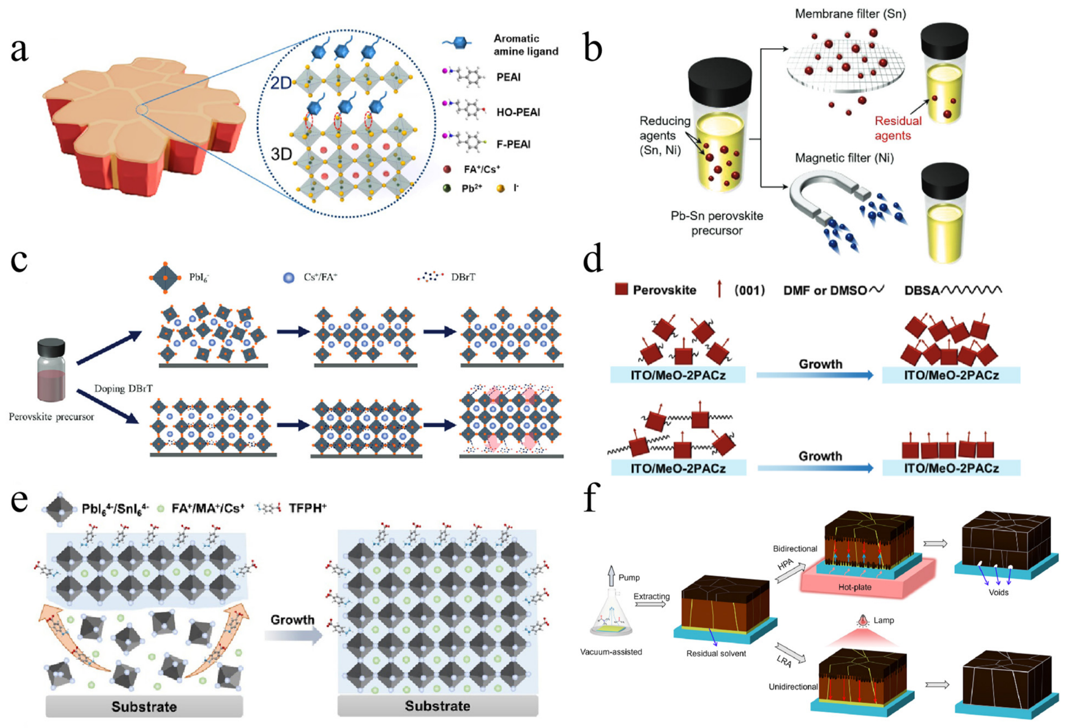
NBG Pb-Sn perovskites are essential for bottom cells in TSCs but suffer from poor vertical uniformity, easy oxidation of Sn2+, and severe interfacial recombination. Xing et al. employed a molecular anchoring strategy using L-alanine methyl ester (AME) as additive, a PEA2PbI3SCN buried layer, and EDA(I/Cl)2 post-treatment to prepare vertically uniform Cs0.1MA0.3FA0.6Pb0.5Sn0.5I3 films with optimized interfaces, achieving a champion single-junction PCE of 22.3% and a 4-T all-perovskite tandem PCE of 27.1% [145]. Sun et al. introduced benzyl viologen (BV) for surface charge-transfer doping, which shifted the Fermi level upward by 0.29 eV, suppressed Sn2+ oxidation, and strengthened the built-in field, yielding single-junction PCE of 22.58% and 2-T tandem PCE of 26.33% [146]. 4-Trifluoromethylphenylhydrazine hydrochloride (TFPHCl) was added into a FA0.7MA0.3Sn0.5Pb0.5I3 precursor. The TFPH+ cations floated to the surface and formed an antioxidant p/p− homojunction that improved stability and charge separation (Figure 9e), resulting in single-junction PCE of 23.09% and tandem PCE of 27.42% [143]. Introducing canolol (CNL), a natural reactive-oxygen-species scavenger, into a (FASnI3)0.6(MAPbI3)0.4 precursor balanced crystallization reduced defects, and extended carrier lifetime. The champion single-junction PCE reached 23.7% (22.08% for 1.035 cm2), and the 2-T tandem PCE attained 28.71% (27.2% for large area) [147]. Succinic acid (AA) and thiomalic acid (TA) were used as additives. AA strengthens Sn-I bonds and suppresses iodine migration (single-junction PCE 21.95%), while TA adds reductive thiol groups that directly reduce Sn4+ and relieve tensile strain (single-junction PCE 22.7%). A TA-modified bottom cell enabled a 2-T tandem PCE of 28.6% [148]. Replacing Sn particles with Ni particles as the reducing agent (Figure 9b) takes advantage of the lower reduction potential of Ni and its ferromagnetism for magnetic removal, yielding single-junction PCE of 22.29% and a monolithic tandem PCE of 28.13% [142]. Zhao’s team introduced K2SnO3 into the precursor and PEDOT:PSS, in situ generating PbSnO3 seeds that induce vertical grain growth and synergistically passivate defects (Figure 10c). Single-junction NBG PCE reached 23.12%, 2-T tandem 28.12%, and 4-T tandem 28.81% [149].
Wang et al. developed a confined-space annealing (CSA) strategy that slows solvent release to improve crystallinity and reduce defects (Figure 10d), achieving NBG single-junction PCE of 21.51% and tandem PCEs of 25.15% (4-T) and 25.05% (2-T) [150]. In situ growth of a BABr quasi-2D layer on CsPbI2Br formed a 2D/3D heterostructure that passivates defects and enhances hole extraction (Figure 10b), giving a single-junction PCE of 16.57% and a monolithic tandem PCE of 10.22% [151]. Another study proposed an optimization method for photonic radiative annealing, which regulates crystal growth through rapid top-down heating and has been applied to all-perovskite TSCs. In traditional vacuum-assisted processes, the strong solvent extraction at the interface between the wet film and the vacuum leads to the formation of a thin perovskite layer on the top surface and residual solvents at the buried interface, ultimately causing film delamination and voids. However, the rapid top-down heating of photonic radiative annealing can precisely control the solvent evaporation rate, avoid uneven solvent distribution at the interface, and guide the unidirectional growth of crystals. As a result, high-quality Sn-Pb perovskite films with more uniform composition, fewer grain boundary defects, no obvious delamination, and no buried voids are obtained, reducing bulk and interfacial non-radiative recombination (Figure 9f). The performance of the optimized devices has achieved a significant breakthrough. The single-junction vacuum-assisted Sn-Pb perovskite solar cell has achieved a PCE of 22.31%, and the efficiency of the all-perovskite TSC has been further increased to 27.62% [144]. Table 8 summarizes the WBG and NBG perovskite optimization strategies and the photovoltaic performance of corresponding all-perovskite TSCs. WBG triple-halide passivation restrains I/Br segregation. Sn-Pb NBG antioxidant additives are mandatory. Dual bulk-surface treatment simultaneously lifts the performance of both sub-cells.
Table 8.
WBG and NBG perovskite optimization strategies and the PV performance of corresponding all-perovskite TSCs.
Figure 10.
(a) Molecule structures and schematic of interface compensation. Reproduced with permission [140]. Copyright 2025, The Royal Society of Chemistry. (b) Schematic diagram of the preparation process and 2D/3D heterostructure of CsPbI2Br solar cells. Reproduced with permission [151]. Copyright 2022, The Royal Society of Chemistry. (c) Schematic diagram illustrating the seed-induced oriented crystallization of K2SnO3-treated perovskite films. Reproduced with permission [149]. Copyright 2025, Springer Nature. (d) Scheme of normal annealing, solvent annealing and CSA processes. Reproduced with permission [150]. Copyright 2022, Springer Nature. (e) Schematic diagram of defect passivation and dipole moment generated by GABr/F-PEAI. Reproduced with permission [152]. Copyright 2024, Elsevier.
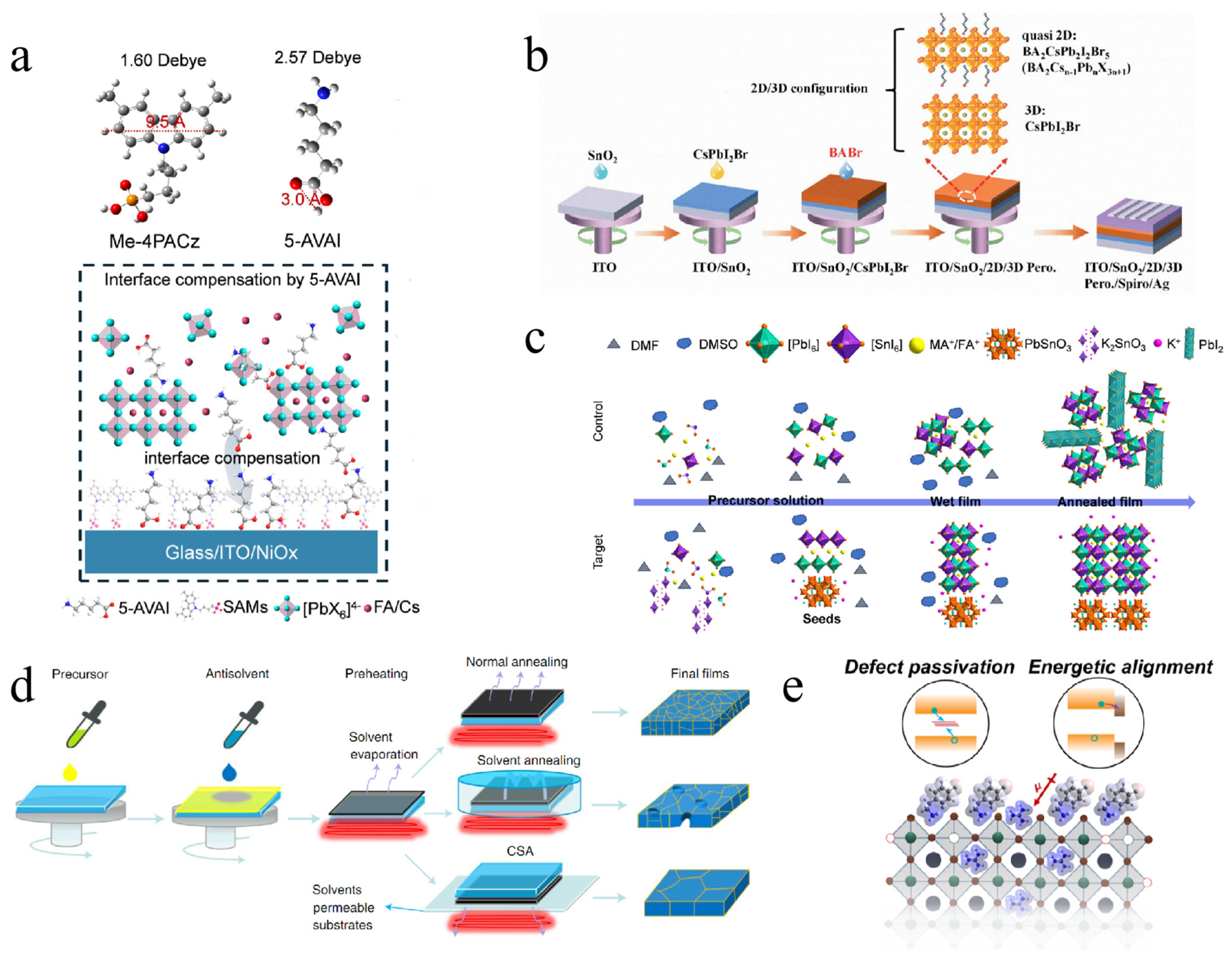
3.3.2. Interface Regulation
WBG I/Br mixed perovskites suffer from abundant interfacial defects, poor crystallinity, and photoinduced halide segregation. Various interfacial modification strategies have been developed to simultaneously passivate defects, align energy levels, and suppress ion migration. A four-source vacuum deposition technique produced FA0.7Cs0.3Pb(IxBr1−x)3 films with precise bandgap control (1.62–1.80 eV). Combining MeO-2PACz as HTM and EDAI2 surface passivation yielded a 2-T all-perovskite tandem PCE of 24.1% [153]. Zhou et al. adopted a synergistic bulk (MASCN) and surface (PEAI) passivation for 1.71 eV WBG perovskite made by blade coating with vacuum quenching. Together with a metal-free ALD-SnO2 RL (93% transmittance, Figure 11b), the tandem device achieved 23.65% PCE [154]. Zhang et al. employed binary cations GABr and F-PEAI together with Al2O3 nanoparticles to improve wettability and passivate the WBG perovskite. The 1.80 eV WBG cell reached 19.0% PCE and the tandem device 27.2% PCE (Figure 10e) [152]. Chen et al. inserted 6-hydroxy-2-naphthalenecarboxylic acid (HNA) at the WBG/C60 interface, building a cross-linked conjugated network that passivates defects and accelerates charge extraction, leading to a tandem PCE of 28.25% [155]. Modifying the buried HTL/perovskite interface with the silane coupling agent CN-TMOS gave a 1.77 eV WBG cell with 19.69% PCE and a tandem PCE of 28.45% [156]. Guo et al. used PACl at the SnO2/perovskite buried interface to stabilize 1.68 eV MAPbI2.4Br0.6 through low-dimensional perovskite formation, relieving strain and suppressing halide segregation. The 4-T tandem reached 27.21% PCE [157]. A dual-molecule approach with BzMIMBr additive and DMFP surface passivation formed an A-B-A sandwich structure, yielding a WBG PCE of 22.77% and a 4-T tandem PCE of 26.18% [158].
For NBG Pb-Sn perovskites, interface strategies target severe non-radiative recombination, high carrier barriers, and Sn2+ oxidation. Sun et al. constructed an internal self-anchored dual-passivation (ISADP) layer by spin coating EDAI2, followed by PCBM. The synergistic effect boosted the NBG cell PCE to 24.02% and the monolithic tandem to a certified 28.12% (28.61% champion) [159]. Song et al. modified the PEDOT:PSS/Pb-Sn perovskite interface with ammonium sulfide (AS), generating PbS nucleation sites, reducing acidity, and optimizing the energy landscape, achieving a single-junction PCE of 24.23% and a tandem PCE of 27.48% [160]. Benzyl viologen (BV) was introduced for surface charge transfer doping during the perovskite spin-coating process via anti-solvent engineering, utilizing the electron-donor property of BV to compensate for excess holes on the perovskite surface. BV molecules have an extremely low reduction potential, enabling them to transfer electrons to the perovskite surface and compensate for excess holes, converting the perovskite from heavily p-type doped to lightly p-type. BV forms coordination interactions with uncoordinated Sn2+ on the perovskite surface, inhibiting the oxidation of Sn2+ to Sn4+ and reducing Sn vacancy defects. Additionally, BV optimizes the energy-level alignment at the perovskite/C60 interface, enhances the interfacial built-in electric field, and accelerates carrier extraction. Benefiting from these effects, the champion PCE of the single-junction NBG PSCs reached 22.58%. The champion PCE of the all-perovskite tandem device reached 26.33% [146]. Table 9 summarizes the interface modification strategies for WBG and NBG perovskites and the photovoltaic performance of the corresponding all-perovskite TSCs. 2D/3D heterojunctions suppress WBG interfacial loss, while reductive interface layers mitigate Sn2+ oxidation in NBG perovskites. Combined dual-side passivation gains the highest tandem Voc.
Table 9.
Interface modification strategies for WBG and NBG perovskites and the PV performance of the corresponding all-perovskite TSCs.
3.3.3. Transport-Layer Strategies
Traditional transport layers (e.g., PEDOT:PSS and PTAA) suffer from issues such as acid corrosion, strong parasitic absorption, and poor stability. Thus, strategies including the development of novel molecular transport layers and polymer modification can be adopted to upgrade the performance of transport layers while optimizing the interfacial compatibility with perovskites. Jiang et al. developed a novel solution-processed charge-recombination layer (CRL) with the architecture spiro-OMeTAD/PEDOT:PSS/PEI/PCBM:PEI, fabricated entirely via orthogonal-solvent low-temperature processing. Chlorobenzene served as the solvent for spiro-OMeTAD and PCBM:PEI, isopropanol for PEI, and the PEDOT:PSS layer was dry-transferred to prevent perovskite damage from aqueous solutions. The bottom perovskite sub-cell (with an Ag electrode) achieved a PCE of 11.7%, the top perovskite sub-cell (also with an Ag electrode) reached 11.4%, and the tandem device delivered a Voc of 1.89 V. In this design, spiro-OMeTAD functions as the hole-collecting layer and PCBM:PEI as the electron-collecting layer. PEI modifies the PEDOT:PSS surface to establish a work-function gradient that creates efficient charge-recombination sites, while the phase separation between PEI and PCBM enhances electron transport. Moreover, the low-temperature process eliminates thermal damage to the bottom device (Figure 11e) [161]. Bi et al. introduced the single-molecule HTL 4dp3PACz, achieving a 1.77 eV WBG cell PCE of 17.17% and a tandem PCE of 26.47% [162]. PEDOT:PSS was replaced with Pb-doped P3CT (P3CT-Pb). Its high-pKa carboxyl groups suppress deprotonation and inhibit acid erosion and iodine volatilization, and the Pb doping optimizes energy alignment and provides nucleation sites, giving an NBG cell PCE of 22.7% and a tandem PCE of 27.8% [163]. Replacing the Au layer with graphene oxide (GO) and PEDOT:PSS with 2PACz forms an SnO2/GO/2PACz interconnect that reduces parasitic absorption, avoids acidic degradation, and improves stability, delivering a tandem PCE of 23.3% [164].
The interface matching and light transmittance between electrodes and transport layers directly affect the light absorption and charge-transport efficiency of TSCs. Strategies such as electrode material replacement, buffer-layer design, and HTL-free structure construction can be adopted to achieve the synergistic improvement of optical and electrical properties. Zhao et al. employed a 4-T mechanically stacked configuration with a semi-transparent 1.75 eV WBG top cell and a 1.25 eV LBG bottom cell, using MoOx/ITO electrodes to minimize parasitic absorption, and achieved 23.1% [165]. In NBG (1.26 eV) Sn-Pb mixed PSCs, traditional HTLs suffer from parasitic absorption and significant NIR light loss in transparent electrodes. An HTL-free structure with hydrogen-doped indium oxide (IO:H) electrodes eliminated HTL parasitic absorption and enhanced near-infrared transmittance, yielding a 4-T tandem PCE of 24.8% [166]. To protect the C60 and perovskite layers during ITO sputtering, Dong et al. spin-coated a PEI buffer layer, forming a C60/PEI/ITO structure that converts into a conductive coordination compound, reduces damage, and optimizes energy alignment (Figure 11d), resulting in a 4-T tandem PCE of 26.89% [167]. Hu et al. developed a lamination process using a transparent conductive adhesive (TCA) with Ag-coated PMMA microspheres as the recombination junction, enabling independent sub-cell fabrication and self-encapsulation (Figure 11c), achieving a 2-T tandem PCE of 18.2% [168]. SCAPS-1D simulations for all-lead-free CsGeI3/FASnI3 tandem cells, with optimized transport-layer parameters and absorber thicknesses, predicted a theoretical PCE of 30.42% [169]. Table 10 summarizes the transport-layer, electrode, and interconnect-layer optimization strategies and the photovoltaic performance of the corresponding perovskite TSCs. Metal-free organic RLs avoid optical loss for all-perovskite stacks, while inorganic tunneling layers offer higher conductivity but risk damaging the underlying NBG film. All-perovskite devices require dual optimization of WBG segregation and NBG Sn oxidation, making composite passivation indispensable, while single-sided modification only brings limited efficiency gains.
Table 10.
Transport-layer, electrode, and interconnect-layer optimization strategies and the PV performance of the corresponding perovskite TSCs.
Figure 11.
(a) Schematic diagram of the growth process of WBG perovskite films. Reproduced with permission [138]. Copyright 2025, Springer Nature. (b) Schematic diagram of the vacuum-assisted blade coating. Reproduced with permission [154]. Copyright 2022, American Chemical Society. (c) Schematic of the fabrication process of the laminated architecture. Reproduced with permission [168]. Copyright 2025, American Chemical Society. (d) Optimized configuration of ITO capped on PEI fragment. Reproduced with permission [167]. Copyright 2024, Wiley-VCH GmbH. (e) Schematic of the as-prepared two-terminal bottom-up perovskite/perovskite TSC and chemical structures of the spiro-OMeTAD, PEDOT:PSS, PEI, and PCBM comprising the charge-recombination layer. Reproduced with permission [161]. Copyright 2016, The Royal Society of Chemistry.
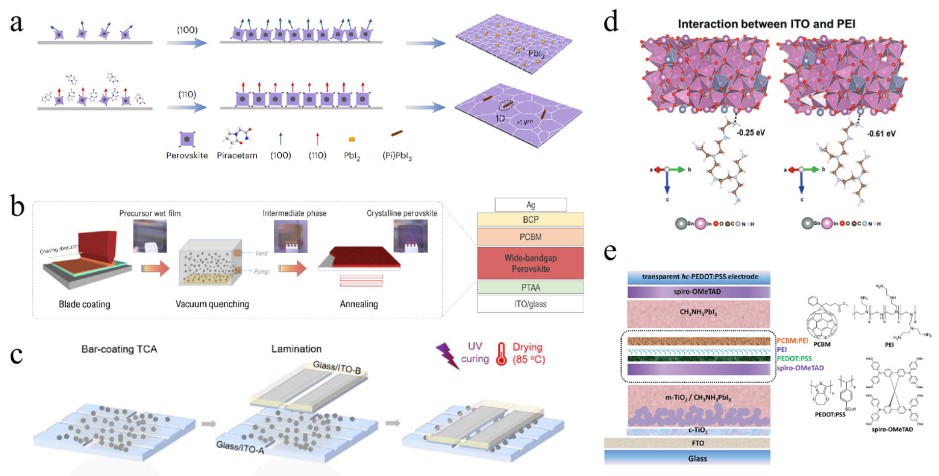
3.4. Perovskite/Organic Solar Cell (OSC) TSCs
3.4.1. Perovskite-Layer Regulation
Perovskite-layer modulation constitutes the core of efficiency advancement in perovskite/organic TSCs, encompassing strategies such as compositional engineering, crystallization control, defect passivation, and phase-segregation suppression to optimize the optoelectronic properties of WBG front sub-cells. Wu et al. fabricated all-inorganic perovskite/organic TSCs using benzylmethylammonium chloride (PMACl) passivation on a CsPbI2.1Br0.9 top sub-cell, which effectively mitigated non-radiative recombination and, combined with orthogonal solvent processing, enabled a tandem efficiency of 18.06% with excellent stability [170]. Subsequently, a monolithic two-terminal perovskite/CIS TSC was developed, achieving current matching by modulating perovskite thickness and employing a low-bromine composition to suppress phase segregation, which enhanced photostability and carrier transport efficiency. Together with a NiOx/2PACz HTL that prevented methylammonium degradation, the device reached a certified PCE of 23.5% [171].
Building upon these foundational efforts, Tang et al. employed solvent engineering via single-solvent NMP blade coating combined with 2D/3D heterojunction passivation. The NMP facilitated stable adduct formation to regulate crystallization, while the 2D/3D structure reduced non-radiative recombination (Figure 12f), enabling a 1.8 eV perovskite single-junction device to achieve 18.92% efficiency and a tandem device to reach 22.25% [172]. SCN− was introduced via Pb(SCN)2 to suppress halide phase segregation in WBG perovskite. SCN− slowed crystallization to reduce grain boundaries, formed an I/Br/SCN alloy within the lattice, occupied iodine vacancies, and utilized steric hindrance to block halide migration, resulting in a certified tandem PCE of 25.06% and demonstrating a powerful approach to overcoming the long-standing phase segregation challenge [173]. Mali et al. fabricated n-i-p tandem cells by dynamic hot-air deposition using Rb-doped γ-Cs0.99Rb0.01PbI2.2Br0.8 and a PM6:Y6:PC61BM rear cell. PTACl and PDIN passivation suppressed interfacial recombination (Figure 12g,h), achieving 23.07% PCE [174]. An imidazolium cation alloying strategy was employed by Chen et al. to regulate the crystallization of mixed-halide perovskites. With this approach, I/Br nucleation rates were balanced, the halogen distribution was homogenized, and defects were passivated by the IA cations, yielding a 1.79 eV perovskite sub-cell with a remarkable PCE of 19.50% [175]. The organic additive AIDCN was introduced to suppress halide phase segregation in a 1.86 eV WBG perovskite. The highly polar AIDCN molecules form hydrogen bonds with I−, which raises the energy barrier for photoinduced iodine escape and preserves the perovskite structure, thereby enabling a tandem device to achieve a certified PCE of 23.40% [176].
A PDADI post-treatment was employed to form high-n-value Dion–Jacobson (DJ)-phase quasi-2D perovskites on WBG absorbers. This treatment passivated shallow and deep defects, established a Type-II energy alignment, shortened the Pb-I interlayer spacing to strengthen electronic coupling, and weakened quantum confinement to promote carrier transport, ultimately yielding a tandem device with a PCE of 25.37% and an impressive FF of 82.82% [177]. Removable additives, specifically 1,4-dichlorobenzene, 1,4-dibromobenzene, and 1,4 -diiodobenzene, were employed to modulate the crystallization process of a 1.85 eV WBG perovskite. These additives slowed solvent evaporation, widened the processing window, reduced defects, and suppressed phase segregation (Figure 12i), enabling a perovskite single junction to achieve a Voc of 1.370 V and a tandem PCE of 23.55% [178]. Moroxydine hydrochloride (MODCl) was introduced into a 1.85 eV I/Br WBG perovskite. Through its interactions with Pb2+ and halide ions, MODCl optimized the crystallization kinetics, reduced defects, and suppressed phase segregation (Figure 12j,k), yielding a WBG PSC with an efficiency of 18.76% and a tandem device with an outstanding PCE of 25.98% [179].
In summary, the evolution of perovskite-layer modulation strategies in perovskite/organic TSCs follows a clear trajectory, progressing from initial compositional optimization and empirical passivation to sophisticated mechanistic interventions. These include targeted suppression of phase segregation, regulation of crystallization kinetics through removable additives, and quasi-2D heterojunction engineering, which have propelled tandem efficiencies beyond 25% while simultaneously addressing the critical stability challenges associated with WBG mixed-halide perovskites. Low-temperature solvent engineering is the most suitable for organic bottom sub-cells. SCN additives effectively restrain halide segregation without harming organic active layers.
Figure 12.
(a) The interfacial passivation mechanism and the molecular structure of PTB7-Th. (b) Device-architecture diagram. Reprint with permission [180]. Copyright 2023, Royal Society of Chemistry. (c) SEM cross-sectional images. (d) Perovskite film on the textured silicon substrate coated with TaTm/CuPc. Reprint with permission [181]. Copyright 2024, American Chemical Society. (e) Schematic diagram of material assembly and morphology characteristics. Reprint with permission [182]. Copyright 2025, Wiley-VCH. (f) Schematic diagram of vacuum-assisted blade coating. Reprint with permission [172]. Copyright 2023, Elsevier. (g,h) Schematic diagram of conventional all-perovskite inverted 2T monolithic tandem devices. Reprint with permission [174]. Copyright 2023, Royal Society of Chemistry. (i) Schematic illustration of the film formation processes for the control and the target film. Reprint with permission [178]. Copyright 2025, Royal Society of Chemistry. (j) Process diagram of a one-step spin-coating method of preparing WBG films. (k) The calculated electrostatic potentials of MOD. Reprint with permission [179]. Copyright 2025, Royal Society of Chemistry.
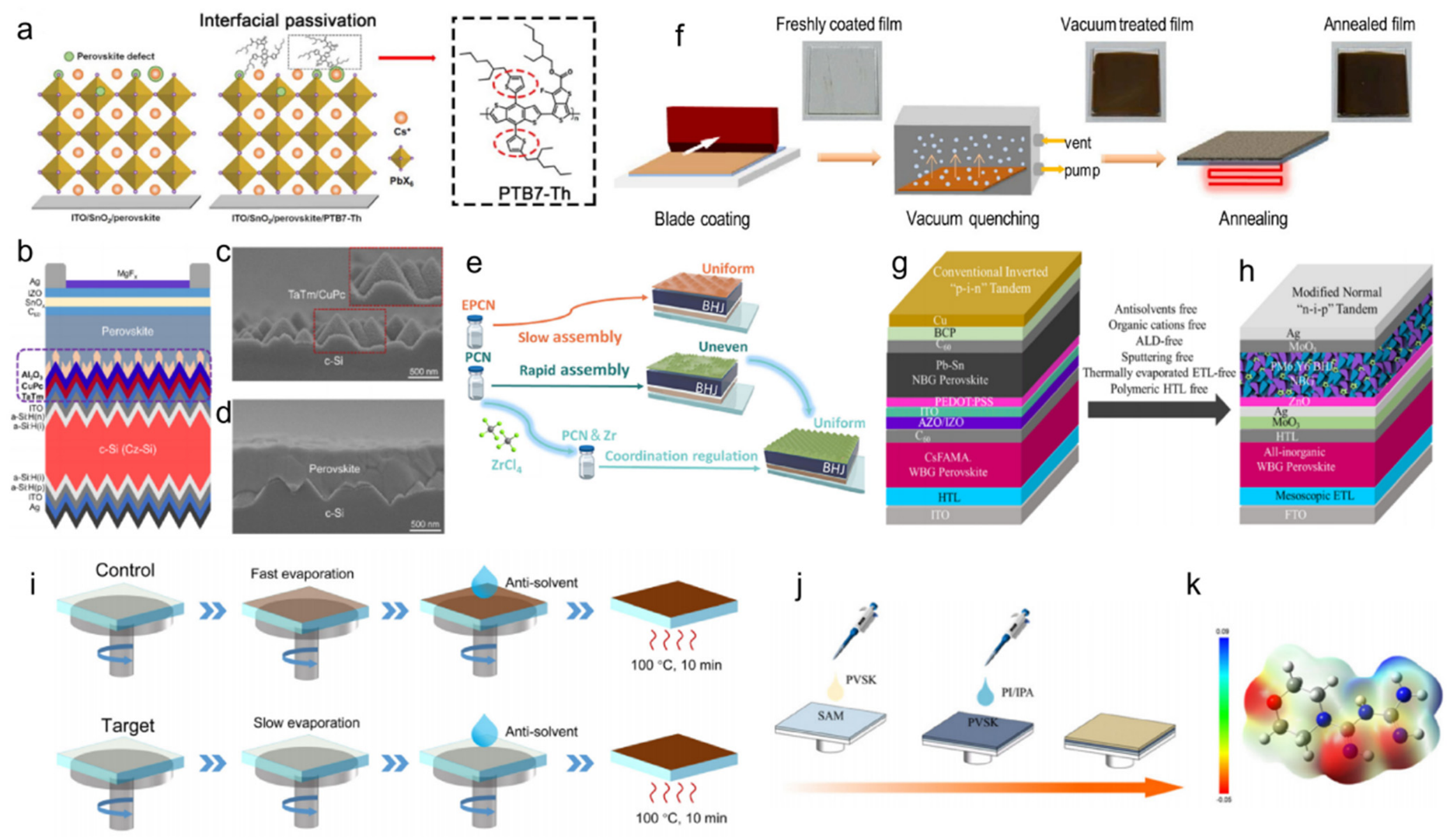
3.4.2. Interface Regulation
Interfacial engineering plays an equally vital role in determining the performance of perovskite/organic TSCs by minimizing non-radiative recombination, optimizing energy-level alignment, and facilitating efficient charge extraction across heterojunctions. An optoelectronic model combining Monte Carlo simulations with sensitivity analysis was developed to investigate two-terminal perovskite/organic TSCs, identifying key performance parameters and recombination losses. By optimizing the perovskite hole mobility and layer thicknesses, interfacial recombination was effectively reduced, yielding a device efficiency of 23.6% and outlining a pathway toward 28% efficiency [183]. High-color-fidelity semi-transparent perovskite/organic TSCs were developed by using a systematic selection method, in which the visible EQE fluctuation factor was employed to select CsPbI2Br as the front sub-cell and the NIR absorption selection factor was used to evaluate PTB7-Th:IEICO-4F as the rear sub-cell. Notably, the sulfur atoms in PTB7-Th bonded with Pb2+ to passivate halogen vacancies in CsPbI2Br (Figure 13a), effectively reducing interfacial recombination and aiding charge extraction, ultimately delivering a PCE of 24.3% with enhanced color fidelity [180].
Moving toward more sophisticated interfacial modulation strategies, a multilayer HTL structure composed of TaTm/CuPc/Al2O3 was developed for PSCs and textured perovskite/silicon tandem cells. In this architecture, CuPc ensured conformal coating and improved wetting, TaTm enhanced electron blocking, and the ultrathin Al2O3 layer effectively suppressed non-radiative recombination while reducing surface recombination without compromising carrier extraction (Figure 13b–d). This synergistic interfacial engineering approach enabled a p-i-n PSC to achieve a PCE of 24.5% with an impressive FF [181]. Most recently, plant Photosystem I (PSI) was integrated with C60 fullerene into a perovskite/organic TSC to address weak red-light absorption. PSI enhanced photon harvesting in the red spectral region, while C60 improved charge extraction and reduced non-radiative recombination losses, yielding a tandem PCE of 20.24% [184]. Concurrently, two pyrazine-based molecules, EPCN and PCN, were designed, and the assembly of PCN was regulated via a metal coordination strategy. Coordination of PCN with zirconium enhanced charge transport and light scattering in the organic sub-cell, while PCN also effectively passivated perovskite defects and modulated the Fermi level at the interface (Figure 13e). This multifunctional interfacial layer enabled a four-terminal perovskite/organic TSC to achieve a PCE of 25.43%, representing one of the highest efficiencies reported in this category [182].
In other words, the progression of interfacial engineering strategies in perovskite/organic TSCs reflects a clear evolution from empirical optimization toward rational design, encompassing optoelectronic modeling, defect passivation, multilayer charge-transport architectures, and even bio-inspired integration, all of which contribute to pushing device efficiencies beyond 25% while simultaneously addressing stability and functional requirements such as color fidelity. Thin buffer layers prevent solvent erosion of organic films, while conjugated SAMs optimize energy alignment without sacrificing near-infrared transmission.
3.4.3. Transport-Layer Strategies
Transport-layer engineering plays a critical role in perovskite/organic TSCs by regulating interfacial energetics, suppressing parasitic absorption, facilitating carrier recombination, and enabling efficient current matching between sub-cells. Early efforts focused primarily on transparent conductive electrodes and RL design. Hydrogenated indium oxide (IO:H) electrodes were introduced via magnetron sputtering in four-terminal perovskite/CIS TSCs, where H+ passivates oxygen vacancies to reduce carrier scattering, and O2 suppresses metallic indium formation to enhance transparency (Figure 13a). The resulting IO:H films exhibit reduced near-infrared parasitic absorption compared with IZO, enabling improved current matching and a PCE of 24.6% [185]. Subsequently, polyTPD was utilized as the hole-transport material in the interconnection layer of monolithic perovskite/organic TSCs. Its low optical absorption, appropriate hole mobility, and quasi-Ohmic contact reduce interfacial barriers, suppress hole accumulation (Figure 13b,c), and minimize voltage loss, leading to a PCE of 21.1% in CsPbI2Br/PM6:Y6-BO devices [186].
Building on RL optimization, a metal-free interconnection layer was constructed by combining ALD-grown SnO2 with diluted PEDOT:PSS, which avoids metal-induced parasitic absorption, ensures Ohmic contact, and allows the perovskite layer to filter ultraviolet light, achieving a tandem efficiency of 17.6% [187]. In parallel, from the perspective of HTL design, the dopant-free polymer PTQ10 was introduced as an HTL with interconnection functionality in CsPbI2Br-based devices. Its deep HOMO improves energy-level alignment, while S, N, and F atoms passivate surface defects and maintain efficient carrier transport (Figure 13d), thereby reducing voltage loss and improving current matching [188]. Further molecular engineering employed D-π-A polymers (PE51–PE53) as HTLs, where the longer side chains in PE53 promote face-on packing, enhance hole mobility (Figure 13e), and suppress recombination, enabling a tandem PCE of 23.07% [189].
With increasing emphasis on synergistic electrical and optical regulation, both transport layers and active layer morphology were optimized in inorganic perovskite/organic TSCs. Cl@MZO was employed as the ETL to improve energy-level alignment and reduce defect density, while the PM6:BTP-eC9 ratio (1:1.8) was tuned to enhance absorption and balance current between sub-cells, resulting in a PCE of 24.07% [190]. More recently, transport-layer design has evolved toward integrated optical–electrical modulation. Evaporated MoOx was replaced with solution-processed PEDOT:F in the interconnection layer, where its low surface energy controls Au diffusion to form smaller and more uniform nanoparticles (Figure 13f), shifting plasmonic absorption away from the near-infrared region and reducing optical loss while maintaining efficient recombination, achieving a PCE of 25.34% [191].
Molecular-level interfacial engineering has further improved transport properties. A volatile additive (TCB) strategy was developed to regulate SAM-based HTLs (Figure 13h), where noncovalent interactions induce ordered face-on stacking after additive evaporation, enhancing hole mobility, reducing interfacial recombination, and optimizing surface energy for improved upper-layer crystallinity and phase separation, leading to a tandem efficiency of 26.09% [192]. Meanwhile, PEDOT:PSS-based interconnection layers were optimized via 2PACz modification to tune surface coverage, which enhances charge extraction, balances recombination within the ICL (Figure 13g), and reduces parasitic absorption, resulting in a PCE of 25.26% with improved device stability [193]. These advances highlight the importance of simultaneously optimizing interfacial energetics and optical properties within transport and RLs.
Overall, transport-layer strategies in perovskite/organic TSCs have evolved from initial electrode and RL optimization toward molecular-level interfacial engineering and optical–electrical synergistic regulation, enabling efficient carrier transport, reduced energy loss, and tandem efficiencies exceeding 25%. Table 11 summarizes of device performance parameters of typical perovskite/organic TSCs. Dopant-free polymer transport materials match low-temperature organic processing best. Inorganic oxide layers improve mobility but introduce thermal-incompatibility issues. Perovskite/organic TSCs are limited by organic thermal instability, so low-temperature crystallization and mild interface treatment are the only viable high-performance strategies.
Table 11.
Summary of device performance parameters of typical perovskite/organic TSCs.
Figure 13.
(a) Scheme of the 4-T perovskite/CIS TSCs. Reprint with permission [185]. Copyright 2020, American Chemical Society. (b) Device structure, cross-sectional scanning electron microscopy image. (c) Hole-transport materials: polyTPD, PBDB-T-Si, and D18. Reprint with permission [186]. Copyright 2021, American Chemical Society. (d) Device structure of CsPbI2Br PSCs and molecule structures of PTQ10 and P3HT. Reprint with permission [188]. Copyright 2022, Elsevier. (e) Device structure of TSCs and the molecule structure of D18 and Y6. Reprint with permission [189]. Copyright 2022, Elsevier. (f) Schematic illustration of possible mechanism. Reprint with permission [191]. Copyright 2025, Springer Nature. (g) Schematic illustration of the coverage state and in situ washing of 2PACz. Reprint with permission [193]. Copyright 2021, American Chemical Society. (h) Schematic plot showing that a more ordered stacking with a face-on feature formed after TCB treatment. Reprint with permission [192]. Copyright 2025, Royal Society of Chemistry.
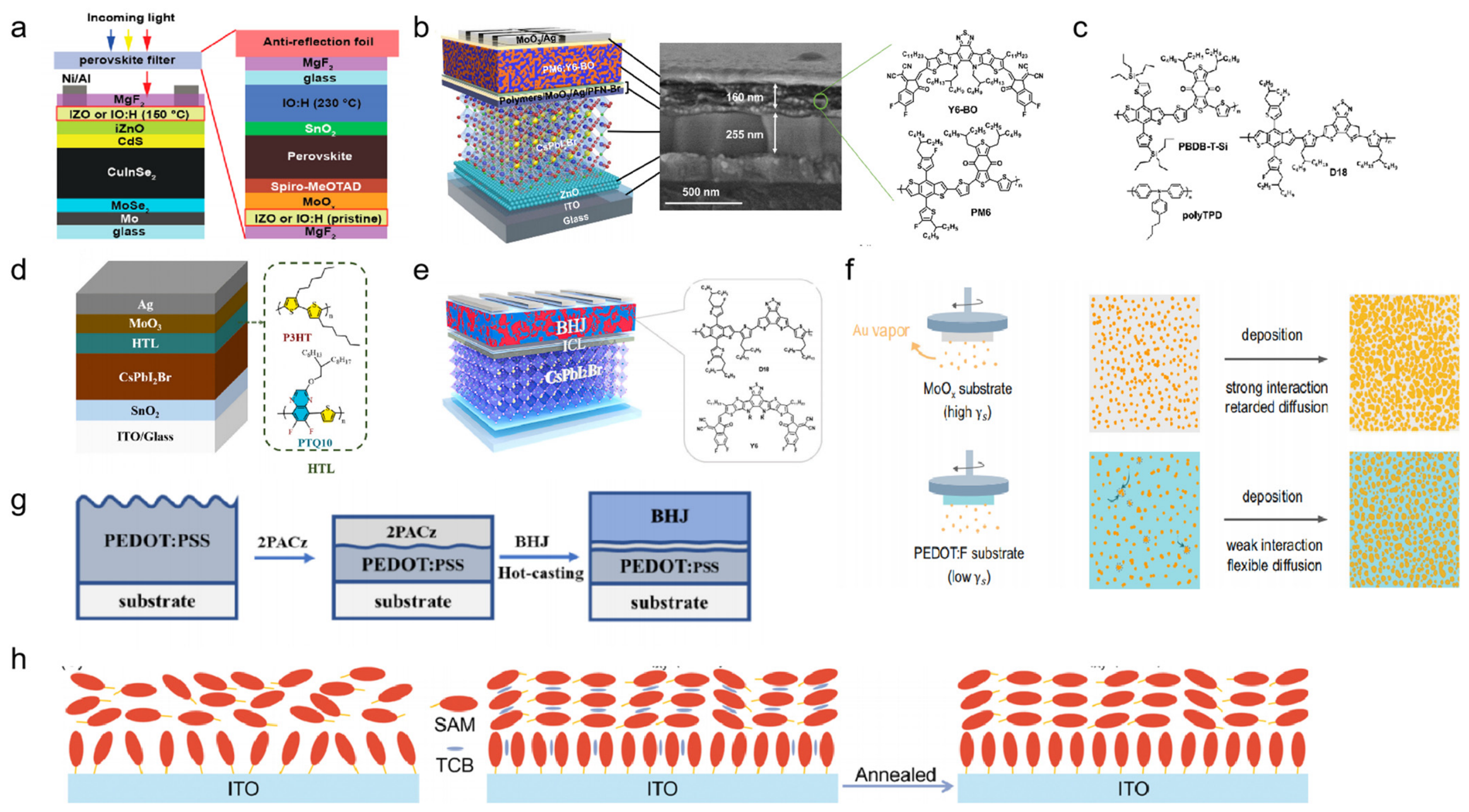
4. Challenges, Opportunities, and Future Perspectives of Perovskite TSCs
4.1. Core Challenges
Material-related challenges: Despite significant progress in perovskite TSCs, several material-related challenges persist. A primary concern is the instability of perovskite materials, which can cause device performance to degrade over time. Perovskites are inherently sensitive to humidity, temperature, and light exposure. Therefore, developing stable compositions and robust device architectures is essential for commercialization. Another challenge is the toxicity of certain constituents, most notably lead (Pb). As a toxic heavy metal, lead raises environmental and health concerns. To address this, substantial efforts have been directed toward lead-free perovskites based on tin (Sn), bismuth (Bi), or antimony (Sb). However, the performance of these lead-free alternatives still lags behind that of their lead-based counterparts. For example, recent reviews have noted that, while tin-based perovskites offer favorable bandgaps, their efficiency remains limited by large Voc and FF losses [194], and further research is needed to improve their optoelectronic properties and stability. Scalability of perovskite synthesis represents an additional hurdle. Current laboratory-scale methods, such as solution processing and vapor deposition, are not readily transferable to high-volume production. The development of scalable, cost-effective routes to high-quality perovskite materials is therefore critical for commercial viability.
Intrinsic fundamental limitations of four tandem architectures: From the perspective of intrinsic structural and material limitations, the four mainstream perovskite tandem architectures each face distinct fundamental bottlenecks. Perovskite/silicon TSCs are constrained by bandgap mismatch (~1.6–1.7 eV vs. 1.12 eV of Si) causing current mismatch, and textured Si substrates inevitably induce uneven film growth and sputtering damage. All-perovskite TSCs suffer from light-induced halide segregation in WBG perovskites and rapid Sn2+ oxidation in NBG Pb-Sn perovskites, while the ~0.5 eV bandgap offset limits theoretical efficiency. Perovskite/CIGS devices are hindered by lattice mismatch and dense interfacial traps, with the narrow CIGS bandgap (~1.0 eV) forcing a current–voltage trade-off. Perovskite/organic TSCs are fundamentally limited by weak NIR absorption, low carrier mobility of organic layers, and thermal incompatibility between solution-processed perovskites and vacuum-deposited organic films. These architecture-specific constraints cannot be completely resolved by conventional passivation or compositional tuning, and remain the root obstacles to further efficiency breakthroughs. Beyond these inherent limitations, additional material-, fabrication-, and cost-related challenges persist.
Device fabrication and integration challenges: Fabricating and integrating perovskite TSCs also presents considerable difficulties. One major challenge is the development of efficient, stable RLs to connect the two sub-cells. The inter-sub-cell interface can introduce significant recombination losses, diminishing tandem efficiency. As highlighted by Li et al. in their review of perovskite/silicon TSCs, charge-transport inefficiencies in interconnecting layers remain a key obstacle to optimal device performance [195]. High-quality RLs with low resistance and excellent charge-transfer properties are therefore essential. Another fabrication challenge is controlling the thickness and uniformity of the perovskite and charge-transport layers. Device performance is highly sensitive to these parameters, and even small variations can cause substantial degradation. Achieving precise thickness and uniformity over large areas is especially demanding for mass production. Advanced deposition techniques such as atomic layer deposition and slot-die coating show promise, but further optimization is required to ensure consistent performance across large-area devices [196]. Module-level integration introduces further complexity. Connecting multiple cells in series or parallel can generate additional losses from interconnections, edge effects, and non-uniformity. Reliable and efficient module designs and fabrication processes are therefore needed to translate the high efficiencies of small-area tandem cells into practical large-scale devices.
Cost and commercialization barriers: Although perovskite TSCs offer impressive efficiency potential, their commercialization faces several cost-related barriers. Materials, fabrication, and module integration must be cost-competitive with established photovoltaic technologies such as silicon. While perovskite materials themselves can be low-cost and solution-processable, the need for high-purity materials, precise fabrication, and robust encapsulation to ensure long-term stability may increase overall costs. The absence of standardized, low-cost manufacturing protocols for large-area tandem devices remains a major obstacle [197]. Additionally, the relatively high cost of certain charge-transport materials (e.g., spiro-OMeTAD) and transparent electrodes (e.g., ITO) further hinders cost reduction [198,199]. Addressing these barriers requires not only material substitution but also process simplification and yield improvement.
Cross-system stability comparison of four tandem structures: The four perovskite tandem architectures exhibit obvious differences in long-term operational stability under unified ISOS standard test conditions. Perovskite/silicon TSCs possess the best overall stability. Silicon substrates have stable chemical properties and low ion-migration risks. After triple-halide passivation and interface optimization, encapsulated devices can retain over 80% initial efficiency after 1000 h damp heat aging. Perovskite/CIGS TSCs rank second. Flexible PI substrates introduce interfacial stress, accelerating ion diffusion, so unencapsulated devices degrade rapidly under high humidity. All-perovskite TSCs face the worst stability bottlenecks. WBG layers suffer light-induced halide segregation, while NBG Sn-Pb perovskites are prone to oxidation, leading to obvious efficiency decay within hundreds of hours without full inert encapsulation. Perovskite/organic TSCs are limited by organic-layer thermal phase separation. High temperature and continuous illumination cause irreversible absorption loss of organic sub-cells, restricting long-term output stability. In addition, for any single tandem system, composite modification combining component regulation and interface passivation always achieves far better stability improvement than adopting only one single optimization strategy. Different tandem architectures show completely different responses to identical modification strategies, determined by substrate thermal stability, lattice matching, and processing-temperature windows.
4.2. Future Perspectives
Material development: Future advances in perovskite TSCs will depend heavily on the development of new materials. A key focus area is lead-free perovskites with high efficiency and stability. Although progress has been made, their performance still trails that of lead-based systems. For instance, Li et al. recently observed that tin-based perovskites continue to suffer from poor crystallization quality, high defect densities, and severe non-radiative recombination at buried interfaces [200]. Further fundamental understanding and strategies to enhance carrier mobility and reduce defect densities are needed. Another direction is the exploration of perovskite compositions with tunable bandgaps beyond the current range, enabling more flexible tandem architectures and better current matching with diverse bottom-cell materials. The development of new charge-transport materials with high conductivity, transparency, and stability is equally important for minimizing losses in tandem devices [201].
Device engineering: Advances in device engineering will also play a vital role. Novel architectures, such as multi-junction TSCs with three or more sub-cells, could further boost efficiency by capturing a broader portion of the solar spectrum. Realizing this potential, however, demands precise bandgap control and efficient charge transfer between sub-cells. Interface optimization is another critical area. Improving interfacial quality can reduce recombination losses and enhance charge transport. Techniques such as surface passivation and interface engineering with SAMs are promising for addressing these issues [202].
Scale-up and manufacturing: To realize the commercial promise of TSCs, substantial progress in scale-up and manufacturing is necessary. High-throughput, low-cost large-area fabrication techniques must be developed. Roll-to-roll processing, widely used in flexible electronics, is a promising route for large-scale manufacturing, but challenges related to uniformity and reproducibility must be overcome. Reliable encapsulation techniques for large-area modules are equally critical for long-term stability. Encapsulation materials and processes must be cost-effective, compatible with high-volume production, and capable of providing effective protection against environmental degradation.
Integration and commercialization pathways: Integrating perovskite TSCs with other technologies will open new application opportunities. For example, combining tandem cells with energy storage systems could enable self-sustaining energy solutions, while integration with smart-grid technologies can facilitate more efficient solar energy management and distribution. Building-integrated photovoltaics (BIPV) represents another impactful area. The flexibility, light weight, and potential semi-transparency of perovskite TSCs make them ideal for facades, windows, and rooftops, turning buildings into active energy generators. As noted by Tiwari in a review of self-powered IoT devices, emerging photovoltaics including silicon/perovskite tandem cells can offer superior solutions for applications requiring energy autonomy and sustainable operation [203]. Beyond BIPV, portable electronics, drones, and space technologies constitute attractive niches where the high specific power of perovskite TSCs could be particularly advantageous. Although current manufacturing costs remain relatively high, continued progress in scalable fabrication and encapsulation may eventually enable cost-competitive utility-scale deployment. Furthermore, integrating perovskite top cells into existing silicon bottom-cell production lines offers a promising pathway toward commercial entry.
4.3. Standardization of Photovoltaic Stability Characterization Protocols
The current literature adopts diverse stability test conditions (MPP tracking, damp-heat aging, light soaking, and thermal cycling), leading to inconsistent T80/T90 lifetime metrics that hinder cross-study quantitative comparison. The International Stability Testing Operating Standards (ISOS) series provides unified standardized testing frameworks for perovskite photovoltaic devices, which should be uniformly followed in future experimental reports.
Key recommended reporting specifications are summarized as follows: Mandatory full environmental parameters: Test temperature, relative humidity (RH), illumination intensity (1 sun/AM1.5G), inert/air atmosphere, and encapsulation architecture (glass–glass, foil encapsulation, and unencapsulated) must be explicitly listed alongside PCE retention data (T80/T90, MPP retention hours).
For unified stability evaluation, ISOS tests are classified into three standard categories. ISOS-L is a continuous light soaking test conducted under operational MPP tracking, which is the test protocol most representative of real-world working conditions. ISOS-D refers to the dark damp-heat aging test performed at 85 °C and 85% relative humidity, serving as an accelerated test to characterize humidity-induced degradation. ISOS-T is the thermal cycling test, designed to simulate day-night temperature fluctuations that devices would experience in practical operation.
5. Conclusions
Perovskite TSCs offer a compelling pathway to surpass the Shockley–Queisser limit of single-junction photovoltaics. This review has systematically surveyed recent progress across four major configurations, namely perovskite/silicon, perovskite/CIGS, all-perovskite, and perovskite/organic TSCs, covering their working principles, optimization strategies, and remaining challenges.
Perovskite/silicon TSCs have achieved certified efficiencies beyond 34%, driven by compositional engineering, multifunctional defect passivation, crystallization control on textured substrates, and interface engineering with SAMs. These approaches have also improved device stability. Perovskite/CIGS TSCs have approached 30% efficiency through bandgap matching and interfacial modification, with promising results on flexible substrates. All-perovskite TSCs have surpassed 28% by effectively suppressing halide segregation in WBG cells and mitigating Sn-Pb oxidation in NBG cells. Perovskite/organic TSCs, though less mature, have rapidly advanced beyond 25% efficiency, benefiting from innovative interconnection layers, quasi-2D/3D heterojunctions, and molecular additives that stabilize mixed-halide perovskites.
Nevertheless, critical challenges persist. The inherent instability of perovskite materials under moisture, oxygen, thermal stress, and prolonged illumination demands robust encapsulation and intrinsically stable compositions. Halide phase segregation continues to impair the performance and lifetime of WBG perovskites. Lead toxicity necessitates the exploration of tin-based and other alternative materials, although their efficiencies and stabilities currently lag behind. Moreover, scaling up from laboratory cells to large-area modules, developing efficient and transparent RLs, and achieving cost competitiveness with established silicon technology remain essential for commercialization.
Future research should prioritize lead-free perovskites with improved optoelectronic properties, advanced encapsulation techniques such as atomic layer deposition, and novel charge-transport materials that minimize energy losses. Scalable manufacturing methods, including blade coating, slot-die coating, and roll-to-roll processing, must be refined for high-throughput production. Integrating tandem cells with energy storage systems, building-integrated photovoltaics, and portable electronics could further broaden their application scope.
In summary, perovskite TSCs represent one of the most promising routes to next-generation high-efficiency photovoltaics. Sustained interdisciplinary efforts in materials science, device engineering, and manufacturing will be key to overcoming existing barriers and accelerating the global transition to sustainable energy. The ultimate commercial success will depend on the synergistic advancement of efficiency, stability, and scalability.
Author Contributions
The initial manuscript was prepared by T.H., K.X. and X.W.; X.L. and D.Y. conceived the research concept, critically reviewed and edited the manuscript, and contributed to the acquisition of funding. All authors have read and agreed to the published version of the manuscript.
Funding
This research was funded by [National Natural Science Foundation of China] grant number [62541403].
Data Availability Statement
No new data were created or analyzed in this study. Data sharing is not applicable to this article.
Acknowledgments
The authors gratefully acknowledge financial support from the National Natural Science Foundation of China (62541403).
Conflicts of Interest
The authors declare no conflicts of interest.
References
- Yoshikawa, K.; Kawasaki, H.; Yoshida, W.; Irie, T.; Konishi, K.; Nakano, K.; Uto, T.; Adachi, D.; Kanematsu, M.; Uzu, H.; et al. Silicon Heterojunction Solar Cell with Interdigitated Back Contacts for a Photoconversion Efficiency over 26%. Nat. Energy 2017, 2, 17032. [Google Scholar] [CrossRef] [Scilit]
- Wang, R.; Han, M.; Wang, Y.; Zhao, J.; Zhang, J.; Ding, Y.; Zhao, Y.; Zhang, X.; Hou, G. Recent Progress on Efficient Perovskite/Organic Tandem Solar Cells. J. Energy Chem. 2023, 83, 158–172. [Google Scholar] [CrossRef] [Scilit]
- Cheng, Z.; Zhang, M.; Zhang, Y.; Qi, W.; Wang, Z.; Liu, B.; Di, D. Stable Wide-Bandgap Perovskite Solar Cells for Tandem Applications. Nano Energy 2024, 127, 109708. [Google Scholar] [CrossRef] [Scilit]
- Parida, B.; Baloch, A.A.B.; Albadwawi, O.; Adothu, B.; Aly, S.P.; Alberts, V.; Sundaray, M. Solution and Vacuum-Based Scalable Deposition Methods for Perovskite/Si Tandem Solar Cells. Adv. Opt. Mater. 2026, 14, e03341. [Google Scholar] [CrossRef] [Scilit]
- De Bastiani, M.; Subbiah, A.S.; Babics, M.; Ugur, E.; Xu, L.; Liu, J.; Allen, T.G.; Aydin, E.; De Wolf, S. Bifacial Perovskite/Silicon Tandem Solar Cells. Joule 2022, 6, 1431–1445. [Google Scholar] [CrossRef] [Scilit]
- Liu, W.; Duan, Y.; Zhang, Z.; Gao, J.; Li, S.; Fink, Z.; Wu, X.; Ma, Z.; Saeki, A.; Russell, T.P.; et al. Rational Organic Subcell Engineering Enables Efficient Organic-Perovskite Tandem Solar Cells. ACS Energy Lett. 2023, 8, 4514–4523. [Google Scholar] [CrossRef] [Scilit]
- Ašmontas, S.; Mujahid, M. Recent Progress in Perovskite Tandem Solar Cells. Nanomaterials 2023, 13, 1886. [Google Scholar] [CrossRef] [Scilit] [PubMed]
- Bailie, C.D.; McGehee, M.D. High-Efficiency Tandem Perovskite Solar Cells. MRS Bull. 2015, 40, 681–685. [Google Scholar] [CrossRef] [Scilit]
- Wali, Q.; Elumalai, N.K.; Iqbal, Y.; Uddin, A.; Jose, R. Tandem Perovskite Solar Cells. Renew. Sustain. Energy Rev. 2018, 84, 89–110. [Google Scholar] [CrossRef] [Scilit]
- Green, M.A. Third Generation Photovoltaics: Ultra-High Conversion Efficiency at Low Cost. Prog. Photovolt. Res. Appl. 2001, 9, 123–135. [Google Scholar] [CrossRef] [Scilit]
- Bonnet-Eymard, M.; Boccard, M.; Bugnon, G.; Meillaud, F.; Despeisse, M.; Haug, F.-J.; Ballif, C. Current Matching Optimization in High-Efficiency Thin-Film Silicon Tandem Solar Cells. In Conference Record of the IEEE Photovoltaic Specialists Conference; IEEE: Piscataway, NJ, USA, 2013; pp. 0184–0187. [Google Scholar] [CrossRef] [Scilit]
- Pan, H.; Shao, H.; Zhang, X.L.; Shen, Y.; Wang, M. Interface Engineering for High-Efficiency Perovskite Solar Cells. J. Appl. Phys. 2021, 129, 130904. [Google Scholar] [CrossRef] [Scilit]
- Sato, Y.; Matsui, T.; Ikeda, T.; Wada, H.; Sai, H. Size-Dependent Mechanical Strength of Pyramidal-Textured Si Wafers from Nanoscale to Microscale and Its Implications for Si Heterojunction and Perovskite/Si Tandem Solar Cells. Sol. Energy Mater. Sol. Cells 2026, 301, 114307. [Google Scholar] [CrossRef] [Scilit]
- Li, Y.; Hu, H.; Chen, B.; Salim, T.; Zhang, J.; Ding, J.; Yuan, N.; Lam, Y.M. Reflective Perovskite Solar Cells for Efficient Tandem Applications. J. Mater. Chem. C 2017, 5, 134–139. [Google Scholar] [CrossRef] [Scilit]
- Cherif, F.E.; Sammouda, H. Optoelectronic Simulation and Optimization of Tandem and Multi-Junction Perovskite Solar Cells Using Concentrating Photovoltaic Systems. Energy Rep. 2021, 7, 5895–5908. [Google Scholar] [CrossRef] [Scilit]
- Chantana, J.; Takeguchi, K.; Kawano, Y.; Minemoto, T. Estimation of Annual Energy Generation of Perovskite/Crystalline Si Tandem Solar Cells with Different Configurations in Central Part of Japan. Renew. Energy 2022, 195, 896–905. [Google Scholar] [CrossRef] [Scilit]
- Wu, Y.; Yan, D.; Peng, J.; Duong, T.; Wan, Y.; Phang, S.P.; Shen, H.; Wu, N.; Barugkin, C.; Fu, X.; et al. Monolithic Perovskite/Silicon-Homojunction Tandem Solar Cell with over 22% Efficiency. Energy Environ. Sci. 2017, 10, 2472–2479. [Google Scholar] [CrossRef] [Scilit]
- Gupta, R.K.; Kumar, D.K.; Sudhakar, V.; Beckedahl, J.M.; Abate, A.; Katz, E.A.; Visoly-Fisher, I. Seasonal Effects on Outdoor Stability of Perovskite Solar Cells. Adv. Energy Mater. 2025, 15, 2403844. [Google Scholar] [CrossRef] [Scilit]
- De Bastiani, M.; Mirabelli, A.J.; Hou, Y.; Gota, F.; Aydin, E.; Allen, T.G.; Troughton, J.; Subbiah, A.S.; Isikgor, F.H.; Liu, J.; et al. Efficient Bifacial Monolithic Perovskite/Silicon Tandem Solar Cells via Bandgap Engineering. Nat. Energy 2021, 6, 167–175. [Google Scholar] [CrossRef] [Scilit]
- Xu, J.; Boyd, C.C.; Yu, Z.J.; Palmstrom, A.F.; Witter, D.J.; Larson, B.W.; France, R.M.; Werner, J.; Harvey, S.P.; Wolf, E.J.; et al. Triple-Halide Wide-Band Gap Perovskites with Suppressed Phase Segregation for Efficient Tandems. Science 2020, 367, 1097–1104. [Google Scholar] [CrossRef] [Scilit] [PubMed]
- Huang, Y.C.; Huang, S.W.; Li, C.F.; Huang, S.H.; Tsai, F.Y.; Su, W.F. A Comprehensive Optimization of Highly Efficient MA-Free Wide-Bandgap Perovskites for 4-T Perovskite/Silicon Tandem Solar Cells. Chem. Eng. J. 2025, 503, 158272. [Google Scholar] [CrossRef] [Scilit]
- Gao, C.; Zhang, H.; Ma, S.; Su, H.; Huang, H.; He, L.; Zhang, D.; Du, D.; Liu, H.; Shen, W. Quasi-Conformal Monolithic n-i-p Perovskite/c-Si Tandem Solar Cells with Light Management Strategies Exceed 28% Efficiency. Nano Energy 2024, 129, 110066. [Google Scholar] [CrossRef] [Scilit]
- Pan, H.; Zhou, Y.; Fu, M.; Yin, J.; Chen, Z.; Zhang, L.; Wei, Y.; Tian, J. Investigation of Bandgaps and Thicknesses of Sub-Cells on the Performance of Lead-Free CsSnX3/Si Tandem Solar Cells via SCAPS-1D. Mater. Sci. Eng. B 2025, 321, 118479. [Google Scholar] [CrossRef] [Scilit]
- Shi, B.; Liu, P.; Sunli, Z.; Han, W.; Sun, C.; Liu, Y.; Luo, Y.; Si, J.; Du, P.; Zhang, F.; et al. Halogen Anion Pre-Homogenization of Sequentially Deposited Wide Bandgap Perovskites for Commercial Textured Perovskite/Silicon Tandem Solar Cells. Energy Environ. Sci. 2025, 18, 6297–6306. [Google Scholar] [CrossRef] [Scilit]
- Ugur, E.; Said, A.A.; Dally, P.; Zhang, S.; Petoukhoff, C.E.; Rosas-Villalva, D.; Zhumagali, S.; Yildirim, B.K.; Razzaq, A.; Sarwade, S.; et al. Enhanced Cation Interaction in Perovskites for Efficient Tandem Solar Cells with Silicon. Science 2024, 385, 533–538. [Google Scholar] [CrossRef] [Scilit] [PubMed]
- Liu, J.; Aydin, E.; Yin, J.; De Bastiani, M.; Isikgor, F.H.; Rehman, A.U.; Yengel, E.; Ugur, E.; Harrison, G.T.; Wang, M.; et al. 28.2%-Efficient, Outdoor-Stable Perovskite/Silicon Tandem Solar Cell. Joule 2021, 5, 3169–3186. [Google Scholar] [CrossRef] [Scilit]
- Yao, Y.; Hang, P.; Li, B.; Hu, Z.; Kan, C.; Xie, J.; Wang, Y.; Zhang, Y.; Yang, D.; Yu, X. Phase-Stable Wide-Bandgap Perovskites for Four-Terminal Perovskite/Silicon Tandem Solar Cells with Over 30% Efficiency. Small 2022, 18, 2203319. [Google Scholar] [CrossRef] [Scilit] [PubMed]
- Tong, J.; Song, Z.; Kim, D.H.; Chen, X.; Chen, C.; Palmstrom, A.F.; Ndione, P.F.; Reese, M.O.; Dunfield, S.P.; Reid, O.G.; et al. Carrier lifetimes of >1 μs in Sn-Pb perovskites enable efficient all-perovskite tandem solar cells. Science 2019, 364, 475–479. [Google Scholar] [CrossRef] [Scilit] [PubMed]
- Wang, S.; Shao, Y.; Dai, W.; Wang, K.; Dong, X.; Luo, T.; He, Y.; Liu, S.; Wan, L.; Li, D.; et al. Sweet Zwitterionic Aspartame for High-Performance Wide-Bandgap Perovskite Solar Cells and Tandem Devices. Adv. Funct. Mater. 2025, 35, 2503592. [Google Scholar] [CrossRef] [Scilit]
- Yang, X.; Song, Q.; Liu, Y.; Yang, L.; Yan, Y.; Huang, J.; Yang, L.; Zhu, X.; Zhao, Q.; Ji, X.; et al. A Multifunctional Additive for Enhancing the Performance of Single-Junction Perovskite and Perovskite/Silicon Tandem Solar Cells. J. Mater. Chem. C 2025, 13, 9285–9293. [Google Scholar] [CrossRef] [Scilit]
- Fang, Z.; Deng, B.; Jin, Y.; Yang, L.; Chen, L.; Zhong, Y.; Feng, H.; Yin, Y.; Liu, K.; Li, Y.; et al. Surface Reconstruction of Wide-Bandgap Perovskites Enables Efficient Perovskite/Silicon Tandem Solar Cells. Nat. Commun. 2024, 15, 10554. [Google Scholar] [CrossRef] [Scilit] [PubMed]
- Nonni, E.; Matteocci, F.; Serenelli, L.; Castriotta, L.A.; Barichello, J.; Magliano, E.; Di Girolamo, D.; Martini, L.; Menchini, F.; Izzi, M.; et al. A Holistic Approach for a Large Area (>1 cm2) Mechanically Stacked Two Terminal Tandem Perovskite/Silicon Heterojunction with Efficiencies above 30%. Sol. Energy Mater. Sol. Cells 2025, 292, 113740. [Google Scholar] [CrossRef] [Scilit]
- Duong, T.; Nguyen, T.; Huang, K.; Pham, H.; Adhikari, S.G.; Khan, M.R.; Duan, L.; Liang, W.; Fong, K.C.; Shen, H.; et al. Bulk Incorporation with 4-Methylphenethylammonium Chloride for Efficient and Stable Methylammonium-Free Perovskite and Perovskite-Silicon Tandem Solar Cells. Adv. Energy Mater. 2023, 13, 2203607. [Google Scholar] [CrossRef] [Scilit]
- Luo, H.; Han, X.; Yang, B.; Ou, W.; Suo, J.; Sun, H.; Zheng, X.; Hong, J.; Chu, Z.; Zhao, L.; et al. Damp-Stable Perovskite/Silicon Tandem Solar Cells with Internal Encapsulating Sulfonium-Based Molecules. ACS Energy Lett. 2025, 10, 3325–3334. [Google Scholar] [CrossRef] [Scilit]
- Xu, F.; Aydin, E.; Liu, J.; Ugur, E.; Harrison, G.T.; Xu, L.; Vishal, B.; Yildirim, B.K.; Wang, M.; Ali, R.; et al. Monolithic Perovskite/Perovskite/Silicon Triple-Junction Solar Cells with Cation Double Displacement Enabled 2.0 EV Perovskites. Joule 2024, 8, 224–240. [Google Scholar] [CrossRef] [Scilit]
- Pei, F.; Chen, Y.; Wang, Q.; Li, L.; Ma, Y.; Liu, H.; Duan, Y.; Song, T.; Xie, H.; Liu, G.; et al. A Binary 2D Perovskite Passivation for Efficient and Stable Perovskite/Silicon Tandem Solar Cells. Nat. Commun. 2024, 15, 7024. [Google Scholar] [CrossRef] [Scilit] [PubMed]
- Sun, C.; Jin, L.; Wang, X.; Shi, B.; Wang, P.; Ren, N.; Han, X.; Sun, L.; Zhu, Z.; Huang, Q.; et al. Wide-Bandgap Perovskite and Perovskite/Silicon Tandem Solar Cells through Strong Hydrogen Bonding Interaction. ACS Energy Lett. 2025, 10, 2171–2179. [Google Scholar] [CrossRef] [Scilit]
- Xia, R.; Xu, Y.; Chen, B.; Kanda, H.; Franckevičius, M.; Gegevičius, R.; Wang, S.; Chen, Y.; Chen, D.; Ding, J.; et al. Interfacial Passivation of Wide-Bandgap Perovskite Solar Cells and Tandem Solar Cells. J. Mater. Chem. A 2021, 9, 21939–21947. [Google Scholar] [CrossRef] [Scilit]
- Zhu, W.; Yang, M.; Han, T.; Wang, Y.; Luo, X.; Chai, W.; Xi, H.; Zhou, L.; Chen, D.; Zhang, J.; et al. Homogeneous Crystallization of MA-Free, Wide-Bandgap Perovskite Films via Self-Assembled Monolayer Capping for Laminated Silicon/Perovskite Tandem Solar Cells. Chem. Eng. J. 2024, 500, 156798. [Google Scholar] [CrossRef] [Scilit]
- Qiang, Z.; Wu, Y.; Gao, X.; Gong, Y.; Liu, Y.; Zhao, X.; Tian, H.; Wang, W.; Wang, C.; Liu, W.; et al. A Scalable Method for Fabricating Monolithic Perovskite/Silicon Tandem Solar Cells Based on Low-Cost Industrial Silicon Bottom Cells. Chem. Eng. J. 2024, 495, 153422. [Google Scholar] [CrossRef] [Scilit]
- Kan, C.; Hang, P.; Wang, S.; Li, B.; Yu, X.; Yang, X.; Yao, Y.; Shi, W.; De Wolf, S.; Yin, J.; et al. Efficient and Stable Perovskite-Silicon Tandem Solar Cells with Copper Thiocyanate-Embedded Perovskite on Textured Silicon. Nat. Photonics 2025, 19, 63–70. [Google Scholar] [CrossRef] [Scilit]
- Chen, B.; Yu, Z.J.; Manzoor, S.; Wang, S.; Weigand, W.; Yu, Z.; Yang, G.; Ni, Z.; Dai, X.; Holman, Z.C.; et al. Blade-Coated Perovskites on Textured Silicon for 26%-Efficient Monolithic Perovskite/Silicon Tandem Solar Cells. Joule 2020, 4, 850–864. [Google Scholar] [CrossRef] [Scilit]
- Xu, K.; Al-Ashouri, A.; Peng, Z.W.; Köhnen, E.; Hempel, H.; Akhundova, F.; Marquez, J.A.; Tockhorn, P.; Shargaieva, O.; Ruske, F.; et al. Slot-Die Coated Triple-Halide Perovskites for Efficient and Scalable Perovskite/Silicon Tandem Solar Cells. ACS Energy Lett. 2022, 7, 3600–3611. [Google Scholar] [CrossRef] [Scilit] [PubMed]
- Das, A.; Rana, N.K.; Ravidas, B.K.; Ketaraju, S.; Komarala, V.K.; Samajdar, D.P.; Chander, N. Design and Investigation of Mixed-Halide Rb0.05Cs0.05MA0.15FA0.8Pb(I0.85Br0.15)3 on Crystalline Silicon Monolithic Tandem Solar Cell with Experimental Correlations of Sub Cells Utilizing SCAPS-1D Framework. J. Phys. Chem. Solids 2025, 200, 112541. [Google Scholar] [CrossRef] [Scilit]
- Zhang, Y.; Zhu, Y.; Sun, J.; Hu, M.; Chen, J.; Duan, B.; Hu, S.; Hou, P.; Tan, W.L.; Ku, Z.; et al. Low Pressure Chemical Vapor Deposited Perovskite Enables All Vacuum-Processed Monolithic Perovskite-Silicon Tandem Solar Cells. Adv. Energy Mater. 2025, 15, 2405377. [Google Scholar] [CrossRef] [Scilit]
- Chen, B.; Wang, P.; Li, R.; Ren, N.; Han, W.; Zhu, Z.; Wang, J.; Wang, S.; Shi, B.; Liu, J.; et al. A Two-Step Solution-Processed Wide-Bandgap Perovskite for Monolithic Silicon-Based Tandem Solar Cells with >27% Efficiency. ACS Energy Lett. 2022, 7, 2771–2780. [Google Scholar] [CrossRef] [Scilit]
- Golobostanfard, M.R.; Othman, M.; Turkay, D.; Artuk, K.; Chin, X.Y.; Mensi, M.D.; Jacobs, D.A.; Jeangros, Q.; Wolff, C.M.; Hessler-Wyser, A.; et al. Bifacial Perovskite/Silicon Heterojunction Tandem Solar Cells Based on FAPbI3-Based Perovskite via Hybrid Evaporation-Spin Coating. Nano Energy 2024, 131, 110269. [Google Scholar] [CrossRef] [Scilit]
- Li, Y.; Shi, B.; Xu, Q.; Yan, L.; Ren, N.; Li, Y.; Han, W.; Zhu, Z.; Zhang, Y.; Liu, J.; et al. CsCl Induced Efficient Fully-Textured Perovskite/Crystalline Silicon Tandem Solar Cell. Nano Energy 2024, 122, 109285. [Google Scholar] [CrossRef] [Scilit]
- Ma, S.; Zhu, W.; Han, T.; Zhang, C.; Gao, P.; Guo, Y.; Song, Z.; Ni, Y.; Qiao, D. Pure-Phase, Large-Grained Wide-Band-Gap Perovskite Films for High-Efficiency, Four-Terminal Perovskite/Silicon Tandem Solar Cells. ACS Appl. Mater. Interfaces 2023, 15, 40719–40726. [Google Scholar] [CrossRef] [Scilit] [PubMed]
- Lian, X.; Xu, Y.; Fu, W.; Meng, R.; Ma, Q.; Xu, C.; Luo, M.; Hu, Y.; Han, J.; Min, H.; et al. Homogenizing Morphology and Composition of Methylammonium-Free Wide-Bandgap Perovskite for Efficient and Stable Tandem Solar Cells. Adv. Funct. Mater. 2024, 34, 2402061. [Google Scholar] [CrossRef] [Scilit]
- Chen, Y.; Yang, N.; Zheng, G.; Pei, F.; Zhou, W.; Zhang, Y.; Li, L.; Huang, Z.; Liu, G.; Yin, R.; et al. Nuclei Engineering for Even Halide Distribution in Stable Perovskite/Silicon Tandem Solar Cells. Science 2024, 385, 554–560. [Google Scholar] [CrossRef] [Scilit] [PubMed]
- Er-raji, O.; Mahmoud, M.A.A.; Fischer, O.; Ramadan, A.J.; Bogachuk, D.; Reinholdt, A.; Schmitt, A.; Kore, B.P.; Gries, T.W.; Musiienko, A.; et al. Tailoring Perovskite Crystallization and Interfacial Passivation in Efficient, Fully Textured Perovskite Silicon Tandem Solar Cells. Joule 2024, 8, 2811–2833. [Google Scholar] [CrossRef] [Scilit]
- Fang, J.; Chen, W.; Yuan, S.; Yang, S.; Meng, H.; Mao, K.; Li, T.; Zhu, Z.; Feng, X.; Guo, H.; et al. Longitudinal Homogenized Intermediates Facilitate Air-Processed Hybrid Sequential Deposition of Perovskite/Silicon Tandem Solar Cells. ACS Mater. Lett. 2024, 6, 5066–5075. [Google Scholar] [CrossRef] [Scilit]
- Hossain, M.I.; Qarony, W.; Jovanov, V.; Tsang, Y.H.; Knipp, D. Nanophotonic Design of Perovskite/Silicon Tandem Solar Cells. J. Mater. Chem. A 2018, 6, 3625–3633. [Google Scholar] [CrossRef] [Scilit]
- Li, P.; Xiong, H.; Lin, L.; Jiang, L.; Kang, Z.; Yan, Q.; Lien, S.Y.; Chen, H.; Qiu, Y. Modeling and Simulation of Bifacial Perovskite/PERT-Silicon Tandem Solar Cells. Sol. Energy 2021, 227, 292–302. [Google Scholar] [CrossRef] [Scilit]
- Abbasiyan, A.; Noori, M.; Baghban, H. A Highly Efficient 4-Terminal Perovskite/Silicon Tandem Solar Cells Using QIBC and IBC Configurations in the Top and Bottom Cells, Respectively. Mater. Today Energy 2022, 28, 101055. [Google Scholar] [CrossRef] [Scilit]
- Du, D.; Gao, C.; Wang, H.; Shen, W. Photovoltaic Performance of Bifacial Perovskite/c-Si Tandem Solar Cells. J. Power Sources 2022, 540, 231622. [Google Scholar] [CrossRef] [Scilit]
- Ravidas, B.K.; Das, A.; Agnihotri, S.K.; Pandey, R.; Madan, J.; Hossain, M.K.; Roy, M.K.; Samajdar, D.P. Design Principles of Crystalline Silicon/CsGeI3 Perovskite Tandem Solar Cells Using a Combination of Density Functional Theory and SCAPS-1D Frameworks. Sol. Energy Mater. Sol. Cells 2024, 267, 112688. [Google Scholar] [CrossRef] [Scilit]
- Mondal, S.; Jain, A.; Maity, S. Exploring the Potential of Tin-Based Perovskite-Silicon Tandem Solar Cells through Numerical Analysis: A Pathway to Sustainable Energy Innovation. Sol. Energy Mater. Sol. Cells 2024, 271, 112869. [Google Scholar] [CrossRef] [Scilit]
- Yin, J.; Zhao, X.; Zhao, M.; Zhang, L.; Tian, J.; Wei, Y.; Ma, Z.; Zhou, Y. Effects of Subcell Bandgap Matching on the Performance of Perovskite/Cu(In,Ga)Se2 Tandem Solar Cells. Mater. Today Commun. 2024, 40, 109725. [Google Scholar] [CrossRef] [Scilit]
- Zhou, Y.P.; Chen, Y.; Li, J.Z.; Ran, C.X.; Wu, Z.B. Effects of Spatio-Temporal Variations of Solar Light on the Multiscale Optical and Electrical Characteristics of Ultrathin Tandem Solar Cells. Appl. Energy 2025, 377, 124526. [Google Scholar] [CrossRef] [Scilit]
- Sahli, F.; Werner, J.; Kamino, B.A.; Bräuninger, M.; Monnard, R.; Paviet-Salomon, B.; Barraud, L.; Ding, L.; Diaz Leon, J.J.; Sacchetto, D.; et al. Fully Textured Monolithic Perovskite/Silicon Tandem Solar Cells with 25.2% Power Conversion Efficiency. Nat. Mater. 2018, 17, 820–826. [Google Scholar] [CrossRef] [Scilit] [PubMed]
- Wang, S.; Wang, P.; Chen, B.; Li, R.; Ren, N.; Li, Y.; Shi, B.; Huang, Q.; Zhao, Y.; Grätzel, M.; et al. Suppressed Recombination for Monolithic Inorganic Perovskite/Silicon Tandem Solar Cells with an Approximate Efficiency of 23%. eScience 2022, 2, 339–346. [Google Scholar] [CrossRef] [Scilit]
- Zheng, J.; Duan, W.; Guo, Y.; Zhao, Z.C.; Yi, H.; Ma, F.J.; Granados Caro, L.; Yi, C.; Bing, J.; Tang, S.; et al. Efficient Monolithic Perovskite-Si Tandem Solar Cells Enabled by an Ultra-Thin Indium Tin Oxide Interlayer. Energy Environ. Sci. 2023, 16, 1223–1233. [Google Scholar] [CrossRef] [Scilit]
- Yang, G.; Yu, Z.J.; Wang, M.; Shi, Z.; Ni, Z.; Jiao, H.; Fei, C.; Wood, A.; Alasfour, A.; Chen, B.; et al. Shunt Mitigation toward Efficient Large-Area Perovskite-Silicon Tandem Solar Cells. Cell Rep. Phys. Sci. 2023, 4, 101628. [Google Scholar] [CrossRef] [Scilit]
- Li, J.; Farhadi, B.; Liu, S.; Liu, L.; Wang, H.; Du, M.; Yang, L.; Bao, S.; Zhang, S.T.; Li, D.; et al. Built-in Field Manipulation through a Perovskite Homojunction for Efficient Monolithic Perovskite/Silicon Tandem Solar Cells. Nano Energy 2024, 129, 109976. [Google Scholar] [CrossRef] [Scilit]
- Zheng, J.; Ning, D.; Li, Y.; Wang, Y.; Ma, Q.; Liu, L.; Yang, P.; He, W.; Yang, H.; Duan, W.; et al. Hybrid Interconnecting Layers Reduce Current Leakage Losses in Perovskite/Silicon Tandems with 81.8% Fill Factor. Cell Rep. Phys. Sci. 2024, 5, 102114. [Google Scholar] [CrossRef] [Scilit]
- Liu, J.; He, Y.; Ding, L.; Zhang, H.; Li, Q.; Jia, L.; Yu, J.; Lau, T.W.; Li, M.; Qin, Y.; et al. Perovskite/Silicon Tandem Solar Cells with Bilayer Interface Passivation. Nature 2024, 635, 596–603. [Google Scholar] [CrossRef] [Scilit] [PubMed]
- Guo, X.; Ying, Z.; Li, X.; Zhang, M.; Su, S.; Zheng, J.; Du, H.; Sun, Y.; Wu, J.; Liu, L.; et al. Oblique-Angle Damage-Free Evaporation of Silicon Oxide Electron-Selective Passivation Contacts for Efficient and Stable Perovskite and Perovskite/TOPCon Tandem Solar Cells. Adv. Energy Mater. 2025, 15, 2403021. [Google Scholar] [CrossRef] [Scilit]
- Magliano, E.; Di Giacomo, F.; Sathy, H.R.; Pourmotlagh, S.M.; Giliberti, G.; Becerril Rodriguez, D.; Ammirati, G.; Mariani, P.; Zarotti, F.; Matteocci, F.; et al. Solution-Processed Metal-Oxide Nanoparticles to Prevent The Sputtering Damage in Perovskite/Silicon Tandem Solar Cells. ACS Appl. Mater. Interfaces 2025, 17, 17599–17610. [Google Scholar] [CrossRef] [Scilit] [PubMed]
- Al-Ashouri, A.; Köhnen, E.; Li, B.; Magomedov, A.; Hempel, H.; Caprioglio, P.; Márquez, J.A.; Vilches, A.B.M.; Kasparavicius, E.; Smith, J.A.; et al. Monolithic Perovskite/Silicon Tandem Solar Cell with >29% Efficiency by Enhanced Hole Extraction. Science 2020, 370, 1300–1309. [Google Scholar] [CrossRef] [Scilit] [PubMed]
- Isikgor, F.H.; Furlan, F.; Liu, J.; Ugur, E.; Eswaran, M.K.; Subbiah, A.S.; Yengel, E.; De Bastiani, M.; Harrison, G.T.; Zhumagali, S.; et al. Concurrent Cationic and Anionic Perovskite Defect Passivation Enables 27.4% Perovskite/Silicon Tandems with Suppression of Halide Segregation. Joule 2021, 5, 1566–1586. [Google Scholar] [CrossRef] [Scilit]
- Aydin, E.; Liu, J.; Ugur, E.; Azmi, R.; Harrison, G.T.; Hou, Y.; Chen, B.; Zhumagali, S.; De Bastiani, M.; Wang, M.; et al. Ligand-Bridged Charge Extraction and Enhanced Quantum Efficiency Enable Efficient n-i-p Perovskite/Silicon Tandem Solar Cells. Energy Environ. Sci. 2021, 14, 4377–4390. [Google Scholar] [CrossRef] [Scilit]
- Xu, Q.; Shi, B.; Li, Y.; Yan, L.; Duan, W.; Li, Y.; Li, R.; Ren, N.; Han, W.; Liu, J.; et al. Conductive Passivator for Efficient Monolithic Perovskite/Silicon Tandem Solar Cell on Commercially Textured Silicon. Adv. Energy Mater. 2022, 12, 2202404. [Google Scholar] [CrossRef] [Scilit]
- Liu, Z.; Zhu, C.; Luo, H.; Kong, W.; Luo, X.; Wu, J.; Ding, C.; Chen, Y.; Wang, Y.; Wen, J.; et al. Grain Regrowth and Bifacial Passivation for High-Efficiency Wide-Bandgap Perovskite Solar Cells. Adv. Energy Mater. 2023, 13, 2203230. [Google Scholar] [CrossRef] [Scilit]
- Mariotti, S.; Köhnen, E.; Scheler, F.; Sveinbjörnsson, K.; Zimmermann, L.; Piot, M.; Yang, F.; Li, B.; Warby, J.; Musiienko, A.; et al. Interface Engineering for High-Performance, Triple-Halide Perovskite-Silicon Tandem Solar Cells. Science 2023, 381, 63–69. [Google Scholar] [CrossRef] [Scilit] [PubMed]
- Tao, Z.W.; Lu, T.; Gao, X.; Rothmann, M.U.; Jiang, Y.; Qiang, Z.Y.; Du, H.Q.; Guo, C.; Yang, L.H.; Wang, C.X.; et al. Heterogeneity of Light-Induced Open-Circuit Voltage Loss in Perovskite/Si Tandem Solar Cells. ACS Energy Lett. 2024, 9, 1455–1465. [Google Scholar] [CrossRef] [Scilit]
- Turkay, D.; Artuk, K.; Chin, X.Y.; Jacobs, D.A.; Moon, S.J.; Walter, A.; Mensi, M.; Andreatta, G.; Blondiaux, N.; Lai, H.; et al. Synergetic Substrate and Additive Engineering for over 30%-Efficient Perovskite-Si Tandem Solar Cells. Joule 2024, 8, 1735–1753. [Google Scholar] [CrossRef] [Scilit]
- Zhang, S.; Wang, J.; Kalasariya, N.; Dally, P.; Deger, C.; Yavuz, I.; Razzaq, A.; Vishal, B.; Prasetio, A.; Utomo, D.S.; et al. Mitigating Buried-Interface Energy Losses through Multifunctional Ligands in n-i-p Perovskite/Silicon Tandem Solar Cells. ACS Energy Lett. 2024, 9, 4633–4644. [Google Scholar] [CrossRef] [Scilit]
- Hu, M.; Du, S.; Yu, Z.; Chen, G.; Liang, J.; Cai, Q.; Fang, G. Improving Efficiency and Stability of Wide-Bandgap Perovskite Solar Cells and Four-Terminal Tandems with Iso-Propylammonium 2D Passivator. Chem. Eng. J. 2025, 505, 159453. [Google Scholar] [CrossRef] [Scilit]
- Wu, W.; Gao, H.; Jia, L.; Li, Y.; Zhang, D.; Zhan, H.; Xu, J.; Li, B.; Geng, Z.; Cheng, Y.; et al. Stable and Uniform Self-Assembled Organic Diradical Molecules for Perovskite Photovoltaics. Science 2025, 389, 195–199. [Google Scholar] [CrossRef] [Scilit] [PubMed]
- Yang, J.; Wang, J.; Shi, B.; Dong, Y.; Liu, D.; Xu, S.; Huang, Q.; Du, X.; Zhang, F.; Yang, M.; et al. Improved Surface Hydrophobicity of Self-Assembled Transport Layers Enables Perovskite/Silicon Tandem Solar Cells with Efficiency Approaching 31%. J. Energy Chem. 2025, 104, 749–755. [Google Scholar] [CrossRef] [Scilit]
- Ramírez Quiroz, C.O.; Shen, Y.; Salvador, M.; Forberich, K.; Schrenker, N.; Spyropoulos, G.D.; Heumüller, T.; Wilkinson, B.; Kirchartz, T.; Spiecker, E.; et al. Balancing Electrical and Optical Losses for Efficient 4-Terminal Si-Perovskite Solar Cells with Solution Processed Percolation Electrodes. J. Mater. Chem. A 2018, 6, 3583–3592. [Google Scholar] [CrossRef] [Scilit]
- Zheng, L.; Xuan, Y.; Wang, J.; Bao, S.; Liu, X.; Zhang, K. Inverted Perovskite/Silicon V-Shaped Tandem Solar Cells with 27.6% Efficiency via Self-Assembled Monolayer-Modified Nickel Oxide Layer. J. Mater. Chem. A 2022, 10, 7251–7262. [Google Scholar] [CrossRef] [Scilit]
- Li, R.; Wang, J.; Du, H.; Song, C.; Zhang, H.; Xu, M.; Zheng, P.; Zhang, X.; Yang, J.; Gu, C.; et al. Optimizing Performance and Stability in Textured 2 T Perovskite/Silicon Tandem Photovoltaic Devices through Self-Assembled Monolayer-Mediated Doping Strategies. Chem. Eng. J. 2025, 518, 164850. [Google Scholar] [CrossRef] [Scilit]
- Noh, Y.I.; Kim, C.U.; Choi, K.J. Perovskite/Homojunction-Silicon Tandem Solar Cells with Optimized Silicon Nitride Passivation and Advanced Double-Sided Ohmic Contacts. Mater. Today Energy 2025, 52, 101917. [Google Scholar] [CrossRef] [Scilit]
- Ying, Z.; Guo, X.; Du, H.; Li, X.; Zhang, M.; Zeng, Y.; Yang, X.; Ye, J. Hierarchical Micro/Nanostructured Perovskite/Silicon Tandem Solar Cells with Fully Textured Solution-Processed Conformal Perovskite Absorbers. ACS Energy Lett. 2024, 9, 4018–4023. [Google Scholar] [CrossRef] [Scilit]
- Subbiah, A.S.; Mannar, S.; Hnapovskyi, V.; Pininti, A.R.; Vishal, B.; Torres Merino, L.V.; Matiash, O.; Karalis, O.; Hempel, H.; Prasetio, A.; et al. Efficient Blade-Coated Perovskite/Silicon Tandems via Interface Engineering. Joule 2025, 9, 101767. [Google Scholar] [CrossRef] [Scilit]
- Albrecht, S.; Saliba, M.; Correa Baena, J.P.; Lang, F.; Kegelmann, L.; Mews, M.; Steier, L.; Abate, A.; Rappich, J.; Korte, L.; et al. Monolithic Perovskite/Silicon-Heterojunction Tandem Solar Cells Processed at Low Temperature. Energy Environ. Sci. 2016, 9, 81–88. [Google Scholar] [CrossRef] [Scilit]
- Ma, Q.; Qiu, J.; Yang, Y.; Tang, F.; Zeng, Y.; Ma, N.; Yu, B.; Lu, F.; Liu, C.; Lambertz, A.; et al. Solvents Incubated π-π Stacking in Hole Transport Layer for Perovskite-Silicon 2-Terminal Tandem Solar Cells with 27.21% Efficiency. J. Energy Chem. 2023, 82, 25–30. [Google Scholar] [CrossRef] [Scilit]
- Wang, G.; Zheng, J.; Duan, W.; Yang, J.; Mahmud, M.A.; Lian, Q.; Tang, S.; Liao, C.; Bing, J.; Yi, J.; et al. Molecular Engineering of Hole-Selective Layer for High Band Gap Perovskites for Highly Efficient and Stable Perovskite-Silicon Tandem Solar Cells. Joule 2023, 7, 2583–2594. [Google Scholar] [CrossRef] [Scilit]
- Kore, B.P.; Er-Raji, O.; Fischer, O.; Callies, A.; Schultz-Wittmann, O.; Schulze, P.S.C.; Bivour, M.; De Wolf, S.; Glunz, S.W.; Borchert, J. Efficient Fully Textured Perovskite Silicon Tandems with Thermally Evaporated Hole Transporting Materials. Energy Environ. Sci. 2024, 18, 354–366. [Google Scholar] [CrossRef] [Scilit]
- Duan, L.; Phang, S.P.; Yan, D.; Stuckelberger, J.; Walter, D.; Hou, Y.; Wang, W.; Chang, N.; Bui, A.D.; Mayon, A.O.; et al. Over 29%-Efficient, Stable n-i-p Monolithic Perovskite/Silicon Tandem Solar Cells Based on Double-Sided Poly-Si/SiO2 Passivating Contact Silicon Cells. J. Mater. Chem. A 2024, 12, 20006–20016. [Google Scholar] [CrossRef] [Scilit]
- Chen, B.; Wang, P.; Li, R.; Ren, N.; Chen, Y.; Han, W.; Yan, L.; Huang, Q.; Zhang, D.; Zhao, Y.; et al. Composite Electron Transport Layer for Efficient N-I-P Type Monolithic Perovskite/Silicon Tandem Solar Cells with High Open-Circuit Voltage. J. Energy Chem. 2021, 63, 461–467. [Google Scholar] [CrossRef] [Scilit]
- Pylnev, M.; Su, T.S.; Wei, T.C. Titania Augmented with TiI4 as Electron Transporting Layer for Perovskite Solar Cells. Appl. Surf. Sci. 2021, 549, 149224. [Google Scholar] [CrossRef] [Scilit]
- Pylnev, M.; Nishikubo, R.; Ishiwari, F.; Wakamiya, A.; Saeki, A. Sequential Deposition of Diluted Aqueous SnO2 Dispersion for Perovskite Solar Cells. Sol. RRL 2024, 8, 2400415. [Google Scholar] [CrossRef] [Scilit]
- Liu, K.; Chen, B.; Yu, Z.J.; Wu, Y.; Huang, Z.; Jia, X.; Li, C.; Spronk, D.; Wang, Z.; Wang, Z.; et al. Reducing Sputter Induced Stress and Damage for Efficient Perovskite/Silicon Tandem Solar Cells. J. Mater. Chem. A 2022, 10, 1343–1349. [Google Scholar] [CrossRef] [Scilit]
- Du, L.; Li, C.; Jiang, Y.; Cao, F.; Jia, C.; Wan, Z.; Meng, R.; Shi, J.; Xiao, C.; Liu, Z.; et al. Indium Oxide Buffer Layer for Perovskite/Si 4-Terminal Tandem Solar Cells with Efficiency Exceeding 30%. J. Energy Chem. 2025, 102, 189–196. [Google Scholar] [CrossRef] [Scilit]
- Moeini, S.; Noori, M.; Abbasiyan, A. Efficiency Enhancement in 4T Perovskite/Si Tandem Solar Cell by Charge Extraction Management. Sol. Energy Mater. Sol. Cells 2025, 285, 113510. [Google Scholar] [CrossRef] [Scilit]
- McDonald, C.; Sai, H.; Svrcek, V.; Kogo, A.; Miyadera, T.; Murakami, T.N.; Chikamatsu, M.; Yoshida, Y.; Matsui, T. In Situ Grown Nanocrystalline Si Recombination Junction Layers for Efficient Perovskite-Si Monolithic Tandem Solar Cells: Toward a Simpler Multijunction Architecture. ACS Appl. Mater. Interfaces 2022, 14, 33505–33514. [Google Scholar] [CrossRef] [Scilit] [PubMed]
- Li, Y.; Wang, X.; Xu, Q.; Li, Y.; Zhang, Y.; Han, W.; Sun, C.; Zhu, Z.; Huang, Q.; Shi, B.; et al. Nanocrystalline Silicon-Oxygen Based Tunneling Recombination Junctions in Perovskite/Silicon Heterojunction Tandem Solar Cells. Sol. Energy Mater. Sol. Cells 2023, 262, 112539. [Google Scholar] [CrossRef] [Scilit]
- Liu, Z.; Han, Q.; Wu, Q.; Du, H.; Liao, M.; Liu, W.; Yang, Z.; Zeng, Y.; Ye, J. Optimized Polysilicon Tunneling Intermediate Recombination Layer for High-Efficiency Perovskite/TOPCon Tandem Solar Cells. Mater. Today Energy 2024, 46, 101721. [Google Scholar] [CrossRef] [Scilit]
- Zhang, C.; Choi, Y.J.; Kim, J.Y.; Park, N.G. Detachable, Reassemblable Two-Terminal Perovskite/Silicon Tandem Solar Cells. ACS Energy Lett. 2024, 9, 4280–4282. [Google Scholar] [CrossRef] [Scilit]
- Chozas-Barrientos, S.; Paliwal, A.; Ventosinos, F.; Roldán-Carmona, C.; Gil-Escrig, L.; Held, V.; Carroy, P.; Muñoz, D.; Bolink, H.J. Molecular Recombination Junction for Vacuum-Deposited Perovskite/Silicon Two-Terminal Tandem Solar Cells. ACS Energy Lett. 2025, 10, 1733–1740. [Google Scholar] [CrossRef] [Scilit] [PubMed]
- Zheng, L.; Wang, J.; Xuan, Y.; Yan, M.; Yu, X.; Peng, Y.; Cheng, Y.B. A Perovskite/Silicon Hybrid System with a Solar-to-Electric Power Conversion Efficiency of 25.5%. J. Mater. Chem. A 2019, 7, 26479–26489. [Google Scholar] [CrossRef] [Scilit]
- Sittinger, V.; King, H.; Kaiser, A.; Jung, S.; Kabakli, Ö.; Schulze, P.S.C.; Goldschmidt, J.C. Indium-Based Transparent Conductive Oxides Developed for Perovskite and Perovskite-Silicon Tandem Solar Cell Applications. Surf. Coat. Technol. 2023, 457, 129286. [Google Scholar] [CrossRef] [Scilit]
- Kabaklı, Ö.; Kox, J.; Tutsch, L.; Heydarian, M.; Bett, A.J.; Lange, S.; Fischer, O.; Hagendorf, C.; Bivour, M.; Hermle, M.; et al. Minimizing Electro-Optical Losses of ITO Layers for Monolithic Perovskite Silicon Tandem Solar Cells. Sol. Energy Mater. Sol. Cells 2023, 254, 112246. [Google Scholar] [CrossRef] [Scilit]
- Liu, K.; Miskevich, A.A.; Loiko, V.A.; Yue, S.; Huang, Z.; Li, C.; Wu, Y.; Wang, J.; Zhao, Z.; Liu, J.; et al. Interference Effects Induced by Electrodes and Their Influences on the Distribution of Light Field in Perovskite Absorber and Current Matching of Perovskite/Silicon Tandem Solar Cell. Sol. Energy 2023, 252, 252–259. [Google Scholar] [CrossRef] [Scilit]
- Hatt, T.; Schulze, P.S.C.; Er-Raji, O.; Richter, A.; Efinger, R.; Schultz-Wittmann, O.; Heydarian, M.; Tutsch, L.; Goldschmidt, J.C.; Glatthaar, M.; et al. Plated Copper Electrodes for Two-Terminal Perovskite/Silicon Tandem Solar Cells. Sol. Energy Mater. Sol. Cells 2022, 246, 111912. [Google Scholar] [CrossRef] [Scilit]
- Han, W.; Wang, J.; Li, S.; Sun, L.; Shi, B.; Zhang, Q.; Huang, Q.; Zhao, Y.; Zhang, X. Light and Carrier Transportation Management in Transparent Electrode for Achieving over 30% Efficiency Perovskite/Silicon Tandem Solar Cells. ACS Appl. Mater. Interfaces 2025, 17, 9297–9304. [Google Scholar] [CrossRef] [Scilit] [PubMed]
- Uhl, A.R.; Yang, Z.; Jen, A.K.Y.; Hillhouse, H.W. Solution-Processed Chalcopyrite-Perovskite Tandem Solar Cells in Bandgap-Matched Two- and Four-Terminal Architectures. J. Mater. Chem. A 2017, 5, 3214–3220. [Google Scholar] [CrossRef] [Scilit]
- Liang, H.; Feng, J.; Rodríguez-Gallegos, C.D.; Krause, M.; Wang, X.; Alvianto, E.; Guo, R.; Liu, H.; Kothandaraman, R.K.; Carron, R.; et al. 29.9%-Efficient, Commercially Viable Perovskite/CuInSe2 Thin-Film Tandem Solar Cells. Joule 2023, 7, 2859–2872. [Google Scholar] [CrossRef] [Scilit]
- Tran, H.; Naqvi, S.D.H.; Kim, K.; Lee, A.; Oh, S.; Siddique, Y.; Ullah, A.; Ali, S.S.F.; Park, M.; Hong, S.; et al. Triple-Halide Wide-Bandgap Perovskites Tailored via Facile Organic Halide Treatment for High-Performance Perovskite/Cu(In,Ga)Se2 Tandem Solar Cells. Chem. Eng. J. 2023, 476, 146825. [Google Scholar] [CrossRef] [Scilit]
- Liu, X.; Zhang, J.; Tang, L.; Gong, J.; Li, W.; Ma, Z.; Tu, Z.; Li, Y.; Li, R.; Hu, X.; et al. Over 28% Efficiency Perovskite/Cu(InGa)Se2 Tandem Solar Cells: Highly Efficient Sub-Cells and Their Bandgap Matching. Energy Environ. Sci. 2023, 16, 5029–5042. [Google Scholar] [CrossRef] [Scilit]
- Bì, H.; Zhang, Z.; Kitamura, T.; Kapil, G.; Baranwal, A.K.; Chen, M.; Wang, L.; Liu, J.; Shen, Q.; Hayase, S. Lead-Free Perovskite Tandem Solar Cells with Wide Bandgap Tin Perovskite and CIGS. ACS Energy Lett. 2025, 10, 2133–2142. [Google Scholar] [CrossRef] [Scilit]
- Silvano, J.; Birant, G.; Oris, T.; D’Haen, J.; Deferme, W.; Vermang, B. Ultrasonic Spray Coating for the Scalable Fabrication of Perovskite-on-Chalcogenide Monolithic Tandem Devices: Approaching the 20% Efficiency. Sol. Energy 2024, 277, 112738. [Google Scholar] [CrossRef] [Scilit]
- Chen, D.; Yang, F.; Yang, M.; Chai, W.; Zhu, W.; Zhang, C.; Zhao, Y.; Li, Y. A Stepwise Solvent-Annealing Strategy for High-Efficiency Four-Terminal Perovskite/Cu(InGa)Se2 Tandem Solar Cells. Mater. Today Energy 2025, 49, 101816. [Google Scholar] [CrossRef] [Scilit]
- Cherif, F.E.; Sammouda, H. Prediction of the Power Conversion Efficiency of Perovskite-on-CIGS Tandem and Triple Junctions Thin-Film Cells under Solar Concentration Irradiations by Optimization of Structural and Optoelectronic Materials Characteristic. Mater. Sci. Eng. B 2022, 280, 115712. [Google Scholar] [CrossRef] [Scilit]
- Kim, E.B.; Akhtar, M.S.; Liu, C.; Wang, Y.; Ameen, S. Possibility of Highly Efficient 2D-3D Perovskite/CIGS Tandem Solar Cells with over 30% Efficiency. J. Mater. Chem. A 2024, 12, 12262–12273. [Google Scholar] [CrossRef] [Scilit]
- Singh, Y.K.; Dwivedi, D.K.; Lohia, P.; Pandey, R.; Madan, J.; Agarwal, S.; Yadav, R.K.; Alsaif, F.; Hossain, M.K. Current Matching and Filtered Spectrum Analysis of Wide-Bandgap/Narrow-Bandgap Perovskite/CIGS Tandem Solar Cells: A Numerical Study of 34.52% Efficiency Potential. J. Phys. Chem. Solids 2025, 196, 112300. [Google Scholar] [CrossRef] [Scilit]
- Tang, L.; Wang, X.; Liu, X.; Zhang, J.; Wang, S.; Zhao, Y.; Gong, J.; Li, J.; Xiao, X. Mixed Solvents Assisted Post-Treatment Enables High-Efficiency Single-Junction Perovskite and 4T Perovskite/CIGS Tandem Solar Cells. Adv. Sci. 2022, 9, 2201768. [Google Scholar] [CrossRef] [Scilit] [PubMed]
- Jošt, M.; Köhnen, E.; Al-Ashouri, A.; Bertram, T.; Tomšič, Š.; Magomedov, A.; Kasparavicius, E.; Kodalle, T.; Lipovšek, B.; Getautis, V.; et al. Perovskite/CIGS Tandem Solar Cells: From Certified 24.2% toward 30% and Beyond. ACS Energy Lett. 2022, 7, 1298–1307. [Google Scholar] [CrossRef] [Scilit]
- Tang, L.; Yan, H.; Zeng, L.; Xue, Z.; Luo, Z.; Luo, J.; Wang, W.; Wang, S.; Gong, J.; Li, J.; et al. Record-Efficient Flexible Monolithic Perovskite–CIGS Tandem Solar Cell with VOC Exceeding 1.8 V on Polymer Substrate. Adv. Energy Mater. 2025, 15, 2403682. [Google Scholar] [CrossRef] [Scilit]
- Tian, W.; Yao, L.; Bi, E.; Zhang, S.; Tian, Y.; Zhou, J.; Wang, X.; Haider, M.; Xue, J.; Wang, R. Inert Interlayer Secures Flexible Monolithic Perovskite/CIGS Tandem Solar Cells with Efficiency Beyond 21%. ACS Energy Lett. 2025, 10, 562–568. [Google Scholar] [CrossRef] [Scilit]
- Luo, J.; Tang, L.; Wang, S.; Yan, H.; Wang, W.; Chi, Z.; Gong, J.; Li, J.; Xiao, X. Manipulating Ga Growth Profile Enables All-Flexible High-Performance Single-Junction CIGS and 4 T Perovskite/CIGS Tandem Solar Cells. Chem. Eng. J. 2023, 455, 140960. [Google Scholar] [CrossRef] [Scilit]
- Jeong, I.; Lee, T.K.; Van Tran, H.; Hwang, I.; Hwang, J.; Lee, A.; Ham, S.; Tran, H.; Cho, Y.; Shin, D.; et al. Flexible and Lightweight Perovskite/Cu(In,Ga)Se2 Tandem Solar Cells. Joule 2025, 9, 101794. [Google Scholar] [CrossRef] [Scilit]
- Nakamura, M.; Lin, C.C.; Nishiyama, C.; Tada, K.; Bessho, T.; Segawa, H. Semi-Transparent Perovskite Solar Cells for Four-Terminal Perovskite/CIGS Tandem Solar Cells. ACS Appl. Energy Mater. 2022, 5, 8103–8111. [Google Scholar] [CrossRef] [Scilit]
- Zhang, Y.; Tang, Z.; Zhang, Z.; Tang, J.; Li, M.; Zhu, S.; Tan, W.; Jin, X.; Chen, T.; Hu, J.; et al. Non-Destructive Buffer Enabling near-Infrared-Transparent Inverted Inorganic Perovskite Solar Cells toward 1400 h Light-Soaking Stable Perovskite/Cu(In,Ga)Se2 Tandem Solar Cells. J. Energy Chem. 2024, 97, 622–629. [Google Scholar] [CrossRef] [Scilit]
- Shrivastav, N.; Kashyap, S.; Madan, J.; Al-Mousoi, A.K.; Mohammed, M.K.A.; Hossain, M.K.; Pandey, R.; Ramanujam, J. Perovskite-CIGS Monolithic Tandem Solar Cells with 29.7% Efficiency: A Numerical Study. Energy Fuels 2023, 37, 3083–3090. [Google Scholar] [CrossRef] [Scilit]
- Priyanka, E.; Muchahary, D. Performance Improvement of Perovskite/CIGS Tandem Solar Cell Using Barium Stannate Charge Transport Layer and Achieving PCE of 39% Numerically. Sol. Energy 2024, 267, 112218. [Google Scholar] [CrossRef] [Scilit]
- Alvianto, E.; Wan, G.; Shi, Z.; Liang, H.; Wang, X.; Guo, X.; Wang, C.H.; Wu, C.H.; Jiang, J.W.; Niu, X.; et al. Sustainable Manufacturing of Perovskite-CIGS Tandem Solar Cells through Lamination with Metal-Free Transparent Conductive Adhesives. ACS Energy Lett. 2024, 9, 2057–2064. [Google Scholar] [CrossRef] [Scilit]
- Wen, J.; Zhao, Y.; Liu, Z.; Gao, H.; Lin, R.; Wan, S.; Ji, C.; Xiao, K.; Gao, Y.; Tian, Y.; et al. Steric Engineering Enables Efficient and Photostable Wide-Bandgap Perovskites for All-Perovskite Tandem Solar Cells. Adv. Mater. 2022, 34, 2110356. [Google Scholar] [CrossRef] [Scilit] [PubMed]
- Zhao, Y.; Wang, C.; Ma, T.; Zhou, L.; Wu, Z.; Wang, H.; Chen, C.; Yu, Z.; Sun, W.; Wang, A.; et al. Reduced 0.418 V VOC-Deficit of 1.73 EV Wide-Bandgap Perovskite Solar Cells Assisted by Dual Chlorides for Efficient All-Perovskite Tandems. Energy Environ. Sci. 2023, 16, 2080–2089. [Google Scholar] [CrossRef] [Scilit]
- Chen, H.; Maxwell, A.; Li, C.; Teale, S.; Chen, B.; Zhu, T.; Ugur, E.; Harrison, G.; Grater, L.; Wang, J.; et al. Regulating Surface Potential Maximizes Voltage in All-Perovskite Tandems. Nature 2023, 613, 676–681. [Google Scholar] [CrossRef] [Scilit] [PubMed]
- Guan, H.; Zhou, S.; Fu, S.; Pu, D.; Chen, X.; Ge, Y.; Wang, S.; Wang, C.; Cui, H.; Liang, J.; et al. Regulating Crystal Orientation via Ligand Anchoring Enables Efficient Wide-Bandgap Perovskite Solar Cells and Tandems. Adv. Mater. 2024, 36, 2307987. [Google Scholar] [CrossRef] [Scilit] [PubMed]
- Guan, H.; Fu, S.; Zeng, G.; Chen, W.; Wang, C.; Cui, H.; Pu, D.; Jia, P.; Meng, W.; Fang, G.; et al. Efficient 1.77 EV-Bandgap Perovskite and All-Perovskite Tandem Solar Cells Enabled by Long-Alkyl Phosphonic Acid. Energy Environ. Sci. 2024, 17, 8219–8227. [Google Scholar] [CrossRef] [Scilit]
- Zhou, J.; Wen, T.; Sun, J.; Shi, Z.; Zou, C.; Shen, Z.; Li, Y.; Wang, Y.; Lin, Y.; Yang, S.; et al. Phase-Stable Wide-Bandgap Perovskites with 2D/3D Structure for All-Perovskite Tandem Solar Cells. ACS Energy Lett. 2024, 9, 1984–1992. [Google Scholar] [CrossRef] [Scilit]
- Fu, S.; Zhou, S.; Meng, W.; Li, G.; Dong, K.; Pu, D.; Zhou, J.; Guan, H.; Shao, W.; Huang, L.; et al. Piracetam Shapes Wide-Bandgap Perovskite Crystals for Scalable Perovskite Tandems. Nat. Nanotechnol. 2025, 20, 764–771. [Google Scholar] [CrossRef] [Scilit] [PubMed]
- Du, S.; Guo, Y.; Wang, C.; Chen, G.; Li, G.; Liang, J.; Chen, W.; Yu, Z.; Ge, Y.; Jia, P.; et al. Improving Crystallization of Wide-Bandgap Lead Halide Perovskite for All-Perovskite Tandems. Adv. Energy Mater. 2025, 15, 2404180. [Google Scholar] [CrossRef] [Scilit]
- Fu, S.; Sun, N.; Hu, S.; Chen, H.; Jiang, X.; Li, Y.; Zhu, X.; Guo, X.; Zhang, W.; Li, X.; et al. In Situ Molecular Compensation in Wide-Bandgap Perovskites for Efficient All-Perovskite Tandem Solar Cells. Energy Environ. Sci. 2025, 18, 5503–5510. [Google Scholar] [CrossRef] [Scilit]
- Liu, B.; Chen, Y.; Jia, T.; Chen, C.; Wu, Z.; Liu, Y.; Zhai, Y.; Ma, T.; Wang, C. Hydroxyl-Functionalized Molecular Engineering Mitigates 2D Phase Barriers for Efficient Wide-Bandgap and All-Perovskite Tandem Solar Cells. Acta Phys.-Chim. Sin. 2026, 42, 100128. [Google Scholar] [CrossRef] [Scilit]
- Im, D.; Boonmongkolras, P.; Yun, Y.; Yang, S.W.; Kim, S.; Yun, J.; Gunasekaran, R.K.; Seo, Y.H.; Jeon, N.J.; Han, G.S.; et al. Ferromagnetic Nickel as a Sustainable Reducing Agent for Tin–Lead Mixed Perovskite in Single-Junction and Tandem Solar Cells. Adv. Sci. 2025, 12, 2411403. [Google Scholar] [CrossRef] [Scilit] [PubMed]
- Lin, Z.; Chen, J.; Duan, C.; Fan, K.; Li, J.; Zou, S.; Zou, F.; Yuan, L.; Zhang, Z.; Zhang, K.; et al. Self-Assembly Construction of a Homojunction of Sn-Pb Perovskite Using an Antioxidant for All-Perovskite Tandem Solar Cells with Improved Efficiency and Stability. Energy Environ. Sci. 2024, 17, 6314–6322. [Google Scholar] [CrossRef] [Scilit]
- Ge, C.; Xu, Q.; Liu, D.; Ye, W.; Zhu, Y.; Zhang, P.; Yang, J.; Liang, G.; Xu, L.; Zhou, Y.; et al. Light Radiation Annealing Enables Unidirectional Crystallization of Vacuum-Assisted Sn-Pb Perovskites for Efficient Tandem Solar Cells. Energy Environ. Sci. 2024, 18, 430–438. [Google Scholar] [CrossRef] [Scilit]
- Xing, G.; Li, C.; Gao, W.; Yang, J.; Zhao, X.; Wang, J.; Ran, X.; Chao, L.; Huang, H.; Zhou, Y.; et al. Molecule Anchoring Strategy Promotes Vertically Homogeneous Crystallization and Aligned Interfaces for Efficient Pb–Sn Perovskite Solar Cells and Tandem Device. Adv. Mater. 2024, 36, 2404185. [Google Scholar] [CrossRef] [Scilit] [PubMed]
- Sun, Q.; Zhang, Z.; Yu, H.; Huang, J.; Li, X.; Dai, L.; Wang, Q.; Shen, Y.; Wang, M. Surface Charge Transfer Doping of Narrow-Bandgap Sn-Pb Perovskites for High-Performance Tandem Solar Cells. Energy Environ. Sci. 2024, 17, 2512–2520. [Google Scholar] [CrossRef] [Scilit]
- Sun, R.; Wang, P.; Zhang, L.; Liu, W.; Wen, Y.; Li, F.; Ge, Z.; Qiao, L.; Wang, T.; Ye, T.; et al. Stable High-Efficiency Monolithic All-Perovskite Tandem Solar Cells Enabled by a Natural Reactive Oxygen Species Scavenger. Energy Environ. Sci. 2024, 17, 7247–7257. [Google Scholar] [CrossRef] [Scilit]
- Yang, M.; Bai, Y.; Meng, Y.; Tian, R.; Sun, K.; Lu, X.; Pan, H.; Wang, J.; Zhou, S.; Zhang, J.; et al. Sn-Pb Perovskite with Strong Light and Oxygen Stability for All-Perovskite Tandem Solar Cells. Adv. Mater. 2025, 37, 2415627. [Google Scholar] [CrossRef] [Scilit] [PubMed]
- Chen, W.; Zhou, S.; Cui, H.; Meng, W.; Guan, H.; Zeng, G.; Ge, Y.; Cheng, S.; Yu, Z.; Pu, D.; et al. Universal in Situ Oxide-Based ABX3-Structured Seeds for Templating Halide Perovskite Growth in All-Perovskite Tandems. Nat. Commun. 2025, 16, 1894. [Google Scholar] [CrossRef] [Scilit] [PubMed]
- Wang, C.; Zhao, Y.; Ma, T.; An, Y.; He, R.; Zhu, J.; Chen, C.; Ren, S.; Fu, F.; Zhao, D.; et al. A Universal Close-Space Annealing Strategy towards High-Quality Perovskite Absorbers Enabling Efficient All-Perovskite Tandem Solar Cells. Nat. Energy 2022, 7, 744–753. [Google Scholar] [CrossRef] [Scilit]
- Yan, L.; Li, Y.; Li, S.; Sun, X.; Li, Y.; Han, X.; Huang, M.; Tao, X. 2D/3D Heterostructured CsPbI2Br Solar Cells: A Choice for a Monolithic All-Perovskite Tandem Device. J. Mater. Chem. A 2022, 10, 14799–14809. [Google Scholar] [CrossRef] [Scilit]
- Zhang, K.; Liu, C.; Peng, Z.; Li, C.; Tian, J.; Li, C.; Cerrillo, J.G.; Dong, L.; Streller, F.; Späth, A.; et al. Binary Cations Minimize Energy Loss in the Wide-Band-Gap Perovskite toward Efficient All-Perovskite Tandem Solar Cells. Joule 2024, 8, 2863–2882. [Google Scholar] [CrossRef] [Scilit]
- Chiang, Y.H.; Frohna, K.; Salway, H.; Abfalterer, A.; Pan, L.; Roose, B.; Anaya, M.; Stranks, S.D. Vacuum-Deposited Wide-Bandgap Perovskite for All-Perovskite Tandem Solar Cells. ACS Energy Lett. 2023, 8, 2728–2737. [Google Scholar] [CrossRef] [Scilit] [PubMed]
- Zhou, X.; Lai, H.; Huang, T.; Chen, C.; Xu, Z.; Yang, Y.; Wu, S.; Xiao, X.; Chen, L.; Brabec, C.J.; et al. Suppressing Nonradiative Losses in Wide-Band-Gap Perovskites Affords Efficient and Printable All-Perovskite Tandem Solar Cells with a Metal-Free Charge Recombination Layer. ACS Energy Lett. 2023, 8, 502–512. [Google Scholar] [CrossRef] [Scilit]
- Chen, J.; Lin, Z.; Min, H.; Fan, K.; Chen, H.; Zou, S.; Xu, Y.; Wu, X.; Yin, P.; Chen, H.; et al. Crosslinked Conjugated Interlayer Network for Efficient and Stable Wide-Bandgap Perovskite and All-Perovskite Tandem Solar Cells. Adv. Energy Mater. 2025, 15, 2500309. [Google Scholar] [CrossRef] [Scilit]
- Zhang, T.; Zhao, R.; Li, P.; Gu, P.; Shi, Y.; Li, S.; Miao, Z.; Peng, S.; Xie, Y.; Liang, W.; et al. Buried Interface Anchoring with Silane Coupling Agents for Low Voltage Loss and High-Efficiency Wide-Bandgap Perovskite Solar Cells. Sci. Bull. 2025, 70, 3571–3579. [Google Scholar] [CrossRef] [Scilit] [PubMed]
- Guo, L.; Sun, J.; Wang, J.; Duan, M.; Li, T.; Hu, Z.; Zhang, H.; Chen, Y. Homogenized Wide Bandgap Perovskites for Photostable and Efficient Four-Terminal All-Perovskite Tandem Solar Cells. Adv. Funct. Mater. 2025, 35, 2422674. [Google Scholar] [CrossRef] [Scilit]
- Yu, X.; Zhu, Y.; Li, K.; Chang, X.; Zhou, M.; Xie, Z.; Zhu, X.; Wang, H.; Ma, W.; Li, S.; et al. Self-Induced A-B-A Structure Enables Efficient Wide-Bandgap Perovskite Solar Cells and Tandems. Adv. Sci. 2025, 12, 2413749. [Google Scholar] [CrossRef] [Scilit] [PubMed]
- Sun, R.; Wang, P.; Wang, T.; Zhang, L.; Ge, Z.; Qiao, L.; Ye, T.; Li, F.; Liu, W.; Wen, Y.; et al. An Orientation-Enhanced Interlayer Enables Efficient Sn-Pb Binary Perovskite Solar Cells and All-Perovskite Tandem Solar Cells with High Fill Factors. Nano Lett. 2025, 25, 138–146. [Google Scholar] [CrossRef] [Scilit] [PubMed]
- Song, J.; Kong, T.; Zhao, Z.; Zhang, Y.; Liu, Y.; Bi, D. Multifunctional Ammonium Sulfide Enables Highest Efficiency Lead–Tin Perovskite Solar Cells. Adv. Funct. Mater. 2025, 35, 2411746. [Google Scholar] [CrossRef] [Scilit]
- Jiang, F.; Liu, T.; Luo, B.; Tong, J.; Qin, F.; Xiong, S.; Li, Z.; Zhou, Y. A Two-Terminal Perovskite/Perovskite Tandem Solar Cell. J. Mater. Chem. A 2016, 4, 1208–1213. [Google Scholar] [CrossRef] [Scilit]
- Bi, H.; Liu, J.; Zhang, Z.; Wang, L.; Beresneviciute, R.; Tavgeniene, D.; Kapil, G.; Ding, C.; Baranwal, A.K.; Sahamir, S.R.; et al. All-Perovskite Tandem Solar Cells Approach 26.5% Efficiency by Employing Wide Bandgap Lead Perovskite Solar Cells with New Monomolecular Hole Transport Layer. ACS Energy Lett. 2023, 8, 3852–3859. [Google Scholar] [CrossRef] [Scilit]
- Fu, S.; Sun, N.; Xian, Y.; Chen, L.; Li, Y.; Li, C.; Abudulimu, A.; Kaluarachchi, P.N.; Huang, Z.; Wang, X.; et al. Suppressed Deprotonation Enables a Durable Buried Interface in Tin-Lead Perovskite for All-Perovskite Tandem Solar Cells. Joule 2024, 8, 2220–2237. [Google Scholar] [CrossRef] [Scilit]
- Fitzsimmons, M.R.; Roose, B.; Han, Y.; Kang, T.; Chiang, Y.H.; Huang, C.S.; Lu, Y.; Yang, T.C.J.; Chosy, C.; Guan, S.; et al. Optimized Graphene-Oxide-Based Interconnecting Layer in All-Perovskite Tandem Solar Cells. ACS Energy Lett. 2025, 10, 713–725. [Google Scholar] [CrossRef] [Scilit] [PubMed]
- Zhao, D.; Wang, C.; Song, Z.; Yu, Y.; Chen, C.; Zhao, X.; Zhu, K.; Yan, Y. Four-Terminal All-Perovskite Tandem Solar Cells Achieving Power Conversion Efficiencies Exceeding 23%. ACS Energy Lett. 2018, 3, 305–306. [Google Scholar] [CrossRef] [Scilit]
- Moghadamzadeh, S.; Hossain, I.M.; Loy, M.; Ritzer, D.B.; Hu, H.; Hauschild, D.; Mertens, A.; Becker, J.P.; Haghighirad, A.A.; Ahlswede, E.; et al. In2O3:H-Based Hole-Transport-Layer-Free Tin/Lead Perovskite Solar Cells for Efficient Four-Terminal All-Perovskite Tandem Solar Cells. ACS Appl. Mater. Interfaces 2021, 13, 46488–46498. [Google Scholar] [CrossRef] [Scilit] [PubMed]
- Dong, Y.; Yu, R.; Su, G.; Ma, Z.; He, Z.; Wang, R.; Zhang, Y.; Yang, J.; Gong, Y.; Li, M.; et al. Interface Reactive Sputtering of Transparent Electrode for High-Performance Monolithic and Stacked Perovskite Tandem Solar Cells. Adv. Mater. 2024, 36, 2312704. [Google Scholar] [CrossRef] [Scilit] [PubMed]
- Hu, J.; Pan, T.; Singh, R.; Abdollahi Nejand, B.; Paetzold, U.W. Laminated Two-Terminal All-Perovskite Tandem Solar Cells with Transparent Conductive Adhesives. ACS Appl. Mater. Interfaces 2025, 17, 7804–7810. [Google Scholar] [CrossRef] [Scilit] [PubMed]
- El Arfaoui, Y.; Khenfouch, M.; Habiballah, N. Optimization of All Pb-Free Perovskite CsGeI3/FASnI3 Tandem Solar Device with 30.42% Efficiency: Numerical Simulation Using SCAPS. Optik 2024, 300, 171638. [Google Scholar] [CrossRef] [Scilit]
- Wu, X.; Liu, Y.; Qi, F.; Lin, F.; Fu, H.; Jiang, K.; Wu, S.; Bi, L.; Wang, D.; Xu, F.; et al. Improved Stability and Efficiency of Perovskite/Organic Tandem Solar Cells with an All-Inorganic Perovskite Layer. J. Mater. Chem. A 2021, 9, 19778–19787. [Google Scholar] [CrossRef] [Scilit]
- Ruiz-Preciado, M.A.; Gota, F.; Fassl, P.; Hossain, I.M.; Singh, R.; Laufer, F.; Schackmar, F.; Feeney, T.; Farag, A.; Allegro, I.; et al. Monolithic Two-Terminal Perovskite/CIS Tandem Solar Cells with Efficiency Approaching 25%. ACS Energy Lett. 2022, 7, 2273–2281. [Google Scholar] [CrossRef] [Scilit] [PubMed]
- Tang, Y.; Zhang, Y.; Zhou, X.; Huang, T.; Shen, K.; Zhang, K.N.; Du, X.; Shi, T.; Xiao, X.; Li, N.; et al. Solvent Engineering of Scalable Deposited Wide-Bandgap Perovskites for Efficient Monolithic Perovskite-Organic Tandem Solar Cells. Nano Energy 2023, 114, 108653. [Google Scholar] [CrossRef] [Scilit]
- Zhang, Z.; Chen, W.; Jiang, X.; Cao, J.; Yang, H.; Chen, H.; Yang, F.; Shen, Y.; Yang, H.; Cheng, Q.; et al. Suppression of Phase Segregation in Wide-Bandgap Perovskites with Thiocyanate Ions for Perovskite/Organic Tandems with 25.06% Efficiency. Nat. Energy 2024, 9, 592–601. [Google Scholar] [CrossRef] [Scilit]
- Mali, S.S.; Patil, J.V.; Steele, J.A.; Nazeeruddin, M.K.; Kim, J.H.; Hong, C.K. All-Inorganic Halide Perovskites for Air-Processed “n-i-p” Monolithic Perovskite/Organic Hybrid Tandem Solar Cells Exceeding 23% Efficiency. Energy Environ. Sci. 2023, 17, 1046–1060. [Google Scholar] [CrossRef] [Scilit]
- Chen, M.; Li, Y.; Zeng, Z.; Liu, M.; Du, T.; Huang, X.; Bi, L.; Wang, J.; Jiang, W.; An, Y.; et al. Regulating the Crystallization of Mixed-Halide Perovskites by Cation Alloying for Perovskite-Organic Tandem Solar Cells. Energy Environ. Sci. 2024, 17, 9580–9589. [Google Scholar] [CrossRef] [Scilit]
- Guo, X.; Jia, Z.; Liu, S.; Guo, R.; Jiang, F.; Shi, Y.; Dong, Z.; Luo, R.; Wang, Y.D.; Shi, Z.; et al. Stabilizing Efficient Wide-Bandgap Perovskite in Perovskite-Organic Tandem Solar Cells. Joule 2024, 8, 2554–2569. [Google Scholar] [CrossRef] [Scilit]
- Kang, S.; Wang, Z.; Chen, W.; Zhang, Z.; Cao, J.; Zheng, J.; Jiang, X.; Xu, J.; Yuan, J.; Zhu, J.; et al. Boosting Carrier Transport in Quasi-2D/3D Perovskite Heterojunction for High-Performance Perovskite/Organic Tandems. Adv. Mater. 2025, 37, 2411027. [Google Scholar] [CrossRef] [Scilit] [PubMed]
- Xie, G.; Li, H.; Fang, J.; Wang, X.; Gan, L.; Huang, N.; Peng, H.; Lin, X.; Qiu, L. Regulating Crystallization in Wide-Bandgap Perovskite with Removable Additives for an Expanded Processing Window Contributes to Efficient Tandem Solar Cells. J. Mater. Chem. C 2025, 13, 6309–6318. [Google Scholar] [CrossRef] [Scilit]
- Song, Z.; Wang, J.; Bao, Y.; Zeng, J.; Wang, D.; He, J.; Zhu, P.; Jiang, B.; Liu, Z.; He, S.; et al. Optimization of Crystallization Dynamics in Wide-Bandgap Bromine-Iodine Perovskite Films for High-Performance Perovskite-Organic Tandem Solar Cells. Energy Environ. Sci. 2025, 18, 4883–4892. [Google Scholar] [CrossRef] [Scilit]
- Bai, Y.; Han, F.; Zeng, R.; Tian, S.; Wang, F.; Wang, X.; Dai, M.; Li, M.; Tan, Z. Synergy of the Transmittance Fluctuation Factor and Absorption Selectivity for Efficient Semitransparent Perovskite/Organic Tandem Solar Cells with High Color-Fidelity. J. Mater. Chem. A 2023, 11, 17514–17524. [Google Scholar] [CrossRef] [Scilit]
- Yuan, S.; Mao, K.; Cai, F.; Zhu, Z.; Meng, H.; Li, T.; Peng, W.; Feng, X.; Chen, W.; Xu, J.; et al. Understanding and Engineering the Perovskite/Organometallic Hole Transport Interface for High-Performance p-i-n Single Cells and Textured Tandem Solar Cells. ACS Energy Lett. 2024, 9, 3557–3566. [Google Scholar] [CrossRef] [Scilit]
- Zhang, C.; Yu, R.; Yuan, H.; Liu, Z.; Wang, R.; Lv, Q.; Li, S.; Yang, Z.; Tan, Z. Coordination-Directed Interfacial Assembly for Organic and Perovskite Solar Cells. Adv. Energy Mater. 2025, 15, 2502428. [Google Scholar] [CrossRef] [Scilit]
- Zhao, X.; Tan, H.Q.; Birgersson, E.; Chen, W.; Hou, Y.; Xue, H. Modeling and Sensitivity Analysis of a Two-Terminal Perovskite on Organic Tandem Solar Cell. Cell Rep. Phys. Sci. 2022, 3, 101038. [Google Scholar] [CrossRef] [Scilit]
- Mohammadi, S.; Nia, S.A.; Bruce, B.D.; Riazi, G. Photosystem I Enhanced Perovskite–Organic Tandem Solar Cell Efficiency. Mater. Res. Bull. 2025, 181, 113077. [Google Scholar] [CrossRef] [Scilit]
- Jiang, Y.; Feurer, T.; Carron, R.; Sevilla, G.T.; Moser, T.; Pisoni, S.; Erni, R.; Rossell, M.D.; Ochoa, M.; Hertwig, R.; et al. High-Mobility In2O3:H Electrodes for Four-Terminal Perovskite/CuInSe2Tandem Solar Cells. ACS Nano 2020, 14, 7502–7512. [Google Scholar] [CrossRef] [Scilit] [PubMed]
- Wang, P.; Li, W.; Sandberg, O.J.; Guo, C.; Sun, R.; Wang, H.; Li, D.; Zhang, H.; Cheng, S.; Liu, D.; et al. Tuning of the Interconnecting Layer for Monolithic Perovskite/Organic Tandem Solar Cells with Record Efficiency Exceeding 21%. Nano Lett. 2021, 21, 7845–7854. [Google Scholar] [CrossRef] [Scilit] [PubMed]
- Xu, H.; Torres Merino, L.; Koc, M.; Aydin, E.; Zhumagali, S.; Haque, M.A.; Yazmaciyan, A.; Sharma, A.; Rosas Villalva, D.; Huerta Hernandez, L.; et al. Metal-Free Interconnecting Layer for Monolithic Perovskite/Organic Tandem Solar Cells with Enhanced Outdoor Stability. ACS Appl. Energy Mater. 2022, 5, 14035–14044. [Google Scholar] [CrossRef] [Scilit]
- Ding, Y.; Guo, Q.; Geng, Y.; Dai, Z.; Wang, Z.; Chen, Z.; Guo, Q.; Zheng, Z.; Li, Y.; Zhou, E. A Low-Cost Hole Transport Layer Enables CsPbI2Br Single-Junction and Tandem Perovskite Solar Cells with Record Efficiencies of 17.8% and 21.4%. Nano Today 2022, 46, 101586. [Google Scholar] [CrossRef] [Scilit]
- Ding, Y.; Duan, C.; Guo, Q.; Meng, Y.; Wang, Z.; Dai, Z.; Zhou, E. Side-Chain Engineering of Benzotriazole-Based Polymers as Hole Transport Material Enables High-Efficiency CsPbI2Br Single-Junction and Tandem Perovskite Solar Cells. Nano Today 2023, 53, 102046. [Google Scholar] [CrossRef] [Scilit]
- Jiang, S.; Wang, R.; Li, M.; Yu, R.; Wang, F.; Tan, Z. Synergistic Electrical and Light Management Enables Efficient Monolithic Inorganic Perovskite/Organic Tandem Solar Cells with over 24% Efficiency. Energy Environ. Sci. 2023, 17, 219–226. [Google Scholar] [CrossRef] [Scilit]
- Tian, J.; Liu, C.; Forberich, K.; Barabash, A.; Xie, Z.; Qiu, S.; Byun, J.; Peng, Z.; Zhang, K.; Du, T.; et al. Overcoming Optical Losses in Thin Metal-Based Recombination Layers for Efficient n-i-p Perovskite-Organic Tandem Solar Cells. Nat. Commun. 2025, 16, 154. [Google Scholar] [CrossRef] [Scilit] [PubMed]
- Sun, X.; Wang, F.; Yang, G.; Ding, X.; Lv, J.; Sun, Y.; Wang, T.; Gao, C.; Zhang, G.; Liu, W.; et al. From 20% Single-Junction Organic Photovoltaics to 26% Perovskite/Organic Tandem Solar Cells: Self-Assembled Hole Transport Molecules Matter. Energy Environ. Sci. 2025, 18, 2536–2545. [Google Scholar] [CrossRef] [Scilit]
- Liu, S.; Hao, L.; Yu, J.; Xu, Y.; Dou, Y.; Xie, J.; Wang, Y.; Zhang, K.; Huang, F.; Cao, Y. High-Performance and Stable Perovskite/Organic Tandem Solar Cells Enabled by Interconnecting Layer Engineering. ACS Nano 2025, 19, 748–759. [Google Scholar] [CrossRef] [Scilit] [PubMed]
- Pandey, P.; Ryu, J.; Lim, H.; Kim, J.; Kang, D. Enhancing Open-Circuit Voltage and Fill Factor in Sn-Based Perovskite Solar Cells: Challenges and Opportunities for Sustainable Photovoltaics. SusMat 2025, 5, e70049. [Google Scholar] [CrossRef] [Scilit]
- Li, J.; Wang, K.; Liu, J.; Ye, Y.; Liu, S. Union of Perovskite and Silicon: Overcoming Electrical Losses for Surpassing Shockley–Queisser Limit. Adv. Energy Mater. 2025, 15, 2500114. [Google Scholar] [CrossRef] [Scilit]
- Liao, X.; Jiang, Y.; Wang, L.; Li, J.; Hou, Z.; Choy, K.L.; Li, Z. Atomic Layer Deposition for Perovskite Solar Cells: Interface Engineering, Stability Enhancement, and Future Prospects. Nanomaterials 2025, 15, 1674. [Google Scholar] [CrossRef] [Scilit] [PubMed]
- Mahmood, H.R.; Jamil, G.I.; Jaish, A.A.; Alalwan, H.A. Affordable Efficiency Gains Integrating Perovskite-Silicon Tandems in next-Generation Photovoltaic Systems. Results Eng. 2025, 27, 105685. [Google Scholar] [CrossRef] [Scilit]
- Kim, J.; Kim, G.M.; Oh, S.Y. Solvent Engineering for Layer Formation Control with Cost-Effective Hole Transport Layer in High-Efficiency Perovskite Solar Cell. Crystals 2025, 15, 375. [Google Scholar] [CrossRef] [Scilit]
- Emmott, C.J.M.; Urbina, A.; Nelson, J. Environmental and Economic Assessment of ITO-Free Electrodes for Organic Solar Cells. Sol. Energy Mater. Sol. Cells 2012, 97, 14–21. [Google Scholar] [CrossRef] [Scilit]
- Li, T.; Luo, X.; Wang, P.; Li, Z.; Li, Y.; Huang, J.; Jin, Z.; Yang, Y.; Li, B.; Zhang, W.; et al. Tin-Based Perovskite Solar Cells with a Homogeneous Buried Interface. Nature 2025, 648, 84–90. [Google Scholar] [CrossRef] [Scilit] [PubMed]
- Park, S.; Park, J.B.; Ha, J.M.; Kim, H.S.; Song, M.H.; Woo, H.Y. From Perovskite Top Interfaces to Metal Contacts: Stability-Driven Design for Tandem-Compatible Inverted Solar Cells. Chem. Sci. 2026, 17, 10374–10410. [Google Scholar] [CrossRef] [Scilit] [PubMed]
- Zhang, J.; Kang, B.; Yan, F. Molecular Design and Interfacial Functions of Self-Assembled Monolayers for Perovskite and Tandem Solar Cells. Adv. Energy Mater. 2026, 16, e70979. [Google Scholar] [CrossRef] [Scilit]
- Tiwari, J.P. Outlook and Future Directions for Indoor Photovoltaics: Modern Societal Needs and Challenges. Energy Fuels 2025, 39, 9623–9640. [Google Scholar] [CrossRef] [Scilit]
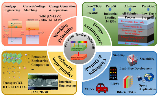
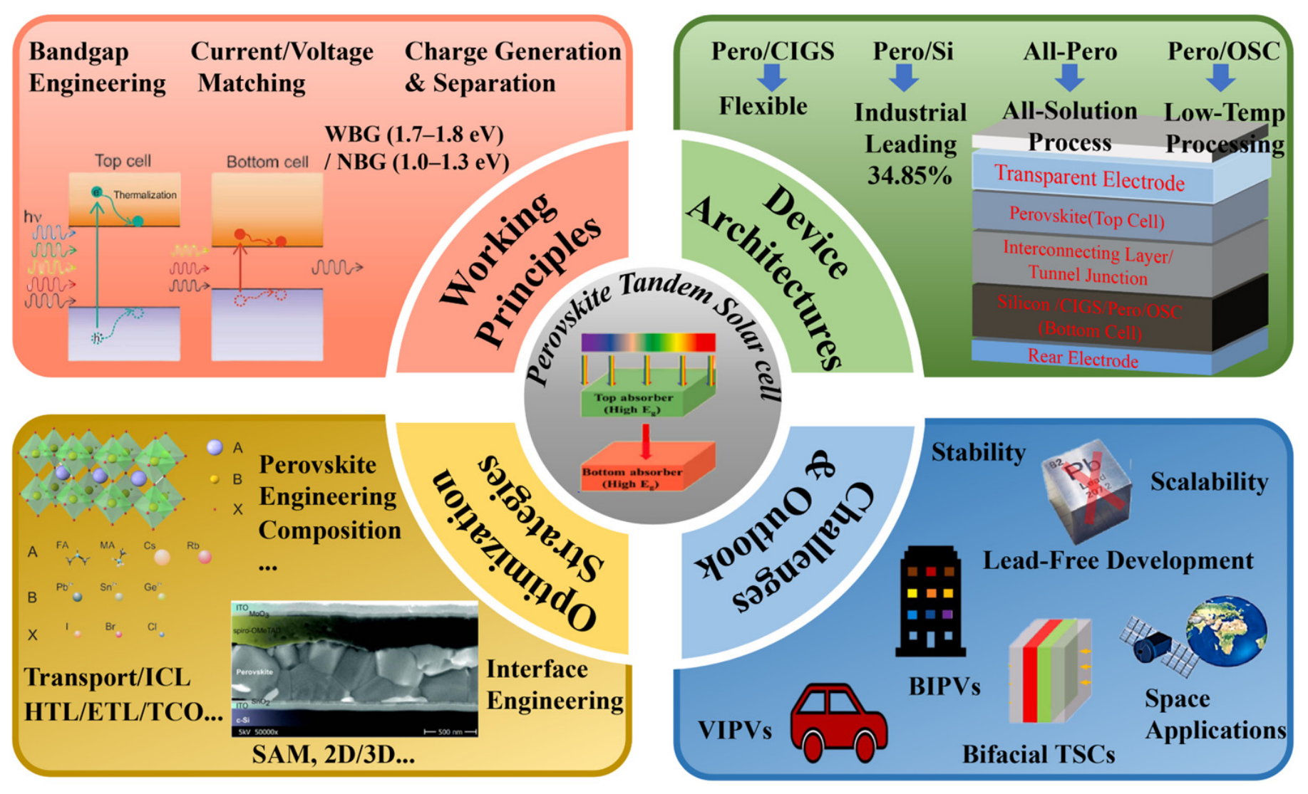
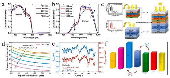
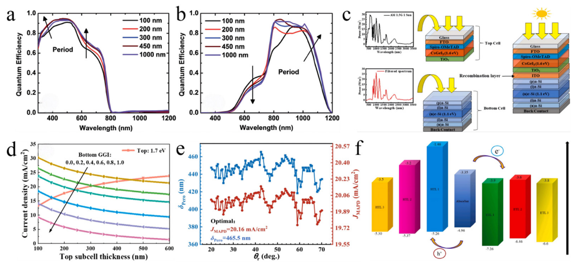

Disclaimer/Publisher’s Note: The statements, opinions and data contained in all publications are solely those of the individual author(s) and contributor(s) and not of MDPI and/or the editor(s). MDPI and/or the editor(s) disclaim responsibility for any injury to people or property resulting from any ideas, methods, instructions or products referred to in the content. |
© 2026 by the authors. Licensee MDPI, Basel, Switzerland. This article is an open access article distributed under the terms and conditions of the Creative Commons Attribution (CC BY) license.