
Article

Full Bridge LLC Hybrid Control Strategy with Wide Input and Output Voltage Range

1
School of Mechanical, Electrical & Information Engineering, Shandong University, Weihai 264209, China
2
WindSun (Qingdao) Transportation Technology Co., Ltd., Qingdao 266109, China
3
School of Electromechanical and Automotive Engineering, Yantai University, Yantai 264003, China
4
School of Future Technology, Shandong University, Jinan 250002, China
*
Authors to whom correspondence should be addressed.
Energies 2026, 19(13), 3051; https://doi.org/10.3390/en19133051
Submission received: 22 April 2026 / Revised: 7 June 2026 / Accepted: 25 June 2026 / Published: 27 June 2026
(This article belongs to the Special Issue Simulation, Stability, and Control in Inverter-Dominated Power Grids)

Abstract

The LLC resonant converter has gained extensive adoption in recent years, primarily owing to its benefits including high efficiency and high power density. However, the intrinsic electrical traits of the LLC converter fail to accommodate operational requirements involving a broad voltage span for both the input and the output. To tackle the operational scenarios of LLC resonant converters characterized by broad input and output voltage ranges, this study examines the gain properties of LLC subjected to both frequency modulation control and phase shift control techniques, correspondingly, and puts forward a hybrid control approach integrating frequency modulation with phase shift strategy. Through the seamless combination of frequency modulation control and phase shift control within one control loop, the issue of system oscillations occurring during the transition among differing control loops is successfully eliminated. As a result, the voltage gain spectrum of the LLC is substantially widened. A high-power LLC simulation model featuring interleaved and parallel configurations, along with an experimental testing rig, were established. The presented hybrid control strategy, which utilizes frequency modulation and phase shift, was investigated via extensive simulations and empirical testing. The obtained simulation results and experimental data exhibit strong alignment, thereby confirming the accuracy and feasibility of the presented full-bridge LLC hybrid control approach designed for extensive input and output voltage variations.

1. Introduction

LLC resonant converters, prized for their high efficiency and high power density characteristics, enjoy broad deployment in isolated DC–DC applications [1,2,3,4,5]. Although LLC resonant converters often rely on frequency modulation control, isolated DC–DC applications currently face an increasing demand for a broader input and output voltage range, which simple frequency modulation control alone can no longer satisfy over a wide range [6,7,8,9].
To meet the application demands for an extensive input–output voltage span, references [10,11] developed four distinct gain range operational modes utilizing primary-side half-bridge and full-bridge inverter switching, along with secondary-side bridge and voltage-doubling rectifier switching, thus attaining an ultra-wide output voltage range for the LLC. However, this circuit topology is intricate and hinders high-power scalability. References [12,13] attained a broad voltage range output for the LLC converter by incorporating resonant devices to alter the conventional resonant topology, although this approach resulted in elevated hardware expenses. References [14,15,16] employed PWM control or phase-shift control strategies for the LLC resonant converter, yet they failed to realize a seamless transition when switching to frequency modulation control and proved inadequate for applications demanding both wide input and output voltage ranges. References [17,18,19,20] altered the configuration of the resonant cavity by raising the quantity of resonant elements to five, which not only expanded the voltage gain characteristics but also enhanced efficiency. However, this addition of resonant elements altered the resonant points and voltage gain characteristics accordingly, thereby rendering the transformer’s characteristic analysis process more intricate.
This work focuses on the operational requirements for a wide voltage range across both input and output. By examining the gain profiles of the LLC under both frequency modulation and phase-shift control, a hybrid control scheme merging these two techniques is introduced. Through the normalization handling of control variables and the tuning of monotonicity, the adjustment spans of the two variables are effectively coupled. This integration merges both control methods into a single unified loop, which not only extends the LLC’s gain range but also eliminates system oscillation issues typically encountered during transitions between different loops. The proposed hybrid strategy, combining frequency and phase modulation, was simulated and experimentally validated on a high-power LLC interleaved and parallel model alongside a corresponding experimental platform. The simulation outcomes and experimental data exhibited strong agreement, thus confirming the validity and efficiency of the introduced full-bridge LLC hybrid control approach tailored for extensive input and output voltage ranges.

2. Input–Output Wide Voltage Range Hybrid Control Strategy

2.1. Frequency Control

2.1.1. Frequency Modulation Control Working Principle

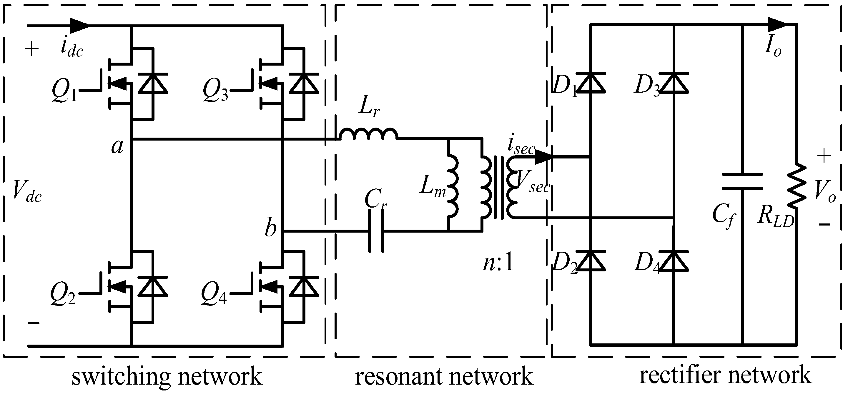
The structural configuration of the full-bridge LLC resonant converter is illustrated in Figure 1. Because the resonant portion of this LLC topology comprises three distinct resonant elements, the circuit produces two unique resonant frequency points depending on its specific operational conditions: the frequency resulting from the interaction of resonant inductor Lr and resonant capacitor Cr defines the series resonant frequency, denoted as fr; conversely, when the excitation inductor Lm resonates jointly with Lr and Cr, this condition is recognized as the series-parallel resonant frequency, symbolized as fm. The mathematical formulas for these two frequencies are provided below.
f r = 1 2 π L r C r
f m = 1 2 π ( L r + L m ) C r
In the LLC main circuit, the switch tubes of the Q1/Q4 and Q2/Q3 pairs are turned on simultaneously, while Q1/Q2 and Q3/Q4 are complementarily turned on. At this point, by controlling the switching frequency fs of the switch tubes, the LLC resonant circuit can operate at different resonant frequencies to achieve outputs with varying gains.

2.1.2. Gain Characteristics of LLC Under Frequency Modulation Control

To determine the voltage transfer relationship between the input and output of the LLC resonant converter, its structure can be broken down into three main sections: a switching network, a resonant network [21,22], and a rectification network. By using the fundamental component method to simplify and analyze each circuit network, the LLC input–output voltage effective value transmission ratio function M (fN) can be obtained [23,24,25,26]:
M ( f N , λ , Q ) = 1 ( 1 1 ( f N ) 2 ) Q f N 2 + ( 1 1 ( f N ) 2 ) 1 λ + 1 2
In Equation (3), fN represents the nominal frequency, which is:
f N = f s f r
Here, fs represents the actual operating resonant frequency of the LLC, while fr represents the theoretical resonant frequency of the LLC.
In Equation (3), λ represents the ratio of the excitation inductance to the resonant inductance; that is,
λ = L m L r
In Equation (3), Q represents the quality factor of the resonant circuit, and its expression is:
Q = Z r R a c = L r C r R a c
Here, Rac represents the equivalent resistance value of the rear end of the LLC resonant network.
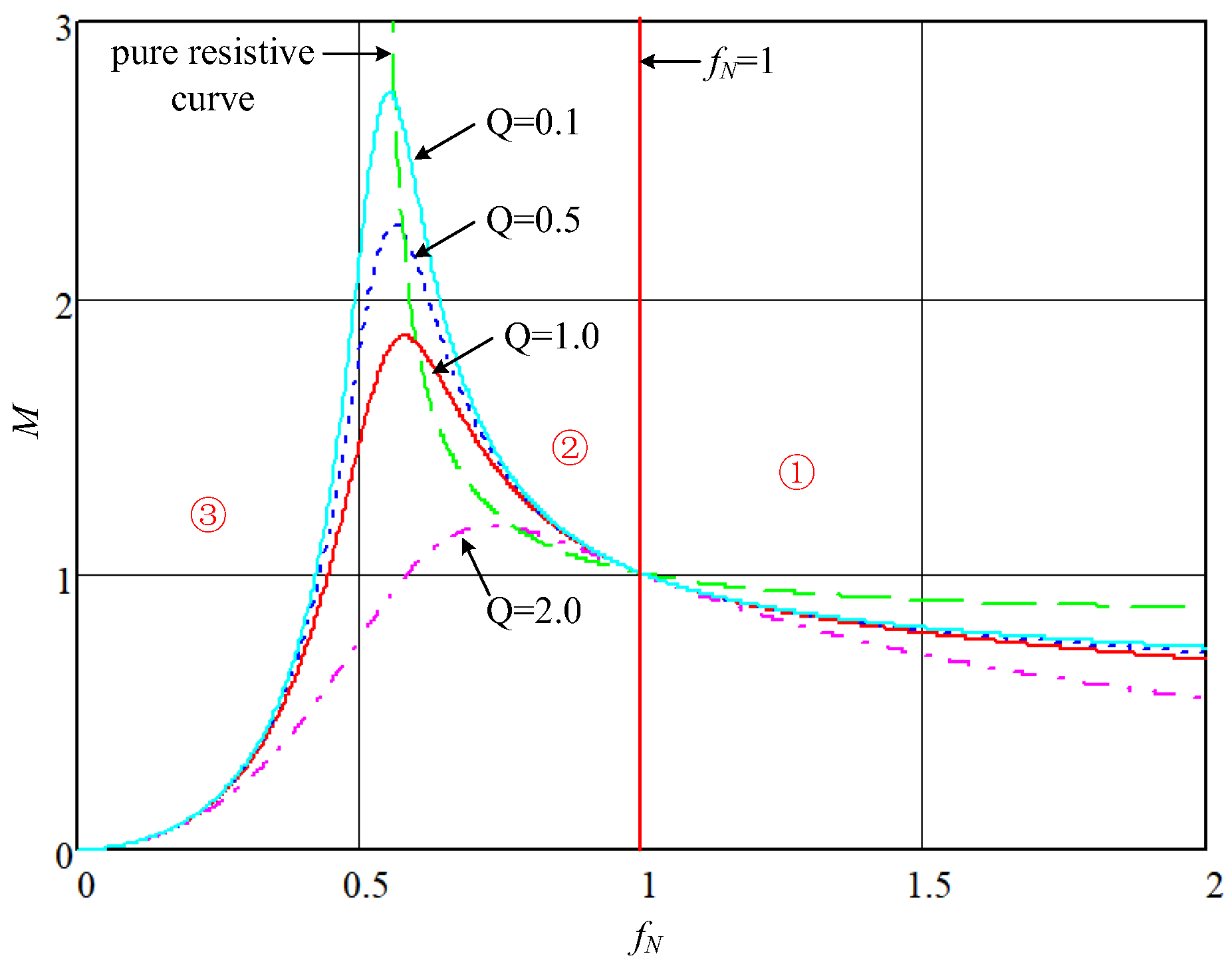
Setting λ = 3, the frequency-modulated gain characteristics of the LLC for various Q values can be determined using Equation (3), as illustrated in Figure 2.
From the LLC frequency gain curve shown above, it can be observed that, based on fN = 1 and the purely resistive curve, the LLC gain curve can be divided into three regions. To ensure that the LLC switch network operates in ZVS (Zero Voltage Switching) state and the rectifier network operates in ZCS (Zero Current Switching) state, the LLC resonant frequency must be controlled to operate in region 2, where the LLC is in boost mode.

2.2. Phase Control

2.2.1. The Working Principle of Phase Control

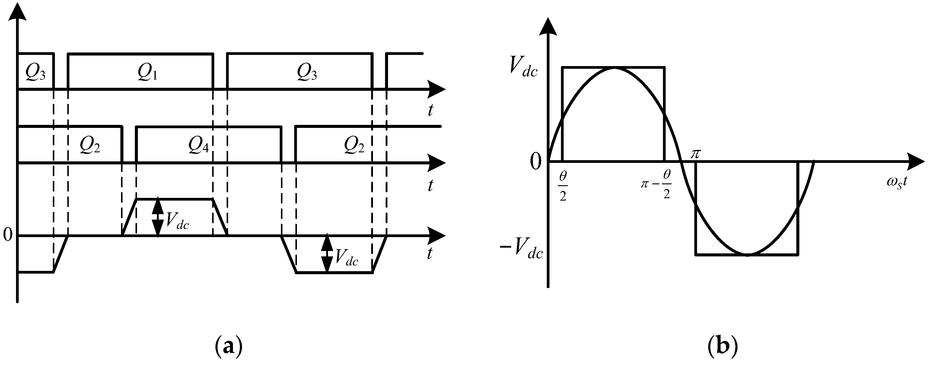
Phase shift control implies that when the LLC is running at a specific resonant frequency, the gate drive signals for Q1 and Q4, as well as those for Q2 and Q3, no longer operate simultaneously. Instead, a phase difference θ is introduced. By varying the value of this phase shift angle θ, the duty ratio of the bridge arm voltage vab can be modified, thereby enabling the regulation of the LLC gain [27,28,29,30]. The associated driving waveform for this control method is presented in Figure 3a.

2.2.2. Gain Characteristics of LLC Under Phase-Shift Control

When the LLC is operating under phase shift control, the switching network’s output voltage vab appears as a square wave featuring a duty cycle below 50%, as illustrated in Figure 3b.
In a similar vein, by applying Fourier series decomposition to vab and extracting the RMS value of its fundamental harmonic component, the fundamental voltage VabCF1 can be obtained as:
V a b C F 1 = 4 V d c cos ( θ / 2 ) π
In contrast to the fundamental harmonic of the frequency modulation mode, the fundamental component in the phase-shift operating mode is reduced by a factor of cos ( θ / 2 ) . Accordingly, one can derive that, when the LLC operates in the phase-shift mode, the expression for the input-to-output voltage ratio function MCF(fN) is given by:
M C F ( f N , λ , Q ) = cos ( θ / 2 ) ( 1 1 ( f N ) 2 ) Q f N 2 + ( 1 1 ( f N ) 2 ) 1 λ + 1 2
When the LLC is at the resonant frequency, fN equals 1, at which point the input–output voltage transmission ratio function MCF(fN) under the phase shifting mode is simplified to [31,32]:
M C F ( f N = 1 ) = cos ( θ / 2 )
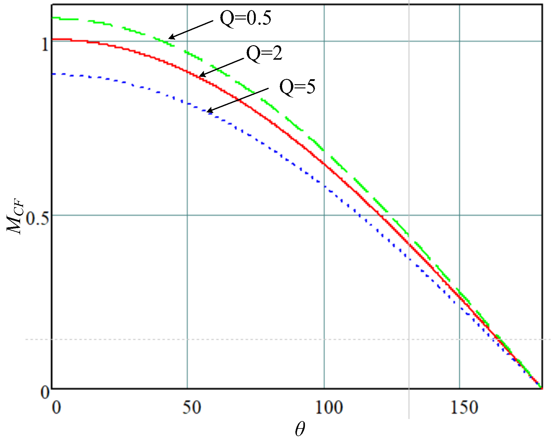
Based on Equation (9), the LLC phase-shift gain curve is shown in Figure 4 below.
As illustrated by the LLC phase-shifting gain curve in the figure above, a progressive rise in the phase shift angle θ corresponds to a continuous reduction in the LLC’s output gain, eventually reaching zero, at which point the converter enters buck mode.

2.3. Mixed-Control Strategy

When the LLC is in frequency modulation control mode, the ideal working condition is to operate in the under-resonance boosting zone of region 2. However, to widen the voltage operating range, it needs to be controlled in order to enter the over-resonance bucking zone of region 1. However, the operating frequency in region 1 is relatively high, the gain curve is flatter, it is not very sensitive to frequency changes, and it is also prone to operational oscillation problems due to the influence of parasitic parameters. Therefore, operating the LLC in region 1 does not resolve the issue of a wide input–output voltage range for the LLC.
LLC phase-shift control is capable of lowering the voltage gain, thereby offsetting the drawbacks associated with operation in the over-resonance region under frequency modulation control. Consequently, to satisfy the input–output wide voltage range operational demands of the LLC, LLC frequency modulation control and phase-shift control are integrated in this study to develop a hybrid control strategy combining both frequency modulation and phase shift. The detailed procedure is outlined as follows:
Define the control strategies for both the LLC frequency modulation and phase shift.
To guarantee the stable operation of the LLC, both approaches employ a dual closed-loop control strategy incorporating voltage and current regulation. The schematic diagram for the LLC frequency modulation control strategy is presented in Figure 5a, while the corresponding diagram for the phase-shift control strategy is given in Figure 5b.
Perform normalization on the control variables.
Given that the LLC operates most efficiently at its resonant frequency, this specific frequency is adopted as the transition point between frequency modulation control and phase-shift control when normalizing the control variable.
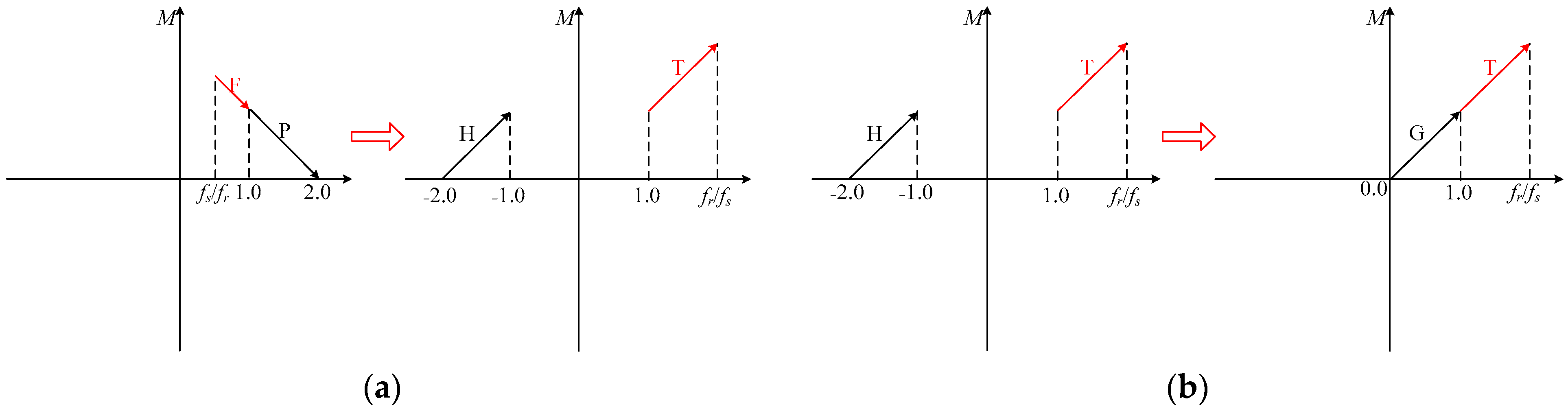
Regarding the frequency modulation control parameter, let the LLC resonant frequency be fr and its modulation range be fsfr. The normalized frequency modulation range FF, derived by taking fr as the reference, is expressed as fs/fr–1.0.
Concerning the phase-shift control parameter, the practical realization of phase-shift control relies on the phase of Q1 and utilizes Q3 to regulate the phase shift angle. The starting phase shift value of Q3 is set to 180 degrees, and the phase shift range extends from 180 degrees to 360 degrees. Consequently, after scaling the control signal based on 180 degrees, the phase shift range P falls between 1.0 and 2.0.
Tune both the frequency modulation and phase shift control approaches to guarantee that the two gain profiles exhibit identical monotonic characteristics.
In actual control systems, the control chip achieves dynamic frequency modulation control by adjusting the count value when constructing the carrier wave. The difference in count values reflects different period values, so LLC frequency modulation control essentially adjusts the size of the period value directly. At this time, the gain of the LLC device changes from a decreasing characteristic that lowers with the modulation control amount to an increasing characteristic that rises with the period control amount. Since the LLC period value is the reciprocal of the frequency value, the controller’s output control range changes from F: fs/fr–1.0 to T: 1.0–fr/fs.
To guarantee that the phase-shift control and the modified frequency modulation control exhibit identical gain monotonicity, the phase-shift control loop must be inverted. Specifically, the normalized range of the output phase-shift control variable shifts from P: 1.0–2.0 to H: −2.0~−1.0. Consequently, the gain of the LLC device transitions from a decreasing characteristic, where the gain drops as the phase-shift control variable increases, to an increasing characteristic, where the gain rises along with the phase-shift control variable. The tuning procedure for both the frequency modulation control variable and the phase-shift control variable is illustrated in Figure 6a.
Integrated control loop combining frequency modulation and phase-shift control
Once the gain of the frequency modulation control and that of the phase-shift control share the same monotonic trend, the two individual control loops can be unified into a single frequency modulation-phase shift control loop, which utilizes a common PI controller for output regulation. This arrangement facilitates a seamless transition between the frequency modulation control strategy and the phase-shift control strategy, thereby preventing oscillation problems in the DC voltage.
Under frequency modulation control, when T changes from 1.0 to fr/fs, the gain of the LLC device increases monotonically, but the gain value is not zero within its operating range; under phase shift control, when H changes from −2.0 to −1.0, the gain of the LLC device also increases monotonically, and begins to change from zero. Considering that the PI controller’s adjustment process also starts from zero and then gradually changes, it is necessary to convert the output of the phase shift control again. Its output per unit value changes from H: −2.0 to −1.0, increasing by 2.0 to become G: 0.0 to 1.0, which aligns perfectly with the frequency modulation control range of 1.0 to fr/fs, forming the overall frequency modulation phase shift control range Y: 0.0 to fr/fs. This ensures that, during the establishment of the frequency modulation phase shift control loop, the overall gain of the LLC is first increased through phase shift control. If the gain is insufficient, the closed-loop control output Y automatically transitions from 0.0 to 1.0 to 1.0 to 2.0 for frequency modulation control to further increase the overall gain of the device until the control target is achieved. The LLC frequency modulation phase shift mixed-control strategy not only achieves a wide voltage range gain for LLC input and output but also ensures that the LLC gain starts from zero, accommodating the LLC soft start process. The process of merging LLC frequency modulation and phase shift control is shown in Figure 6b.
Based on the output of the frequency modulation phase control loop, restore the frequency modulation value and the phase shift value.
The output of the frequency modulation phase control loop is only a control quantity Y: 0.0–fr/fs, but it actually contains two control parameters: the frequency modulation value T and the phase shift value p. Therefore, it is necessary to distinguish between them to facilitate the final control. The frequency modulation phase control range of 0.0–1.0 is actually the phase shift control interval. When it is determined that the controller output is less than 1.0, the original phase shift per unit value p: 1.0–2.0 can be adjusted using the formula 2.0–Y; the frequency modulation phase control range of 1.0–fr/fs is actually the frequency modulation control interval. When it is determined that the controller output is greater than 1.0, the control quantity remains unchanged, which corresponds to restoring the frequency modulation per unit value T: 1.0–fr/fs. Based on the obtained frequency modulation value T and phase shift value p per unit, by restoring to the final actual frequency modulation phase values, the control of the LLC DC power supply device can be achieved. The block diagram for restoring the LLC frequency modulation value and phase shift value control is shown in Figure 7.

3. Simulation Research

The simulation model for the LLC was constructed within the Matlab 2018a environment, with its main circuit structure depicted in Figure 1. Detailed simulation parameters are listed in Table 1.
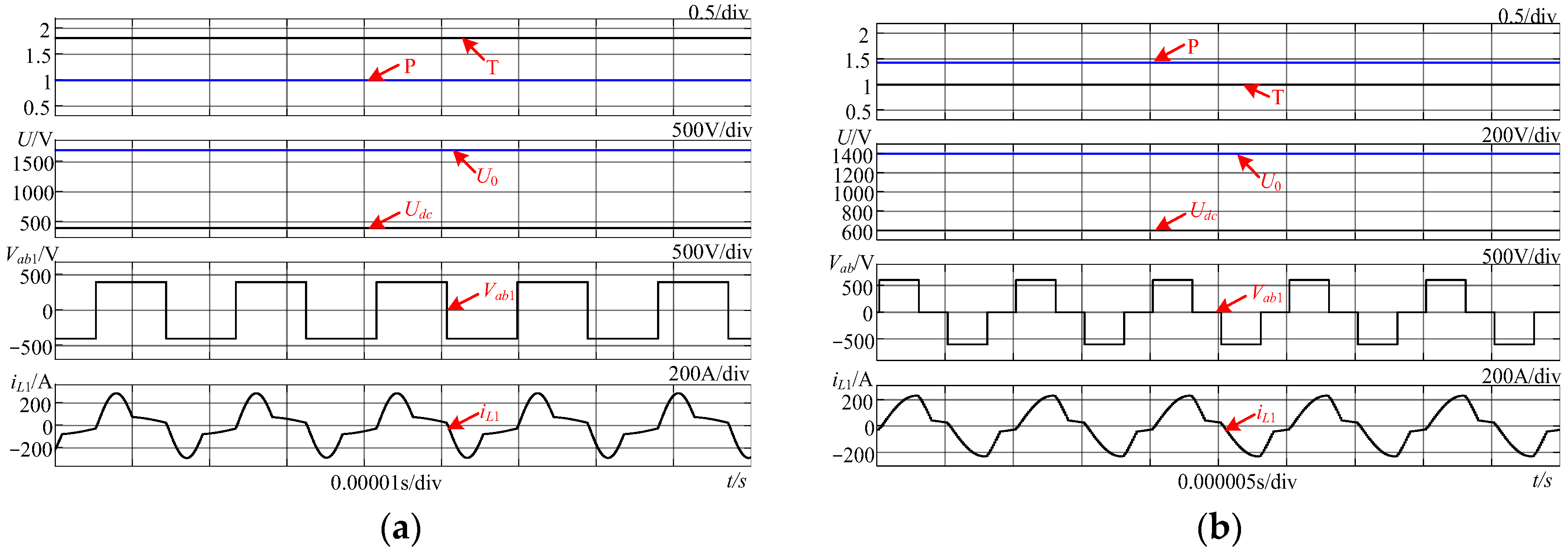
For an input voltage of 400 V and a regulated output voltage of 1700 V, assess the rated power operation of the LLC under low-input and high-voltage-boost conditions. The corresponding simulation waveform is displayed in Figure 8a.
The simulation data depicted above reveals that, under the LLC’s step-up operation from a low input voltage to a high output voltage, the per-unit phase shift control variable p maintained a value of 1, whereas the per-unit frequency control variable T consistently exceeded 1, which signifies that the LLC functions in a sub-resonant state under frequency control; it is capable of regulating the peak output voltage at the minimum input voltage while supporting full-load operation, thereby demonstrating that the gain during the boost phase satisfies the specifications over the entire operational range.
With a 600 V input and a targeted output voltage of 1400 V, the nominal power operational performance of the LLC when subjected to a high input voltage and a low output voltage was evaluated. The corresponding simulation waveform is depicted in Figure 8b.
From the simulation results in the above figure, it can be seen that, under the condition of high voltage input and low voltage output step-down, the frequency modulation control quantity marked by the per unit value T was always 1, and the phase-shifting control quantity marked by the per unit value p was always greater than 1, indicating that the LLC operates in phase-shifting control mode; the LLC can control the lowest output voltage value at full load under the highest input voltage, indicating that its step-down gain meets requirements across the entire range.
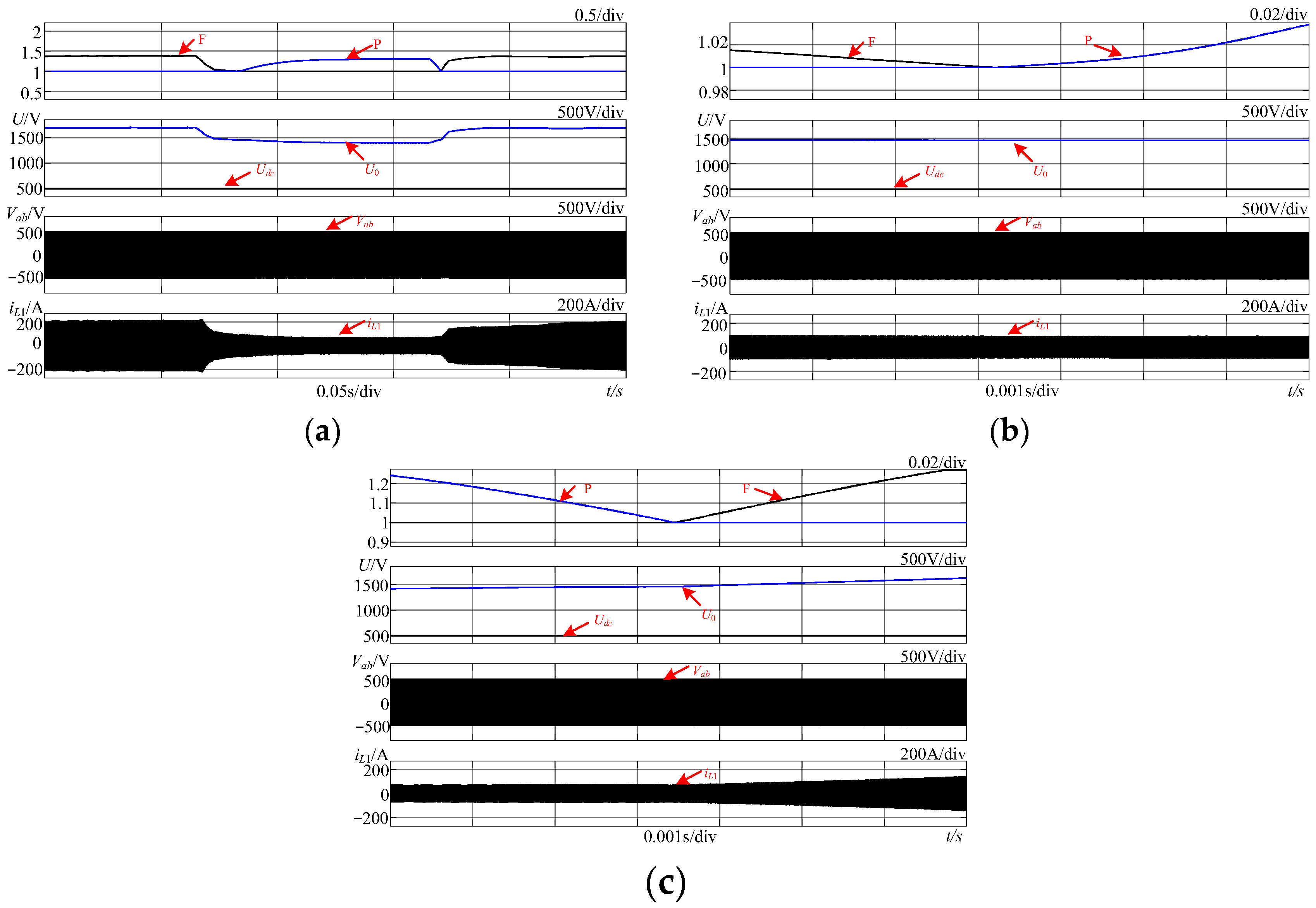
With an input voltage of 500 V, the output voltage was dynamically switched from 1700 V to 1400 V and then back to 1700 V, testing the dynamic smooth switching process of the LLC hybrid control strategy under different gain outputs, as shown in the simulation waveforms in Figure 9.
The simulation findings presented in the figure above demonstrate that, during multiple transitions of the LLC’s output voltage target value, neither the foundational basis for the frequency modulation and phase shift control strategies nor the hysteresis magnitude need to be adjusted. The LLC can automatically achieve smooth and seamless switching based on the LLC output gain requirement through its own controller adjustment, and there are no system oscillation issues during the switching process, thus meeting the design requirements.

4. Experimental Research

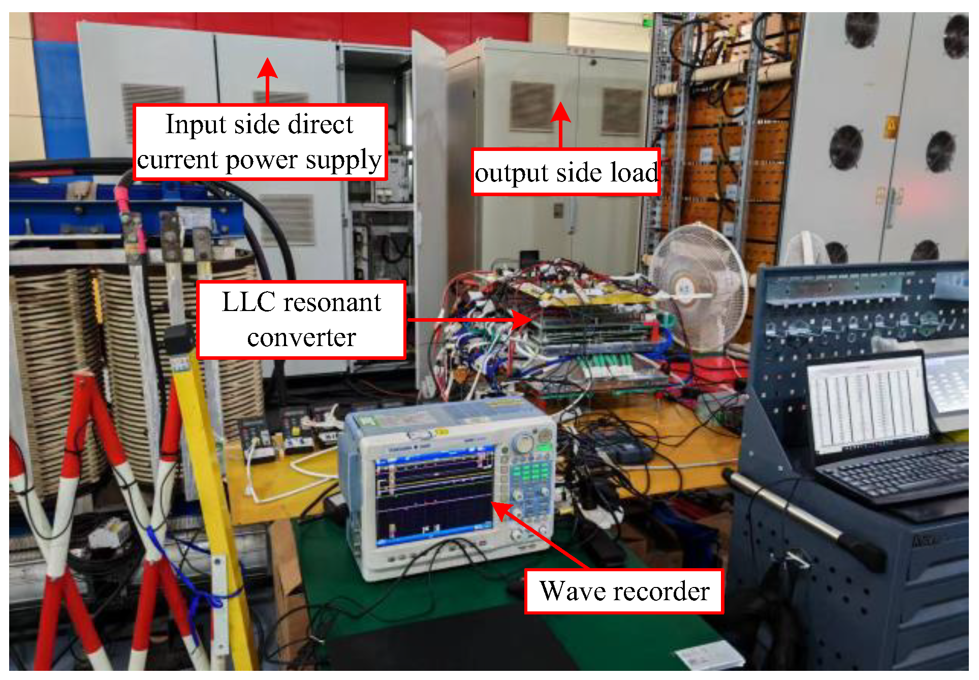
To further validate the accuracy and efficacy of the wide-voltage-range hybrid control strategy for the input and output, the experimental hardware platform (presented in Figure 10) was constructed based on the LLC main circuit topology shown in Figure 1. Relevant experimental investigations were conducted on this testing setup, and the specifications of the experimental system were consistent with those used in the simulation model.
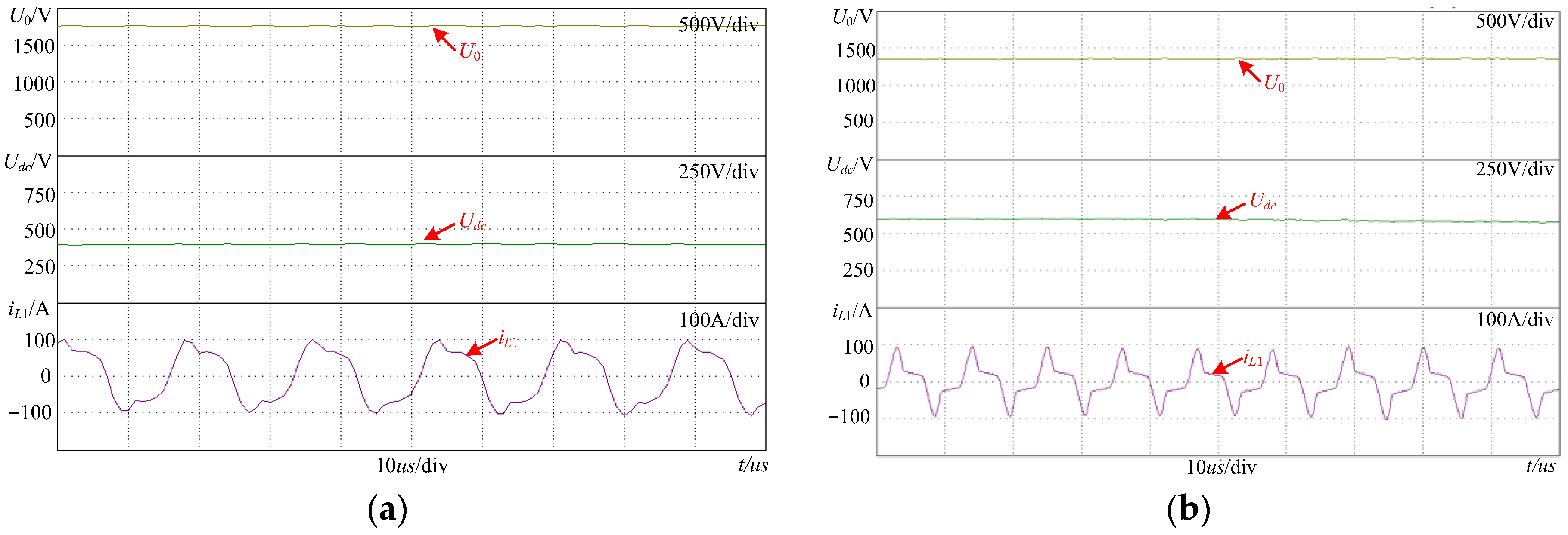
With an input voltage of 400 V and a regulated output voltage of 1700 V, the operational performance of the LLC was evaluated under step-up conditions characterized by a low input voltage and a high output voltage. The corresponding experimental waveform is presented in Figure 11a.
The experimental results shown in the above figure indicate that the LLC operated within the frequency modulation range and functioned normally under low voltage input and high voltage output boost conditions. This demonstrates that the gain for the boost conditions meets the requirements across the entire range, with the simulation results aligning with the experimental findings.
The operational status of the LLC under high input voltage and low output voltage buck operating mode was evaluated, with the specific experimental waveforms displayed in Figure 11b.
The experimental findings presented above reveal that, under the condition of a high input voltage and low output voltage for step-down applications, the LLC functioned normally within its phase-shifted range while supporting a load. This indicates that the gain performance satisfies the specifications across the full range for the step-down scenario, and the simulation outcomes are consistent with the experimental measurements.
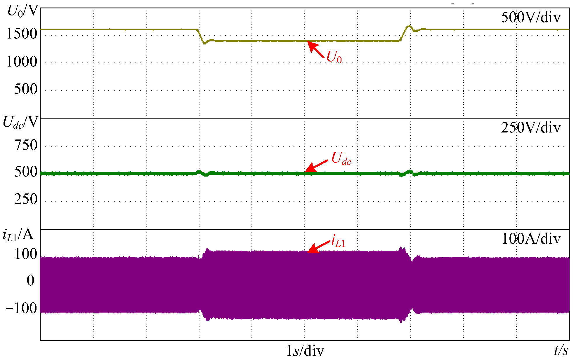
With an input voltage set to 500 V, the output voltage was regulated to dynamically transition from 1600 V to 1400 V and then back to 1600 V. The validation of the LLC hybrid control strategy during this dynamic and seamless switching procedure under varying gain outputs is illustrated in the waveform shown in Figure 12.
From the experimental results in the above figure, it can be seen that, during the multiple switching processes of the output voltage target value, the frequency modulation control and phase-shifting control automatically achieved smooth and seamless switching through their own controllers according to the gain requirements of LLC without causing system oscillation issues, thus meeting the design requirements.

5. Conclusions

To tackle the challenge of operating the LLC across a broad input and output voltage range, this study presents a combined control approach that integrates frequency modulation and phase shifting to manage the gain characteristics of the LLC under these respective control methods. Through the normalization of control variables and the tuning of their monotonic behavior, the adjustment ranges of the frequency modulation variable and the phase shifting variable are made interdependent, which effectively unifies these two control schemes into a single control loop. This integration not only extends the LLC’s gain range but also prevents system oscillation issues during transitions between distinct control loops. The effectiveness of the proposed approach was verified through both simulation and experimental testing on a high-power LLC interleaved and parallel simulation model and experimental platform. The following conclusions can be drawn:
(1)
The proposed frequency modulation and phase shifting mixed-control strategy can ensure that LLC operates stably within the wide voltage range for input and output applications, verifying the correctness and effectiveness of the input and output wide-voltage-range LLC hybrid control strategy proposed in this paper.
(2)
To broaden the input and output voltage range of the LLC, this paper introduces phase-shifting control, which will inevitably lead to a decrease in the overall efficiency of the LLC.
(3)
In subsequent research, it is necessary for us to find a more effective control method that can expand the input and output voltage range of the LLC without affecting the efficiency of the entire machine.

Author Contributions

J.W.: Writing-review & editing, Writing-original draft, Visualization, Investigation. L.W.: Writing-review & editing, Supervision, Project administration, Funding acquisition. C.L.: Writing-review & editing, Formal analysis. T.L.: Writing-review & editing, Visualization. M.J.: Writing-review & editing, Formal analysis. G.S.: Writing-review & editing, Supervision, Formal analysis. All authors have read and agreed to the published version of the manuscript.

Funding

This work was supported by the Key R&D Program of Shandong Province, China (2023CXGC010204), the National Natural Science Foundation of China (Grant No. 62403278) and the Natural Science Foundation of Shandong Province (Grant No. ZR2024QE180).

Data Availability Statement

The data presented in this study are available on request from the corresponding author due to privacy reasons.

Conflicts of Interest

Author Jianhua Wu was employed by the company WindSun (Qingdao) Transportation Technology Co., Ltd. Author Chuanduo Liu was employed by the company WindSun (Qingdao) Transportation Technology Co., Ltd. Author Maisheng Ji was employed by the company WindSun (Qingdao) Transportation Technology Co., Ltd. The remaining authors declare that the research was conducted in the absence of any commercial or financial relationships that could be construed as a potential conflict of interest.

References

  1. Park, M.-H.; Jeong, Y.; Rorrer, R.A.L.; Choi, D.; Moon, G.-W. Hold-up Time Extension Method for LLC Resonant Converter by Detecting Operation Region. IEEE Trans. Power Electron. 2020, 35, 9949–9952. [Google Scholar] [CrossRef]
  2. Mishima, T.; Mizutani, H.; Nakaoka, M. A Sensitivity-Improved PFM LLC Resonant Full-Bridge DC-DC Converter with LC Antiresonant Circuitry. IEEE Trans. Power Electron. 2016, 32, 310–324. [Google Scholar]
  3. Liu, C.; Xu, X.; He, D.; Liu, H.; Tian, X.; Guo, Y.; Cai, G.; Ma, C.; Mu, G. Magnetic-Coupling Current-Balancing Cells Based Input-Parallel Output-Parallel LLC Resonant Converter Modules for High-Frequency Isolation of DC Distribution Systems. IEEE Trans. Power Electron. 2016, 31, 6968–6979. [Google Scholar]
  4. Jeong, Y.; Lee, M.-S.; Park, J.-D.; Kim, J.-K.; Rorrer, R.A.L. Hold-up Time Compensation Circuit of Half-Bridge LLC Resonant Converter for High Light-load Efficiency. IEEE Trans. Power Electron. 2020, 35, 13126–13135. [Google Scholar] [CrossRef]
  5. Wen, H.; Gong, J.; Zhao, X.; Yeh, C.-S.; Lai, J.-S. Analysis of Diode Reverse Recovery Effect on ZVS Condition for GaN-Based LLC Resonant Converter. IEEE Trans. Power Electron. 2019, 34, 11952–11963. [Google Scholar]
  6. Tang, X.; Wu, H.; Zhao, J.; Xing, Y. Family of Half-Bridge LLC Resonant Converters with Auxiliary Switches for Hold-Up Operation. IET Power Electron. 2019, 12, 1376–1384. [Google Scholar]
  7. Qinglin, Z.; Dong, G.; Da, Z.; Deyu, W.; Yi, Z. Three-phase Multi-resonant Converter with Wide-output-voltage Range. Power Syst. Technol. 2022, 46, 4085–4094. (In Chinese) [Google Scholar] [CrossRef]
  8. Xiqi, W.; Rui, L.; Xu, C.; Wei, Y. A New Wide Voltage Gain DC Charging Module Topology and Modulation Technology. Proc. CSEE 2021, 41, 8129–8139. (In Chinese) [Google Scholar] [CrossRef]
  9. Yu, Z.; Wu, H.; Hua, W.; Xing, Y. A LLC Resonant Converter with Matrix-transformer and Phase-shift Control for Wide Voltage Range Applications. Proc. CSEE 2019, 39, 3638–3646. (In Chinese) [Google Scholar] [CrossRef]
  10. Zhang, J.; Lin, G. A Variable-Mode Ultra-Wide Output Voltage Gain Dual LLC Resonant Converter and Control Method. Trans. China Electrotech. Soc. 2025, 40, 8052–8065+8079. (In Chinese) [Google Scholar] [CrossRef]
  11. Sun, X.Y.; Deng, Y.H.; Nie, J.L.; Ma, L.; Shu, Z.L. An Ultrawide Voltage Gain Dual LLC Resonant Converter and Control Method. Proc. CSEE 2024, 44, 1974–1985. (In Chinese) [Google Scholar] [CrossRef]
  12. Qin, Y.; Ren, C.; Kong, J.; Zhang, B.; Han, X. DC-DC Converter with Wide Input Voltage Range Based on Multi-resonant Structure. J. Power Supply 2025, 23, 26–34. (In Chinese) [Google Scholar] [CrossRef]
  13. Duan, S.; Han, Y.; Li, J.; Zhao, Z.; Liu, H. Wide-voltage Hybrid Bridge Bidirectional DC-DC Converter. J. Power Supply 2026, 24, 19–26. (In Chinese) [Google Scholar] [CrossRef]
  14. Khan, S.; Sha, D.; Jia, X.; Wang, S. Resonant LLC DC-DC converter employing fixed switching frequency based on dual-transformer with wide input-voltage range. IEEE Trans. Power Electron. 2020, 36, 607–616. [Google Scholar]
  15. Wang, H.; Li, Z. A PWM LLC type resonant converter adapted to wide output range in PEV charging applications. IEEE Trans. Power Electron. 2018, 33, 3791–3801. [Google Scholar]
  16. Shang, M.; Wang, H. A voltage quadrupler rectifier based pulse width modulated LLC converter with wide output range. IEEE Trans. Ind. Appl. 2018, 54, 6159–6168. [Google Scholar] [CrossRef]
  17. Fu, D. Topology Investigation and System Optimization of Resonant Converter. Ph.D. Thesis, Virginia Polytechnic Institute and State University, Blacksburg, VA, USA, 2010. [Google Scholar]
  18. Zhang, X.; Jing, J.; Guan, Y.; Dai, M.; Wang, Y.; Xu, D. High-efficiency high-order CL-LLC dc/dc converter with wide input voltage range. IEEE Trans. Power Electron. 2021, 36, 10383–10394. [Google Scholar]
  19. Zhao, Q.; Liu, W.; Wang, Y.; Wang, D.; Wu, N. A novel multiresonant DC-DC converter with wide output-voltage range. IEEE Trans. Power Electron. 2019, 35, 5625–5638. [Google Scholar]
  20. Wu, H.; Jin, X.; Hu, H.; Xing, Y. Multielement resonant converters with a notch filter on secondary side. IEEE Trans. Power Electron. 2015, 31, 3999–4004. [Google Scholar] [CrossRef]
  21. Zhou, Y.; Sheng, L.; Wang, Y. CLL Resonant Converter for Variable Inductance Applications. Power Electron. 2020, 54, 10–14. (In Chinese) [Google Scholar]
  22. Lin, R.L.; Lin, C.W. Design Criteria for Resonant Tank of LLC DC-DC Resonant Converter. In Proceedings of the IECON 2010-36th Annual Conference on IEEE Industrial Electronics Society, Glendale, AZ, USA, 7–10 November 2010. [Google Scholar]
  23. Sheng, L.; Zhou, Y.; Wu, Q. Analysis and Design of Non-isolated LLC Resonant Converter. Electr. Drive 2021, 51, 33–39. (In Chinese) [Google Scholar] [CrossRef]
  24. Chen, Z.; Chen, K.; Xiong, X.; He, R. Variable frequency interleaved parallel LLC resonant converter based on variable inductor. Electr. Mach. Control. 2020, 24, 97–105. (In Chinese) [Google Scholar] [CrossRef]
  25. Li, J.; Ren, X.; Zhou, Z.; Zhang, Z.; Chen, Q. Research on Current Sharing Optimization of Bidirectional LLC-DCX Multi-Module Parallel System Based on Resonant Network Optimization. Trans. China Electrotech. Soc. 2023, 38, 2720–2730+2756. (In Chinese) [Google Scholar] [CrossRef]
  26. Zhu, X.; Liu, K.; Ye, K.; Jiang, L.; Jin, K. Isolated Bidirectional Hybrid LLC Converter Based on SiC MOSFET. Trans. China Electrotech. Soc. 2022, 37, 4143–4154. (In Chinese) [Google Scholar] [CrossRef]
  27. Koji, M.; Fujio, K. A novel interleaved LLC resonant converter with phase shift modulation. In Proceedings of the 2014 IEEE Energy Conversion Congress and Exposition (ECCE), Pittsburgh, PA, USA, 15–18 September 2014; pp. 2051–2056. [Google Scholar]
  28. Yu, Z.; Wu, H.; Hua, W.; Zhu, J.; Xing, Y. A dual-transformer-based LLC resonant converter with phase-shift control for hold-up time compensation application. In Proceedings of the 2018 IEEE Energy Conversion Congress and Exposition (ECCE), Vancouver, BC, Canada, 23–27 September 2018; IEEE: New York, NY, USA, 2018; pp. 5961–5966. [Google Scholar]
  29. Zhao, L.; Li, H.; Wu, X.; Zhang, J. An improved phase-shifted full-bridge converter with wide-range ZVS and reduced filter requirement. IEEE Trans. Ind. Electron. 2017, 65, 2167–2176. [Google Scholar]
  30. Liu, W.; Wang, B.; Yao, W.; Lu, Z.; Xu, X. Steady-state analysis of the phase shift modulated LLC resonant converter. In Proceedings of the 2016 IEEE Energy Conversion Congress and Exposition (ECCE), Milwaukee, WI, USA, 18–22 September 2016; IEEE: New York, NY, USA, 2016; pp. 1–5. [Google Scholar]
  31. Wang, D.; Li, Y.; Zhao, Q.; Li, J.; Zhang, D. Wide Output Range Multi-level LLC Resonant Converter with Fixed-frequency Phase-shift Control. Proc. CSEE 2023, 43, 1973–1984. (In Chinese) [Google Scholar] [CrossRef]
  32. Miao, Z.; Tong, H.; Yao, W.; Lu, Z. A Flexible Variable-mode Control Method for Wide-range Full-bridge LLC Converter. Proc. CSEE 2022, 42, 747–761. (In Chinese) [Google Scholar] [CrossRef]
Figure 1. Power circuit schematic of the full-bridge LLC resonant converter.
Energies 19 03051 g001
Figure 2. LLC frequency modulation gain curve.
Energies 19 03051 g002
Figure 3. Phase-shift control drive waveform (a) and phase-shift control lower bridge arm voltage waveform (b).
Energies 19 03051 g003
Figure 4. LLC phase-shift gain curve.
Energies 19 03051 g004
Figure 5. LLC Frequency Modulation Control Strategy Block Diagram (a) and LLC Phase Shift Control Strategy Block Diagram (b).
Energies 19 03051 g005
Figure 6. Tuning procedure for the control variables of both frequency modulation and phase shift (a) and Schematic illustrating the integration of LLC frequency modulation with phase-shift control (b).
Energies 19 03051 g006
Figure 7. Control block diagram for frequency modulation value and phase shift value restoration.
Energies 19 03051 g007
Figure 8. Low voltage input, high voltage output boost condition waveform diagram (a) and high voltage input, low voltage output buck condition waveform (b).
Energies 19 03051 g008
Figure 9. Waveform of the dynamic transition process of the LLC hybrid control strategy (a), waveform for the transition from frequency modulation control to phase-shift control (b), and waveform for the transition from phase-shift control to frequency modulation control (c).
Energies 19 03051 g009
Figure 10. Photograph of the experimental hardware platform.
Energies 19 03051 g010
Figure 11. Low voltage input, high voltage output boost condition waveform diagram (a) and high voltage input, low voltage output buck operating waveform (b).
Energies 19 03051 g011
Figure 12. Dynamic switching process waveform diagram of LLC mixed-control strategy.
Energies 19 03051 g012
Table 1. Simulation parameters.
Parameter NameValueParameter NameValue
Input voltage400–600 VResonant transformer
turns ratio
0.3
Output voltage1400–1700 VResonant inductor3.072 × 10−6 H
Resonant frequency100 kHzResonant capacitor8.246 × 10−7 F
Module power50 kWExcitation inductance9.215 × 10−6 H
Disclaimer/Publisher’s Note: The statements, opinions and data contained in all publications are solely those of the individual author(s) and contributor(s) and not of MDPI and/or the editor(s). MDPI and/or the editor(s) disclaim responsibility for any injury to people or property resulting from any ideas, methods, instructions or products referred to in the content.