


Abstract
Heterogeneous integration opens a pathway to three-dimensional chiplet-based microsystem chips. Electrostatic discharge reliability is a major challenge to future smart chips featuring rich functionalities and ultra performance, utilizing advanced heterogeneous integration and packaging technologies. This paper discusses emerging challenges and future research directions in developing robust electrostatic discharge protection solutions for future systems-on-integrated-chiplets.
1. Introduction
As Moore’s Law rapidly approaches its physical wall, a major question arises: what will future chips look like? Driven by the emerging transition from the information (IT) era to the Internet of Everything (IoET) age, the general answer is that smart future chips featuring vast functional diversity, extreme performance and good affordability are needed to enable the IT-to-IoET transition. It is generally agreed upon that heterogeneous integration (HI) technology opens the pathway to smart future chips. In principle, HI technologies can hetero-integrate different devices made with dissimilar materials, using various technologies at different nodes into systems-on-integrated-chiplets (SoICs) in an advanced micro-scale package (µ-package) to deliver the desired rich functionalities and ultra performance at low costs for future smart chips [1]. The IT era has been compute-centric and technology-driven, which encompasses traditional “IC functions” including signal processing, computing, storage and networking; all these hallmark operations are naturally suitable to and greatly benefiting from monolithic chips in Si CMOS. On the other hand, the IoET age will be more system-oriented and data-driven in order to handle complex technology–human–world interfaces, which relies on smart future chips with emerging “non-IC functions”, such as sensing, actuation, control, mechanical, photonic, quantum and bio-inspired functions better facilitated by 3D heterogeneous SoICs.
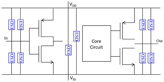
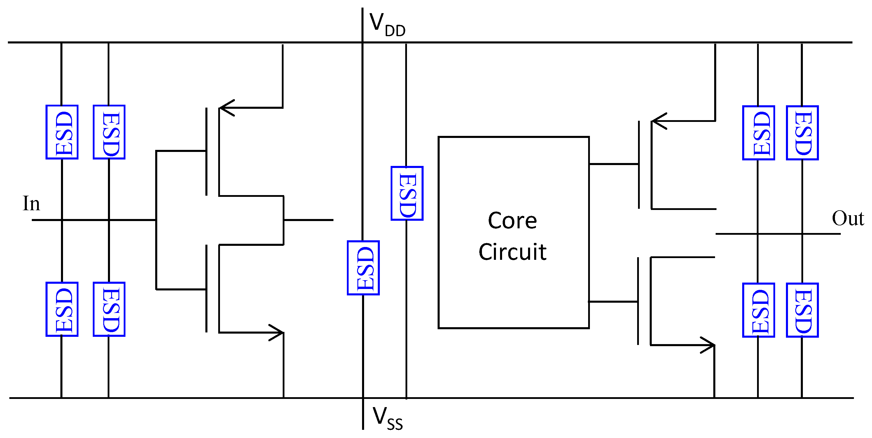
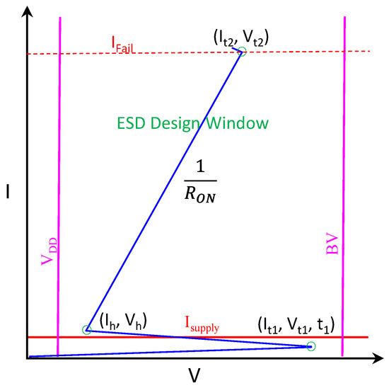
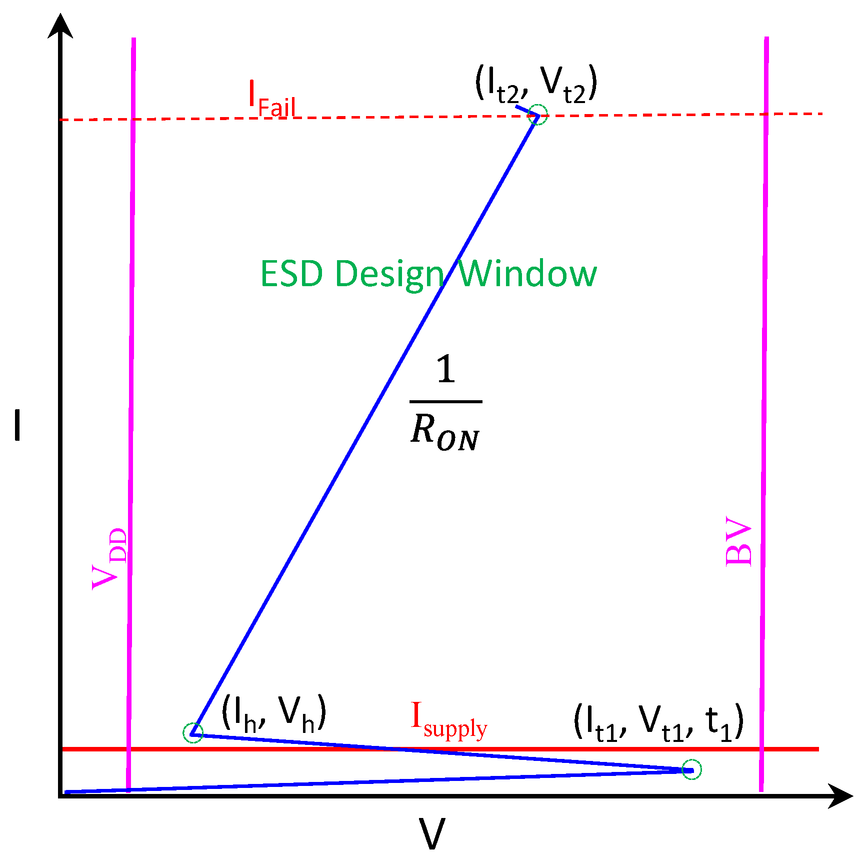
Reliability plays a key role in realizing 3D heterogeneous SoICs with µ-packaging in terms of being able to unlock the full potential for different devices made in their native material platforms for superior microsystem performance. Electrostatic discharge (ESD) failure emerges as a grand reliability challenge to SoICs due to their uniqueness, including functionalities, performance, physical complexities and lifetime, hence making ESD protection for SoICs much more challenging than on-chip ESD protection for monolithic chips. ESD occurs when two objects of different electric potentials are brought together; electrostatic discharge will start in between, producing very fast and strong transient voltage and current pulses, which can readily damage ICs [2,3,4,5]. Generally, on-chip ESD protection works in that ESD protection devices are placed at each pad, which stay Off during normal IC operations. If an external ESD pulse appears on an IC pad, the ESD device will be turned on swiftly to form a low-resistance conduction path to shunt the incoming ESD transient into the ground (GND), hence protecting the IC. As illustrated in Figure 1, full ESD protection requires a complete ESD discharging network on a chip [5]. Good on-chip ESD protection design requires careful consideration of the following key factors [6,7,8]. ESD-critical parameters must be accurately designed including ESD triggering voltage (Vt1), current (It1) and time (t1); holding voltage (Vh) and current (Ih); discharge resistance (RON), ESD failure voltage and current (Vt2, It2), etc. The ESD design window, depicted in Figure 2, must be complied with for every pad on a chip. ESD-induced design overhead effects must be minimized, including ESD-induced parasitic capacitance (CESD), noises, leakage and layout sizes. ESD-IC co-design is required for high-speed and RF ICs. ESD simulation and full-chip design verification are required for ESD design optimization and prediction. Indeed, these practical ESD protection considerations are very involving and complicated. Unfortunately, ESD protection will be much more challenging for 3D heterogeneous SoICs in advanced packages, which will be discussed in this paper.
Figure 1.
Illustration of full-chip ESD protection principle.
Figure 2.
Illustration of an ESD design window. Good ESD protection design requires all ESD-critical parameters to be within the ESD design window for a chip.
2. Emerging Challenges and Future Directions for ESD Protection
While on-chip ESD protection for monolithic chips remains challenging, e.g., minimizing ESD-induced parasitic effects and full-chip ESD protection design verification, ESD protection for 3D heterogeneous SoICs represents a rather new reliability paradigm, which is much more challenging. This section discusses key emerging ESD protection challenges and outlines future research directions in the field of ESD design-for-reliability for SoICs.
2.1. Holistic ESD Protection
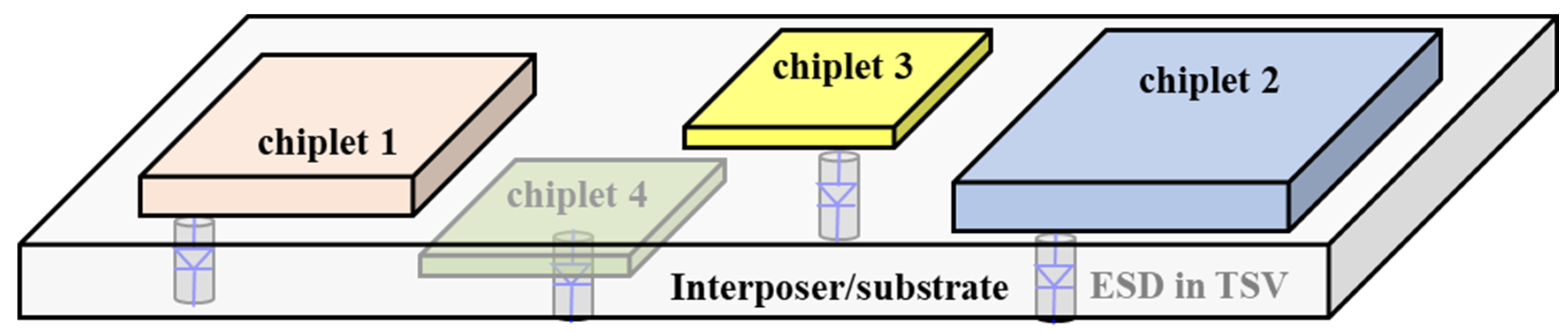
Upfront, the main goal of heterogeneous integration is to hetero-integrate different devices made in dissimilar materials using different process technologies into a 3D SoIC chipset, as depicted in Figure 3, to deliver rich functionalities and ultra performance. Consequently, the resulting vast functional and structural heterogeneity demands an entirely new ESD protection strategy, i.e., holistic ESD protection for SoICs, which is very different from on-chip ESD protection for monolithic chips. Practically, ESD charging and discharging involve the whole microsystem, being SoC or SoIC. Compared to a single-chip SoC, a heterogeneous SoIC is a much more complicated microsystem, where ESD charging and discharging are orders of magnitude more complex and sometimes may induce new ESD phenomena. SoICs typically involve many different materials having very different sensitivities to electrostatic charges, heat generation and thermal conduction. Furthermore, SoICs utilize many emerging bonding and packaging technologies, such as interposers and substrates (e.g., glasses), through-silicon vias (TSVs) and through-glass vias (TGVs), embedded Si bridges, micro bumps, copper pillars, Cu-Cu bonding, redistribution layers (RDL), 2D/2.5D/3D packaging, and chip-on-wafer-on-substrate (CoWoS) packaging, to name a few. Together, ESD phenomena become extremely complicated for SoICs. Hence, good on-chip ESD protection for a standalone chip and summation of ESD protection for all constituent chiplets cannot guarantee robust ESD protection for an SoIC microsystem. Therefore, an entirely new reliability design mindset is required, that is, a holistic ESD protection strategy, which treats the SoIC as a whole microsystem and considers ESD charging and discharging across the whole SoIC in a global view. Referring to Figure 1, a holistic ESD protection solution for SoIC requires a complete ESD protection network across the SoIC microsystem, where special attention must be given to overall ESD discharging routes, globally and locally, within the packaged SoIC. In principle, holistic ESD protection for a 3D HI SoIC chipset must be cross-layer, cross-domain and cross-chiplet within a microsystem, which requires ESD-technology co-development, ESD-IC co-design and ESD-SoIC co-simulation. In practical designs, holistic ESD protection for SoICs requires accurate design of ESD-critical parameters and compliance with ESD design windows at the SoIC level, which in turn requires new ESD design techniques to estimate SoIC-equivalent ESD-critical parameters, SoIC-equivalent ESD design windows, and SoIC-equivalent ESD discharging paths. It will also be very beneficial to explore non-traditional, truly disruptive ESD protection concepts to facilitate flexible SoIC construction using chiplets (i.e., multi-domains, multi-supplies, multi-technologies and multi-dies) coming from different vendors using different technologies. For example, field-programmable ESD protection designs may be very beneficial to constructing SoICs in the field to deal with any uncertainties associated with different chiplets from different vendors, e.g., handling process variations and replacing faulty chiplets for supply chain resilience [9].
Figure 3.
Illustration of a SoIC comprising multiple chiplets bonded on a substrate or interposer. Also shown is the interposer-based internal-distributed ESD protection network for SoIC, utilizing conceptual in-TSV ESD protection diodes.
2.2. Heterogeneity-Induced Interface and Interaction Complexity
Heterogeneity—the desired core feature of heterogeneous integration—will inevitably introduce complex interfaces and associated sophisticated interactions between dissimilar materials and heterogeneous structures, for example, die-to-die and chiplets–package interfaces, chiplet–package interactions (CPIs), and chiplet–package–board interactions (CPBIs). The inherent heterogeneity-induced interface and interaction complexity will substantially increase ESD vulnerability and ESD protection design difficulties for SoICs. Consequently, one major emerging in-SoIC ESD protection research objective is to thoroughly investigate the SoIC interfacing effects (e.g., thermal conduction boundaries and charge movement barriers) and the associated CPI/CPBIs, which will not only complicate ESD protection designs for SoICs, but also possibly induce new ESD phenomena. Research into such in-SoIC interfacing and interactive effects is extremely difficult due to many different factors involving materials, devices, processes, dies, packages, substrate carriers, boards, etc. For instance, the construction of SoICs requires using interposers, TSV/TGV, Si bridges, µ-bumps and RDL, which will significantly affect ESD charging, internal static charge distribution, ESD discharging routes, overheating and hot spots, ESD weak points, etc., which is substantially more complex than their SoC counterparts. Simply cloning on-chip ESD protection for monolithic chips to heterogeneous SoIC chipsets would surely be the recipe for ESD design failures.
2.3. ESD-SoIC Co-Design
It is well-known that ESD-IC co-design is important for on-chip ESD protection designs for advanced monolithic ICs, particularly for high-speed, high-frequency and high-data-rate chips, because any ESD protection structures will inevitably induce parasitic effects (e.g., CESD, noises and leakage) that can seriously affect IC performance [10,11,12,13,14,15]. For SoICs, significant research efforts must be devoted to developing new ESD-SoIC co-design methodologies to achieve holistic ESD protection for SoICs by adequately handling the complex in-SoIC interfacing effects and various interactions. Similar to SoC chips, ESD-SoIC co-design aims to achieve best ESD protection and highest SoIC performance simultaneously; however, the level of co-design difficulty will be ballooned due to the heterogeneity nature of SoICs. Uniqueness must be considered in ESD-SoIC co-design. For example, in the chip manufacturing phase, strict ESD control protocols are well in place in both fab and assembly lines; hence, it is viable for reducing die-level chiplet ESD protection while still being able to achieve robust ESD protection at SoIC level using a holistic ESD protection strategy. This is particularly important for advanced SoICs featuring extreme data rates (e.g., 5G/6G wireless communications, GPU and CPU for AI data centers and autonomous driving) where even tiny ESD-induced parasitic effects (e.g., CESD, noises and leakage) can seriously affect SoIC performance. Therefore, for SoICs, innovation in ESD protection is highly desirable in order to balance ESD robustness and SoIC specifications. For example, a field-dispensable ESD concept may be a viable solution to simultaneously deliver robust ESD protection and high SoIC performance (e.g., for AI data centers) [16].
2.4. New ESD Modeling and CAD Techniques
Significant research is expected on developing new ESD modeling and holistic ESD co-simulation techniques at the SoIC level to support SoIC ESD protection design optimization, prediction and verification. Accurate ESD modeling plays a key role in CAD-based ESD protection designs [17,18,19,20,21,22]. The vast heterogeneity of SoICs leads to new ESD modeling complexity that must be addressed for good ESD protection design flows. For example, new models have to be developed to tackle the complicated physical and thermal boundaries within SoICs, which will inevitably affect transient thermal boundary conditions, heat generation, thermal conduction flow, and hot spot formation. It is well-known that the heat dissipation flow critically depends upon the associated thermal boundary conditions. It is also recognized that fast ESD transients induce floating hot spots inside the IC, which creates transient, varying internal thermal boundaries associated with ESD-induced hot spots, making it very difficult to solve thermal conduction equations under ESD stressing. These effects are much more significant for SoICs due to the complex functional and structural interfaces, which will make ESD modeling for SoICs much more complicated.
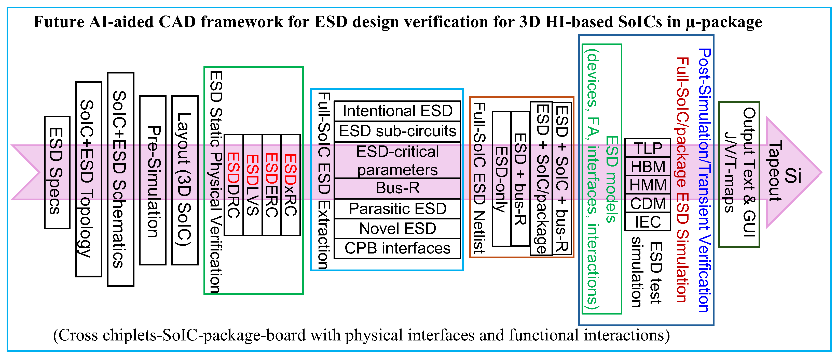
On the other hand, CAD-based ESD protection design methodologies play a vital role in on-chip ESD protection design optimization and prediction, as well as ESD physical design verification [6]. For SoICs, holistic ESD co-simulation becomes much more important, which requires developing new ESD CAD algorithms and software to conduct atom-to-system holistic simulation at the SoIC level that will involve both numerical and schematic simulation across the SoIC and the package. Smooth transition of simulation between chips, boards and packages is a huge challenge in the CAD field. Such CAD techniques and tools are currently almost entirely missing for SoIC ESD protection designs. It is important to note that CAD-based full-SoIC ESD design verification is highly desirable to ensure first-design success in making SoIC chipsets, hence minimizing SoIC development costs and shorten the time-to-market due to design iterations. Figure 4 highlights the desired features for future SoIC ESD CAD techniques. The key CAD features desired for SoIC-level ESD protection design include auto-extract ESD devices within SoIC, auto-extract SoIC-equivalent ESD-critical parameters, auto-extract SoIC-level ESD netlists, and auto-extract SoIC-level ESD discharging paths, all achieved by analyzing SoIC physical design data files (equivalent to GDSII layout data for monolithic chips). Next, the new ESD CAD needs to support conducting ESD-function-based ESD design verification at the SoIC chip level. ESD-function-based design verification must analyze in-SoIC ESD protection functions, including all SoIC-equivalent ESD-critical parameters (Vt1, It1, t1, Vh, Ih, RON, Vt2, It2, etc.), instead of simple ESD design rule checking (e.g., extra spacing for ESD protection structures). Furthermore, new ESD CAD should support in-SoIC ESD stressing test simulation, i.e., allowing the use of various ESD stimuli to zap an SoIC to reveal transient internal ESD discharging behaviors to examine possible ESD failures, which aims to dramatically reduce SoIC ESD development costs and time-to-market. Importantly, such new SoIC ESD CAD techniques must support holistic ESD-SoIC co-simulation involving interposers, substrates and packages, which substantially complicate the SoIC-induced interfacing effects and interactions. It is expected that artificial intelligence will play a key role in developing new ESD CAD methods for SoICs.
Figure 4.
Suggested new ESD CAD flow for holistic SoIC ESD protection design verification.
2.5. Non-Traditional ESD Protection Concepts
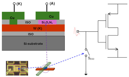
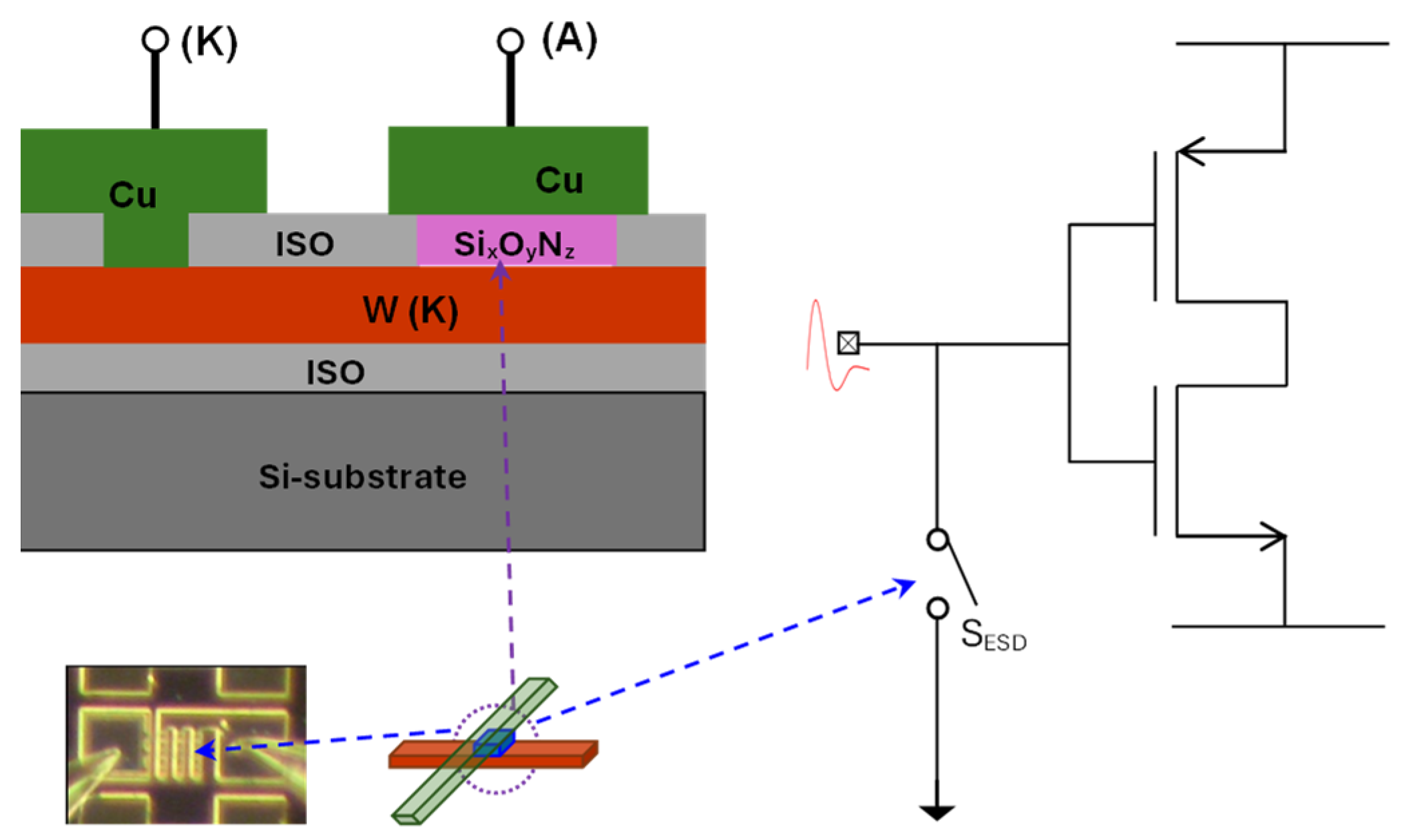
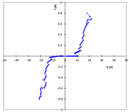
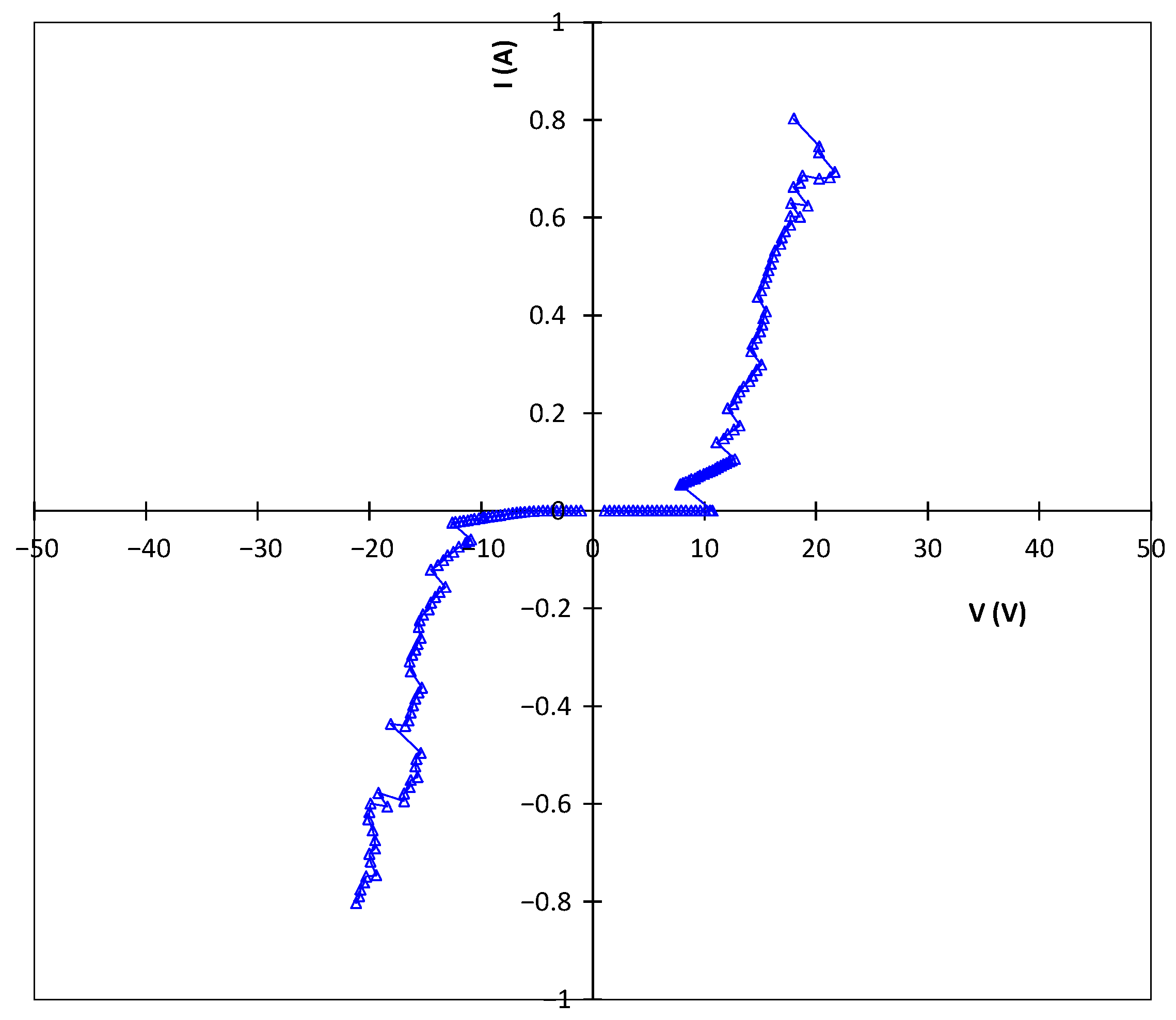
As discussed, the heterogeneity nature of SoICs makes ESD protection for SoICs very difficult if one sticks to the old mindset of ESD protection designs. For example, using full ESD protection network on a chip, shown in Figure 1, often requires that multiple PN-junction-based ESD protection devices be used for each pad of IC, which inherently leads to significant ESD-induced design overhead effects, including parasitic parameters (CESD, noises and leakage) that seriously affect IC specifications, while large ESD device sizes consume the Si asset and make full-chip layout floor planning very difficult. Therefore, research should be focused on exploring non-traditional, truly disruptive ESD protection concepts, which may potentially benefit SoIC ESD protection designs. It is noteworthy that ever since ESD failure was recognized as an IC reliability risk, for several decades, on-chip ESD protection has been following the golden rule that in-silicon PN-based ESD discharging devices are used for on-chip ESD protection, which unfortunately introduces substantial ESD-induced overhead effects inevitably. While ESD-IC co-design has been utilized to address the contradiction between IC performance and ESD protection, it may only be useful to a certain extent. On the other hand, any novel ESD protection concepts may potentially revolutionize ESD protection design practices. To this end, one is reminded that, fundamentally, on-chip ESD protection relies on using a well-controlled ESD discharging switch to realize ESD protection; theoretically, there might be many different ways to make good ESD discharging switches. For example, new phase-changing materials may be synthesized to make novel ESD discharging switch devices in the backend of the line (BEOL) in CMOS platform, as depicted in Figure 5 [23]. In this demonstration, a two-terminal above-IC nano crossbar ESD switch array was proposed, which comprises two metal electrodes (anode, A, and cathode, K) sandwiched between a phase-changing insulator. The nano crossbar ESD switch, connected to IC pads, stays turned off during normal IC operations and can be turned on by an incident ESD pulse to form a low-R ESD conduction path to protect the IC. A nano crossbar node device is required to ensure swift switching enabled by the phase-changing insulator. On the other hand, a large nano crossbar array can be designed to handle large ESD transient energy, hence providing high ESD protection. Figure 6 shows measured ESD discharging I-V characteristics under ESD stress by transmission-line pulse (TLP) testing [24], which demonstrates near-symmetric ESD discharging behavior. It is important to note that this nano crossbar ESD switch is made in the CMOS BEOL deck, i.e., above the Si substrate (above-IC), and it features dual-directional ESD discharging, which can dramatically reduce ESD-induced design overhead effects. This phase-changing ESD switch concept shows particular advantages to SoIC ESD protection because holistic in-SoIC ESD protection may utilize such phase-changing ESD switch devices both in individual chiplets and on interposers and in the package. For example, it is impossible to make any PN-based ESD protection structures in a glass interposer or substrate in SoICs. Obviously, when exploring novel non-traditional ESD protection concepts, thorough R&D efforts are needed, both to comprehensively evaluate any new ESD protection structures and to study practical implementation in real-world designs beyond initial feasibility prototyping. For example, regarding the ESD protection specifications of the new phase-change nano crossbar array ESD protection structure discussed, questions arise on how fast the phase-changing speed will be (mostly dominated by the phase-changing mechanisms, e.g., filament formation or the local tunneling effect) relevant to the targeted ESD transients (e.g., HBM ESD pulses of 2–10 ns speed or CDM ESD transients at 200–400 pS speed), what the ESD-induced CESD will be (e.g., exploring ultralow-k dielectrics as the phase-changing materials featuring ultrahigh ROff/ROn ratio), how stable will the new phase-change materials under ESD stresses be (including thermal stability), etc. From a CMOS implementation viewpoint, heterogeneous integration must be carefully investigated in order to hetero-integrate any novel ESD protection structures into mainstream CMOS technologies, for example, will the selected phase-changing materials be suitable for CMOS backend integration (including planarization, contamination and thermal budget in fabrication)? In summary, one should think non-traditionally when developing holistic ESD protection for 3D heterogeneous SoICs in µ-packages.
Figure 5.
Demonstration of a novel nano crossbar ESD switch array including its conceptional cross-section, fabricated die image and on-chip ESD protection scheme.
Figure 6.
TLP-measured ESD discharging I–V curve for a prototype nano crossbar ESD switch array shows desired symmetric ESD protection characteristics.
2.6. Leveraging Unique SoIC Features
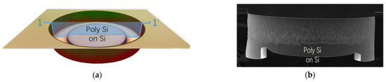
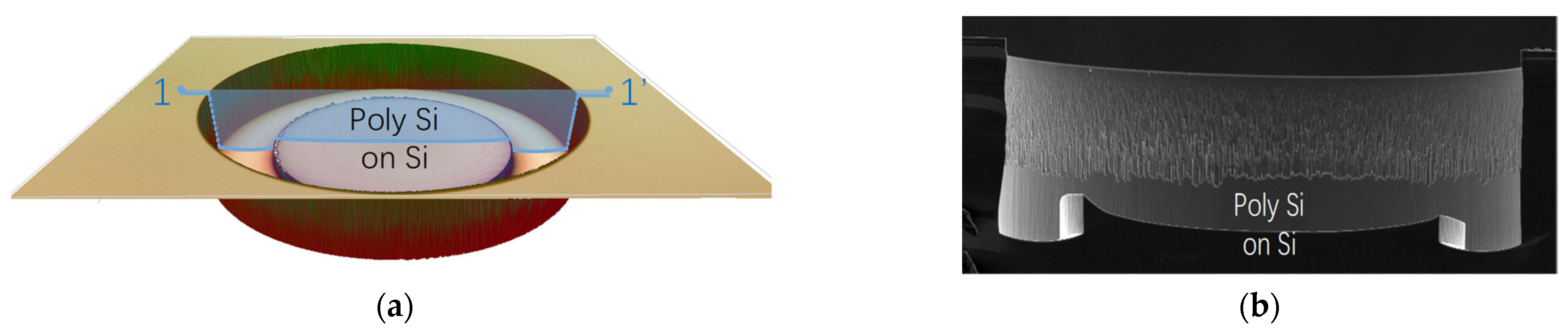
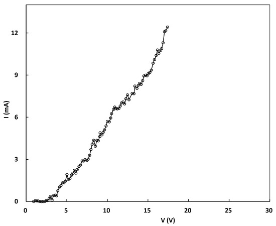
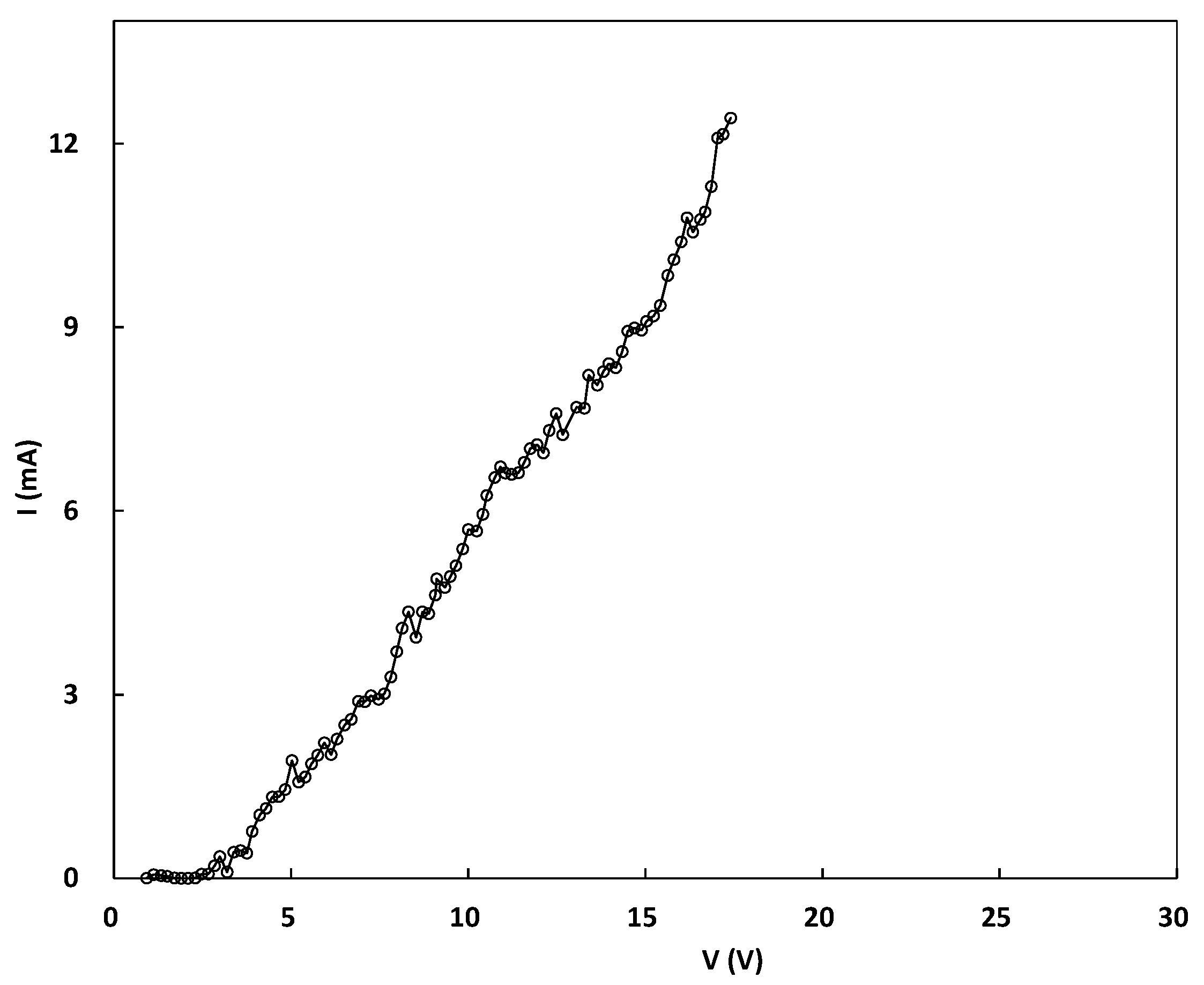
While the complexity of 3D heterogeneous SoICs generally makes ESD protection designs very challenging, one should also explore possibly utilizing some unique features for in-SoIC ESD protection. Non-traditional thinking again plays a key role in this regard. For example, since SoICs typically use special interposers and substrates, one novel solution will be to consider interposer-based ESD protection for SoICs in packages. Figure 3 illustrates placing ESD protection devices on an interposer in a distributed way that may have several benefits. Chiplet-level ESD protection may be minimized (just to ensure ESD protection in manufacturing) to realize the highest chiplet performance and to reduce ESD die area consumption, while full-SoIC ESD robustness will be achieved by using interposer-based ESD protection. In another example, TSV or TGV holes can be used to host vertical in-TSV ESD protection device in an interposer that has several benefits. A simple diode or resistor ESD protection device can be made inside TSV or TGV holes using backside engineering via HI technologies. The in-TSV ESD devices can be placed directly under bonding pads. The vertical in-TSV ESD devices can discharge large ESD transients in a vertical way directly to a local GND. Together, in-TSV/TGV ESD protection features a short, vertical and direct ESD discharging path, which means better thermal management, minimized local overheating, reduced risk of hot spots, and higher ESD protection. Figure 7 shows a vertical prototype in-TSV ESD diode made using a CMOS-compatible process flow and Figure 8 depicts the measured ESD discharging I–V curve by the TLP stressing test [25]. Indeed, it is worth thinking non-traditionally in exploring novel ESD protection structures that leverage unique features of SoICs.
Figure 7.
Images of a prototype in-TSV ESD diode by: (a) confocal microscope, and (b) SEM.
Figure 8.
TLP ESD stressing test shows expected ESD discharging I–V curve for a prototype in-TSV ESD diode.
2.7. New ESD Phenomenon
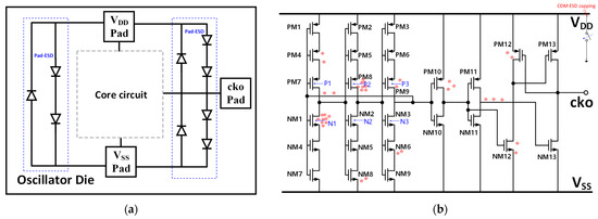
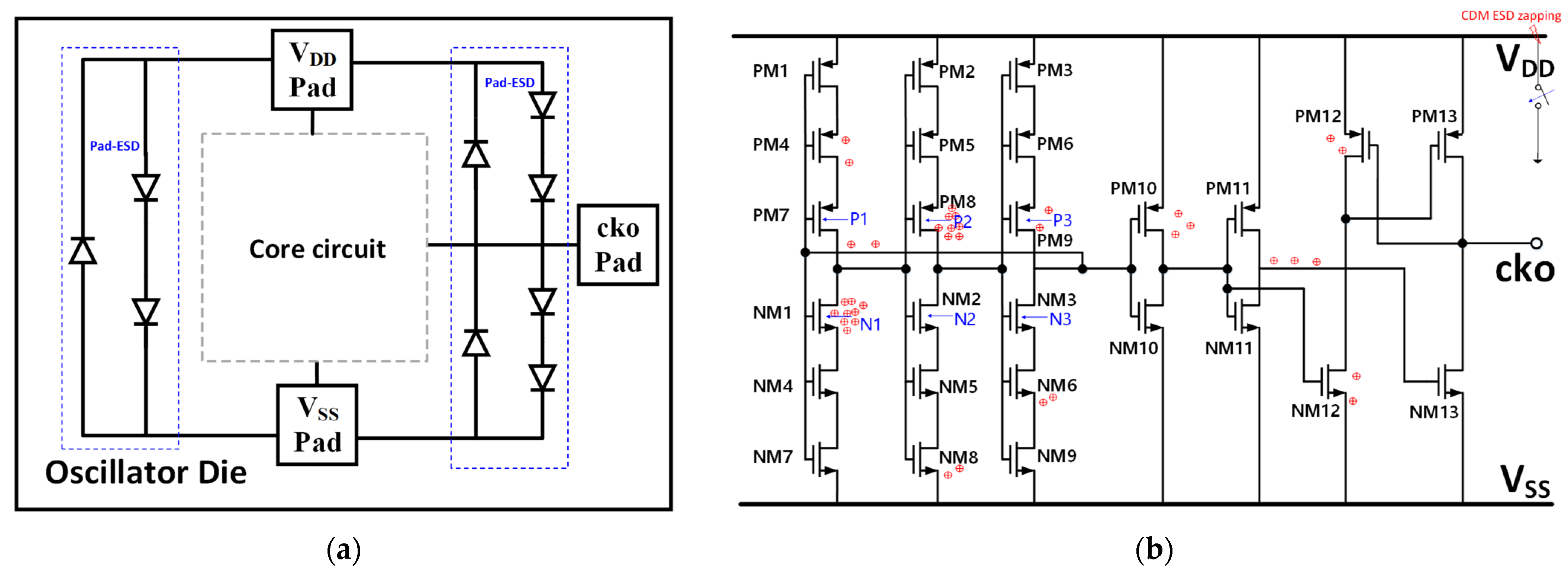
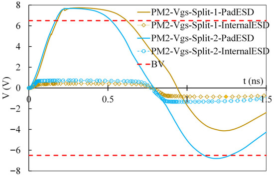
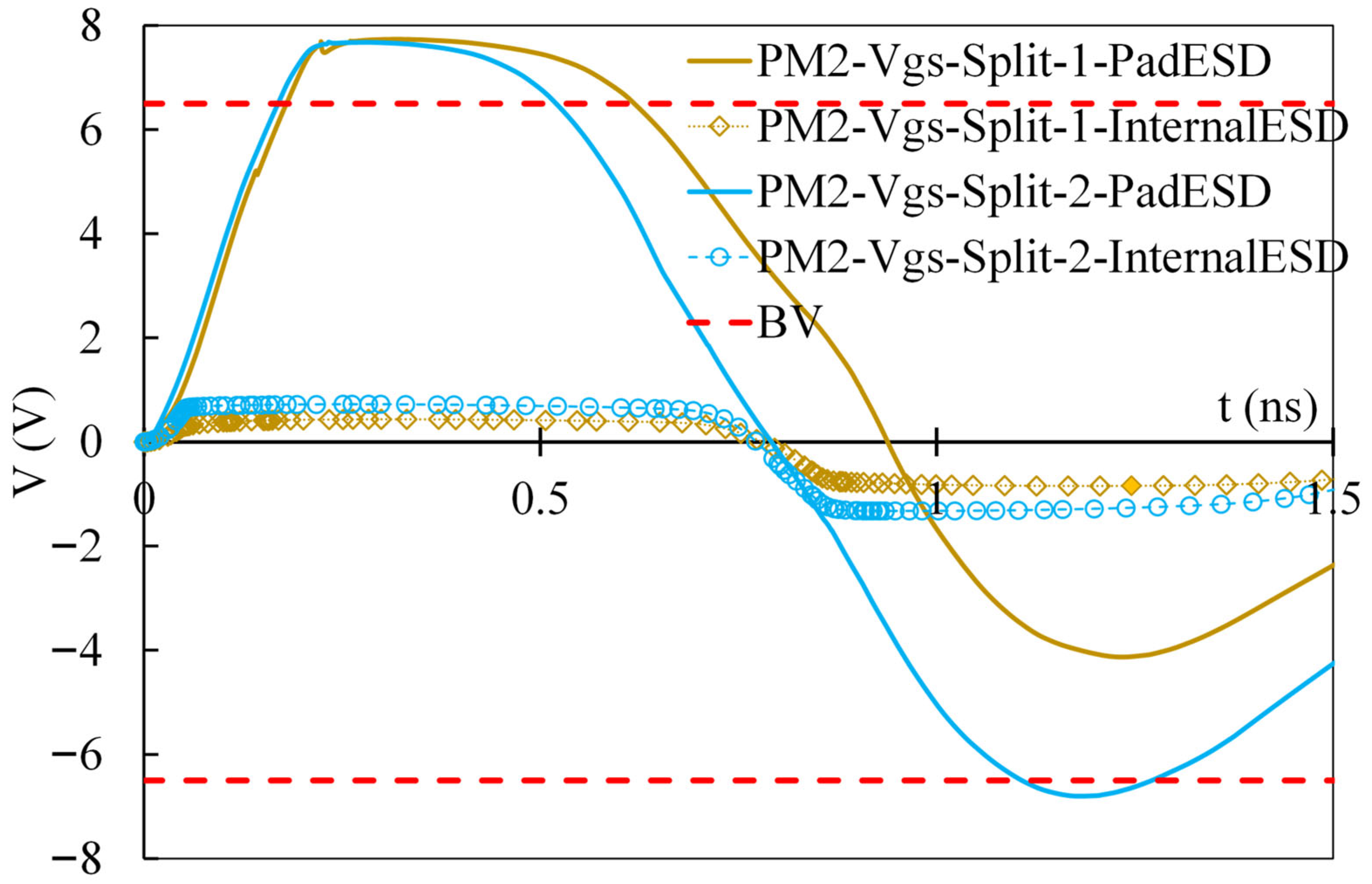
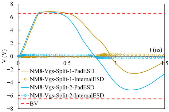
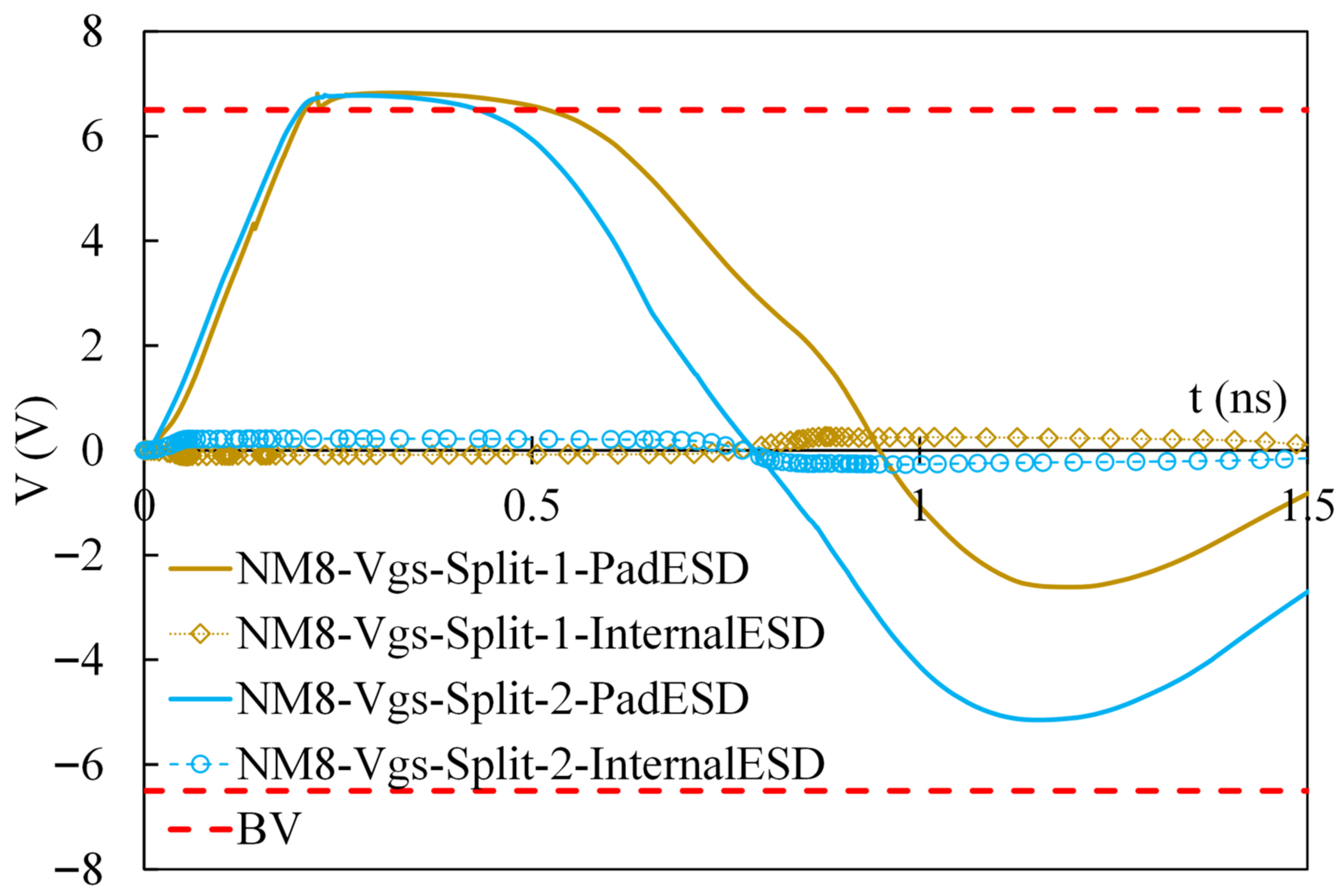
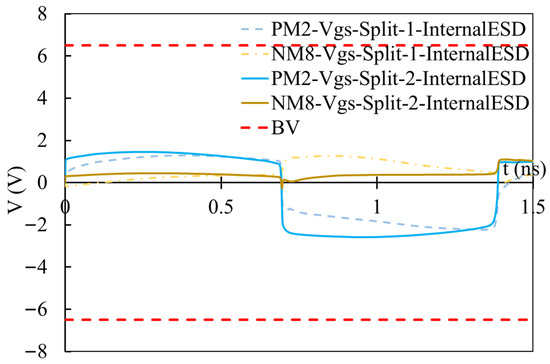
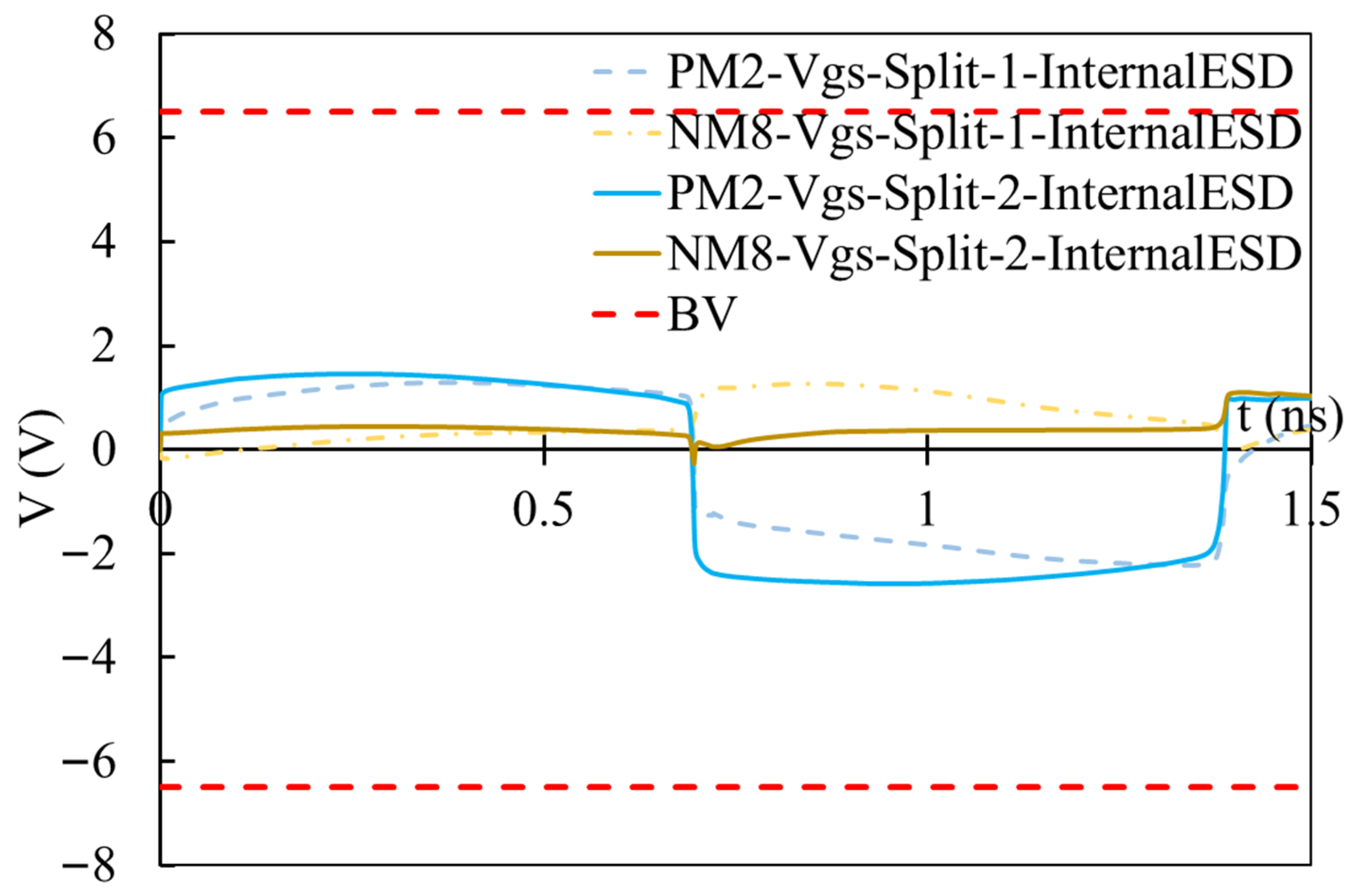
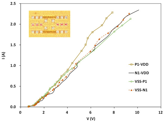
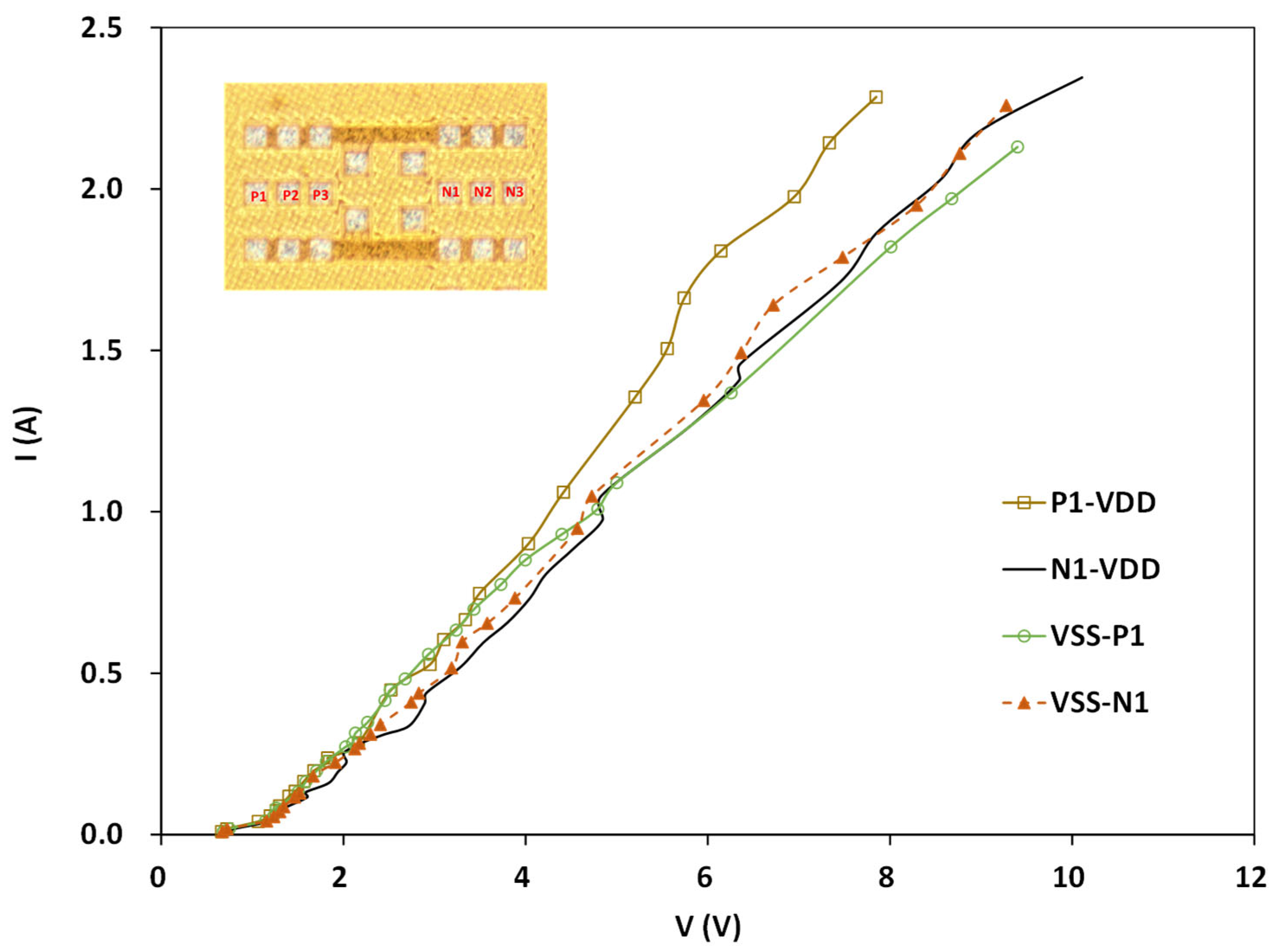
It is noteworthy that the heterogeneous complexity of 3D SoIC microsystems will likely introduce new ESD phenomena that can be different from the ESD events seen in monolithic SoC chips, which will in turn affect holistic ESD protection designs for SoICs. New ESD phenomena may substantially complicate the ESD reliability field, from the ESD failure mechanism to ESD protection design and ESD testing. For example, new ESD phenomena may blur the boundaries of existing industrial ESD test models including the human body model (HBM) and the charged device model (CDM) [26,27], etc., affecting ESD characterization and causing ESD protection uncertainty. Research is hence needed to investigate any possible new ESD phenomena and to develop suitable ESD protection for SoICs accordingly. One such case requiring urgent research is CDM-type ESD events for SoICs. Recently, it was reported that traditional pad-based CDM ESD protection for ICs may be fundamentally faulty [28]. Generally, most ESD test models, including HBM, MM, IEL and HMM [29,30,31], deal with from-external-to-internal ESD phenomena in nature. During these ESD events, external charges appear at bonding pads and try to enter IC dies through the pads. Classic pad-based on-chip ESD protection works in such a way that ESD protection devices are placed at the pads that can be turned on by incoming ESD transients, which will then discharge the incident ESD pulses into GND. Therefore, pad-based ESD protection utilizes at-pad ESD devices as a door keeper that blocks external charges from getting into a chip; hence, this offers ESD protection during any from-external-to-internal ESD events [5]. On the other hand, CDM ESD is entirely different in that static charges are induced into and stored inside a chip; when any one pad is grounded, the charges stored will be discharged into the ground via a transient GND. Obviously, CDM ESD is a from-internal-to-external phenomenon that is entirely different from a HBM ESD event that is a from-external-to-internal phenomenon. It is understandable that, while CDM ESD protection traditionally also uses the classic pad-based ESD protection method, it may not guarantee CDM ESD protection due to several reasons: internal charges may be stored anywhere and the charges may take any routes to discharge from inside the chip to GND. It is likely that internal damage may occur somewhere during CDM ESD even though the at-pad ESD devices may function perfectly. This may be the reason that CDM ESD failures are quite random in field. To address this unique CDM ESD problem, a non-pad-based internal distributed CDM ESD protection method was reported recently where, instead of using at-pad ESD devices, suitable ESD devices are placed inside an IC at certain key nodes. The idea is that, as charges accumulate internally to a certain level, the internal ESD device will be turned on to discharge these charges locally and internally, without having to route internally to reach to the grounded pad for at-pad ESD discharging [32]. The following example explains the new non-pad-based internal-distributed CDM ESD protection method concept [32]. Figure 9 depicts a three-stage oscillator circuit designed in a 45 nm SOI CMOS where some MOSFETS (NM1, NM2, NM3, PM7, PM8, PM9) are purposely designed “large”, hence being able to hold more static charges randomly induced into the IC, modeling the CDM ESD internal charge storage situation. Two ESD protection cases are studied: Figure 9a shows a design split using classic pad-based ESD protection, while Figure 9b is a design split using non-pad-based internal-distributed ESD protection for the same oscillator circuit. Figure 9b depicts a general CDM ESD case where charges may be induced into and stored inside the IC in a random way; in the example shown, more charges accumulate around large MOSFETs (e.g., NM1 and PM8), which will be discharged during the CDM ESD protection period. Two internal-oriented CDM ESD discharging splits are simulated, assuming the charges are from around the NM1 source (Split 1) and the PM8 source (Split 2). The circuit-level CDM ESD simulation was first conducted for 50 V CDM ESD discharging when the VDD pad is grounded, following the industrial CDM ESD test model. The ESD failure criterion used is the breakdown voltage for MOSFETs, which features BVOX ~6.5 V for the 45 nm SOI technology. Figure 10 and Figure 11 show transient VGS for PM2 and NM8 induced by 50 V CDM ESD discharging, respectively. It is observed that when using classic pad-based ESD protection, gate voltage breakdown will occur for both Split 1 and Split 2 discharging cases, resulting in internal CDM ESD failure to PM2 and NM8 (as an example). On the contrary; however, when using internal-distributed CDM ESD protection devices placed at concerned large MOSFETs (NM1, NM2, NM3, PM7, PM8, and PM9, where more charges stored), very low CDM-induced transient voltage surges are observed for both Split 1 and Split 2 discharging cases, hence providing CDM ESD protection. Figure 12 shows that when using internal-distributed ESD protection, the circuit passes 500 V CDM ESD stressing without any internal ESD failure for both internal CDM ESD discharging cases (Split 1 and Split 2). In the fabricated ICs, the internal CDM ESD protection diodes were stressed by very-fast TLP (VFTLP) test for CDM ESD characterization [33], which shows expected CDM ESD discharging I-V curves, depicted in Figure 13.
Figure 9.
Simplified schematic for a s-stage oscillator IC using (a) class pad-based CDM ESD protection and (b) new non-pad-based internal distributed CDM ESD protection. The circuit in (b) is the same as the core circuit in (a). CDM charge storage in (b) is exemplar where assuming major CDM ESD comes from large volume of charges accumulated around large NM1 and PM9. CDM ESD stress test is conducted by grounding the VDD pad.
Figure 10.
CDM ESD circuit simulation under 50 V CDM ESD stress shows transient internal voltage surges to exemplar PM2 of the oscillator IC, suggesting CDM ESD breakdown occurs when using pad-based CDM ESD protection. However, no ESD failure is observed when using non-pad-based internal-distributed CDM ESD protection. Note: two exemplar internal CDM ESD discharging cases are studied: Split 1 for charges coming from around NM1 as the CDM source and Split 2 for PM8 as the CDM discharging source.
Figure 11.
CDM ESD circuit simulation under 50 V CDM ESD stress shows transient internal voltage surges to exemplar PM8 of the oscillator IC, suggesting CDM ESD breakdown occurs when using pad-based CDM ESD protection. However, no ESD failure is observed when using non-pad-based internal-distributed CDM ESD protection. Note: two exemplar internal CDM ESD discharging cases are studied: Split 1 for charges coming from around NM1 as the CDM source and Split 2 for PM8 as the CDM discharging source.
Figure 12.
CDM ESD circuit simulation under 500 V CDM ESD stress shows transient internal voltage surges to exemplar PM2 and NM8, suggesting the oscillator IC can pass 500 CDM ESD stress when using non-pad-based internal-distributed CDM ESD protection for both Split 1 and Split 2 CDM ESD discharging sources.
Figure 13.
Measured CDM ESD discharging I-V curves by VFTLP test for fabricated internal-distributed CDM ESD diodes shows the expected CDM ESD discharging behaviors. Inset is a die photo for the oscillator IC where internal-distributed CDM ESD protection diodes are placed at selected internal nodes (P1, P2, P3, N1, N2, N3) near the large MOSFETs.
Carrying on from the above example of using non-pad-based internal-distributed CDM ESD protection for monolithic ICs, we believe that the actual CDM ESD phenomena for SoICs can be much more complicated compared to that for SoC chips, due to heterogeneity. First, the heterogeneous complexity will significantly complicate CDM charge induction procedures, as well as internal charge storage and distribution associated with the complex structural and materials interfaces. Second, the complex SoIC structure will make internal CDM ESD discharging routing under CDM ESD stressing much more complicated and unpredictable. Third, the complex heterogeneity may create many unexpected ESD weak points inside the SoIC, making it more vulnerable to internal CDM ESD failures. Even worse, internal CDM ESD failures will surely be more random. It is noteworthy that significant research efforts should be given to understanding the SoIC microsystem as a whole aiming to evaluate impacts of SoIC complexity on new ESD phenomena. For example, charge induction into SoIC will be highly sensitive to the materials properties of the different materials used in different chiplets and packages; internal CDM-like ESD routing will be mostly relevant to 3D chiplet bonding, stacking and packaging structures and methods, etc. Furthermore, such materials and structural heterogeneities will play a key role in smart partitioning a SoIC microsystem for developing optimal intelligent internal-distributed CDM/HBM ESD protection strategy. Reasonably, CDM ESD phenomena in SoICs may have a hybrid nature: when considering internal charges to stress a specific single chiplet, it is a from-external-to-internal ESD event (similar to HBM) to that die; however, from the whole SoIC viewpoint, it is a from-internal-to-external ESD event (similar to CDM ESD for monolithic chips). Therefore, a hybrid HBM/CDM ESD model may be developed to address the complex CDM-type ESD phenomena for SoICs, which requires thorough research.
Another new ESD phenomenon for SoICs is backside ESD stressing where ESD discharging may occur when incident ESD transients occur to the backside of a chiplet, i.e., when handling a die during 3D stacking [34,35]. Unlike traditional pad-/pin-occurring ESD events, backside ESD zapping may not be modeled by existing pad-based ESD test models, such as HBM.
2.8. AI for ESD
Artificial intelligence (AI) can be leveraged to investigate complex ESD phenomena and to develop novel ESD protection solutions, particularly for 3D heterogeneous SoICs in advanced packages, which will be a major new research topic in the ESD reliability field. It is recognized that ESD reliability is very knowledge-centric, data-driven, and full of magics and unknowns, hence leading to a common statement that ESD protection design is art and experience dominant. This is where AI can play a critical role. Obviously, it will be very beneficial to combine expert brains together globally and to develop ESD-specific AI algorithms and methods for investigating ESD phenomena and developing ESD protection solutions. For example, ESD modeling and data analysis depend on seas of data and statistical data analysis plays a key role. It is hence very beneficial to use AI algorithms for self-learning from and self-training with large ESD databases and successful ESD protection design experiences, and to use machine learning (ML) methods to analyze big ESD data to guide ESD protection designs. Recently, ML has been used to develop ESD models and assist ESD designs [36,37,38,39]. Additionally, AI can be used to handle otherwise impossible ESD protection design tasks. For example, AI may be used to analyze transient ESD-induced hot spots inside ICs with complex materials boundaries. AI can also be used to study internal charge storage and distribution for chips under CDM ESD stressing, hence revealing internal CDM ESD discharging routing and identifying internal ESD weak points in complex chips. For complex SoICs, AL can be used to smart partitioning a full SoIC microsystem to intelligently identify where and how CDM-induced charges are distributed inside the SoIC, hence guiding the smart placement of internal-distributed CDM ESD protection devices inside the SoIC for CDM ESD protection. ESD-specific large language models (LLMs) can be developed that will be very beneficial for practical ESD protection designs to address data complexity and uncertainties. Considering the heterogeneous complexity of SoICs in advanced packages, AI will be a much more useful and powerful tool for holistic ESD protection for SoICs. It is expected that a global ESD reliability ecosystem, e.g., AI-for-ESD Forum, may be built up to serve the purpose of SoIC ESD reliability research. Particularly, combining the bottom-up approach (physics-based) and the top-down approach (data-driven), future AI-for-ESD techniques will revolutionize the SoIC ESD protection design field. Similar on-going research on open-source design methodologies has been reported [40] recently.
2.9. New ESD Test and Compliance Standards
Good ESD protection design must be evaluated by ESD testing, which follows various industrial ESD test models and standards. It is expected that SoIC ESD protection will need some new ESD test standards and ESD compliance standards. For ESD testing, continuous R&D efforts have been given to validate existing ESD test models for new chips and as needed, to develop new ESD test models for new ESD phenomena. For example, the human metal model (HMM) was recently developed to address the hybrid nature of component level and system level ESD stressing by modeling a human being holding a metal object, e.g., when connecting a GPU chip with an optical cable. In another example, CDM ESD test uncertainty, a big headache to IC designers, may be associated with the not-so-good existing CDM ESD test model, i.e., field-induction CDM (FICDM), which should be re-evaluated for its usefulness. For SoIC ESD protection designs, one research objective will be to thoroughly understand the CDM-type ESD phenomenon and develop adequate new CDM ESD test method that can model the hybrid HBM/CDM nature for SoICs as discussed before. On the other hand, an SoIC with or without package is a microsystem comprising many chiplets; hence, new microsystem-level ESD test methods are needed, for example, similar to the IEC ESD test standard developed for system-level ESD stressing. However, directly applying the IEC test method to SoICs may not be suitable since IEC was developed to stress large systems, not for chip-scale microsystems. Specifically, the ESD zapping points for SoICs will be more than the traditional pad/pin-stressing method, for example, backside ESD stressing should be considered for SoICs during 3D stacking.
Equally importantly is to explore new ESD Qualification and Compliance standards for ESD protection designs for SoICs. One key uniqueness for SoICs is that the constituent chiplets may come from different vendors, sometimes may change the fabrication technologies or switch between different packaging methods. Therefore, new industry ESD qualification and compliance standards for SoICs are highly desired in production, where chiplet-ESD interoperability is critical for supporting smooth operations and the resilience of global supply chains. SoIC ESD compliance is very important for the industry to reduce development costs and shorten time-to-market in developing new systems using heterogeneous SoICs, for example, when building up AI data centers. It is worth noting that any new ESD Qualification standards must treat the SoIC as a microsystem and address the microsystem-level specifications, instead of simply individual chiplets.
3. Summary
The core feature of 3D heterogeneous SoICs in advanced packages—the heterogeneity—makes ESD protection for SoICs a grand emerging reliability challenge. Critically, an entirely new strategic mindsets are required in handling ESD reliability problems for SoIC chips. Particularly, one must recognize that ESD reliability is a problem throughout the entire lifetime of any products and ESD risk is an everyday concern primarily related to end-users. While adequate ESD control in the making phase (e.g., manufacturing and assembly) is important and mature, supporting some reduction in ESD protection level at advanced technology nodes to accommodate ultrahigh IC performance [41,42,43], the real-world ESD risks never decrease in the end-users’ hands throughout the entire product life cycle. In fact, ESD reliability is a much bigger problem for SoICs and therefore requires more robust ESD protection, because devices made in advanced technologies (e.g., 2 nm node) are much more vulnerable to even lower ESD stresses, when in end users’ hands, while the costs of ESD failure of advanced SoIC chips are becoming unbearable. This article discusses future ESD research directions for 3D heterogeneous SoICs, where the key takeaway is that good ESD protection at SoIC level should go holistic by taking the entire SoIC microsystem as a whole into design consideration. These future SoIC ESD research objectives will be incorporated into the IEEE Heterogeneous Integration Roadmap (HIR), 2025 Edition.
Author Contributions
Conceptualization, A.W.; writing, X.L., R.M., Z.Y. and A.W. All authors have read and agreed to the published version of the manuscript.
Funding
This research received no external funding.
Data Availability Statement
Data are contained within the article.
Conflicts of Interest
The authors declare no conflicts of interest.
Abbreviations
The following abbreviations are used in this manuscript:
| ESD | Electrostatic discharge |
| SoIC | System-on-integrated-chiplets |
| HI | Heterogeneous integration |
| HBM | Human body model |
| CDM | Charged device model |
| TLP | Transmission line pulse |
| VFTLP | Very fast transmission line pulse |
| GND | Ground |
| RF | Radio frequency |
| AMS | Analog and mixed-signal |
| CAD | Computer-aided design |
References
- HIR: Heterogeneous Integration Roadmap, IEEE Electronics Packaging Society. Available online: https://eps.ieee.org/technology/heterogeneous-integration-roadmap/2024-edition/ (accessed on 18 February 2026).
- Amerasekera, E.A.; Duvvury, C. ESD in Silicon Integrated Circuits; Wiley: New York, NY, USA, 2002; ISBN 978-0471498711. [Google Scholar]
- Voldman, S. ESD: RF Technology and Circuits; Wiley: New York, NY, USA, 2006; ISBN 978-0470847558. [Google Scholar]
- Duvvury, C.; Gossner, H.; Shrivastava, M. High Current ESD: Physics and Design; Cambridge University Press: Cambridge, UK, 2026; ISBN 978-1107089051. [Google Scholar]
- Wang, A. Practical ESD Protection Design; Wiley-IEEE Press: New York, NY, USA, 2022; ISBN 978-1119850403. [Google Scholar]
- Pan, Z.; Li, X.; Hao, W.; Miao, R.; Wang, A. On-Chip ESD Protection Design Methodologies by CAD Simulation. ACM Trans. Des. Autom. Electron. Syst. 2023, 29, 1–41. [Google Scholar] [CrossRef] [Scilit]
- Li, X.; Pan, Z.; Hao, W.; Miao, R.; Yue, Z.; Wang, A. On-Chip ESD Protection: Device Innovation. IEEE Electron Devices Rev. 2024, 1, 1–15. [Google Scholar] [CrossRef] [Scilit]
- Hao, W.; Pan, Z.; Li, X.; Miao, R.; Yue, Z.; Wang, A. On-Chip ESD Protection: Design Innovation. IEEE Electron Devices Rev. 2024, 2, 32–51. [Google Scholar] [CrossRef] [Scilit]
- Shi, Z.; Wang, X.; Liu, J.; Lin, L.; Zhao, H.; Fang, Q.; Wang, L.; Zhang, C.; Fan, S.; Tang, H.; et al. Programmable on-Chip ESD Protection Using Nano Crystal Dots Mechanism and Structures. IEEE Trans. Nanotechnol. 2012, 11, 884–889. [Google Scholar]
- Liu, J.; Carels, N.; Peachey, N. Characterization and Analysis of RF Switches in SOI Technology for ESD Protection. In 2022 IEEE International Reliability Physics Symposium (IRPS); IEEE: New York, NY, USA, 2022. [Google Scholar]
- Huang, X.; Gan, X.; Li, B.; Liu, F.; Qian, L.; Wang, G. Overview of Co-design Considerations for ESD Protection in System-in-Packages (SiPs). In 2019 IEEE International Conference on Electron Devices and Solid-State Circuits (EDSSC); IEEE: New York, NY, USA, 2019. [Google Scholar]
- Lu, F.; Dong, Z.; Wang, L.; Ma, R.; Zhang, C.; Zhao, H.; Wang, A. A Systematic Study of ESD Protection Co-Design with High-Speed and High-Frequency ICs in 28 nm CMOS. IEEE Trans. Circuits Syst. I Regul. Pap. 2016, 63, 1746–1757. [Google Scholar] [CrossRef] [Scilit]
- Hao, W.; Pan, Z.; Li, X.; Miao, R.; Yue, Z.; Wang, A. ESD Co-Design of 38-GHz Traveling-Wave SPDT Switch in 45-nm PDSOI. IEEE Microw. Wirel. Technol. Lett. 2025, 35, 1756–1759. [Google Scholar] [CrossRef] [Scilit]
- Hao, Y.; Zhang, Q.; Bai, X.; Shi, Z.; Ma, H.; Cheng, Y. Co-design of ESD protection and LNA in RFIC. In 2013 IEEE International Conference on ASIC; IEEE: New York, NY, USA, 2013. [Google Scholar]
- Wang, A.; Feng, H.; Zhan, R.; Xie, H.; Chen, G.; Wu, Q.; Guan, X.; Wang, Z.; Zhang, C. A Review on RF ESD Protection Design. IEEE Trans. Electron Devices 2005, 52, 1304–1311. [Google Scholar] [CrossRef] [Scilit]
- Zhang, C.; Dong, Z.; Lu, F.; Ma, R.; Wang, L.; Zhao, H.; Wang, X.; Wang, X.S.; Tang, H.; Wang, A. Fuse-Based Field-Dispensable ESD Protection for Ultra-High-Speed ICs. IEEE Electron Device Lett. 2014, 35, 381–383. [Google Scholar] [CrossRef] [Scilit]
- Ammer, M.; Rupp, A.; Glaser, U.; Cao, Y.; Sauter, M.; Maurer, L. Application Example of a Novel Methodology to Generate IC Models for System ESD and Electrical Stress Simulation out of the Design Data. In 2019 IEEE Annual EOS/ESD Symposium (EOS/ESD); IEEE: New York, NY, USA, 2019. [Google Scholar]
- Yan, X.; Mousavi, S.; Shen, L.; Xu, Y.; Zhang, W.; Bub, S.; Holland, S.; Pommeremke, D.; Beetner, D. A Combined Model for Transient and Self-Heating of Snapback Type ESD Protection Devices. In 2023 IEEE Annual EOS/ESD Symposium (EOS/ESD); IEEE: New York, NY, USA, 2023. [Google Scholar]
- Zhang, F.; Wang, C.; Lu, F.; Chen, Q.; Li, C.; Wang, X.S.; Li, D.; Wang, A. A Full-Chip ESD Protection Circuit Simulation and Fast Dynamic Checking Method Using SPICE and ESD Behavior Models. IEEE Trans. Comput.-Aided Des. Integr. Circuits Syst. 2019, 38, 489–498. [Google Scholar] [CrossRef] [Scilit]
- Sakaguchi, N.; Koike, H.; Izukawa, M.; Hamada, T. Total Tester/PKG/Chip circuit-modeling methodology for predicting highly precise CDM breakdown voltage. In 2022 IEEE Annual EOS/ESD Symposium (EOS/ESD); IEEE: New York, NY, USA, 2022. [Google Scholar]
- Liang, H.-J.; Liu, J.-L.; Liang, H.-L. A novel high-precision compact SCR model for ESD protection circuit simulation using SPICE. In 2023 IEEE International Symposium on Next-Generation Electronics (ISNE); IEEE: New York, NY, USA, 2023. [Google Scholar]
- Zhang, K.; Wang, Y.; Jin, X. A Novel Modeling Method for BV Characteristics of ESD Protection Devices. In 2024 IEEE International Conference on Solid-State & Integrated Circuit Technology (ICSICT); IEEE: New York, NY, USA, 2024. [Google Scholar]
- Wang, L.; Wang, X.; Shi, Z.; Ma, R.; Liu, J.; Dong, Z.; Zhang, C.; Lin, L.; Zhao, H.; Zhang, L.; et al. Dual-Directional Nano Crossbar Array ESD Protection Structures. IEEE Electron Device Lett. 2013, 34, 111–113. [Google Scholar] [CrossRef] [Scilit]
- ANSI/ESD STM 5.5.1-2016; ESD Association Standard Test Method for Electrostatic Discharge (ESD) Sensitivity Testing—Transmission Line Pulse (TLP)—Component Level. The ESD Association: New York, NY, USA, 2016.
- Li, C.; Di, M.; Pan, Z.; Wu, H.; Wang, A. Vertical TSV-Like Diode ESD Protection. In Proceedings of the IEEE Electron Devices Technology and Manufacturing Conference (EDTM), Chengdu, China, 8–11 April 2021; pp. 1–3. [Google Scholar]
- ANSI/ESDA/JEDEC JS-001-2017; For Electrostatic Discharge Sensitivity Testing—Human Body Model (HBM)—Component Level. The ESD Association: New York, NY, USA; JEDEC: Arlington, VA, USA, 2017.
- ANSI/ESDA/JEDEC JS-002-2018; For Electrostatic Discharge Sensitivity Testing—Charged Device Model (CDM)—Device Level. The ESD Association: New York, NY, USA; JEDEC: Arlington, VA, USA, 2018.
- Di, M.; Li, C.; Pan, Z.; Wang, A. Pad-Based CDM ESD Protection Methods Are Faulty. IEEE J. Electron Devices Soc. (J-EDS) 2020, 8, 1297–1304. [Google Scholar] [CrossRef] [Scilit]
- ESD STM5.2-2012; Electrostatic Discharge Sensitivity Testing: Machine Model—Component Level. The ESD Association: New York, NY, USA, 2012.
- ESD SP5.6-2019; ESD Association Standard Practice for Electrostatic Discharge Sensitivity Testing—Human Metal Model (HMM) Component Level. The ESD Association: New York, NY, USA, 2019.
- IEC 61000-4-2; Electromagnetic Compatibility, Part 4: Testing and Measurement Techniques, Section 2: Electrostatic Dis-charge Immunity Test. The International Electrotechnical Commission (IEC): Geneva, Switzerland, 2008.
- Di, M.; Li, C.; Pan, Z.; Wang, A. Non-Pad-Based in Situ in-Operando CDM ESD Protection Using Internally Distributed Network. IEEE J. Electron Devices Soc. 2021, 9, 1248–1256. [Google Scholar] [CrossRef] [Scilit]
- ESD TR5.5-03-14; ESD Association Technical Report for Electrostatic Discharge (ESD) Sensitivity Testing–Very Fast–Transmission Line Pulse (TLP). Electrostatic Discharge Association: New York, NY, USA, 2014.
- Wadatsumi, T.; Kawai, K.; Hasegawa, R.; Miki, T.; Nagata, M.; Muramatsu, K. Voltage Surges by Backside ESD Impacts on IC Chip in Flip Chip Packaging. In Proceedings of the IEEE International Reliability Physics Symposium (IRPS), Dallas, TX, USA, 27–31 March 2022; pp. P14-1–P14-6. [Google Scholar]
- Wadatsumi, T.; Kawai, K.; Hasegawa, R.; Monta, K.; Miki, T.; Nagata, M. Characterization of Backside ESD Impacts on Integrated Circuits. In Proceedings of the IEEE International Reliability Physics Symposium (IRPS), Monterey, CA, USA, 26–30 March 2023; pp. 1–6. [Google Scholar]
- Liang, W.; Yang, X.; Miao, M.; Loiseau, A.; Mitra, S.; Gauthier, R. Novel ESD compact modeling methodology using machine learning techniques for snapback and non-snapback ESD devices. IEEE Trans. Device Mater. Reliab. 2021, 21, 455–464. [Google Scholar] [CrossRef] [Scilit]
- Moon, B.H.; O’Sullivan, G.; Andres, B.; Sharma, S.; Chen, H.; Chang, K.H. Advanced ESD Event Detection System Using Machine Learning Method. In 2025 47th Annual EOS/ESD Symposium (EOS/ESD); IEEE: New York, NY, USA, 2025. [Google Scholar]
- Nishad, S.; Kundu, S.; Richaud, N.; Mallikarjun, S.; Prasad, M.; Renker, L. MLESD: Machine Learning Assisted Faster On-Chip ESD Convergence Strategy. In 2024 IEEE International Conference on VLSI Design; IEEE: New York, NY, USA, 2024; pp. 281–286. [Google Scholar]
- Middaugh, C.; Nourani, M.; Duvvury, C.; Schichl, J. ESD Stress Data Analysis with Machine Learning: A Case Study. In 2023 Annual EOS/ESD Symposium (EOS/ESD); IEEE: New York, NY, USA, 2023. [Google Scholar]
- Industry Council on ESD Target Levels. White Paper 1: A Case for Lowering Component Level HBM ESD Specifications and Requirements, Industry Council on ESD Target Levels, 4th ed.; Industry Council on ESD Target Levels: Online, 2018. [Google Scholar]
- Goudroumanis, G.; Pantazi-Kypraiou, M.; Floros, G.; Tziouvaras, A.; Stamoulis, G.; Garc, A. 3DPX—An Open-Source Methodology for 3D Physical Design Exploration. arXiv 2025. [Google Scholar] [CrossRef] [Scilit]
- Industry Council on ESD Target Levels. White Paper 2: A Case for Lowering Component-Level CDM ESD Specifications and Requirements, Industry Council on ESD Target Levels, 3rd ed.; Industry Council on ESD Target Levels: Online, 2021. [Google Scholar]
- Smallwood, J. The ESD Control Program Handbook; Wiley-IEEE Press: New York, NY, USA, 2020; ISBN 978-1118311035. [Google Scholar]
Disclaimer/Publisher’s Note: The statements, opinions and data contained in all publications are solely those of the individual author(s) and contributor(s) and not of MDPI and/or the editor(s). MDPI and/or the editor(s) disclaim responsibility for any injury to people or property resulting from any ideas, methods, instructions or products referred to in the content. |
© 2026 by the authors. Licensee MDPI, Basel, Switzerland. This article is an open access article distributed under the terms and conditions of the Creative Commons Attribution (CC BY) license.