


Abstract
Optical through silicon vias (OTSVs) have been regarded as a promising alternative to conventional (electrical) through silicon vias (TSVs) for the next-generation electro-optic heterogeneous integration. This study systematically examines the influence of fabrication imperfections on the transmission performance in terms of incident light misalignment, via geometry variation, and sidewall roughness. The results demonstrate that over a finite range of beam widths, the insertion loss can be maintained at a relatively low level of less than −0.16 dBm, and this low-loss window broadens with increasing via diameter. Moreover, an increased diameter exhibits greater tolerance to the lateral offset, as for 10 μm, 20 μm, and 30 μm vias, the insertion loss rises to 3 dB at axis misalignments of 5 μm, 10 μm, and 15 μm, respectively. Additionally, smaller-diameter OTSVs are considerably more sensitive to sidewall slope angles than their larger-diameter counterparts. Additionally, minimizing the sidewall roughness is critical for maximizing the coupling efficiency, which suggests that the etch-passivation shift needs to be as quick as possible during the deep reactive ion etch (DRIE) process. With the proposed fabrication approach and comprehensive analysis of fabrication imperfection factors, this study provides essential insights for the development of high-performance OTSVs in advanced 3D optoelectronic integration.
1. Introduction
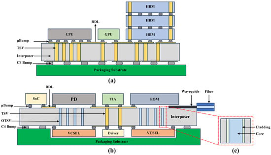
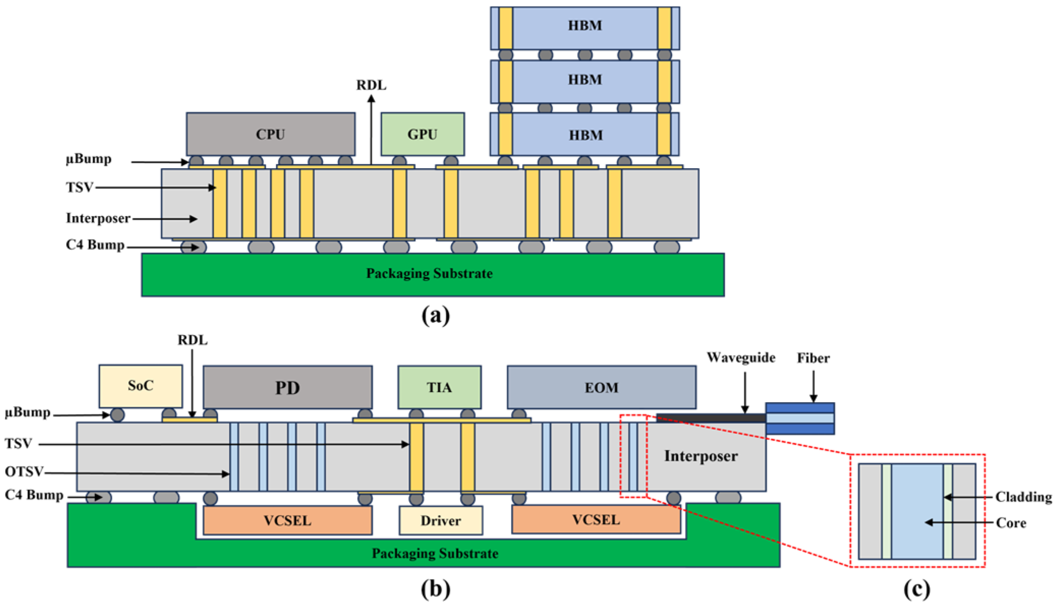
With the rapid and continuous advancement of artificial intelligence (AI) [1], high performance computing (HPC) [2], and 5G/6G technologies, there has been an increasing demand for enhanced chip performance, including bandwidth, latency, thermal dissipation, reliability, functionality, etc. However, the widely adopted electronic integrated circuit (EIC) architecture, i.e., metal-oxide-semiconductor field-effect transistors (MOSFETs) with metal-based electrical interconnects such as aluminum (Al) traces, intermetallic bumps, and copper (Cu)-metallized TSVs, has almost approached the scalability and capability limits. In this context, photonic integrated circuits (PICs) which typically comprise photodetectors (PDs), vertical cavity surface emitting lasers (VCSELs), electro-optic modulators (EOMs), optical waveguides, optical filters, combiners [3], splitters [4], etc., are considered to be a superior alternative to push these limits [5], thanks to their inherent advantages including low loss, high transmission speed, and optimal tolerance to electromagnetic interference [6,7]. In a three-dimensional (3D) EIC system, TSVs serve as the most efficient approach for electrical communication vertically, as shown in Figure 1a. Analogously, as given by Figure 1b, in a 3D PIC system, OTSVs act as the vertical light path between staked photonic chips [8]. Theoretically, they can be as straightforward as empty Si vias filled with nothing but air. However, despite the simplicity, the downside of such a configuration is the high loss [9,10], since the via sidewall is scalloped (due to Bosch Process’s nature) and light tends to penetrate Si [11]. One way to solve this issue is to coat the Si sidewall with a lower refractive index material (i.e., cladding) and fill the inner part with higher refractive index material (i.e., core), turning it into a vertical optical fiber where light can propagate by total internal reflection, as described by Figure 1c. Nevertheless, the scalloped unevenness cannot be eliminated from the Si sidewall and will be inherited by the cladding–core interface, therefore resulting in loss.
Figure 1.
Schematic demonstrations of (a) a typical EIC based on TSVs; (b) a typical PIC based on OTSVs; (c) a typical OTSV comprising core and cladding.
Over the last decade, significant efforts have been devoted to advancing the development of OTSVs. Muhannad Bakir et al. created a unique process to fabricate OTSV and TSV simultaneously [12,13], in which a ring-shaped region is first opened through deep reactive ion etching (DRIE) then filled with silicon oxide (SiO2) through physical vapor deposition (PVD) as the cladding. The remaining inner Si therefore serves as the core, which provides pronounced light confinement and supports an increased number of modes due to its inherently higher refractive index. Nevertheless, to achieve efficient mode matching, the ring region should be accurately opened and completely filled, thereby posing stringent requirements on the precision and reliability of the corresponding DRIE and PVD procedures. Yutaka Takagi et al. mechanically drilled through vias on printed circuit boards (PCBs) for electro-optic packaging [14,15]. Owing to the inherent surface roughness and limited mechanical rigidity of PCBs, together with the large form factor of the drill bit, these vias possess a relatively larger diameter. Bruce Chou et al. formed optical through-glass vias (OTGVs) based on laser ablation for vertical light transmission [16,17]. As a result of the inherent gradient in laser intensity, the resulting vias inevitably possess a sloped sidewall. Currently, the most widely adopted approach for TGV opening is laser-induced wet etching, which significantly reduces the risk of localized thermal damage in comparison with laser ablation. Nevertheless, owing to the gradient in hydrofluoric acid (HF) solution concentration within the via, combined with the double-sided etching mechanism, the resulting via is prone to exhibiting an X-shaped cross-section. Sebastian Killge et al. tested various core materials and fabricated low loss OTSVs [18,19]. Nevertheless, this work is mainly oriented towards the fabrication process development, whereas the fundamental transmission and coupling characteristics of the OTSV remain insufficiently understood. More critically, all these studies overlooked the influence of packaging imperfections, especially the misalignment of the light source to the via.
Therefore, to solve these challenges, we implement an optical-fiber-like OTSV model to investigate the effect of critical factors, including the cladding and core thickness and properties, via geometry and sidewall roughness on the transmission performance, which could be an effective guideline for the OTSV development.
2. Numerical Analysis
To ensure good cladding coverage and thickness uniformity, thermal silicon oxide (SiO2) with a refractive index (nclad) of 1.44 and a fixed thickness (tclad) of 1.5 μm is chosen as the cladding material. To balance fabrication complexity with transmission performance, SU-8 is used as the core material [20]. This polymer can be filled into the via rapidly through vacuum suction, followed by a standard curing procedure for solidification purposes. The height of the OTSV is fixed at 100 μm and three core diameter (dotsv) configurations, 10 μm, 20 μm and 30 μm, are evaluated. The incident light source is selected as a Gaussian-distributed beam with a wavelength λ0 of 1550 nm [21,22], the relevant half beam waist ω is therefore governed by Equation (1).
where ω0 is the initial half beam waist of the Gaussian beam, ncore denotes the refractive index of core (1.56), and z stands for the propagation distance from the emission source in the vertical direction. Typically, ω0 is defined as the radial distance at which the light intensity decays to 1/e of its on-axis value. Nevertheless, to capture the region outside this range and to simplify the calculation process, the emission source with a sidelength of 4ω0 is placed in direct contact with the bottom of the OTSVs (z = 0), which ensures the beam waist satisfies ω = ω0.
For propagation distances significantly greater than the wavelength (z >> λ0), ω can be simplified as
where θg represents the Gaussian beam divergence angle. During the simulation, the half beam width is set to vary to maximize mode matching with the OTSV, which leads the divergence angle to change accordingly. As a result, the resulting divergence angle different diameters may not be identical once the mode is successfully matched. With the radial distance from the beam center r, the beam intensity I and the beam energy E can be written as
where I0 is the central beam intensity and E0 is the total beam energy. The relationship between the number of guided modes Nm and normalized frequency V can be described as follows.
Owing to etching challenges in practice, the minimum attainable OTSV diameter is set to 10 μm, at which point V and Nm are 12 and 74, respectively. As a result, all OTSVs investigated in this study function as multimode waveguides.
To account for potential misalignment in the light pathway between two optical components (such as a laser generator and an electro-optical modulator) after manufacturing or packaging, four representative cases are investigated using the finite-difference time-domain (FDTD) method with a grid size of 0.15 μm and perfectly matched layer (PML) boundary condition in x, y, and z directions. The first involves a lateral offset between the beam axis and the core axis, which is noted as Δx, as shown in Figure 2a. For each OTSV diameter, the maximum Δx is equal to the via radius. Similarly, the second case is the incident angle deviation, which is noted as Δθ, as illustrated by Figure 2b. After that, with a higher aspect ratio, the via is more likely to have a sloped sidewall profile, i.e., a trapezoidal cross-section, as given by Figure 2c, since it is more difficult for the etchant and passivation chemicals to reach the via bottom. Hence, slope angles (noted as θs) from 0 to 3° are considered to represent realistic fabrication scenarios. In the last case, the core sidewall is scalloped to imitate the morphology inherent to the Bosch Process, as illustrated in Figure 2d. Specifically, the unevenness is assumed to be sinusoidal, with a peak–valley amplitude Rou ranging from 0.1 μm to 1 μm, and a peak–peak period Pr varying from 1 μm to 3 μm.
Figure 2.
Schematic demonstrations of four typical OTSV fabrication or package defeats: (a) lateral offset between the incident beam and the via; (b) angular tilt of the incident beam; (c) sloped sidewalls resulted from limited transport of etchant and the passivation agents to the far end; (d) sidewall roughness inherent to the repeated etch-passivation cycles of the Bosch Process.
3. Results and Discussion
The investigation is carried out in two stages. First, the beam width and the via diameter are optimized to find the optimal geometric condition that maximizes coupling efficiency and minimizes insertion loss. After that, three critical fabrication/packaging-induced imperfections, including beam–via misalignment, via sidewall slope and sidewall roughness, are investigated.
3.1. Effect of Light Beam Width and via Diameter
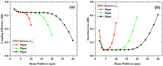
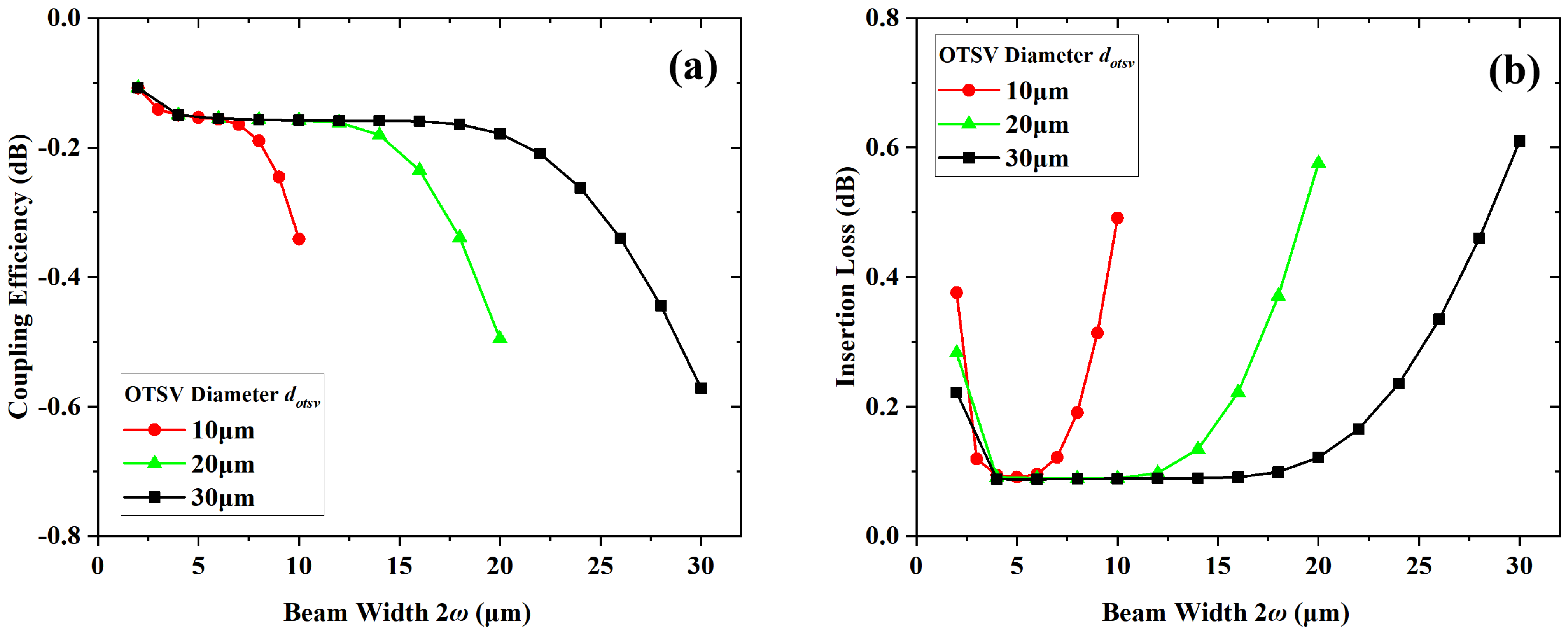
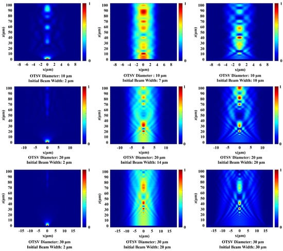
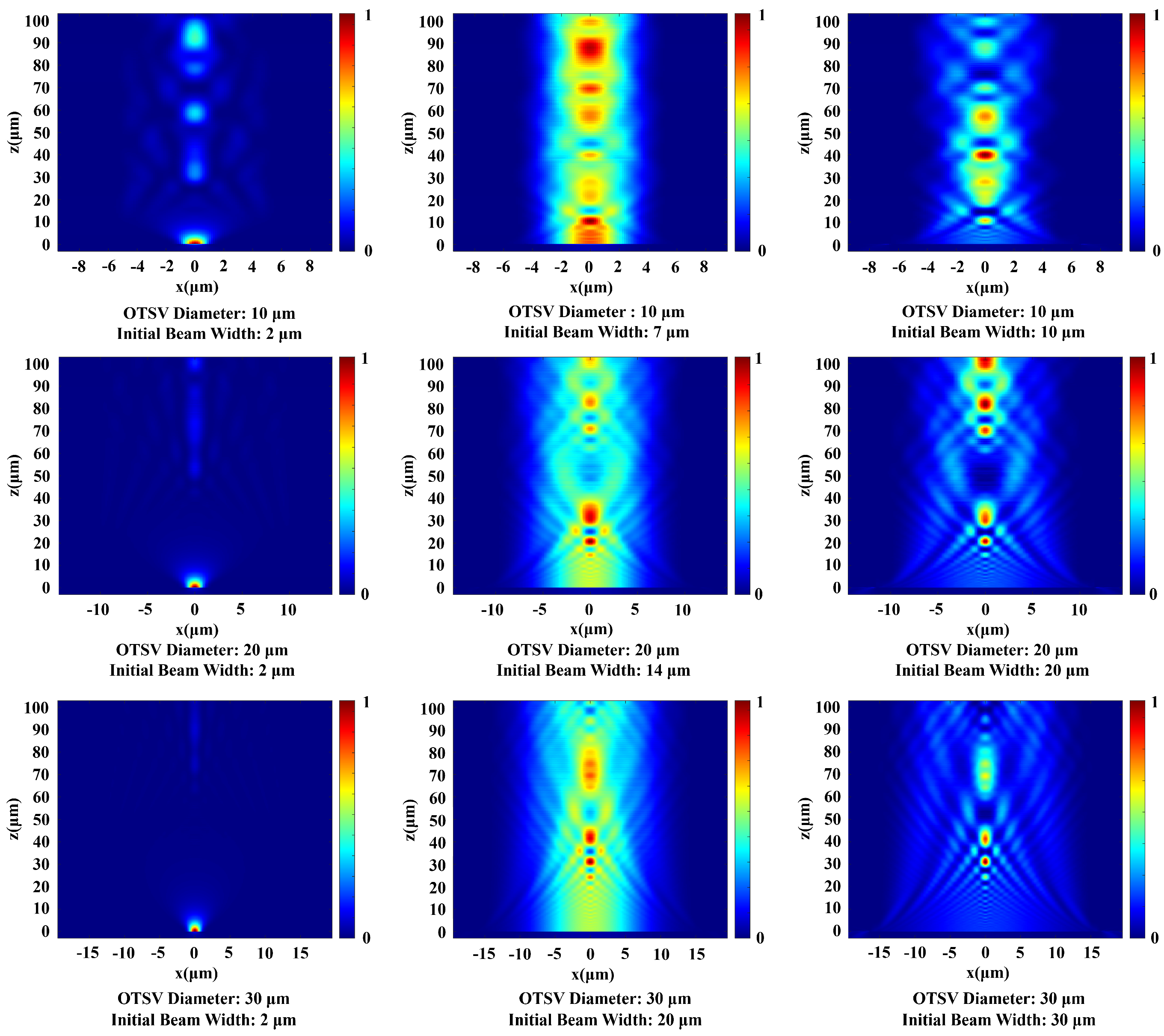
Two monitors with a width equal to the OTSV diameter are positioned at distances 1 μm and 100 μm above the OTSV bottom to evaluate the coupling efficiency and the insertion loss, respectively. As shown in Figure 3a, for all via diameters, as the beam width grows, the coupling efficiency initially declines rapidly, then stabilizes at approximately −0.16 dB, after which it witnesses a second significant downward trend. Similarly, the insertion loss drops sharply and stabilizes at 0.09 dB at first. Nevertheless, after that, it enters into a climbing trend instead. Specifically, if the beam width is smaller than dmo, the loss is dominated by beam divergence within the via. On the other hand, as the beam width exceeds dmo, light leakage into the sidewall becomes the predominant loss reason. The transition between divergence-dominant and leakage-dominant can be witnessed in the results in Figure 4.
Figure 3.
Effects of OTSV diameter and initial beam width on (a) coupling efficiency and (b) insertion loss.
Figure 4.
Light intensity distributions for various OTSV diameters and beam widths.
3.2. Effect of Misalignment
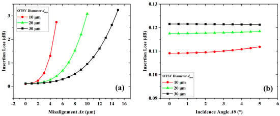
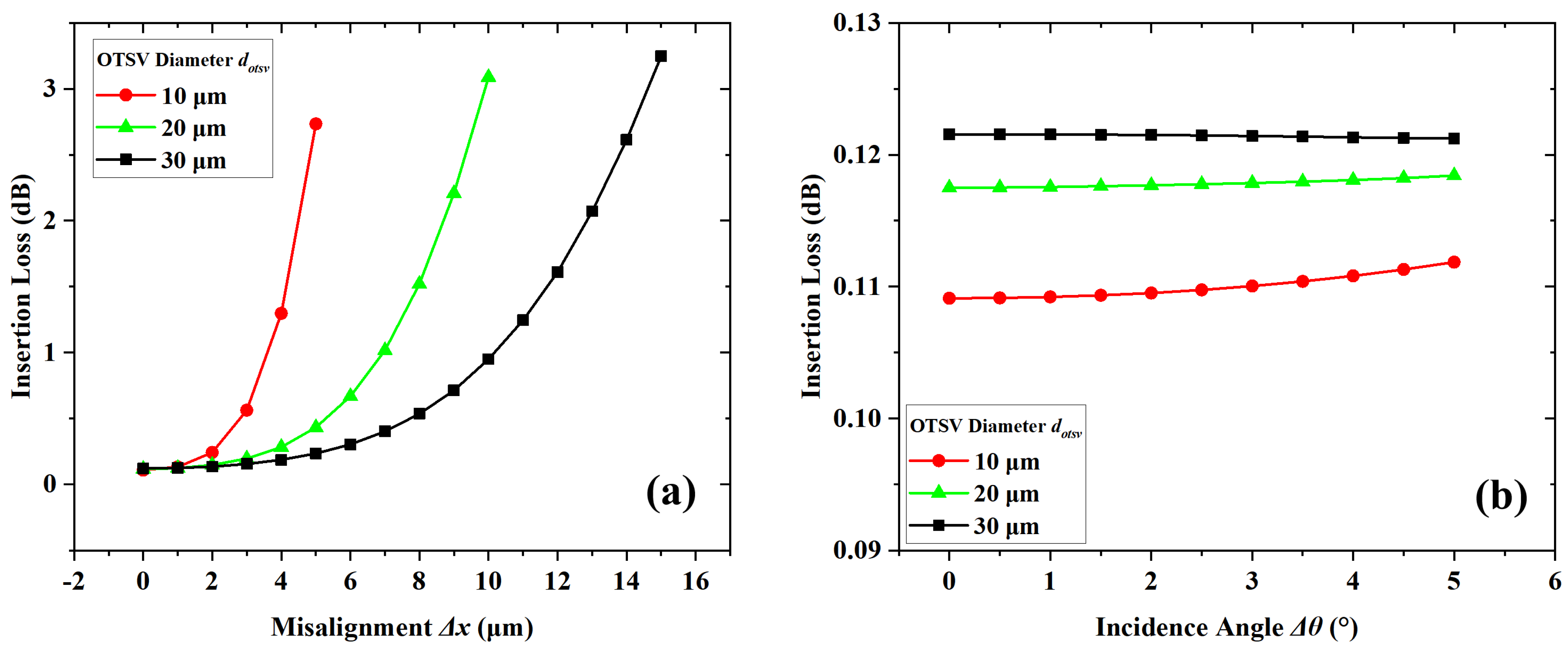
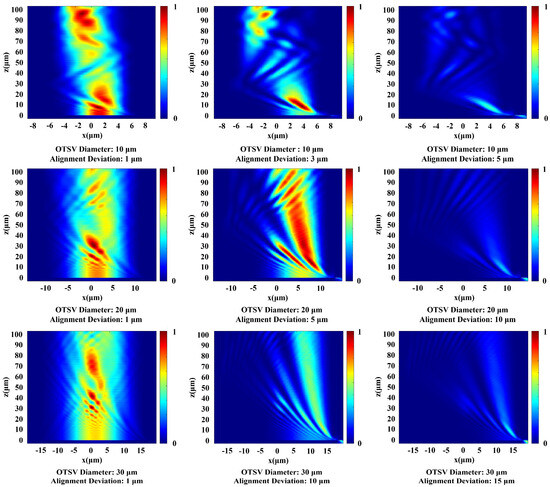
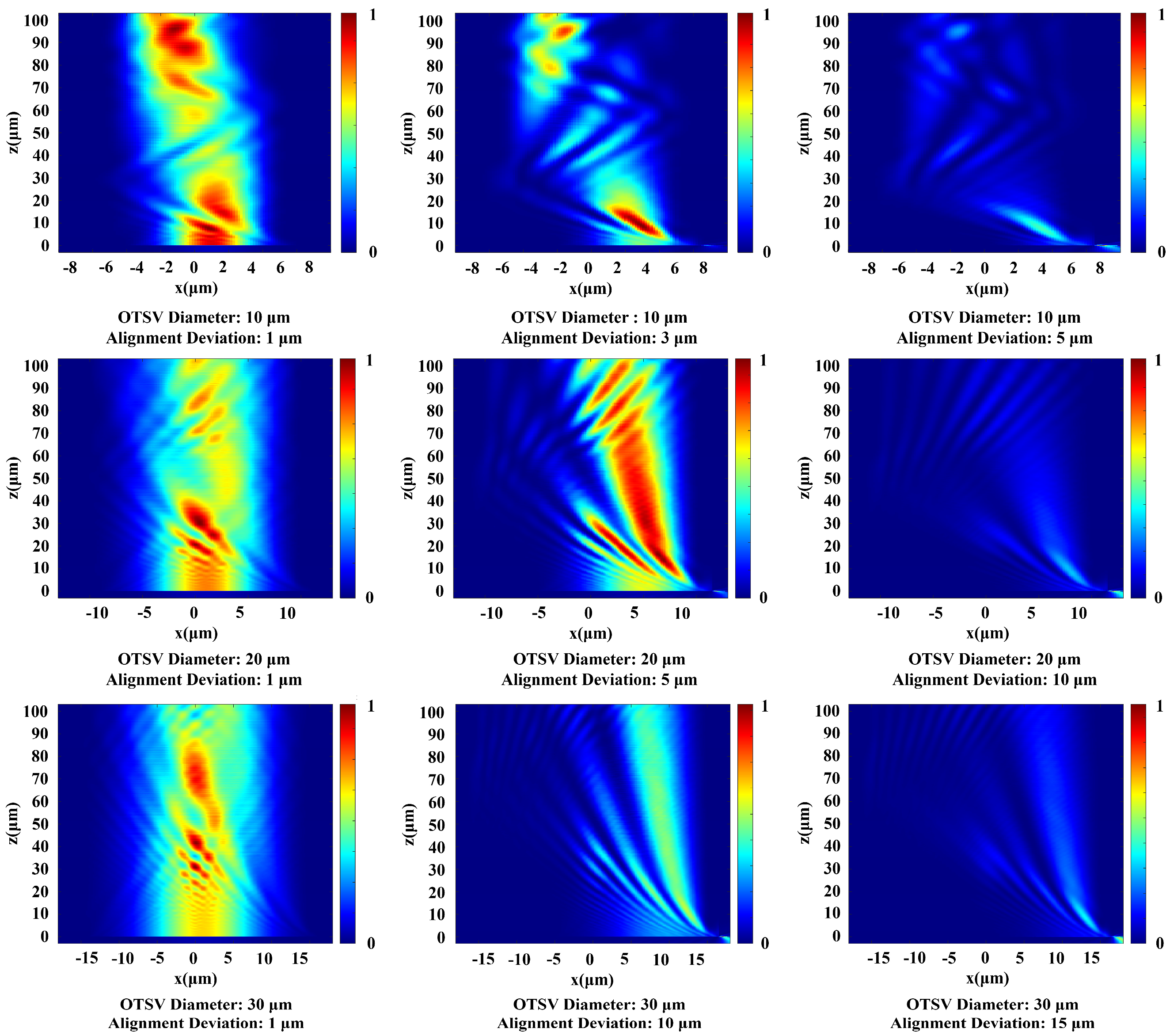
With increasingly severe beam–via axis misalignment, the insertion loss exhibits a steady growth across all via diameters. In addition, larger via diameters demonstrate reduced susceptibility to misalignment, which is reflected by its comparatively gradual increase, as illustrated in Figure 5a. This observation is further supported by the corresponding power distributions presented in Figure 6, which confirm that a larger via permits greater light energy transmission.
Figure 5.
Effects of OTSV diameter on insertion loss (a) with lateral misalignment; (b) with incidence angle misalignment.
Figure 6.
Light intensity distributions for various OTSV diameters and alignment deviations.
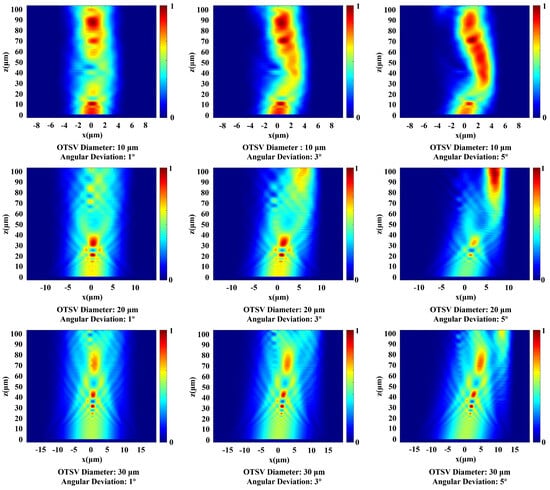
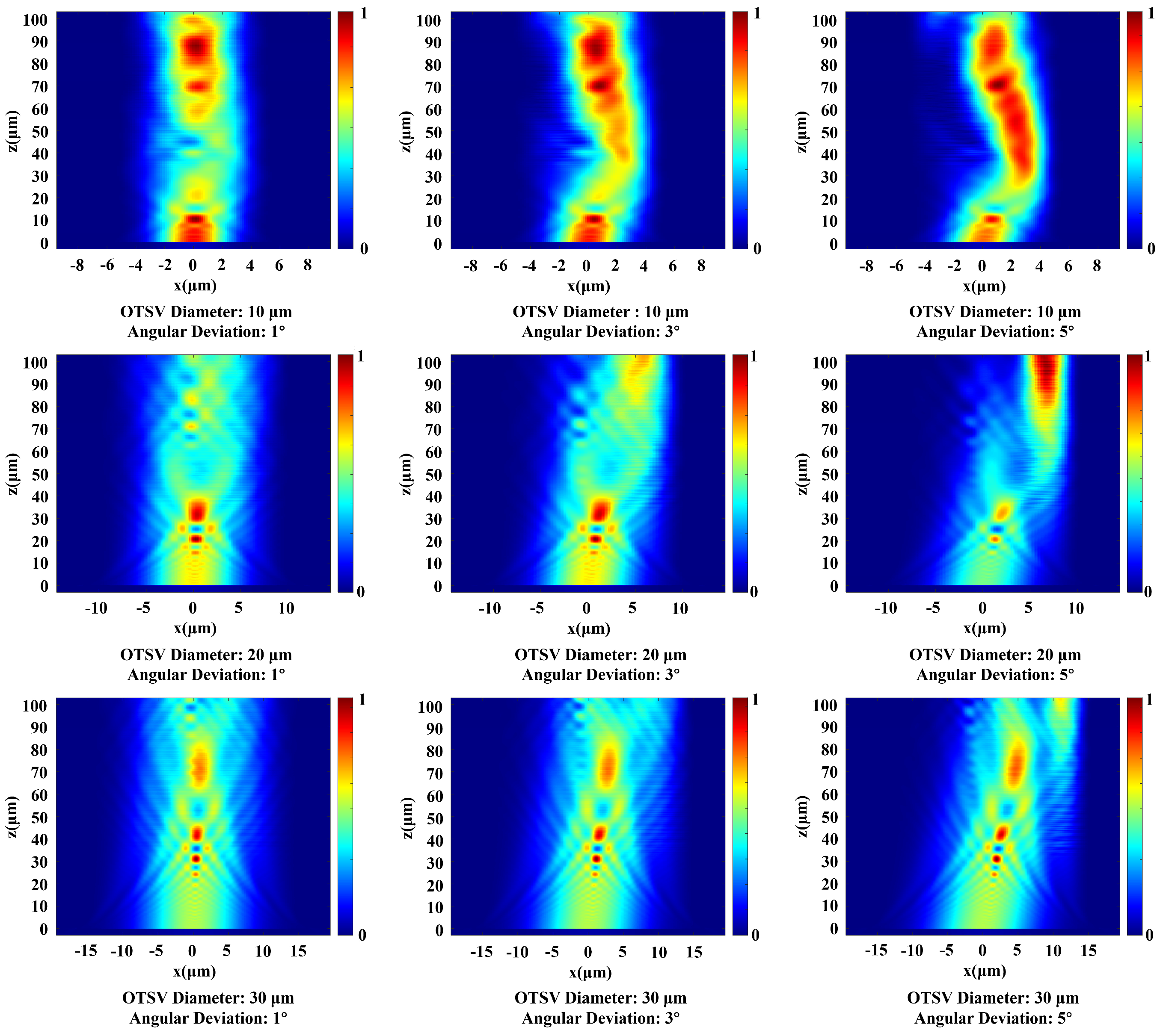
In contrast, from Figure 5b, the insertion loss exhibits a relatively mild dependence on increasing incident angle, since observable increases can barely be witnessed for via diameters of 20 µm and 30 µm. Apart from that, at any given incident angle, a larger via diameter leads to higher insertion loss. This phenomenon is ascribed to the increased number of higher-order modes provided by a larger diameter, which exacerbates the sidewall leakage loss. The energy distributions within the via, as presented in Figure 7, indicate that a larger via diameter consistently yields higher insertion loss, although they all shift accordingly with the incident angle misalignment. More importantly, a key implication of these findings is that, if the maximum detected power at via exit end occurs off-axis during practical alignment, one may conclude that the light source is not perpendicularly aligned with the via.
Figure 7.
Light intensity distributions for various OTSV diameters and alignment angles.
From the perspectives of alignment and bonding, active alignment systems, while capable of reducing the lateral and angular misalignments to 0.5 μm and 0.005° respectively in some cases, are limited to performing precise alignment only and incapable of executing the subsequent bonding step. In addition, the dynamic positioning and attitude adjustment process inherent to these systems is relatively time-consuming. As a result, passive pick-and-place packaging remains the predominant approach in laboratory prototyping or industrial mass production, which are generally associated with the lateral and angular misalignments of more than 4 μm and 0.02°, respectively [23,24,25,26,27,28,29]. In this context, OTSVs with a diameter of 10 or less are more susceptible to packaging-induced lateral misalignment, whereas the effect of angular misalignment is negligible.
3.3. Effect of Sidewall Slope
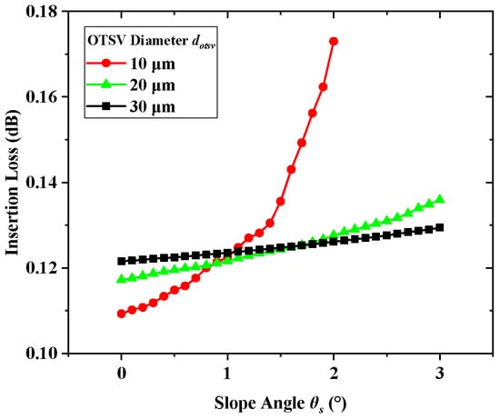
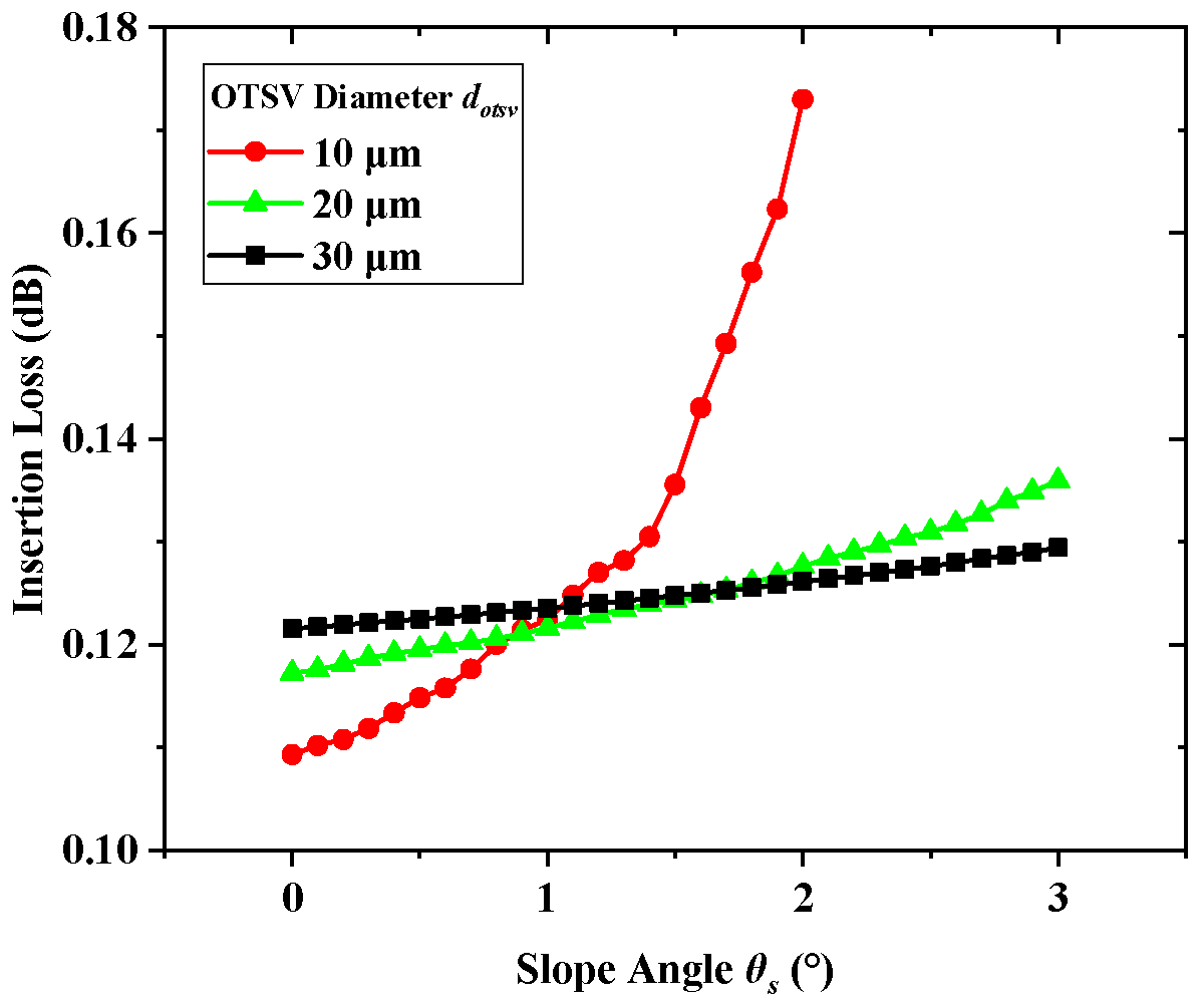
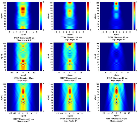
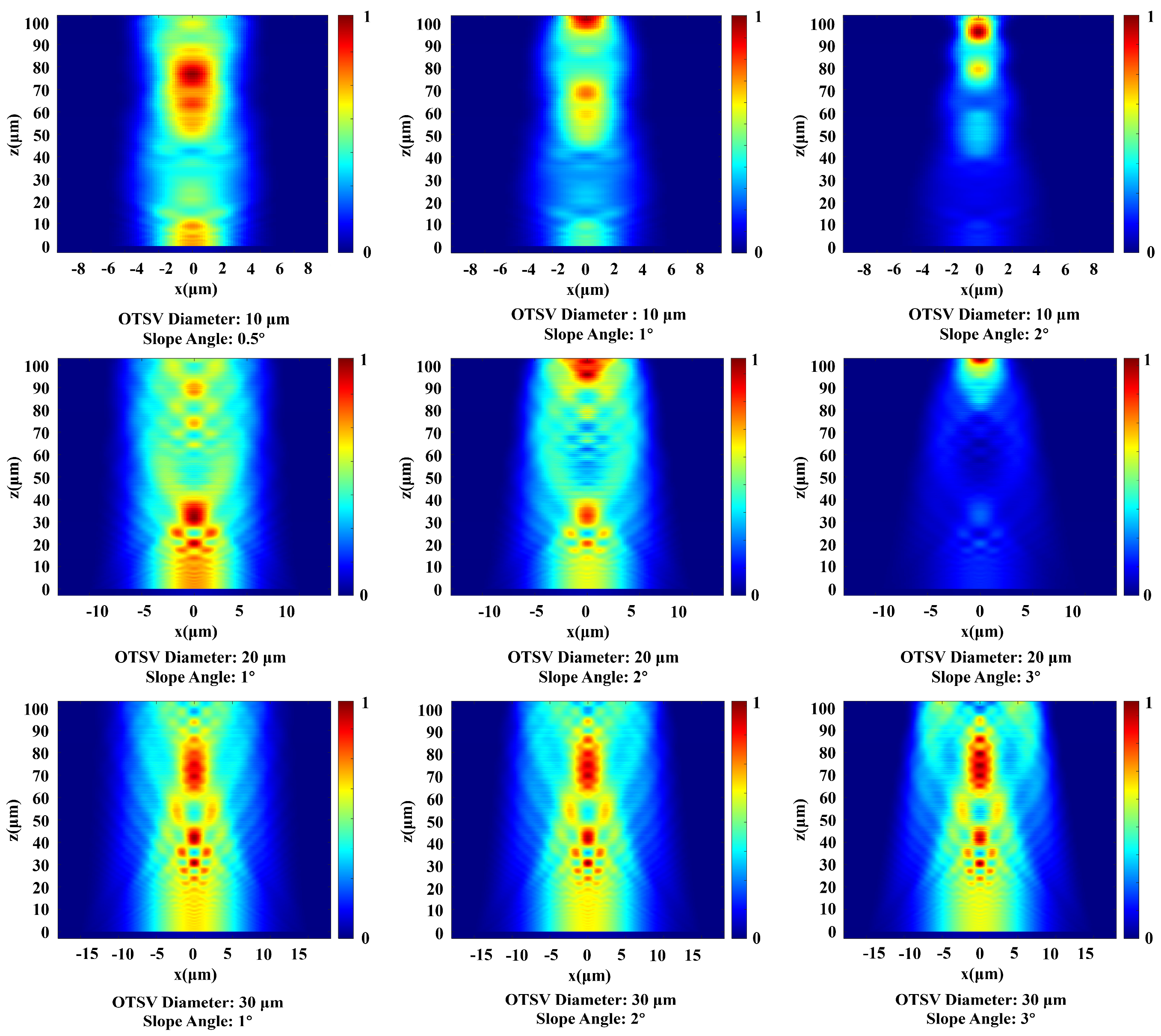
In this configuration, the via top diameter is adjusted accordingly with variations in the slope angle. The insertion loss exhibits a positive correlation with the sidewall slope angle θs, as demonstrated in Figure 8. Specifically, for slope angles below 1°, the insertion loss remains at a relatively low level of less than 0.13 dB for all vias. Nevertheless, the smallest via is more sensitive to a reduced via top, witnessing a sharp upward trend once θs exceeds approximately 1.4°. At an inclination angle of 2°, its top diameter shrinks to about 3 μm, effectively nearing closure. This geometric constriction is likely the primary contributor to the observed dramatic loss increase. Interestingly, the smallest via displays a substantial insertion loss increase of 0.065 dB, while the larger counterparts show limited sensitivity to the sidewall geometry variations, with a rise of about 0.01 dB. This observation suggests that improved light confinement enabled by wider structures helps mitigate mode field mismatch, which is confirmed by the energy distribution plots provided in Figure 9.
Figure 8.
Effects of OTSV diameter and misalignment on transmission loss.
Figure 9.
Light intensity distributions for various OTSV diameters and slope angles.
Collectively, the above findings underscore the importance of maintaining low sidewall slopes during the DRIE procedure to effectively minimize the insertion loss. However, the quality of the via sidewall profile deteriorates with increasing aspect ratio. Substantial optimization of the etchant formulation is typically necessary to achieve a slope angle below 1°. Therefore, a more pragmatic approach is to reduce the aspect ratio either by enlarging the via diameter or by decreasing the via depth, which thereby relaxes the fabrication constraints.
Furthermore, it should be noted that spot-size converters (SSCs) represent a well-established solution that leverages tapered geometries to minimize or eliminate mode mismatch [30]. To extend this horizontal configuration to vertical OTSVs, the via should first be formed with a sloped sidewall profile, followed by the growth of a conformal SiO2 cladding layer on the sidewall. Lastly, the inner core region should be completely filled with low-loss silicon nitride (Si3N4) using chemical vapor deposition (CVD). However, at present, such a proposed process flow is not feasible, owing to two principal fabrication constraints. First, the achievable taper angle (i.e., via sidewall slope angle) and the overall sidewall quality of the via are unlikely to meet the demanding specifications routinely achieved in horizontal SSCs. Second, the core region is too large to be effectively filled with CVD Si3N4, which would likely result in poor deposition uniformity and consequently increased optical loss.
3.4. Effect of Sidewall Roughness
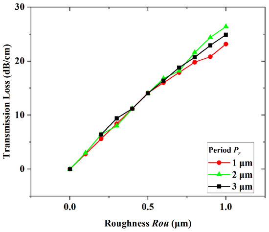
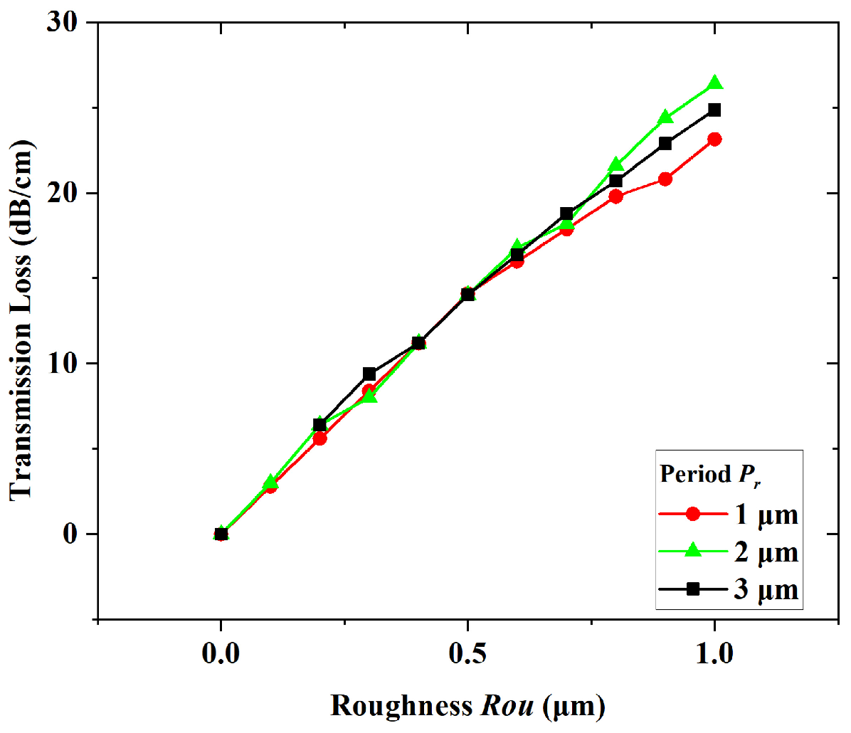
For typical optical waveguides, the ridge sidewall quality critically determines their light transmission efficiency, as surface unevenness might lead to light scattering [31,32]. This fundamental principle also governs the OTSV performance. Unfortunately, considering the etching mechanism of Bosch Process, scalloped morphology on the via sidewall can hardly be eliminated. As clearly shown in Figure 10, transmission losses for periods of 1 μm, 2 μm and 3 μm are almost the same and grow linearly from 0 to 0.5 μm. Beyond that point, structures with shorter periods (1 μm) demonstrate marginally lower loss accumulation rates. Since one scallop corresponds to an individual etch cycle, increasing the switching frequency between the etch and passivation steps is advantageous for minimizing scallop formation on the sidewall in theory. However, this approach places significant demands on equipment performance and long-term operational stability. A more viable alternative, therefore, is to optimize the precursor formulation to suppress lateral etching, followed by repeated thermal oxidation and subsequent hydrofluoric acid (HF) wet etching of SiO2 to further smooth the sidewall [33,34,35].
Figure 10.
Effects of sidewall roughness periods and peak–valley amplitudes on transmission loss.
4. Conclusions
This study systematically investigates the impact of light beam and via structural properties on OTSV transmission performance. Optimal coupling is achieved when the beam width is in a certain range, balancing divergence-induced loss and sidewall leakage. Among the fabrication and packaging imperfections examined, lateral misalignment and sidewall slope exert the most pronounced influence on transmission loss. Specifically, larger diameter vias demonstrate superior tolerance to both lateral offset and angular deviation. Smaller diameter vias are noticeably more sensitive to sidewall slope variations. Furthermore, transmission loss is exacerbated by sidewall irregularities. Thus, beyond shortening Bosch cycle durations, optimizing the precursor chemistry to reduce lateral etching and applying a post-wet etch could be advantageous.
Meanwhile, several limitations should be acknowledged. The current model assumes fixed via height, perfect material homogeneity, and ideal Gaussian beam illumination. Practical fabrication processes may introduce height variations, non-uniform sidewall profiles, and material inhomogeneity. Additionally, coupling from actual sources such as VCSELs or integrated waveguides may exhibit more complex mode characteristics than the Gaussian approximation employed here. Future work will incorporate experimentally derived statistical models for sidewall roughness and realistic source profiles to enhance predictive accuracy. Nevertheless, the qualitative trends and relative importance of fabrication parameters identified in this study provide a robust foundation for OTSV optimization in practical manufacturing contexts.
Author Contributions
Conceptualization, B.H. and S.X.; methodology, S.X.; software, B.H. and F.C.; validation B.H. and Y.Q.; formal analysis, B.H. and S.X.; investigation, B.H. and Y.Q.; resources, Y.Q.; data curation, B.H. and F.C.; writing—original draft preparation, B.H. and Y.Q.; writing—review and editing, Y.D. and Y.Q.; visualization, Y.D. and Q.Z.; supervision, Y.Q. and T.H.; project administration, Y.Q. and T.H.; funding acquisition, S.Z., X.Z., Y.Q., Q.Z. and T.H. All authors have read and agreed to the published version of the manuscript.
Funding
This research was funded in part by the National Key Research and Development Program of China under Grant 2024YFA1209100, in part by the State Key Laboratory of Radio Frequency Heterogeneous Integration under Grant KF2024004, in part by the Research Program of Shanghai under Grants 25TS1410400 and 24JD1401800, in part by the Shanghai Municipal Key Program for Fundamental Research in Integrated Circuits under grant 25JD1403700, in part by the National Natural Science Foundation of China under Grants 62204149 and 62575166.
Data Availability Statement
The datasets generated during and/or analyzed during the current study are available from the corresponding authors on request.
Conflicts of Interest
The authors declare no conflicts of interest.
References
- Bandi, A. A Review Towards AI Empowered 6G Communication Requirements, Applications, and Technologies in Mobile Edge Computing. In Proceedings of the 2022 6th International Conference on Computing Methodologies and Communication (ICCMC), Erode, India, 29–31 March 2022; pp. 12–17. [Google Scholar]
- Ashari, A.; Riasetiawan, M. High Performance Computing on Cluster and Multicore Architecture. TELKOMNIKA (Telecommun. Comput. Electron. Control) 2015, 13, 1408–1413. [Google Scholar] [CrossRef] [Scilit]
- Smolanski, S.S.; Malka, D. O-Band 4 × 1 Combiner Based on Silicon MMI Cascaded Tree Configuration. Micromachines 2025, 17, 31. [Google Scholar] [CrossRef] [Scilit] [PubMed]
- Ioudashkin, E.; Malka, D. High-Performance O-Band Angled Multimode Interference Splitter with Buried Silicon Nitride Waveguide for Advanced Data Center Optical Networks. Photonics 2025, 12, 322. [Google Scholar] [CrossRef] [Scilit]
- Bashir, J.; Peter, E.; Sarangi, S.R. A Survey of On-Chip Optical Interconnects. ACM Comput. Surv. 2019, 51, 1–34. [Google Scholar] [CrossRef] [Scilit] [PubMed]
- Lancaster, A.; Keswani, M. Integrated circuit packaging review with an emphasis on 3D packaging. Integration 2018, 60, 204–212. [Google Scholar] [CrossRef] [Scilit]
- Cho, D.H.; Seo, S.M.; Kim, J.B.; Rajendran, S.H.; Jung, J.P. A Review on the Fabrication and Reliability of Three-Dimensional Integration Technologies for Microelectronic Packaging: Through-Si-via and Solder Bumping Process. Metals 2021, 11, 1664. [Google Scholar] [CrossRef] [Scilit]
- Takagi, Y.; Suzuki, A.; Horio, T.; Ohno, T.; Kojima, T.; Takada, T.; Iio, S.; Obayashi, K.; Okuyama, M. 4-Ch × 10-Gb/s Chip-to-Chip Optical Interconnections with Optoelectronic Packages and Optical Waveguide Separated from PCB. In Proceedings of the 2010 IEEE CPMT Symposium Japan, Tokyo, Japan, 24–26 August 2010; pp. 1–4. [Google Scholar]
- Villasmunta, F.; Steglich, P.; Schrader, S.; Schenk, H.; Mai, A. Numerical Simulation of Optical Through-Silicon Waveguide for 3D Photonic Interconnections. In Proceedings of the 2021 International Conference on Numerical Simulation of Optoelectronic Devices (NUSOD), Turin, Italy, 13–17 September 2021; pp. 115–116. [Google Scholar]
- Villasmunta, F.; Steglich, P.; Villringer, C.; Schrader, S.; Schenk, H.; Mai, A.; Regehly, M. Design, fabrication, and characterization of integrated optical through-silicon waveguides for 3D photonic interconnections. In Proceedings of the SPIE OPTO, San Francisco, CA, USA, 11 March 2024. [Google Scholar]
- Huff, M. Recent Advances in Reactive Ion Etching and Applications of High-Aspect-Ratio Microfabrication. Micromachines 2021, 12, 991. [Google Scholar] [CrossRef] [Scilit] [PubMed]
- Noriki, A.; Lee, K.-W.; Bea, J.; Fukushima, T.; Tanaka, T.; Koyanagi, M. Through Silicon photonic via (TSPV) with Si core for low loss and high-speed data transmission in opto-electronic 3-D LSI. In Proceedings of the 2010 IEEE International 3D Systems Integration Conference (3DIC), Munich, Germany, 16–18 November 2010; pp. 1–4. [Google Scholar]
- Parekh, M.S.; Thadesar, P.A.; Bakir, M.S. Electrical, optical and fluidic through-silicon vias for silicon interposer applications. In Proceedings of the 2011 IEEE 61st Electronic Components and Technology Conference (ECTC), Lake Buena Vista, FL, USA, 31 May–3 June 2011; pp. 1992–1998. [Google Scholar]
- Takagi, Y.; Suzuki, A.; Horio, T.; Ohno, T.; Kojima, T.; Takada, T.; Iio, S.; Obayashi, K.; Okuyama, M. Optoelectronic Package having Optical Waveguide Hole and 4-ch × 10-Gb/s Chip-to-Chip Interconnection using Thin-film Waveguide Connector. In Proceedings of the Optical Fiber Communication Conference and National Fiber Optic Engineers Conference, San Diego, CA, USA, 22–26 March 2009. [Google Scholar]
- Takagi, Y.; Suzuki, A.; Horio, T.; Ohno, T.; Kojima, T.; Takada, T.; Iio, S.; Obayashi, K.; Okuyama, M. Optical Through-Hole with High Aspect Ratio for On-Board Optical Transmission. In Proceedings of the Optical Fiber Communication Conference/National Fiber Optic Engineers Conference 2011, Los Angeles, CA, USA, 6 March 2011; p. JWA085. [Google Scholar]
- Chou, B.C.; Sato, Y.; Sukumaran, V.; Sun, J.; Sundaram, V.; Chang, G.-K.; Tummala, R. Modeling, design, and fabrication of ultra-high bandwidth 3D Glass Photonics (3DGP) in glass interposers. In Proceedings of the 2013 IEEE 63rd Electronic Components and Technology Conference, Las Vegas, NV, USA, 28–31 May 2013; pp. 286–291. [Google Scholar]
- Chou, B.C.; Razdan, S.; Zhang, H.; Sun, J.; Bowen, T.; Smet, V.; Chang, G.-K.; Sundaram, V.; Tummala, R. Modeling, design, and demonstration of ultra-miniaturized and high efficiency 3D glass photonic modules. In Proceedings of the 2014 IEEE 64th Electronic Components and Technology Conference (ECTC), Lake Buena Vista, FL, USA, 27–30 May 2014; pp. 1054–1059. [Google Scholar]
- Killge, S.; Charania, S.; Richter, K.; Neumann, N.; Al-Husseini, Z.; Plettemeier, D.; Bartha, J.W. Realization of optical multimode TSV waveguides for Si-Interposer in 3D-chip-stacks. Proc. SPIE 2017, 10232. [Google Scholar] [CrossRef] [Scilit]
- Charania, S.; Neumann, N.; Killge, S.; Winkler, F.; Al-Husseini, Z.; Szilagyi, L.; Henker, R.; Ellinger, F.; Plettemeier, D.; Bartha, J.W. Design, Fabrication, and Comparison of 3D Multimode Optical Interconnects on Silicon Interposer. J. Light. Technol. 2020, 38, 3454–3460. [Google Scholar] [CrossRef] [Scilit]
- Neumann, N.; Charania, S.; Killge, S.; al-Husseini, Z.; Henker, R.; Ellinger, F.; Bartha, J.; Plettemeier, D. Modeling and characterization of optical TSVs. In Proceedings of the 17th Conference on Optical Fibres and Their Applications, Supraśl, Poland, 23–27 January 2017; Volume 10325. [Google Scholar] [CrossRef] [Scilit]
- Joyce, W.B.; DeLoach, B.C. Alignment of Gaussian beams. Appl. Opt. 1984, 23, 4187–4196. [Google Scholar] [CrossRef] [Scilit] [PubMed]
- Alda, J. Laser and Gaussian Beam Propagation and Transformation. In Encyclopedia of Optical and Photonic Engineering (Print)—Five Volume Set; CRC Press: Boca Raton, FL, USA, 2015; Volume 999, pp. 1193–1207. [Google Scholar]
- Wu, B.; Zhang, S.; Wang, F.; Chen, Z. Micro Copper Pillar Interconnection Using Thermosonic Flip Chip Bonding. J. Electron. Packag. 2018, 140, 044502. [Google Scholar] [CrossRef] [Scilit]
- Matsumoto, T.; Kurahashi, T.; Konoike, R.; Suzuki, K.; Tanizawa, K.; Uetake, A.; Takabayashi, K.; Ikeda, K.; Kawashima, H.; Akiyama, S.; et al. Hybrid-Integration of SOA on Silicon Photonics Platform Based on Flip-Chip Bonding. J. Light. Technol. 2019, 37, 307–313. [Google Scholar] [CrossRef] [Scilit]
- Theurer, M.; Moehrle, M.; Sigmund, A.; Velthaus, K.O.; Oldenbeuving, R.M.; Wevers, L.; Postma, F.M.; Mateman, R.; Schreuder, F.; Geskus, D.; et al. Flip-Chip Integration of InP and SiN. IEEE Photonics Technol. Lett. 2019, 31, 273–276. [Google Scholar] [CrossRef] [Scilit]
- Lee, J.; Lee, J.Y.; Song, J.; Sim, G.; Ko, H.; Kong, S.H. Implementation of Flip-Chip Microbump Bonding between InP and SiC Substrates for Millimeter-Wave Applications. Micromachines 2022, 13, 1072. [Google Scholar] [CrossRef] [Scilit] [PubMed]
- Baranowski, S.; Nguyen, A.; Hossain, M.J.; Kruger, S.; Carpenter, L.G.; Dikshit, A.; McDonough, C.; Harame, D.L. Heterogeneous Integration of III-V Lasers in a 300 mm CMOS Manufacturing Line. IMAPSource Proc. 2023, 2022, 465–469. [Google Scholar] [CrossRef] [Scilit]
- Yu, S.; Gaylord, T.K.; Bakir, M.S. Quarter-Micron Alignment of Chiplets via Positive Self-Aligned Structures. IEEE Photonics Technol. Lett. 2023, 35, 1183–1185. [Google Scholar] [CrossRef] [Scilit]
- Lu, M.-C. Hybrid Bonding for Ultra-High-Density Interconnect. J. Electron. Packag. 2024, 146, 030802. [Google Scholar] [CrossRef] [Scilit]
- Brunetti, G.; Heuvink, R.; Schreuder, E.; Armenise, M.N.; Ciminelli, C. Silicon Nitride Spot Size Converter with Very Low-Loss Over the C-Band. IEEE Photonics Technol. Lett. 2023, 35, 1215–1218. [Google Scholar] [CrossRef] [Scilit]
- Lee, K.K.; Lim, D.R.; Luan, H.-C.; Agarwal, A.; Foresi, J.; Kimerling, L.C. Effect of size and roughness on light transmission in a Si/SiO2 waveguide: Experiments and model. Appl. Phys. Lett. 2000, 77, 1617–1619. [Google Scholar] [CrossRef] [Scilit]
- Lee, K.K.; Lim, D.R.; Kimerling, L.C.; Shin, J.; Cerrina, F. Fabrication of ultralow-loss Si/SiO2 waveguides by roughness reduction. Opt. Lett. 2001, 26, 1888–1890. [Google Scholar] [CrossRef] [Scilit] [PubMed]
- Park, J.S.; Kang, D.-H.; Kwak, S.M.; Kim, T.S.; Park, J.H.; Kim, T.G.; Baek, S.-H.; Lee, B.C. Low-temperature smoothing method of scalloped DRIE trench by post-dry etching process based on SF6 plasma. Micro Nano Syst. Lett. 2020, 8, 14. [Google Scholar] [CrossRef] [Scilit]
- Wang, Y.; Chen, L.; Zeng, X.; Song, J. A Modified Bosch Process of SF6/C4F8/O2 ICP-RIE Si Etching. J. Mater. Eng. Perform. 2024, 34, 17472–17478. [Google Scholar] [CrossRef] [Scilit]
- Syed Mohammed, Z.A.; Olimpo, M.A.S.; Poenar, D.P.; Aditya, S. Smoothening of scalloped DRIE trench walls. Mater. Sci. Semicond. Process. 2017, 63, 83–89. [Google Scholar] [CrossRef] [Scilit]


Disclaimer/Publisher’s Note: The statements, opinions and data contained in all publications are solely those of the individual author(s) and contributor(s) and not of MDPI and/or the editor(s). MDPI and/or the editor(s) disclaim responsibility for any injury to people or property resulting from any ideas, methods, instructions or products referred to in the content. |
© 2026 by the authors. Licensee MDPI, Basel, Switzerland. This article is an open access article distributed under the terms and conditions of the Creative Commons Attribution (CC BY) license.