


Abstract
This work presents a comprehensive analytical and simulation-based comparison between bulk-driven (BD) and gate-driven (GD) operational transconductance amplifiers (OTAs) operating in the deep-subthreshold ultra-low-voltage regime. While BD techniques are traditionally considered unsuitable for high-performance analog design due to their lower transconductance efficiency, this study demonstrates that, when combined with self-cascode structures, BD architectures achieve competitive intrinsic gain, enhanced input common-mode range, and improved slew rate efficiency under nanoampere bias conditions. To support these claims, closed-form analytical derivations, dynamic analysis, and comprehensive Monte Carlo and PVT simulations are provided to quantify robustness and mismatch sensitivity. The results establish a systematic framework for evaluating BD versus GD architectures under identical technology and power constraints, offering practical design guidelines and optimized self-cascoded topologies for next-generation energy-autonomous systems.
1. Introduction
The relentless demand for energy-autonomous electronic devices within the frameworks of the Internet of Things (IoT) [1], wearable, biomedical, and implantable microsystems [2,3,4,5,6], and even in sectors not traditionally related, such as automotive electronics [7], continues to grow. As a result, analog integrated circuit (IC) design has been pushed toward the deep ultra-low-voltage (ULV) and ultra-low-power (ULP) frontiers. Operating circuits with supply voltages (VDD) significantly below 1 V, often approaching or even falling below the threshold voltage (Vth) of the CMOS process, with current consumption in the range of a few nanoamperes, is no longer a niche requirement. Such operation is necessary to maximize battery longevity and enable operation from purely energy-harvested sources.
In this framework, conventional gate-driven (GD) MOS configurations in strong inversion (SI) face severe headroom limitations. Since the gate-to-source voltage (VGS) must exceed Vth to maintain sufficient inversion levels, the input common-mode range (ICMR) becomes severely constrained [8]. To mitigate these limitations, operating devices in the subthreshold (specifically, weak inversion, WI) regime is particularly advantageous. This approach allows for a significant reduction in the required overdrive voltage while maximizing the transconductance-to-current (gm/ID) ratio [9]. In this region, the MOS transistor behavior shifts from a square-law dependency to an exponential relationship, effectively mimicking the operation of a bipolar junction transistor. However, even in the subthreshold, GD implementations remain “voltage constrained.” Consider, for instance, a standard n-type differential pair, M1-M2, with a tail current source M3. The minimum input common-mode voltage ensuring saturation of the transistor implementing the tail current generator is limited by VICM,min = VGS1,2 + VDS3,sat.
In ULV designs where VDD is scaled down to 500 mV or less, this requirement can consume nearly the entire supply rail, limiting the input signal to a narrow window near VDD and leaving zero headroom for signal swings. While complementary parallel p- and n-type structures can achieve rail-to-rail operation, they introduce significant complexity and the challenge of maintaining a constant total transconductance [8,10].
To circumvent these topological bottlenecks, the bulk-driven (BD) (a.k.a. body-driven) technique has emerged as a compelling alternative [11,12,13,14,15]. By applying the signal to the body terminal, the Vth requirement is effectively decoupled from the signal path, allowing for rail-to-rail or even supra-rail ICMR. This represents a fundamental shift from a voltage-limited path to a current-modulated path, where the bulk terminal acts as a secondary gate with no DC voltage requirement relative to channel formation, thereby enabling true deep ULV functionality that remains robust even as Vth exceeds VDD.
Despite these potential advantages, the BD approach is often regarded as unsuitable for high-performance analog VLSI applications and still receives limited acceptance in industrial practice. This perception stems from the inherently lower transconductance associated with the bulk terminal (gmb is approximately 0.1–0.25 times gm) and concerns regarding device modeling, robustness and reliability. Indeed, the bulk terminal was historically treated as a parasitic back-gate for which PVT (Process, Voltage, and Temperature) modeling accuracy was considered inferior to that of gate-driven operation. Additional drawbacks include the need for accessible bulk terminals (requiring triple-well or independent-well technologies), potential latch-up phenomena, and the need to avoid forward-biasing the bulk–source junction. However, several of the aforementioned issues have been progressively addressed, as demonstrated in the recent literature, including the recent work by the authors [15]. In particular, advances in processes, device modeling, circuit technologies and layout strategies have shown that bulk-driven implementations can achieve performance and robustness levels compatible with practical ULV-ULP (low-frequency) analog applications. Moreover, supply voltages below 0.4 V prevent significant forward-biasing of the body–source junction, thereby inherently avoiding latch-up.
Nevertheless, while several works have explored BD and GD amplifiers separately, a rigorous head-to-head comparative framework based on the same technology and comparable power budgets is still lacking. Building upon these premises, this paper presents an extensive and systematic analytical comparison between a BD OTA and a comparable GD counterpart, extending previous preliminary communication by the authors [16]. Both designs leverage the self-cascode (SC) structure to significantly enhance the intrinsic gain by providing a very high output resistance, thereby compensating for the reduced transconductance of the BD stage [17,18,19]. Specifically, the new contributions of this work include the following:
- A detailed analytical derivation of the self-cascode gain enhancement in subthreshold BD vs. GD stages, providing formal design equations for ULV operation.
- An expanded investigation into dynamic performance, demonstrating how the lower compensation requirements of BD OTAs can lead to a superior slew rate (SR) while maintaining comparable CMRR and PSRR.
- A comprehensive sensitivity analysis including Monte Carlo simulations for mismatch and PVT variations, quantifying the robustness of both architectures in deep-subthreshold regimes.
The paper is organized as follows: Section 2 describes the theoretical background of subthreshold operation. Section 3 explains the self-cascode structure, whereas Section 4 describes the architectural implementations of GD and BD designs using SC. Section 5 provides a formal theoretical comparison of the small-signal, large-signal and noise parameters. Section 6 discusses the pre-layout simulation results, corners and PVT simulation results, while Section 7 draws the final conclusions.
2. Theoretical Background
To accurately compare GD and BD architectures in the ULV regime, the physical behavior of the MOS transistor in weak inversion [20,21,22] must be first characterized. In the subthreshold region, the drain current, ID, is dominated by diffusion rather than drift, as expressed in (1):
where ID0 is the process-dependent current at VGS = Vth0, W/L is the aspect ratio, VT = kT/q is the thermal voltage (T is the absolute temperature, k is the Boltzmann constant, and q is the charge of the electron), and n is the subthreshold slope factor. Parameter n represents the nonideal capacitive coupling between the gate voltage and the channel surface potential equal to (1 + Cdep/Cox), and usually ranges from 1.2 to 1.4 in standard CMOS processes. For a device operating in subthreshold saturation (VDS ≥ 3VT ~ 4VT with good approximation), the term in parentheses approaches unity in (1), so that the drain current can be expressed as
where IS = ID0 (W/L).
To ensure operation in the weak inversion region, where the gm/ID (gm is the gate transconductance) ratio reaches its maximum and remains approximately constant, the following condition is imposed:
As is well known, at room temperature (300 K), 4VT is approximately 100 mV. For lower values of VGS (VGS < Vth0 − 4VT), we enter the deep-subthreshold region, which should be avoided because device mismatch increases, leakage currents become comparable to ID, and mobility degradation and trap effects appear.
We can also evaluate, from (2), the small-signal gate and bulk transconductances in weak inversion:
For comparison purposes, Table 1 summarizes the primary analytical differences between strong and weak inversion regimes.
Table 1.
Comparison of MOS parameters: strong vs. weak inversion.
In strong inversion, η represents the ratio of the bulk transconductance gmb to the gate transconductance gm, and is given as
While the analytical expressions for gm and gmb differ between inversion regions due to the dominant transport mechanisms (drift vs. diffusion in strong and weak inversion, respectively), the ratio gmb/gm remains physically linked to the capacitive coupling between the gate and the bulk. In both cases, this ratio is a direct manifestation of the substrate sensitivity, numerically represented by the term (n − 1) or η. In strong inversion, the depletion capacitance Cdep is defined as
Since , substituting this into Equation (6) yields
Therefore,
Since n is typically between 1.2 and 1.4, the value of η is typically between 0.2 and 0.4. Both in SI and WI, the bulk is then less effective at controlling the channel than the gate, but driving the MOS from the bulk remains the only solution when we want to circumvent the threshold-limited topological bottlenecks of the GD approach. In this way, the Vth requirement is effectively decoupled from the signal path, allowing for rail-to-rail input swings. Because the BD OTA has such a wide ICMR, a single differential pair can be used to cover the whole range, whereas a GD OTA would require a complex (and power-hungry) complementary (nMOS parallel pMOS) differential input stage to achieve similar results, which also requires special and complex structures to ensure constant gm at different CM input levels.
3. The Self-Cascode Structure
Before discussing full OTA architectures, we analyze the self-cascode composite structure as a basic building block. In this manuscript, gm and gmb denote the intrinsic gate and bulk transconductances of individual MOS transistors, respectively, whereas Gmi represents the effective transconductance of the i-th OTA stage or equivalent small-signal block.
3.1. Topology
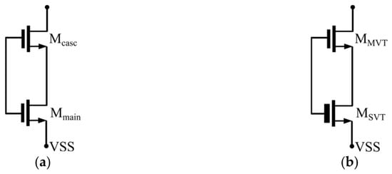
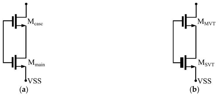
In ULV design, traditional cascoding is often avoided because it requires an additional biasing voltage and increases the minimum output voltage, which limits the signal swing. The self-cascode composite transistor (SCCT) configuration, shown in Figure 1a, provides a compelling solution [17,18,19]. It consists of two transistors (Mcasc and Mmain) of the same type (nMOS or pMOS) connected in series, with their gates tied together.
Figure 1.
(a) N-type self-cascode topology. (b) N-type self-cascode with different threshold transistors: SVT, standard (higher) threshold; MVT, medium (lower) threshold.
The self-biasing effect occurs because the lower transistor (Mmain) is typically designed with a much larger W/L ratio or a longer channel length than the upper transistor (Mcasc). This sizing ensures that both transistors and specifically Mmain remain biased in saturation. In both SI and WI regimes, this composite structure behaves as a single transistor with a significantly higher effective output resistance (rout,eff):
where the bulks of Mmain and Mcasc are assumed to be connected to VSS. This cascode effect multiplies the intrinsic resistance of the main transistor by the product of intrinsic gain and intrinsic resistance of the cascode device, significantly reducing the impact of channel-length modulation. The effective transconductance (gm,eff) of the composite device can be approximated by considering the small-signal current generated by both transistors. However, because they are in series, the same current must flow through both. Analytically, the effective transconductance of the self-cascode is expressed as
Since the denominator approaches unity in saturation, the effective transconductance is almost entirely defined by the transconductance of the Mmain transistor. The total voltage gain (Av) of the self-cascode stage is then the product of its effective transconductance and its effective output resistance:
When both devices operate in the saturation of weak inversion, the high transconductance efficiency (gm/ID) yields a very high Av. This makes the self-cascode an ideal candidate for high-gain, single-stage OTA designs where power consumption and supply voltage are constrained.
3.2. Trade-Offs in W/L Sizing and Threshold Voltage Selection
When sizing the SCCT structure for operation in weak inversion, the design space is defined by a compromise between transconductance efficiency, output impedance, and silicon area.
- W/L Sizing for Efficiency and Area
Case I: Fixed Current (ID,GD = ID,BD): To offset the lower transconductance of the BD-OTA (gmb = η gm), we use a large (W/L)BD. This ensures that the device operates at the absolute peak of the gm/ID curve. While W/L does not increase gm beyond the ID/(nVT) limit, it ensures we do not drop below that limit due to moderate inversion.
Case II: Fixed Transconductance (Gm,GD = Gm,BD): To match GD performance, the BD-OTA requires 1/η more current. Consequently, (W/L)BD is typically scaled up by a factor of 1/η, accepting the trade-off of higher parasitic capacitances.
- 2.
- Output Resistance and Channel Length
To maximize the DC voltage gain, Mcasc can be designed with a longer channel length than Mmain. This minimizes channel-length modulation, increasing rds,casc and boosting the total rout,eff, as derived in (10).
- 3.
- Threshold Voltage
Commercial CMOS processes usually offer standard-, medium- and low-threshold transistors, with decreasing values of the threshold, respectively. As proposed by the authors in [15], using a medium-Vth (MVT) device for Mcasc and a standard-Vth (SVT) device for Mmain, as shown in Figure 1b, we ensure that Mmain remains in the saturation region (VDS ≥ 3VT) even under extremely low supply voltages. This approach decouples the sizing of the cascode from the need to provide high voltage headroom.
- 4.
- Noise
If gm is fixed, the thermal noise power spectral density (4kTγ/gm) remains constant. However, using a large W/L allows us to keep the transistor in weak inversion, where gm is at its maximum possible value for a specific drain current. Furthermore, a large W/L provides a direct benefit in reducing flicker (1/f) noise. By scaling up the width to maintain weak inversion, we inherently increase the total area, which significantly reduces the 1/f noise contribution of the input pair.
In conclusion, for bulk-driven OTAs, where the effective input transconductance is inherently limited by the lower body transconductance (gmb), maximizing the intrinsic gain of the input stage is particularly important. The self-cascode configuration directly addresses this limitation by increasing the effective output resistance of the input branch without requiring additional voltage headroom or extra bias current. Hence, the SC structure allows bulk-driven input stages to recover a significant portion of the gain typically lost compared to gate-driven implementations, while still preserving the ultra-low-voltage capability essential for sub-0.5 V analog design.
4. OTA Topologies
4.1. Gate-Driven OTA
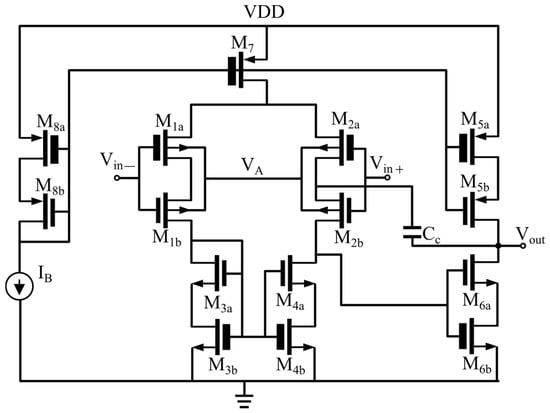
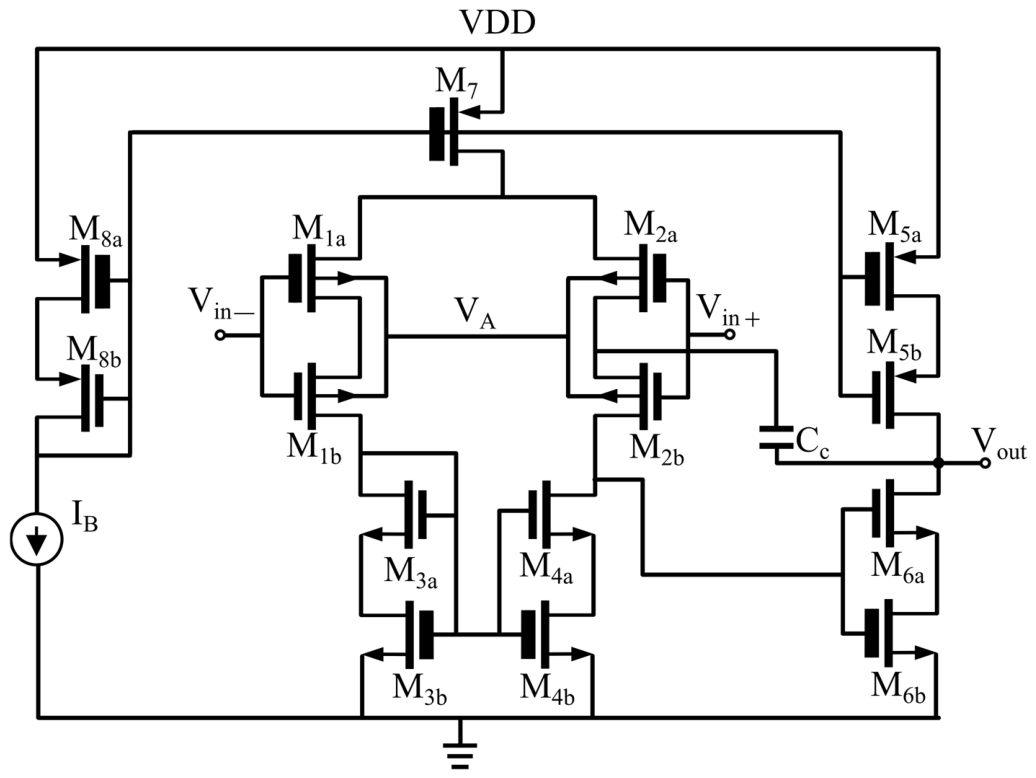
The topology of the gate-driven (GD) OTA, illustrated in Figure 2, represents a complete two-stage OTA. To improve the output resistance and intrinsic gain, all transistors throughout the amplifier consistently utilize the SCCT structure. A regular/thicker gate line drawing style indicates medium/standard threshold voltage transistors. The input stage is configured as a conventional differential pair where the differential input signal (Vin+–Vin−) is applied directly to the gate terminals of the p-channel composite transistors (M1a,b and M2a,b). To achieve similar biasing conditions with the BD counterpart, the bulk of differential stage input transistors in GD is connected to a constant bias voltage, VA.
Figure 2.
SCCT-based gate-driven OTA.
The tail current for this differential pair is established by the p-channel current source M7. The gate of this tail transistor, along with those of the output stage current load (M5a,b), mirrors a weighted copy of the reference current (IB) irrespective of supply voltage fluctuations, which is crucial for maximizing the power-supply rejection ratio (PSRR). The differential pair’s output current is converted from differential to single-ended by the active current mirror load, comprising the n-channel SCCT structures M3a,b and M4a,b. The single-ended output signal from the first stage is then fed to the second gain stage implemented by an n-channel common-source composite transistor M6a,b with M5a,b serving as the load devices.
Regarding voltage levels and regions of operation, the vertical stack of composite transistors combined with the tail transistor (M7) necessitates 5 VDS,SAT (M7, M1a, M1b, M3a and M3b) to maintain subthreshold saturation for all devices, assuming a VDS,SAT of typically 100 mV requires a supply voltage of 500 mV. The use of different threshold flavors helps to balance the threshold requirements of the cascoded stack.
Finally, frequency compensation, essential for stability, is implemented via a current buffer Miller compensation scheme which exploits capacitor CC and the inherent current buffer behavior of transistor M2b [23,24].
4.2. Bulk-Driven OTA
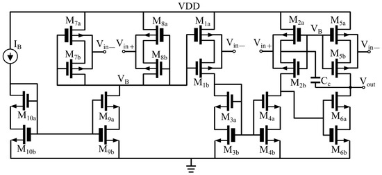
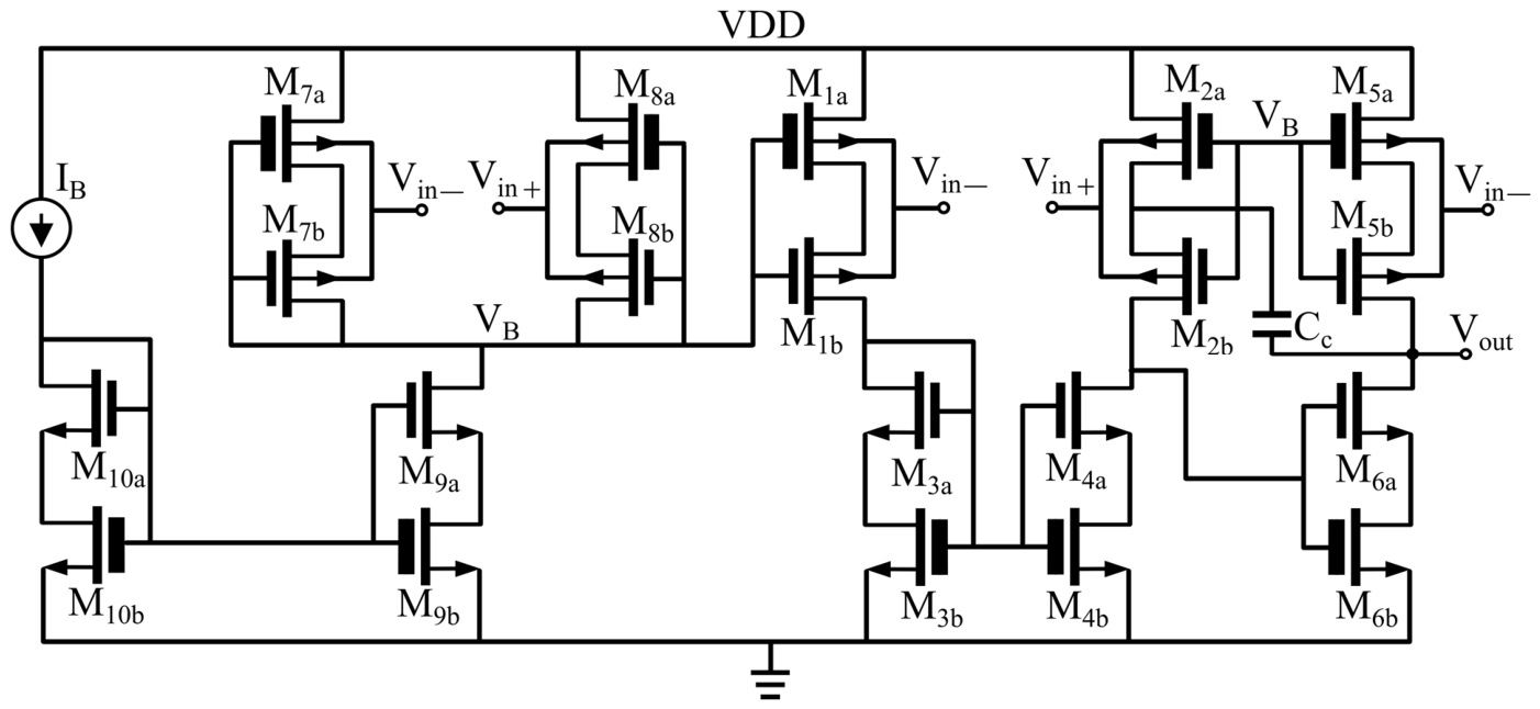
The first stage of the schematic in Figure 3 is composed of a tail-less differential input pair formed by transistors M1a,b and M2a,b. Transistors M3a,b and M4a,b operate as an active load and simultaneously perform the differential-to-single-ended conversion. The second gain stage is realized through a gate-driven common-source configuration using M6a,b, with M5a,b serving as the load devices. The bulk terminal of M5a,b is connected to the inverting input , enabling class AB operation, in which the maximum sourcing and sinking output currents are not limited by the bias current.
Figure 3.
SCCT-based bulk-driven OTA.
The bias current is established by the current source IB together with transistors M7a,b–M10a,b. This network generates the bias voltage VB, which is applied to the gates of both the differential input pair and the output load devices, thereby setting the operating currents in the differential and output branches independently of the supply voltage and the input common-mode level [15,25].
A decrease (increase) in Vin,cm causes VB to increase (decrease), as transistors M7A,B–M8A,B inherently adapt their source-gate voltage to fit their constant bias current. The VB increase (decrease) determines then the bias current of M1A,B–M2A,B constantly and independently of supply and common-mode voltage, resulting in an improved common-mode rejection ratio (CMRR) and power-supply rejection ratio (PSRR).
Note that this common-mode stage feedback arrangement also provides a differential response from the otherwise pseudo-differential pair M1a,b–M2a,b.
Finally, because the architecture stacks up to four transistors vertically (M1a, M1b, M3a and M3b), a voltage headroom of 4VDS,SAT is required. Assuming a typical VDS,SAT of 100 mV, the minimum necessary supply voltage is 400 mV.
5. Comparative Analysis: GD vs. BD OTA Performance
This section provides a detailed comparative analysis of the proposed GD and BD OTA topologies, focusing on key figures of merit including gain, bandwidth, noise, and rejection ratios.
5.1. Differential DC Gain
For a two-stage OTA, the overall differential-mode DC gain (ADM) can be expressed as the product of the individual stage gains:
where Ro1 and Ro2 represent the output resistances of the first and second stages, respectively. These resistances are designed to be approximately equivalent in both GD and BD configurations. Similarly, the second-stage transconductance, Gm2, is approximately identical for both cases and corresponds to the transconductance of the common-source transistor M6b.
The fundamental difference lies in the first-stage transconductance, Gm1. For the GD OTA, Gm1 is the gate transconductance (gm1,2), whereas, for the BD OTA, it is the bulk transconductance (gmb1,2). Since, from (6), gmb = η gm, the intrinsic gain of the BD stage is significantly lower. Consequently,
5.2. Compensation Capacitor and Gain–Bandwidth Product
The Gain–Bandwidth Product (GBW) is the product of the dc gain and the dominant pole frequency. In a two-stage OTA, the dominant pole is established by Miller compensation, where ωp1 = 1/(Ro1Gm2Ro2CC). From (13), the GBW is the ratio of the first-stage transconductance to the compensation capacitance:
The second pole (ωp2), which primarily limits stability and high-frequency performance, is located at the output of the second stage. Its frequency is determined by the transconductance of the second stage (gm2) and the load capacitance (CL). The stability of the amplifier is quantified by the phase margin (ϕm). In a Miller-compensated system, if we neglect the right-half-plane (RHP) zero (often mitigated by a nulling resistor or a current buffer), the phase margin can be expressed as the difference between 180° and the phase shift contributed by the poles at the unity-gain frequency.
Since the dominant pole contributes a 90° phase shift at GBW, the phase margin is determined by the proximity of the second pole:
Substituting the expressions for GBW and ωp2, we obtain
Equation (17) highlights an advantage of bulk-driven architecture. In a BD stage, the transconductance Gm1 = gmb is naturally lower than the gm of a GD stage. To maintain the same phase margin and load capacitance as a GD OTA, the BD design allows for a proportional reduction in the compensation capacitor. Specifically,
Because in (15) both the numerator (Gm1) and the denominator (CC) of the GBW expression scale by the same factor η, the resulting Gain–Bandwidth Product remains theoretically constant between the two architectures, despite the weaker driving capability of the bulk terminal.
5.3. Slew Rate Performance
In two-stage OTA topologies, the slew rate (SR) is governed by two distinct mechanisms related to the charging/discharging of the compensation capacitor and the load capacitor, referred to as the internal and external SR, respectively. For a given bias (tail) current (Ibias), the internal slew rate is defined as
As established in the previous section, BD OTAs require a smaller CC to maintain stability compared to their GD counterparts. Consequently, for the same current budget, BD architectures inherently exhibit a superior internal SR. Furthermore, tail-less BD stages often benefit from intrinsic class AB behavior [26]. These characteristics enhance the transient response, resulting in a more responsive amplifier under large-signal conditions.
5.4. Noise Analysis
The dominant noise contributions in an OTA are primarily localized within the input stage, specifically originating from the input differential pair and the active load current mirrors. In architectures employing self-cascode composite transistors (SCCTs), the noise is predominantly generated by the common-source transistors, while the contribution of the cascode transistors remains negligible. Similarly, the noise from the second stage is attenuated when referred to the input by the high gain of the first stage.
The equivalent input-referred noise power spectral density (PSD), accounting for both thermal (white) and flicker (1/f) components, can be expressed as
In this expression, γ represents the thermal noise coefficient (typically 2/3 for long-channel devices). While advanced sub-micron technologies may require more sophisticated models to account for short-channel effects, (20) serves as a valid basis for a comparative assessment.
The general analytical conclusion is that BD OTAs exhibit higher thermal noise levels due to the inherently lower transconductance (Gm1 = gmb). Furthermore, the term inside the parentheses in (20) cannot be considered negligible in BD OTAs, whereas typically in GD OTAs it is as long as gm3b,4b << gm1a,2a. Finally, flicker noise performance in BD devices is often degraded; the flicker noise coefficient (Kf) can be larger due to the body effect, and the bulk terminal is more susceptible to substrate noise and interface traps, further increasing the 1/f noise floor.
5.5. CMRR and PSRR
The common-mode gain, ACM, is evaluated by applying a common-mode signal vi,CM to the inputs of the two OTAs. The CMRR is obtained as ADM/ACM, where the gain contribution of the second OTA stages does not play any role because it appears on both ADM and ACM.
The CMRR at DC of the GD OTA is expressed as
where rd7 is the output resistance of the tail current generator (M7 in Figure 2) and ε is the M3B–M4B current mirror relative error (i.e., id4/id3 = 1 + ε).
Regarding the PSRR of the GD OTA, it is simulated as an AC signal superimposed on VDD and is treated by the OTA as a common-mode signal. Consequently, it can be demonstrated that the following relation between PSRR (0) and CMRR (0) exists:
Hence, PSRR (0) is almost equal to CMRR (0) in the GD OTA.
For the BD OTA, by inspection of the auxiliary common-mode/biasing section, the voltage vB,CM caused by the common-mode input is
where is the equivalent small-signal resistance offered by transistors M9A,B. This voltage is applied to the gates of transistors M1A-2A, and the resulting small-signal drain current of M2A is therefore
Substituting (23) in (24),
As a result, , where ε’ is the M3B–M4B current mirror relative error. Remembering that , the CMRR at DC is
Comparing (21) and (26), one important distinction lies in the denominator of (26), which contains the subtractive term (gm7A,8A − (gm1A,2A gmb7A,8A/gmb1A,2A)). If the auxiliary transistors (M7–M8) in Figure 3 are perfectly matched and proportionally scaled to the main input transistors (M1–M2) in Figure 3, this term cancels out. In this ideal scenario, the denominator reduces simply to ε’, whereas the numerator is dominated by 2gm7A,8ARoB. Since RoB >> rd7, the massive gain provided in the numerator is more than enough to compensate for the degradation introduced by the transconductance mismatch in the denominator. Therefore, despite the added sensitivity to mismatch between the auxiliary and main pairs, the BD OTA will exhibit a comparable or even greater DC CMRR to the GD OTA.
In a similar manner to (22), the BD OTA exhibits a strong correlation between CMRR (0) and PSRR (0), as any disturbance on the VDD rail is processed by the circuit as a common-mode input.
In summary, the adopted SCCT structure and biasing sub-circuit are expected to yield competitive DC gain, PSRR, and CMRR for the BD OTA.
6. PVT and Corner Simulations
To enable a consistent performance comparison, the circuits shown in Figure 2 and Figure 3 were implemented using the same 180 nm CMOS technology from TSMC. Both designs employ two different “flavors” of transistors. Specifically, medium-threshold and standard-threshold n-channel (p-channel) MOSFETs, with VTH0 values of 310 mV and 500 mV (−240 mV and −490 mV), respectively, were used for the cascode and common-source topologies in the SCCT structures.
The aspect ratios are optimized to achieve subthreshold saturation criteria of |VDS| = 100 mV as summarized in Table 2, together with the bias current of 10 nA and voltage supply (VDD) of 400 mV and 500 mv for BD and GD OTA, respectively.
Table 2.
Transistor aspect ratios and main design settings.
The main small-signal parameters (transconductances and resistances) are summarized in Table 3, and by utilizing these values, the very important comparison parameter η was extracted as and . To achieve a similar PM for fair comparison, the CC required is different, as shown in Table 2. Observe that the CC’s ratio is not exactly η, in order to take into account second order effects (e.g., different output resistance values between GD and BD OTAs and the neglected second poles) and to achieve a similar phase margin in both OTAs.
Table 3.
Small-signal parameters in nominal condition.
In [15], the bulk-driven OTA solution was experimentally validated across all process corners. This was one of the most comprehensive characterizations of BD OTAs in the literature and showed a very good agreement with pre- and post-layout simulations, indicating that the effects of layout parasitics and mismatch were limited for the fabricated BD OTA. Due to the lack of experimental data for the GD counterpart, we base the present comparison on pre-layout simulation results for both designs.
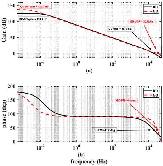
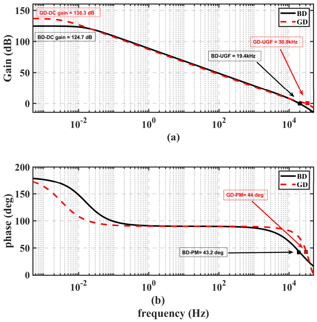
Figure 4 illustrates the frequency response (magnitude and phase) of both the GD and BD designs, showing a DC gain of 136.3 dB and 124.7 dB, respectively. While the GD design exhibits superior gain (+12 dB, compared to the theoretical 20 log(1/η) = 8.4 dB), both architectures achieve, as expected, a comparable Gain–Bandwidth Product (GBW) through a deliberate design trade-off. This results in nearly superimposed roll-off characteristics, as the higher DC gain of the GD design is balanced by the higher dominant pole frequency of the BD design. However, a slight discrepancy is observed in the unity-gain frequency (UGF), with the GD achieving 30.9 kHz compared to 19.35 kHz for the BD. This difference is primarily attributed to the peaking effect near the UGF in the GD response, which extends its crossover point despite the matching of the sub-Hertz slopes. This peaking stems from complex-conjugate poles, as evidenced by the steeper phase variation in the GD above the UGF. Consequently, the GD topology is inherently more challenging to compensate due to the presence of these poles, which are absent in the BD topology. The GBW of both the topologies is well suited for low-frequency application, specifically for biomedical signals, which range from mHz to a maximum of 10 kHz [27]. Therefore, the proposed OTAs provide a sufficient bandwidth margin for biopotential acquisition systems such as ECG, EEG, and EMG front-ends, while maintaining ultra-low-power consumption. Figure 4b illustrates that the phase margin is 43.19° and 44° for BD and GD, respectively. This lower phase margin represents an acceptable trade-off between stability and bandwidth under ULV/ULP regimes. Because of the inherently lower gmb, increasing the PM would require a larger CC, severely penalizing the GBW and slew rate. Finally, as reported in [15], this PM parameter exhibits high stability against PVT variations.
Figure 4.
Frequency response of GD and BD OTAs: (a) magnitude and (b) phase.
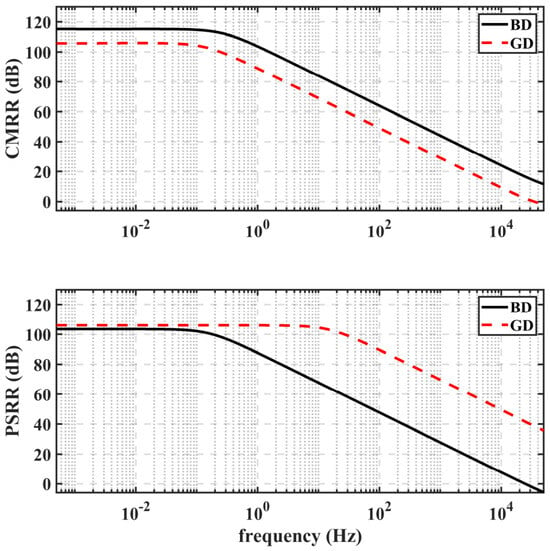
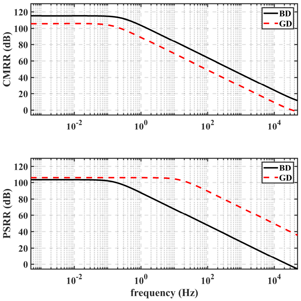
Figure 5 presents the magnitude of CMRR and PSRR versus frequency. The BD design achieves a higher CMRR (0) of 115 dB compared to 106 dB for the GD design, maintaining superior rejection across the entire frequency range. In contrast, the GD design exhibits a marginally higher PSRR (0) of 107 dB over the BD’s 104.5 dB. The primary advantage of the GD architecture, however, lies in its superior frequency response, as it provides a much wider PSRR bandwidth, providing, for example, a rejection level of 50 dB even at frequencies (10 kHz) where the BD response has already significantly deteriorated.
Figure 5.
CMRR and PSRR magnitude versus frequency of GD and BD OTAs.
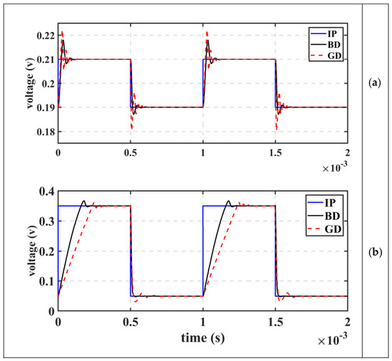
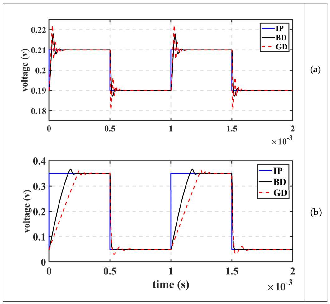
Figure 6a illustrates the small-signal step response for a 20 mV peak-to-peak input. Positive/negative 1% settling time is 95.47/79.83 (µs) for the BD OTA and 112.9/98.37 (µs) for the GD OTA. Figure 6b displays the large-signal step response for a 300 mV peak-to-peak input. Under the same quiescent current, the BD design achieves a significantly higher slew rate, as evidenced by the steeper slope and faster settling time. This enhanced speed is a direct result of the smaller CC required for BD architecture.
Figure 6.
(a) Small-step response and (b) large-step response of GD and BD.
The effect of the intrinsically lower gmb is reflected in the increased flicker and thermal noise for the BD OTA, as seen in Table 4. Interestingly, the ratio between the flicker noise of GD and BD designs (96.4/36.7 = 2.6) is approximately equal to that of the white noise ratio (1.45/0.56 = 2.6) among them. Furthermore, this ratio is approximately equal to 1/η = 2.6.
Table 4.
OTA noise performance comparison.
Table 5 summarizes the performance metrics of both topologies, clearly reflecting the trends discussed in Section 5 under the process corners. The considerably larger intrinsic gate transconductance provides a GD architecture with higher DC gain and lower noise. Also, offset is lower in the GD OTA. Conversely, the lower CC required to achieve the same PM results in better SR and settling time for BD architecture. While PSRR (0) values are similar, the BD architecture shows superior CMRR (0). Nonetheless, both topologies demonstrate robust performance, resulting in low sensitivity in all the process corners.
Table 5.
OTA performance under process corner variation at 27 °C.
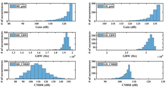
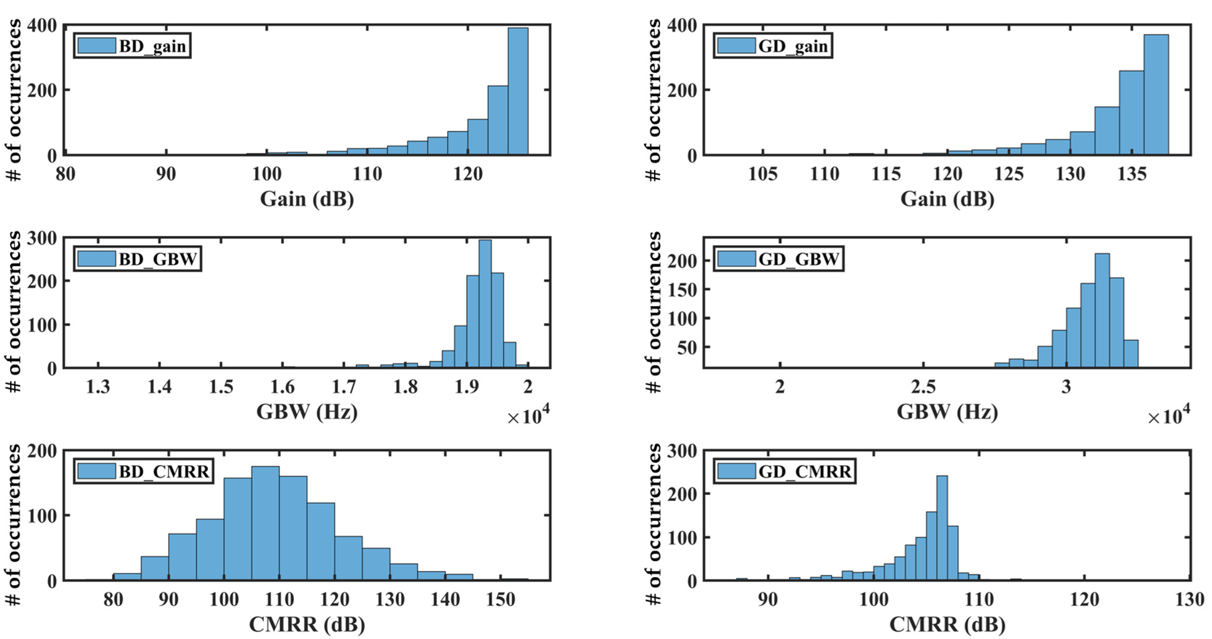
The impact of process mismatches is summarized in Table 6, based on 1000-iteration Monte Carlo simulations. Both architectures exhibit comparable standard deviation values. Meanwhile, Figure 7 illustrates the histogram for gain, GBW and CMRR of both BD and GD topologies, clearly reflecting the results of Table 6.
Table 6.
OTA performance under Monte Carlo simulation results at 27 °C.
Figure 7.
Histogram from 1000 Monte Carlo simulations for gain, GBW and CMRR of BD and GD at 27 °C.
Table 7 illustrates the performance summary of both GD and BD OTAs under temperature variations. It is seen that the GD architecture maintains superior DC gain and GBW across all temperatures, despite a common performance degradation at 80 °C. Conversely, the BD architecture excels in large-signal metrics, delivering faster settling times and higher slew rates. Both designs exhibit stable phase margins, ensuring consistent frequency compensation. Notably, BD architecture demonstrates significantly better CMRR at high temperatures compared to the GD counterpart.
Table 7.
OTA performance under temperature variations and TT corner.
Table 8 illustrates the performance of both the GD and BD OTAs under a supply variation of VDD ± 50 mV. Both designs respond conventionally to supply voltage variations. However, the BD architecture sensitivity is comparably higher than GD due to the reliance of bulk transconductance being strongly affected by bias and substrate conditions.
Table 8.
OTA performance under supply voltage variations and TT corner at 27 °C.
Table 9 shows the performance of both the GD and BD architectures against input common-mode (ICM) voltage variations. The results clearly demonstrate the near-rail-to-rail behavior of the BD architecture. The BD OTA maintains acceptable performance levels even when the input common-mode voltage approaches the positive and lower supply rails, whereas the GD OTA performance deteriorates significantly under the same conditions. Nevertheless, the GD topology still exhibits a wider operating range compared to conventional strong inversion operation.
Table 9.
Performance against input common-mode value TT corner and at 27 °C.
Table 10 presents the state-of-the-art comparison of recently reported ULV/ULP OTAs. The area of the GD circuit presented in this manuscript is estimated based on the implemented BD circuit by considering both the reduction in area due to the smaller number of transistors and the increase in area caused by the larger compensation capacitor. The comparison provides a clear overview of the relative performance of the proposed architectures with respect to existing BD and GD designs. Both OTAs discussed in this manuscript achieve high DC gain, CMRR, and PSRR under ultra-low-voltage operation. Furthermore, among the two proposed architectures, the BD OTA achieves a higher FoML due to its faster slew rate, whereas the GD OTA achieves a higher FoMS owing to its larger GBW.
Table 10.
State-of-the-art ULV/ULP OTAs.
7. Conclusions
This work presented a comprehensive, head-to-head comparison between gate-driven (GD) and bulk-driven (BD) operational transconductance amplifiers operating in the deep-subthreshold, ultra-low-voltage (ULV) and ultra-low-power (ULP) regimes. By leveraging the self-cascode composite transistor (SCCT) structure under identical biasing conditions, a rigorous and fair evaluation framework was established.
This paper addresses common misconceptions surrounding BD designs, offering a more nuanced understanding of the true strengths and limitations of two-stage BD OTAs. Theoretical analysis and extensive simulations demonstrate that, while the inherently higher gate transconductance (gm) of the GD OTA ensures superior small-signal performance, specifically in terms of DC gain, the BD architecture presents notable advantages for ULV analog design. Most prominently, the BD approach enables a true rail-to-rail input common-mode range without the structural complexity of complementary input pairs. Furthermore, the BD OTA excels in large-signal transient metrics; the improved slew rate and faster settling times stem directly from the lower compensation capacitance for the same GBW. Alongside these dynamic benefits, the BD OTA can also achieve comparable CMRR and PSRR performance.
However, the inherently lower bulk transconductance (gmb) makes noise a persistent challenge for BD topologies, resulting in a distinct degradation of both thermal and flicker noise profiles. Ultimately, the analysis confirms that there is no universally optimal architecture. From a practical design perspective, the choice between GD and BD topologies hinges on strict, application-specific design priorities. GD architecture is more suitable for applications requiring higher gain, lower input-referred noise, and wider bandwidth. BD architectures, on the other hand, are preferable for ultra-low-voltage systems demanding rail-to-rail input operation and improved large-signal transient behavior. Therefore, the selection of either topology should primarily depend on the target supply voltage, noise constraints, bandwidth requirements, and input signal range of the intended application.
Author Contributions
Conceptualization: S.P.; data curation: M.O.S. and M.P.; original draft preparation: S.P. and M.O.S.; writing, review and editing: all authors; formal analysis: all authors; supervision: S.P. All authors have read and agreed to the published version of the manuscript.
Funding
This work was developed under project SAMOTHRACE (ECS00000022) and funded by the European Union (NextGeneration EU), through the MUR-PNRR.
Institutional Review Board Statement
Not Applicable.
Informed Consent Statement
Not Applicable.
Data Availability Statement
The original contributions presented in the study are included in the article; further inquiries can be directed to the corresponding author.
Conflicts of Interest
The authors declare no conflicts of interest.
References
- Alioto, M. Enabling the Internet of Things—From Integrated Circuits to Integrated Systems; Springer: Cham, Switzerland, 2017. [Google Scholar]
- Huhta, J.C.; Webster, J.G. 60-hz interference in electrocardiography. IEEE Trans. Biomed. Eng. 1973, BME-20, 91–101. [Google Scholar] [CrossRef] [Scilit]
- Zhang, F.; Holleman, J.; Otis, B.P. Design of Ultra-Low Power Biopotential Amplifiers for Biosignal Acquisition Applications. IEEE Trans. Biomed. Circuits Syst. 2012, 6, 344–355. [Google Scholar] [CrossRef] [Scilit] [PubMed]
- Das, R.; Moradi, F.; Heidari, H. Biointegrated and wirelessly powered implantable brain devices: A review. IEEE Trans. Biomed. Circuits Syst. 2020, 14, 343–358. [Google Scholar] [CrossRef] [Scilit] [PubMed]
- Jeon, H.; Kim, Y.-B.; Choi, M. Standby Leakage Power Reduction Technique for Nanoscale CMOS VLSI Systems. IEEE Trans. Instrum. Meas. 2010, 59, 1127–1133. [Google Scholar] [CrossRef] [Scilit]
- Monsurró, P.; Pennisi, S.; Scotti, G.; Trifiletti, A. Exploiting the Body of MOS Devices for High Performance Analog Design. IEEE Circuits Syst. Mag. 2011, 11, 8–23. [Google Scholar] [CrossRef] [Scilit]
- Venezia, C.; Ballo, A.; Grasso, A.D.; Rizzo, A.; Ribellino, C.; Pennisi, S. 46-nA high-PSR CMOS buffered voltage reference with 1.2–5 V and –40 °C to 125 °C operating range. IEEE Trans. Very Large Scale Integr. (VLSI) Syst. 2025, 33, 326–336. [Google Scholar] [CrossRef] [Scilit]
- Huijsing, J.H.; Linebarger, D. Low-voltage operational amplifier with rail-to-rail input and output ranges. IEEE J. Solid-State Circuits 1985, 20, 1144–1150. [Google Scholar] [CrossRef] [Scilit]
- Silveira, F.; Flandre, D.; Jespers, P.G. A g/sub m//I/sub D/based methodology for the design of CMOS analog circuits and its application to the synthesis of a low-power OTA. IEEE J. Solid-State Circuits 1996, 31, 1314–1319. [Google Scholar] [CrossRef] [Scilit]
- Hogervorst, R.; Tero, J.P.; Eschauzier, R.G.; Huijsing, J.H. A compact power-efficient 3 V CMOS rail-to-rail input/output operational amplifier. IEEE J. Solid-State Circuits 1994, 29, 1505–1513. [Google Scholar] [CrossRef] [Scilit]
- Ballo, A.; Grasso, A.D.; Pennisi, S.; Susinni, G. A 0.3-V 8.5-μA Bulk-Driven OTA. IEEE Trans. Very Large Scale Integr. (VLSI) Syst. 2023, 31, 1444–1448. [Google Scholar] [CrossRef] [Scilit]
- Moghaddam, A.K.; Chuah, J.H.; Ramiah, H.; Ahmadian, J.; Mak, P.-I.; Martins, R.P. A 73.9–efficiency CMOS rectifier using a lower DC feeding (LDCF) self-body-biasing technique for far-field RF energy harvesting systems. IEEE Trans. Circuits Syst. I Reg. Pap. 2017, 64, 992–1002. [Google Scholar] [CrossRef] [Scilit]
- Ballo, A.; Carvajal, R.G.; Grasso, A.D.; Luján-Martínez, C.I.; Pennisi, S.; Venezia, C. 0.35-V SR-enhanced bulk-driven OTA for loads up to 10 nF. IEEE Trans. Circuits Syst. I Reg. Pap. 2024, 71, 6410–6418. [Google Scholar] [CrossRef] [Scilit]
- Blalock, B.J.; Allen, P.E. A low-voltage bulk-driven MOSFET current mirror for CMOS technology. In Proceedings of the IEEE International Symposium on Circuits and Systems (ISCAS 1995), Seattle, WA, USA, 30 April–3 May 1995; Volume 3, pp. 1972–1975. [Google Scholar]
- Shah, M.O.; Privitera, M.; Ballo, A.; Alioto, M.; Pennisi, S. 0.4-V nW-Power High-Gain Bulk-Driven Two-Stage OTA With Self-Cascode Composite Transistors and Intrinsic Current-Buffer Miller Compensation. IEEE Trans. Circuits Syst. I Reg. Pap. 2025, 72, 7553–7564. [Google Scholar] [CrossRef] [Scilit]
- Pennisi, S.; Privitera, M.; Shah, M.O. Comparitive Analysis of Bulk-Driven and Gate-Driven Self-Cascode OTA in Subthreshold MOS. In Proceedings of the 2025 32nd IEEE International Conference on Electronics, Circuits and Systems (ICECS), Marrakech, Morocco, 17–19 November 2025; pp. 1–4. [Google Scholar]
- Galup-Montoro, C.; Schneider, M.C.; Loss, I.J.B. Series-parallel association of FET’s for high gain and high frequency applications. IEEE J. Solid-State Circuits 1994, 29, 1094–1101. [Google Scholar] [CrossRef] [Scilit]
- Xu, D.; Liu, L.; Xu, S. High DC gain self-cascode structure of OTA design with bandwidth enhancement. Electron. Lett. 2016, 52, 740–742. [Google Scholar] [CrossRef] [Scilit]
- de Souza, M.; Pavanello, M.A.; Flandre, D. Analog performance of asymmetric self-cascode p-channel fully depleted SOI transistors. In Proceedings of the 8th International Caribbean Conference on Devices, Circuits and Systems (ICCDCS), Playa del Carmen, Mexico, 14–17 March 2012; pp. 1–4. [Google Scholar]
- Enz, C.C.; Vittoz, E.A. (Eds.) Tradeoffs and Optimization in Analog CMOS Design; John Wiley & Sons, Ltd.: Chichester, UK, 2008; pp. 295–374. [Google Scholar]
- Alioto, M. Ultra-low power VLSI circuit design demystified and explained: A tutorial. IEEE Trans. Circuits Syst. I Reg. Pap. 2012, 59, 3–29. [Google Scholar] [CrossRef] [Scilit]
- Alioto, M. Understanding DC behavior of subthreshold CMOS logic through closed-form analysis. IEEE Trans. Circuits Syst. I Reg. Pap. 2010, 57, 1597–1607. [Google Scholar] [CrossRef] [Scilit]
- Palmisano, G.; Palumbo, G. A compensation strategy for two-stage CMOS opamps based on current buffer. IEEE Trans. Circuits Syst. I Fundam. Theory Appl. 1997, 44, 257–262. [Google Scholar] [CrossRef] [Scilit]
- Aloisi, W.; Palumbo, G.; Pennisi, S. Design methodology of Miller frequency compensation with current buffer/amplifier. IET Circuits Devices Syst. 2008, 2, 227–233. [Google Scholar] [CrossRef] [Scilit]
- Grech, I.; Micallef, J.; Azzopardi, G.; Debono, C.J. A low voltage Wide-Input-Range bulk-input CMOS OTA. Anal. Integr. Circuits Signal Process. 2005, 43, 127–136. [Google Scholar] [CrossRef] [Scilit]
- Shah, M.O.; Ballo, A.; Pennisi, S. Bulk-Driven CMOS Differential Stages for Ultra-Low-Voltage Ultra-Low-Power Operational Transconductance Amplifiers: A Comparative Analysis. Electronics 2025, 14, 2085. [Google Scholar] [CrossRef] [Scilit]
- Martinek, R.; Ladrova, M.; Sidikova, M.; Jaros, R.; Behbehani, K.; Kahankova, R.; Kawala-Sterniuk, A. Advanced Bioelectrical Signal Processing Methods: Past, Present and Future Approach—Part I: Cardiac Signals. Sensors 2021, 21, 5186. [Google Scholar] [CrossRef] [Scilit]
- Della Sala, R.; Nicolini, G.; Trifiletti, A.; Scotti, G. A 0.4V 1.9-nW Bulk-Driven Cascode OTA Achieving 75-dB DC Gain With Replica-Bias Assisted PVT Robustness. IEEE Trans. Circuits Syst. I Regul. Pap. 2026. early access. [Google Scholar] [CrossRef] [Scilit]
- Akbari, M.; Hussein, S.M.; Hashim, Y.; Tang, K.-T. 0.4-V Tail-Less Quasi-Two-Stage OTA Using a Novel Self-Biasing Transconductance Cell. IEEE Trans. Circuits Syst. I Regul. Pap. 2022, 69, 2805–2818. [Google Scholar] [CrossRef] [Scilit]
- Khateb, F.; Kulej, T.; Akbari, M.; Tang, K.-T. A 0.5-V Multiple-Input Bulk-Driven OTA in 0.18-μm CMOS. IEEE Trans. Very Large Scale Integr. (VLSI) Syst. 2022, 30, 1739–1747. [Google Scholar] [CrossRef] [Scilit]
- Khateb, F.; Kulej, T.; Akbari, M.; Kumngern, M. 0.5-V High Linear and Wide Tunable OTA for Biomedical Applications. IEEE Access 2021, 9, 103784–103794. [Google Scholar] [CrossRef] [Scilit]
- Radman, M.; Sodagar, A.M. A 35.2-kHz, 75.4-dB Bulk-Driven OTA Using Degenerative Current Tram Structure. IEEE Trans. Very Large Scale Integr. (VLSI) Syst. 2025, 33, 3228–3238. [Google Scholar] [CrossRef] [Scilit]
- Sala, R.D.; Centurelli, F.; Monsurrò, P.; Scotti, G.; Trifiletti, A. A 0.3V Rail-to-Rail Three-Stage OTA With High DC Gain and Improved Robustness to PVT Variations. IEEE Access 2023, 11, 19635–19644. [Google Scholar] [CrossRef] [Scilit]
- Qin, Z.; Tanaka, A.; Takaya, N.; Yoshizawa, H. 0.5-V 70-nW rail-to-rail operational amplifier using a cross-coupled output stage. IEEE Trans. Circuits Syst. II Exp. Briefs 2016, 63, 1009–1013. [Google Scholar] [CrossRef] [Scilit]

Disclaimer/Publisher’s Note: The statements, opinions and data contained in all publications are solely those of the individual author(s) and contributor(s) and not of MDPI and/or the editor(s). MDPI and/or the editor(s) disclaim responsibility for any injury to people or property resulting from any ideas, methods, instructions or products referred to in the content. |
© 2026 by the authors. Licensee MDPI, Basel, Switzerland. This article is an open access article distributed under the terms and conditions of the Creative Commons Attribution (CC BY) license.