


Abstract
Distribution networks face low supply reliability and limited fault-recovery capability. Flexible interconnection devices enable looped operation of AC feeders and facilitate optimal power-flow control, which helps address these operational challenges. This paper proposes a novel medium-voltage flexible interconnection device with a star-connected topology, together with a compact power-module structure and its main-circuit topology. Because distribution networks often contain high background harmonics, a control scheme is developed for the device, comprising a phase-locked loop, hierarchical capacitor-voltage control, and an inner current-control loop. A harmonic-current compensation control strategy is further designed to suppress current harmonics. A hardware-in-the-loop (HIL) testing platform is built to validate the proposed strategy. The results show that the proposed topology enables flexible interconnection of distribution networks, and the proposed control strategy operates stably under high background harmonics while effectively compensating current harmonics.
1. Introduction
The traditional operational paradigm of distribution networks—“closed-loop design and open-loop operation”—has led to several challenges, including limited power supply reliability and limited fault-recovery capability [1]. In addition, this operational mode results in low utilization of grid resources, limited renewable energy hosting capability, and high costs for grid upgrading and reconstruction [2]. Such a contradictory operating mechanism has created a vicious cycle of high-redundancy design and low-efficiency operation, accompanied by strong security constraints yet weak regulation capability. Flexible interconnection devices can enable looped operation of AC feeders, optimize power-flow control, and rapidly transfer loads during faults, thereby improving power supply reliability. Consequently, they have become a key technological solution for addressing the operational challenges of distribution networks [3].
At present, extensive studies have been conducted on the topology and control strategies of flexible interconnection devices. Most existing research adopts the back-to-back topology based on the Modular Multilevel Converter (MMC) [4], while some studies further improve this structure. For example, Ref. [5] proposes a dual active full-bridge converter topology with input-series and output-series configuration. Ref. [6] presents a general high-frequency-link analysis and an associated optimization method for dual active bridge converters, which can guide the design of the isolated DC–DC stage in flexible interconnection devices. Ref. [7] employs a cascaded power electronic transformer combined with cascaded H-bridges, enabling flexible interconnection between a DC port and multiple AC ports, while an intermediate-frequency resonant module is utilized to achieve resonant control and reduce converter volume and cost. Most of these topologies are optimized based on the MMC structure used in flexible DC transmission systems. However, they do not fully consider the characteristics of medium-voltage flexible interconnection devices, which typically do not require long-distance DC power transmission and therefore do not need a high DC bus voltage. Considering this feature, the conventional double-star configuration can be optimized into a single-star or delta configuration, eliminating the high-voltage DC bus to reduce the number of power modules and lower equipment cost.
Regarding control strategies, most device-level control schemes focus on power flow control and operational stability. For instance, Ref. [8] proposes a mixed-frequency modulation strategy, in which the power-frequency control regulates power flow through a single current loop, while the intermediate-frequency control stabilizes capacitor voltage through a dual closed-loop voltage–current control. Ref. [9] presents an improved control strategy with voltage feedforward compensation for flexible interconnection devices to enhance disturbance rejection capability. Ref. [10] employs multi-objective optimization to determine the parameters of the current-loop controller, thereby improving dynamic response characteristics. However, as a four-quadrant fully controllable power electronic device, a flexible interconnection device inherently possesses strong capability for harmonic mitigation, yet research in this aspect remains relatively limited.
To address these issues, this paper proposes a novel star-connected topology for a medium-voltage flexible interconnection device. The proposed topology features a reduced number of power modules, intermediate-frequency isolation, and no requirement for inter-phase circulating current control, enabling a lightweight design that is suitable for outdoor installation while reducing construction cost. These advantages enhance the practical applicability and replicability of flexible interconnection devices. Based on the proposed topology, a control strategy with harmonic compensation capability is developed, which not only fulfills the basic control requirements of the device but also improves the power quality of the distribution network. Finally, an HIL testing platform based on a Real-Time Digital Simulator (RTDS) is established to verify the effectiveness of the proposed control strategy.
2. Star-Connected Flexible Interconnection Device Topology
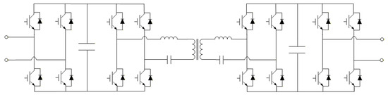
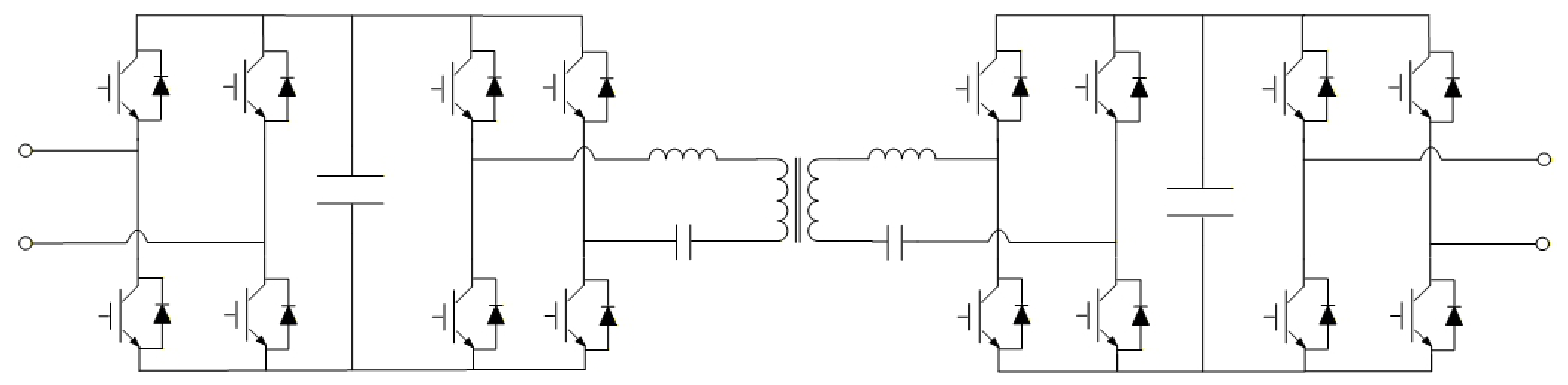
The star-connected flexible interconnection device is composed of three converter arms interconnected in a star configuration. A compact power module structure, as shown in Figure 1, is designed to achieve high power density for the device. The power module adopts a three-stage architecture, enabling bidirectional energy flow.
Figure 1.
Topology of the compact power module.
The intermediate isolation stage is implemented using a bidirectional DC/DC converter, which adopts a dual-active-bridge (DAB) topology. The high-frequency isolation transformer integrates two resonant inductors of a bidirectional LLC resonant circuit. On both sides of the converter, H-bridge structures are employed to interface with the AC stages.
Different types of flexible interconnection devices can be formed by adopting different connection methods for the power modules on both sides. When one side adopts a parallel connection and the other side adopts a series connection, the series side can be connected to the medium-voltage distribution network, while the parallel side is connected to the low-voltage distribution network, thereby enabling flexible interconnection between medium-voltage and low-voltage distribution networks and providing voltage transformation capability.
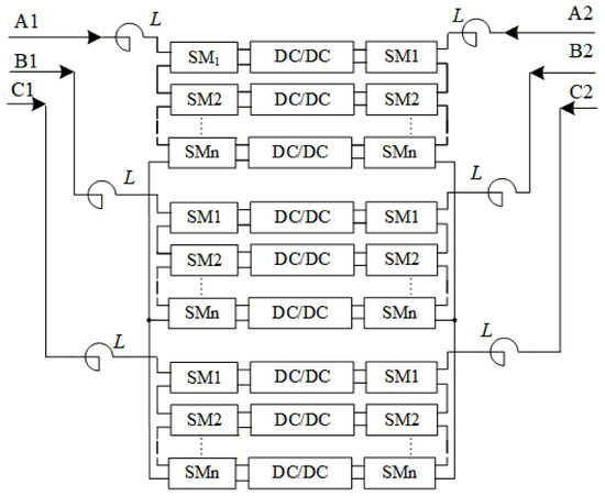
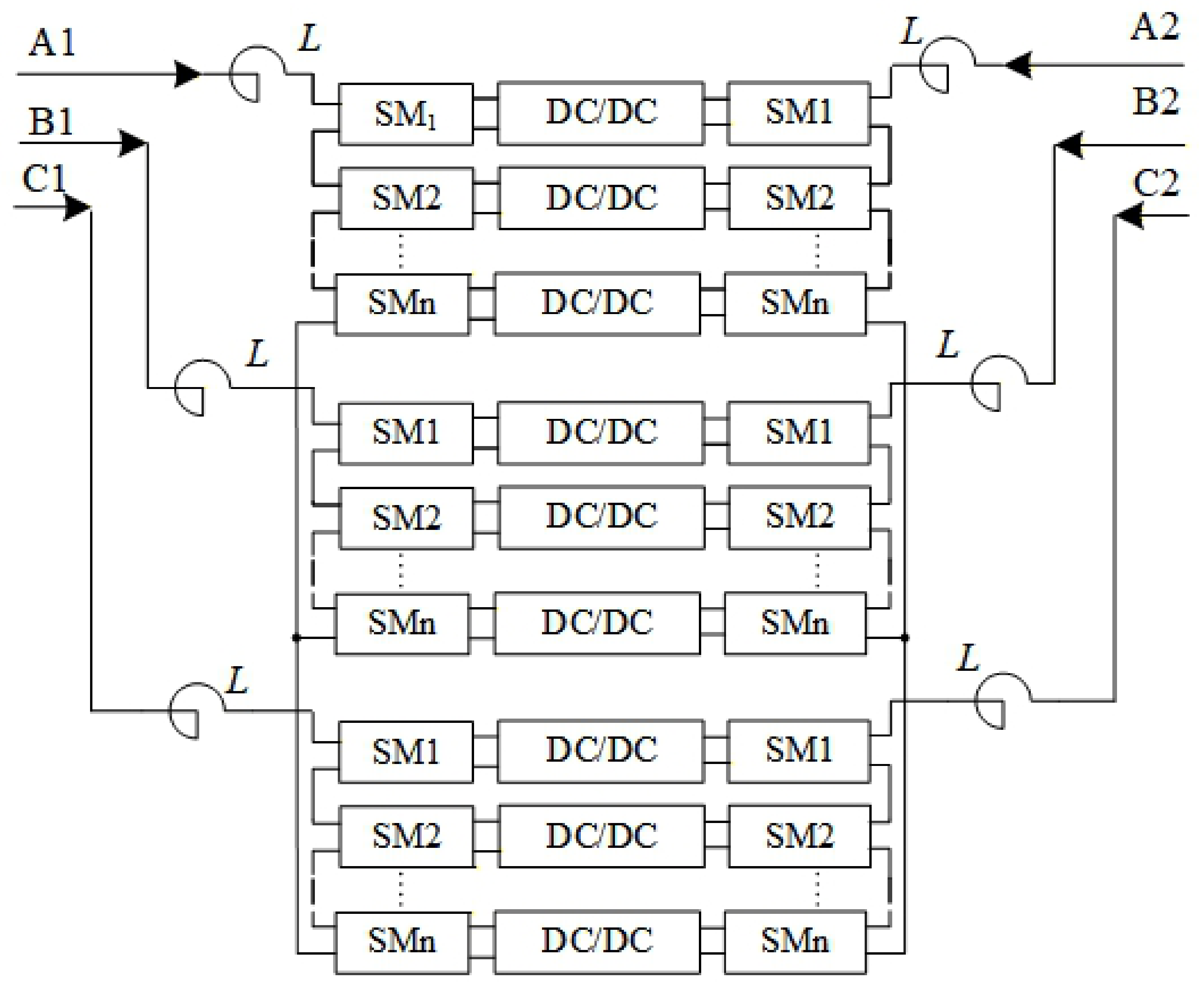
As shown in Figure 2, when both sides adopt a series connection, flexible interconnection can be realized between medium-voltage distribution networks with the same voltage level.
Figure 2.
Main circuit topology of the medium-voltage interconnection device.
3. Control Strategy Under High Background Harmonics
The harmonic compensation capability of a flexible interconnection device becomes practically valuable only when it is connected to a system with significant background harmonics. Therefore, when investigating the harmonic compensation control function of the device, it is necessary to study the steady-state control strategy under high background harmonic conditions.
Considering scenarios in which the connected system contains high levels of voltage and current harmonics, control strategies suitable for such conditions are designed. These include a PLL, an inner current control loop, and a capacitor-voltage balancing strategy, all of which are robust against high background harmonics. The objective is to ensure that the flexible interconnection device can operate stably and reliably even under high background harmonic environments.
3.1. Phase-Locked Loop Design
When grid voltage contains harmonic components, the harmonics appear as AC components in the fundamental rotating reference frame, which may enter the control loop and adversely affect device operation. Therefore, it is necessary to mitigate the influence of grid voltage harmonics on the PLL.
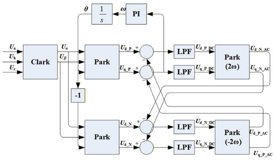
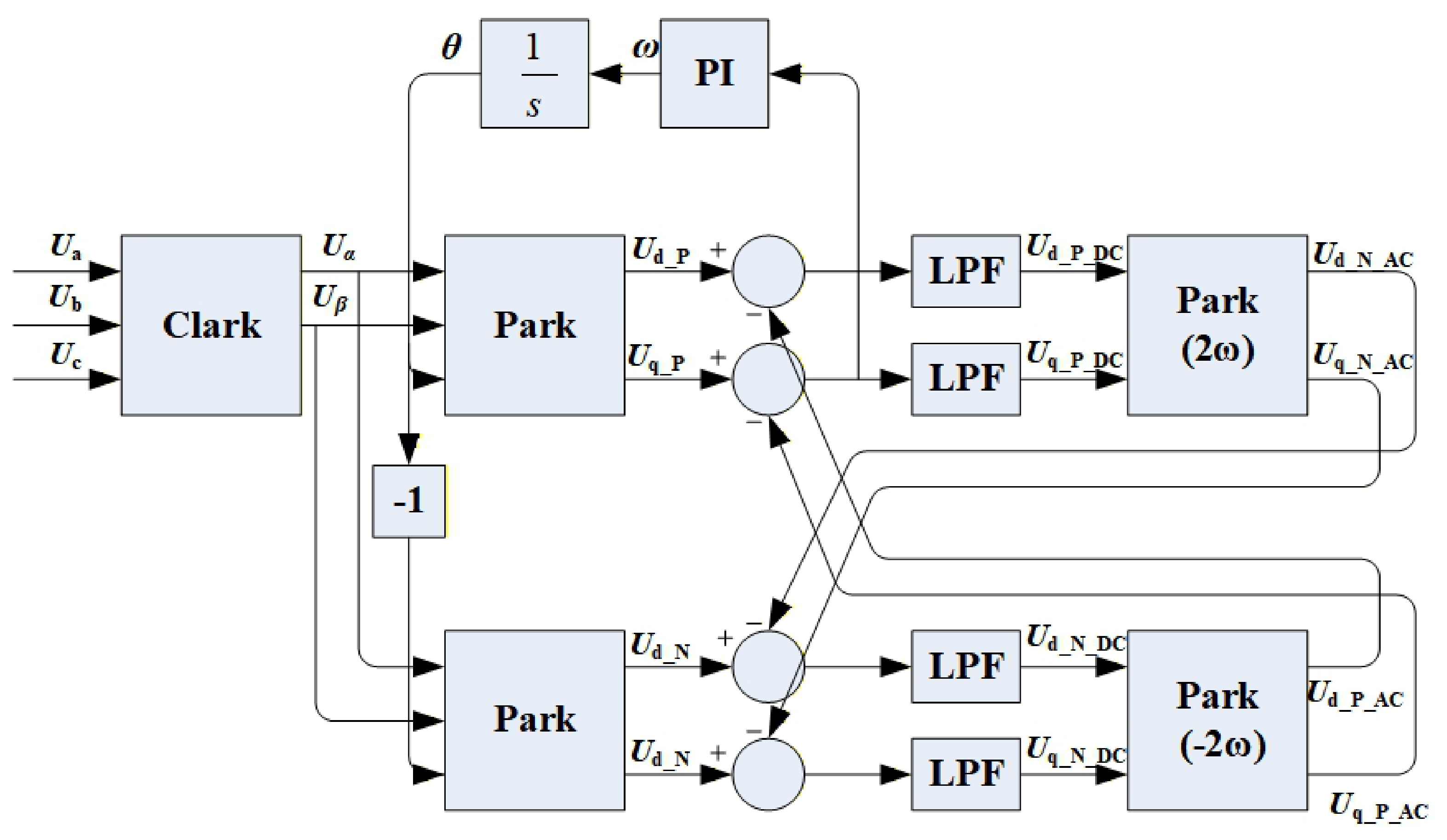
The dual synchronous rotating reference frame PLL (DSRF-PLL) can effectively reduce the influence of the negative-sequence voltage component [11]. Its structure is shown in Figure 3. When the phase angle is small, the approximation holds. The transfer function of the PI controller is , and the transfer function of the low-pass filter (LPF) is . When the input is the phase error and the output is the estimated angular frequency , the open-loop transfer function of the PLL can be expressed as:
where U represents the amplitude of the voltage input to the PLL.
Figure 3.
Structure of the dual synchronous rotating coordinate transformation phase-locked loop.
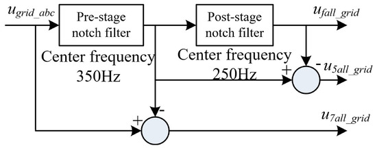
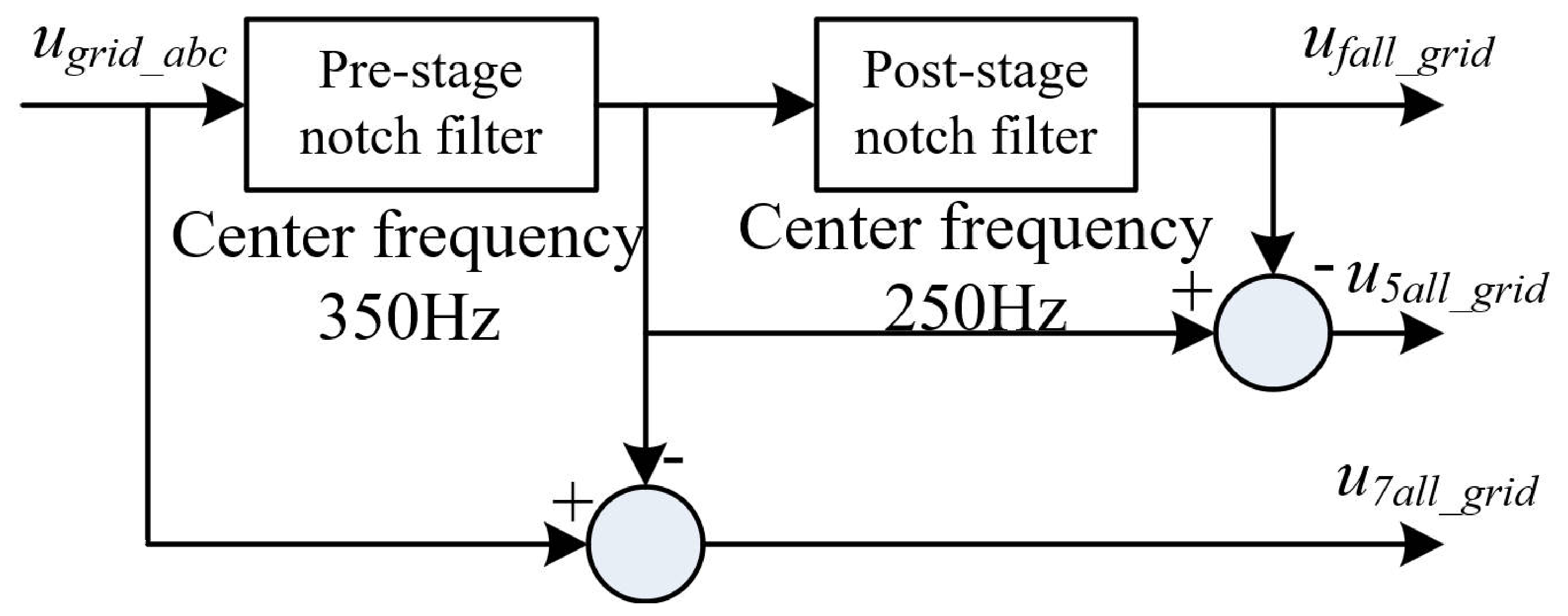
The above PLL has a certain capability to suppress low-order harmonics, and when the harmonic content of the grid voltage is relatively small, it can accurately obtain the phase of the fundamental grid voltage. However, when the harmonic content of the grid voltage becomes significant, the estimated voltage amplitude obtained by the PLL may contain AC ripple components. To address this issue, a two-stage notch filter is designed, as shown in Figure 4, to eliminate harmonic components and extract the fundamental voltage component. Compared with the conventional low-pass filtering approach, this method improves the response speed and reduces phase shift.
Figure 4.
Extraction of the fundamental component of voltage.
A notch filter is a special case of a band-stop filter, whose stopband is narrower than that of a conventional band-stop filter. Its transfer function can be expressed as:
where A is the passband gain, Q is the quality factor, and is the center angular frequency. The parameter A denotes the passband gain of a single notch filter. The two-stage notch filter mentioned above (see Figure 4) is realized by cascading two such notch filters in series, so that its overall transfer function is the product of the two individual transfer functions of Equation (2).
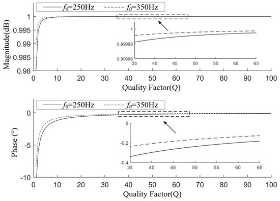
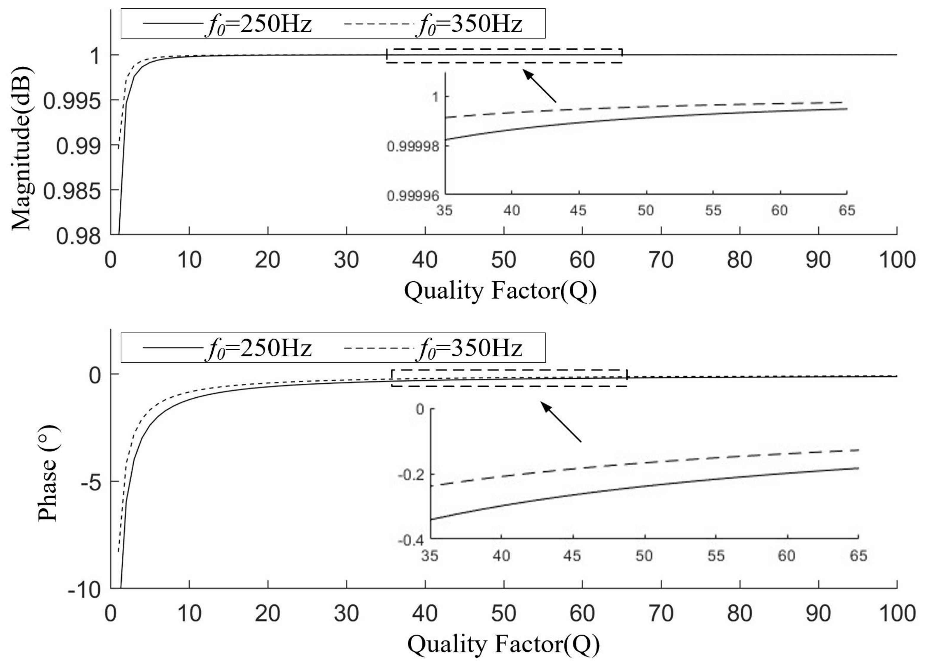
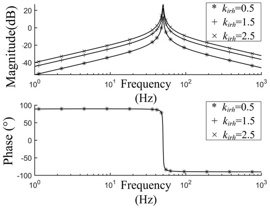
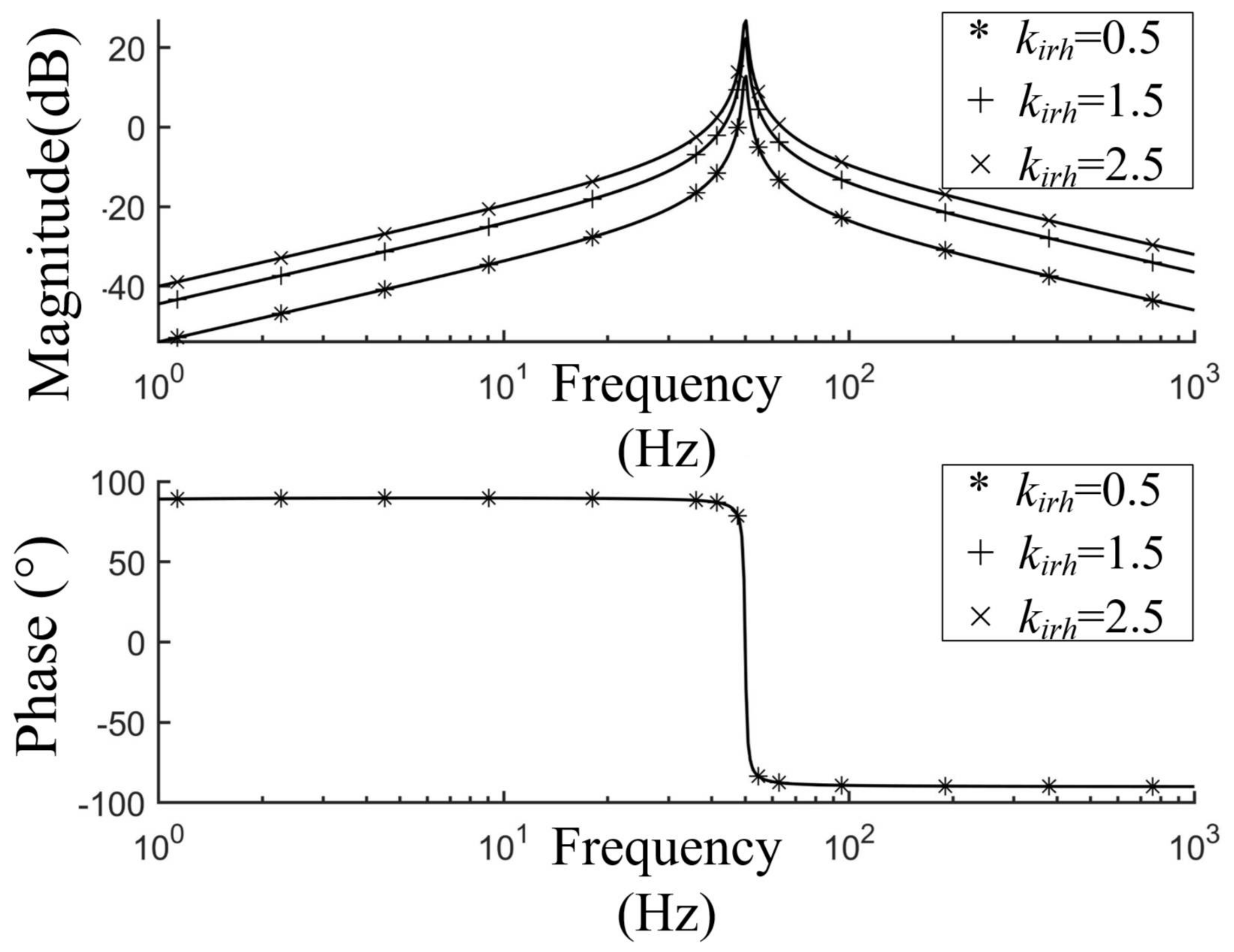
The relationship between the quality factor and the amplitude and phase characteristics when equals 250 Hz and 350 Hz is shown in Figure 5. It can be observed that when is 250 Hz or 350 Hz, a larger Q results in a smaller influence of the notch filter on the amplitude and phase of the fundamental component. When , for Hz the amplitude is ( dB) and the phase delay is ; for Hz the amplitude is ( dB) and the phase delay is . Therefore, when , the phase delay of the notch filters at both 250 Hz and 350 Hz is less than .
Figure 5.
Relationship between the quality factor and the amplitude and phase.
Accordingly, two notch filters are designed with passband gain , center angular frequencies and , and quality factor .
3.2. DC Voltage Control
To ensure stable operation of the flexible interconnection device under high background harmonic conditions, a three-layer DC bus voltage balancing control strategy for the power modules is designed. The first layer is the overall DC bus voltage control, which regulates the total active power input to the device by controlling the positive-sequence d-axis current. The second layer is the inter-converter-arm voltage balancing control, which regulates the active power of the three converter arms by controlling the negative-sequence dq-axis current. The third layer is the intra-arm voltage balancing control, which balances the distribution of active power within each arm by adjusting the output voltage of individual power modules.
Overall Voltage Control Strategy. Based on the principle of power balance, the relationship among the DC voltage, DC current, and AC current in the dq rotating coordinate system can be expressed as:
where is the equivalent capacitance on the DC side, is the DC bus voltage, is the DC current, is the load current, N is the number of inserted power modules, is the voltage of a single power module, and and are the dq components of the AC-side voltage. Similarly, and represent the dq components of the AC-side current.
By performing small-signal linearization around the DC operating point of the average model in the dq frame, the small-signal mathematical model can be obtained as
The DC voltage PI controller is designed as:
where is the average value of the module voltage, is the reference voltage of the module, and and are the proportional and integral gains of the DC voltage PI controller.
Inter-Converter-Arm Voltage Balancing Strategy. The average active power of each converter arm within one fundamental-frequency cycle is given by Equation (6). As indicated in Equation (6), the active power of the three converter arms consists of four components. Among them, the four components generated by , , , and are denoted as , , , and , respectively. In particular, the negative-sequence component , which is generated by the interaction between the negative-sequence voltage and the positive-sequence current, differs among the three converter arms. If the device does not inject negative-sequence current, the unequal will lead to an imbalance of the DC-link voltages among the converter arms.
After negative-sequence current is injected, the interaction between the positive-sequence voltage and the negative-sequence current produces an additional active power component , which modifies the active power distribution among the three converter arms. By regulating the amplitude and phase of the negative-sequence current, the active power among the converter arms can be balanced.
In Equation (6), , , and represent the active powers of phases A, B, and C, respectively; and denote the positive-sequence and negative-sequence voltages, and denote the positive-sequence and negative-sequence currents, and , , and are the phase angles of the positive-sequence voltage, the negative-sequence current, and the negative-sequence voltage, respectively.
Therefore, the essence of the negative-sequence current injection method is to regulate the phase angles of the currents in the three converter arms by injecting negative-sequence current, such that the arm currents are orthogonal to the voltages across the converter arms. As a result, the active power flowing into each converter arm becomes zero, thereby achieving DC voltage balancing among the converter arms.
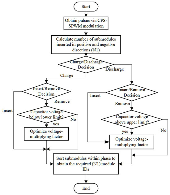
Voltage Balancing Control Strategy for the Converter Arm. The number of cascaded power modules in the converter arm of a flexible interconnection device is relatively small. Therefore, the carrier phase-shifted sinusoidal pulse width modulation (CPS-SPWM) technique is generally adopted to improve power quality [12]. However, when the grid voltage contains significant harmonic components, this method exhibits relatively weak disturbance rejection capability and limited voltage balancing performance among the power modules within the same phase, which may lead to power-module overvoltage problems [13]. To address this issue, a hybrid modulation strategy is proposed in this paper. Based on the conventional CPS-SPWM strategy, an intra-phase power-module sorting-based voltage balancing strategy is introduced. This approach not only mitigates the harmonic problems of the nearest-level-modulation strategy when the number of power modules is small, but also enhances the anti-disturbance capability of intra-phase power-module voltage balancing.
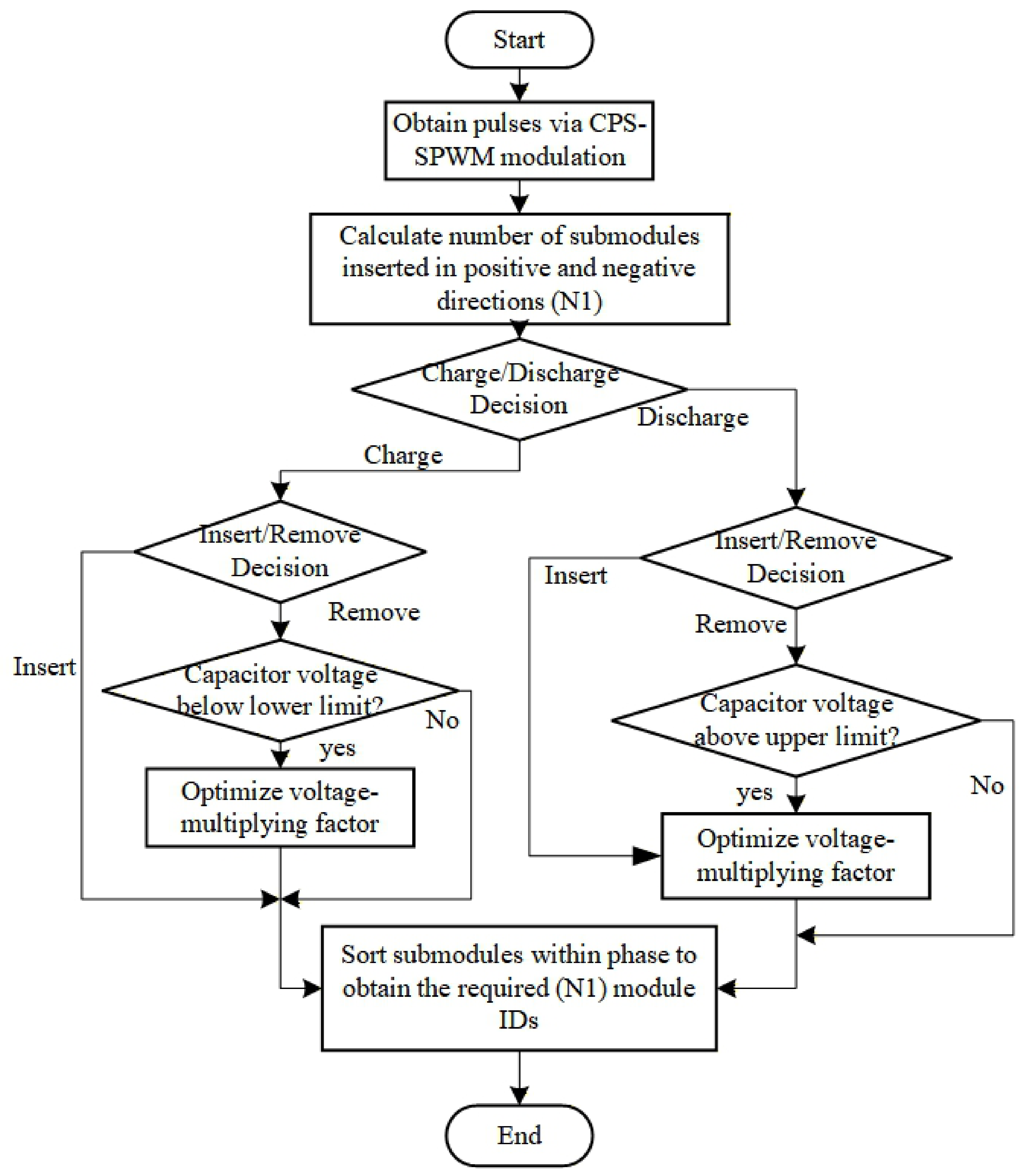
The proposed hybrid modulation strategy is illustrated in Figure 6, and the implementation procedure is summarized as follows:
Figure 6.
Flowchart of the hybrid modulation strategy.
- The switching pulses are generated based on the conventional CPS-SPWM strategy.
- According to the switching pulses, the number of power modules operating in the positive or negative insertion state is determined and denoted as .
- Based on the required number of inserted power modules , the nearest level modulation strategy is implemented.
Meanwhile, to realize the output of cascaded voltage levels obtained from CPS-SPWM through nearest level modulation, a relatively short nearest-level-modulation (NLM) control period is adopted. This accelerates the sorting-based voltage balancing process and reduces the harmonics introduced by the modulation to a level comparable to that of CPS-SPWM.
3.3. Inner-Loop Current Control Strategy
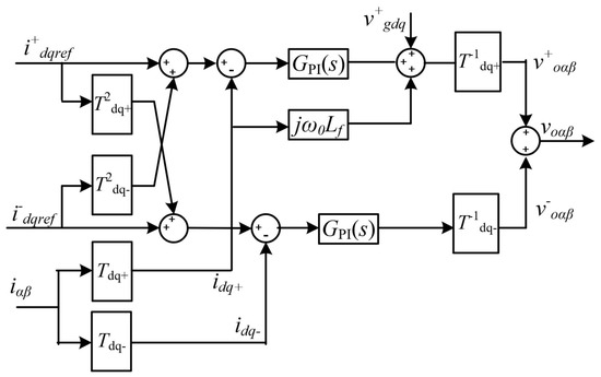
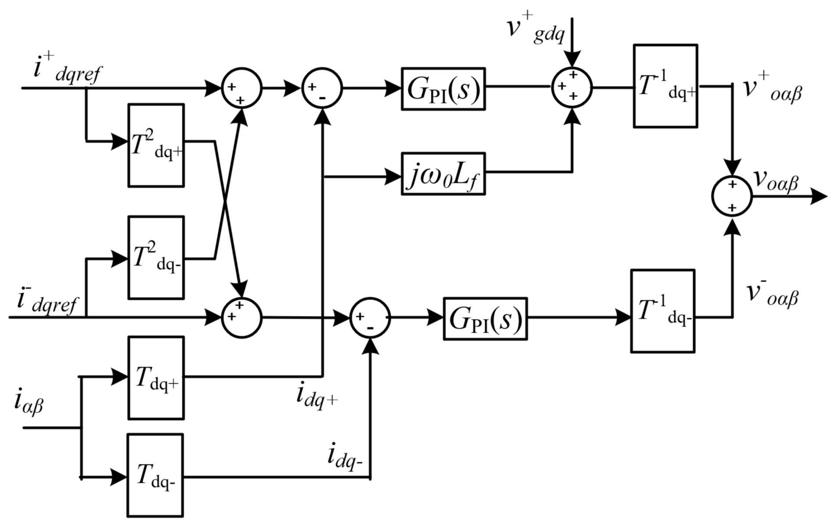
To achieve DC voltage balancing among converter arms using the negative-sequence current injection method, the flexible interconnection device adopts a dual-sequence current control scheme based on the conventional double closed-loop control structure. Specifically, the positive- and negative-sequence components of the inner-loop current are simultaneously regulated. An unbalanced PLL is employed to separate the positive- and negative-sequence components of the device current, and the negative-sequence current is incorporated into the control loop. The detailed control strategy is illustrated in Figure 7. In this approach, both positive- and negative-sequence currents are regulated in their respective synchronous reference frames. In the positive-sequence reference frame, the positive-sequence DC current and the negative-sequence 100 Hz current component are controlled. In the negative-sequence reference frame, the positive-sequence 100 Hz current component and the negative-sequence DC current are regulated.
Figure 7.
Block diagram of the current inner loop with negative-sequence current control.
By introducing a cross-coupled current reference transfer link, the explicit decomposition process of positive- and negative-sequence current components can be avoided. Owing to this cross-coupling mechanism, both positive- and negative-sequence currents are simultaneously regulated by the PI controllers in the positive-sequence dq frame and the negative-sequence dq frame. Under normal grid voltage conditions, only the positive-sequence current reference exists in the command signal. The PI controller in the positive-sequence dq frame and the proportional controller in the negative-sequence dq frame jointly regulate the actual current to track the reference without steady-state error. When the grid voltage becomes unbalanced, the current reference contains both positive- and negative-sequence components. In this case, the proportional controllers in both the positive-sequence dq frame and the negative-sequence dq frame enable rapid tracking of the negative-sequence current reference, while the integral term in the positive-sequence dq frame effectively eliminates the steady-state tracking error of the negative-sequence current.
Since the feedback current does not require separation into positive- and negative-sequence components, the controller can track and regulate both positive- and negative-sequence sinusoidal signals rapidly and without steady-state error. Meanwhile, approximate decoupled control of the dq components for both positive and negative sequences can be achieved. Therefore, the proposed control strategy exhibits superior dynamic current control performance. During the reference tracking process, it results in smaller transient phase errors and a shorter transient response. Consequently, under grid fault conditions or voltage imbalance, the DC voltage balancing among converter arms can be achieved rapidly.
4. Harmonic Compensation Strategy of the Star-Connected Flexible Interconnection Device
The harmonic compensation function mainly comprises the following parts:
Harmonic Current Detection. Based on the measured grid current, the current of the flexible interconnection device, the phase angle of the grid voltage, and the harmonic orders to be compensated, the harmonic current components of each order contained in the load current are calculated.
Harmonic Current Reference Generation. According to the detected harmonic currents, the harmonic current reference is generated. Considering the compensation capability of the device itself, a limiting process is applied to the reference to obtain the final harmonic current command.
Harmonic Current Control. The harmonic current reference is tracked by an appropriate controller based on the harmonic current command and the feedback current of the device. During harmonic current tracking control, the controller can be implemented either in the stationary reference frame or in the rotating reference frame.
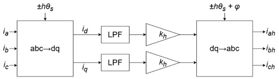
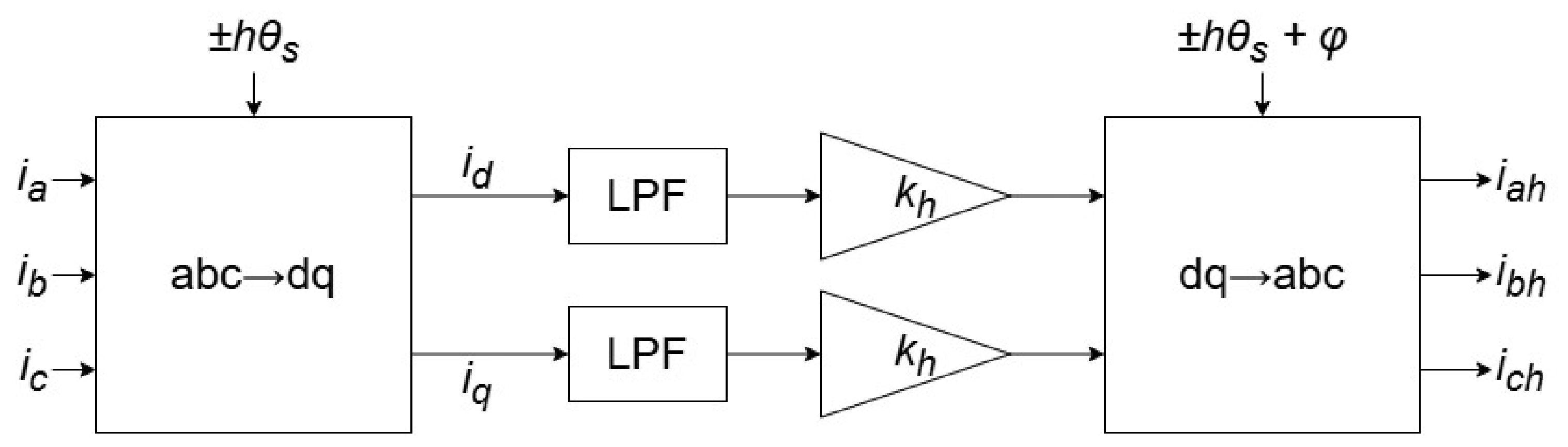
The harmonic current detection scheme is illustrated in Figure 8.
Figure 8.
Scheme of harmonic current detection.
The transfer function of the n-th order Butterworth low-pass filter is given by Equation (7):
where denotes the cutoff frequency of the filter, and K is the gain constant. Typically, is selected to achieve a unity DC gain.
The Butterworth low-pass filter exhibits balanced performance in terms of linear phase characteristics, attenuation slope, and loading characteristics. It provides fast dynamic tracking performance but relatively low steady-state accuracy. As the filter order increases, the steady-state error decreases, whereas the dynamic response time becomes longer. To achieve a compromise between steady-state accuracy and response speed, a second-order Butterworth filter is adopted in this paper.
Since the AC components in the power grid are periodic, using data within one fundamental-frequency cycle as the input of the filter can effectively eliminate the AC components in the signal. The transfer function of the mean filter is given by:
The mean filter has several advantages, including favorable cutoff frequency characteristics, stable detection results, fast dynamic response, and simple implementation using digital methods. However, it is sensitive to variations in the detected signal, and the filtering period needs to be determined according to the characteristics of the input signal. In addition, the mean filter introduces a certain time delay. When the calculation window length equals one fundamental-frequency cycle, the theoretical delay of the mean filter is 10 ms. To eliminate the influence of this delay, phase compensation is required during the inverse transformation when calculating the harmonic current. The compensation angle is given by .
Using only a Butterworth low-pass filter makes it difficult to simultaneously satisfy the requirements for detection accuracy and dynamic response speed. Although the mean filter can achieve ideal detection accuracy and dynamic response under constant current conditions, it is significantly affected when the current varies [14]. To address this issue, a cascade structure consisting of a Butterworth low-pass filter and a mean filter is adopted as the low-pass filter for harmonic current detection in this paper. This approach mitigates the ripple in the output waveform that occurs when only the Butterworth low-pass filter is used, while maintaining good dynamic response performance. Compared with the case where only the mean filter is employed, the fluctuation of the output signal of the low-pass filter caused by variations in the fundamental component is effectively suppressed.
Harmonic Control Strategy
After the harmonic currents in the system are detected, the device generates harmonic currents of equal magnitude and opposite phase to partially or completely cancel the existing current harmonics, thereby suppressing them.
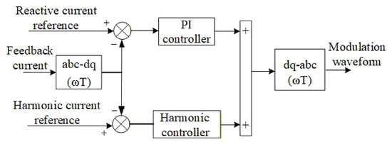
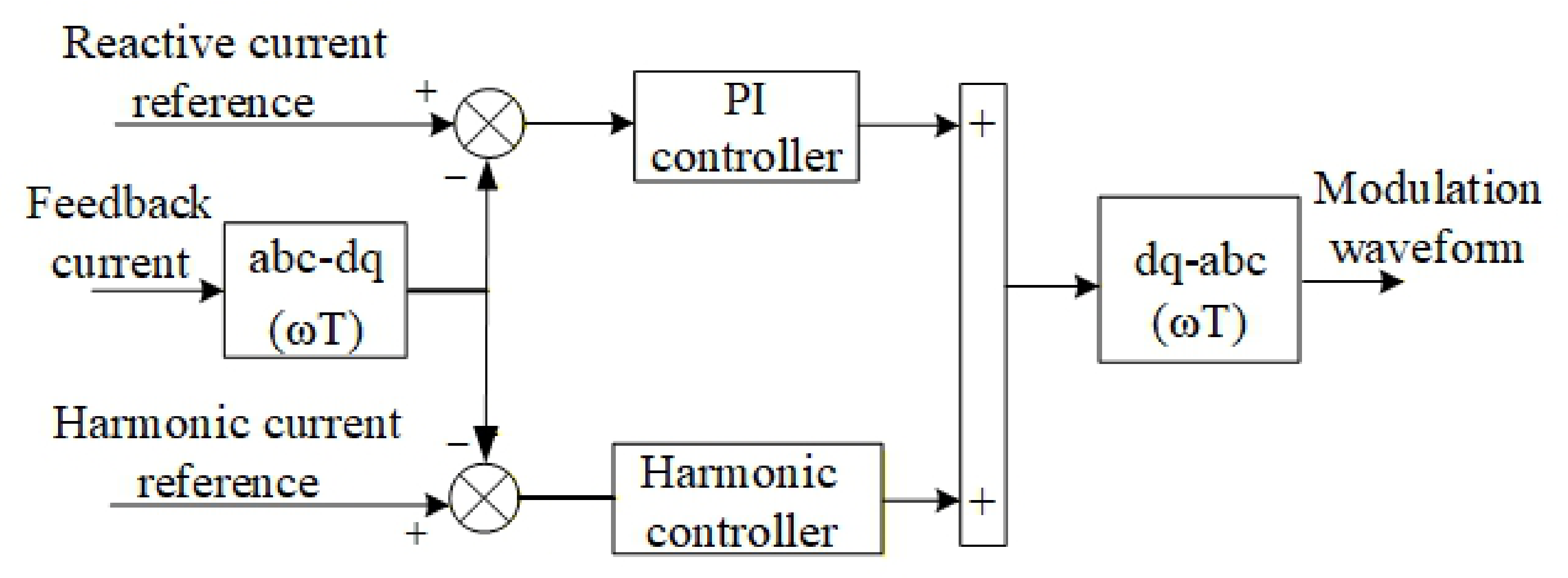
To realize a harmonic control strategy with low computational burden, harmonic control is implemented in the rotating dq reference frame in this paper. After the fundamental positive-sequence dq transformation, the 5th-order negative-sequence harmonic and the 7th-order positive-sequence harmonic are both converted into 6th-order harmonic components. Similarly, the 11th-order negative-sequence harmonic and the 13th-order positive-sequence harmonic are both converted into 12th-order harmonic components. Therefore, the 5th negative-sequence and 7th positive-sequence harmonics can be regulated using a unified 6th-order harmonic controller, while the 11th negative-sequence and 13th positive-sequence harmonics can be regulated using a unified 12th-order harmonic controller, thereby reducing the number of required controllers.
The designed control strategy is illustrated in Figure 9. After separating the fundamental current reference and the harmonic current reference, they are controlled independently. On the basis of the fundamental steady-state control function, a harmonic current control function is superimposed. These two control loops operate without mutual interference, which improves the flexibility and scalability of the overall control strategy.
Figure 9.
Block diagram of the harmonic control strategy.
Specific harmonic compensation is commonly implemented using resonant controllers [15], which can generally be classified into two types: the conventional resonant controller and the vector resonant controller [16]. Compared with the conventional resonant controller, the vector resonant controller can provide higher gain at the specified resonant frequency, enabling more accurate compensation of specific harmonic components. In addition, the bandwidth can be flexibly adjusted by tuning the controller parameters.
To accommodate possible grid frequency deviations, is introduced into the transfer function of the vector resonant controller, resulting in a quasi-vector resonant controller. Its transfer function is expressed as:
In Equation (9), denotes the proportional gain, denotes the resonant gain, and represents the fundamental angular frequency.
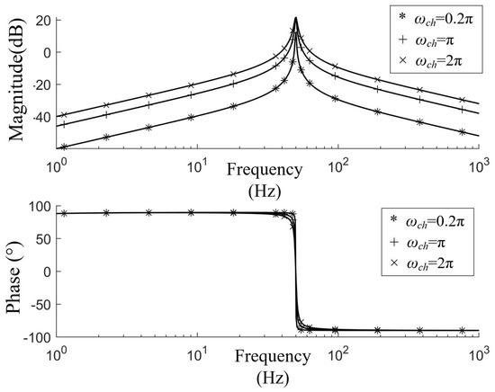
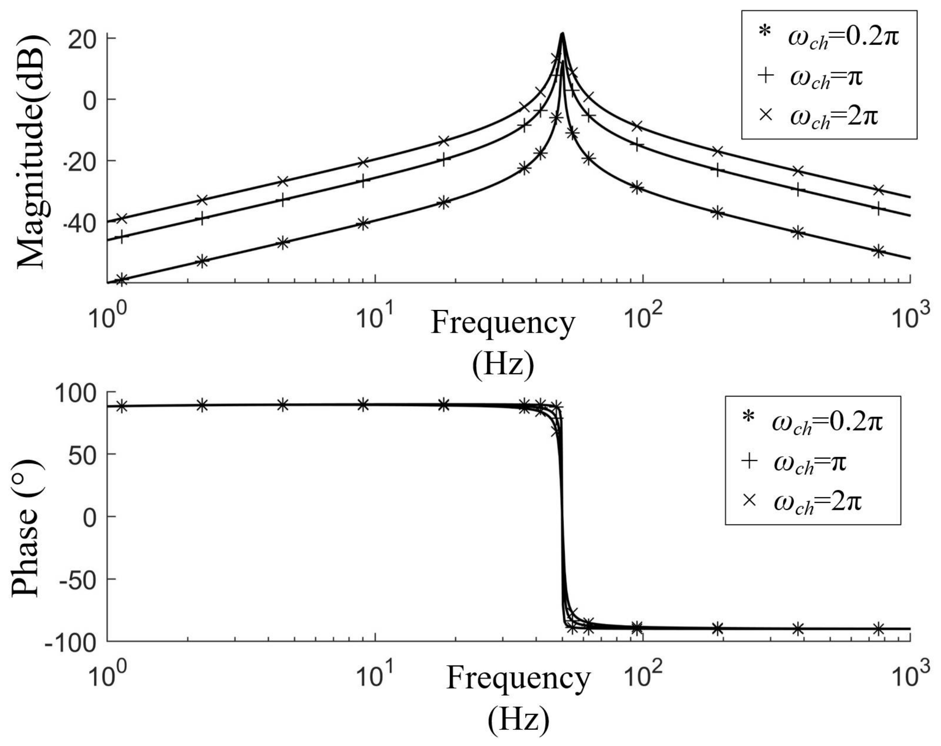
During parameter design, the differential term of the controller satisfies of the controlled plant [16]. Therefore, this paper focuses on the analysis of the parameters and , while the parameter is not further discussed.
The influence of on the frequency characteristics of the controller is illustrated in Figure 10. It can be observed that does not affect the gain at the resonant frequency in the amplitude–frequency characteristic, but it does affect the bandwidth. As increases, the bandwidth becomes larger, and the gain on both sides of the resonant frequency (especially on the right side) increases, resulting in poorer frequency selectivity of the controller. Moreover, also influences the phase–frequency characteristics near the resonant frequency. A larger results in a greater phase shift around the resonant frequency.
Figure 10.
Influence of on the frequency characteristics.
The influence of on the frequency characteristics of the controller is illustrated in Figure 11. It can be observed that as increases, the gain increases not only at the resonant frequency but also on both sides of the resonant frequency, resulting in poorer frequency selectivity. In addition, does not affect the phase–frequency characteristics.
Figure 11.
Influence of on the frequency characteristics of the controller.
From the above analysis, the vector resonant controller exhibits a band-pass characteristic. By selecting appropriate parameters, the controller can provide sufficient gain only at the resonant frequency while maintaining zero phase shift after the resonant frequency point, thus avoiding phase lag. Consequently, selective control of specific frequency components can be achieved, making the controller suitable for systems with inherent control delay.
Based on the above frequency-domain analysis, the quasi-vector resonant controller is tuned as follows. (i) Select the resonant bandwidth : a smaller improves frequency selectivity but weakens tolerance to grid-frequency drift, whereas a larger enhances dynamic rejection at the expense of selectivity. In this work, is chosen to balance selectivity against the typical grid-frequency deviation, and for the h-th harmonic the resonant bandwidth scales as . (ii) Choose the resonant gain to realize a target resonant-peak gain (10 dB in this paper) that ensures steady-state tracking accuracy without compromising selectivity. (iii) Determine the proportional gain from the plant constraint . This three-step procedure can be formulated as a multi-objective optimization that jointly considers tracking accuracy, selectivity, and robustness [10].
In the dq rotating reference frame, the resonant term introduces a pair of complex-conjugate poles located at with damping coefficient . Provided that the current-loop crossover frequency lies below , the resonant poles are situated well above the loop crossover; because the band-pass characteristic exhibits zero phase shift away from its narrow resonant band (as shown above), it introduces negligible additional phase lag near crossover, so the phase margin of the original current loop is essentially preserved. Together with the plant-matched proportional gain in step (iii), the chosen and thus endow the current loop with robustness against variations in the plant parameters L and R.
5. Experimental Analysis
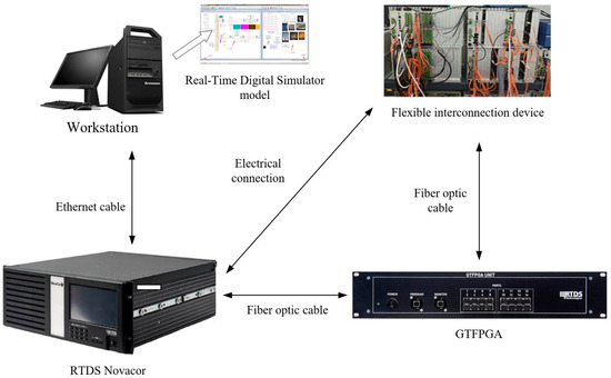
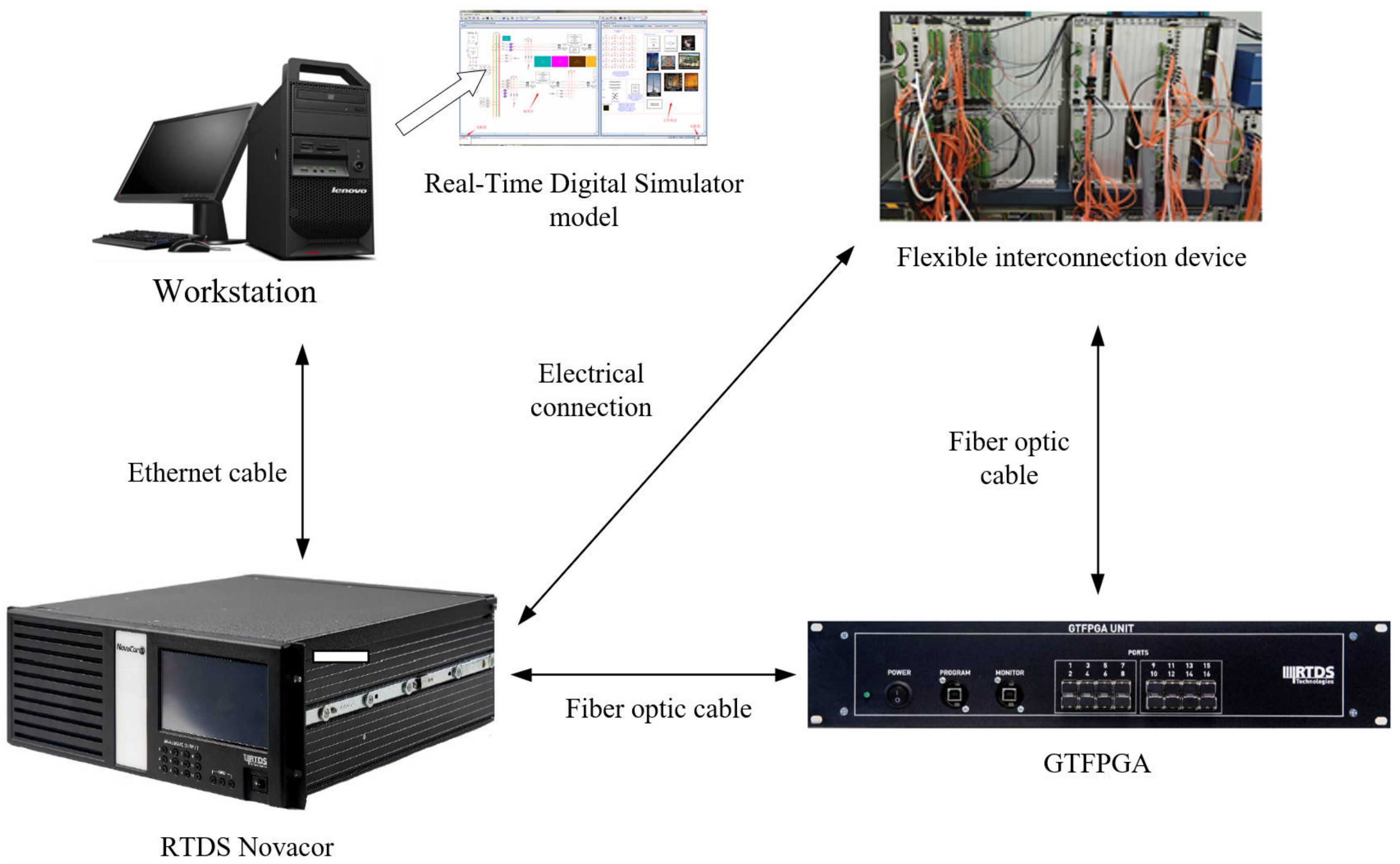
To verify the effectiveness of the proposed harmonic control strategy, an RTDS-based experimental platform of a 10 kV/5 MW medium-voltage flexible interconnection device was established, as shown in Figure 12. The RTDS test system consists of an RTDS rack, an RTDS simulation model, a flexible interconnection device controller, a GTFPGA, and a workstation.
Figure 12.
Hardware-in-the-loop test platform of the medium-voltage flexible interconnection device.
The main circuit model of the flexible interconnection device runs on the GTFPGA hardware, while the controller of the flexible interconnection device sends pulse commands to the GTFPGA via optical fiber and receives capacitor voltage data of each power module in the main circuit through optical fiber communication. The grid-side model operates in the RTDS rack. The controller of the flexible interconnection device communicates with the RTDS rack through electrical hardwiring for analog signals and digital input/output signals. The workstation acts as the host computer to issue control commands and monitor the waveform data of the device.
The parameters listed in Table 1 correspond to the rated specifications of the actual medium-voltage flexible interconnection device developed in the engineering project, rather than being re-derived within this paper. The overall parameters (rated power of 5 MW and rated voltage of 10 kV) are determined by the grid-connection requirements of the demonstration site. The number of power modules per arm (12 ) and the main-line reactance (7 mH) follow the converter-level design adopted in the project to meet the required output voltage levels and current-ripple limits. The power-module parameters, including the module rated voltage (900 V) and capacity (150 kW), are selected according to the voltage and current ratings of the adopted power semiconductors and the power-module power allocation. The carrier frequencies of the H-bridge (300 Hz) and the DAB stage (10 kHz) are chosen from the trade-off between switching loss and output performance in the project implementation. The DC-link capacitance (3 mF) and the DAB resonant components (, , , and a high-frequency transformer turns ratio of 1 kV/1 kV) are specified by the resonant converter design of the project to achieve the required voltage ripple, voltage gain, and soft-switching operation.
Table 1.
Parameters of the medium-voltage flexible interconnection device.
The quasi-vector resonant controllers used in the medium-voltage flexible interconnection device have a resonant bandwidth of , which ensures that the controller achieves high frequency selectivity while maintaining good disturbance rejection. The resonant gain is set to achieve an amplitude of 10 dB at the resonant peak, ensuring sufficient gain at the controlled frequency while preserving frequency selectivity. Based on these settings, the 6th-order harmonic controller has a resonant bandwidth of and a resonant gain of . Similarly, the 12th-order harmonic controller has a resonant bandwidth of and a resonant gain of . These settings follow the three-step tuning rule described above and preserve the phase margin of the current loop while delivering the required resonant gain.
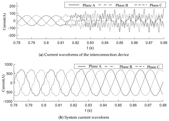
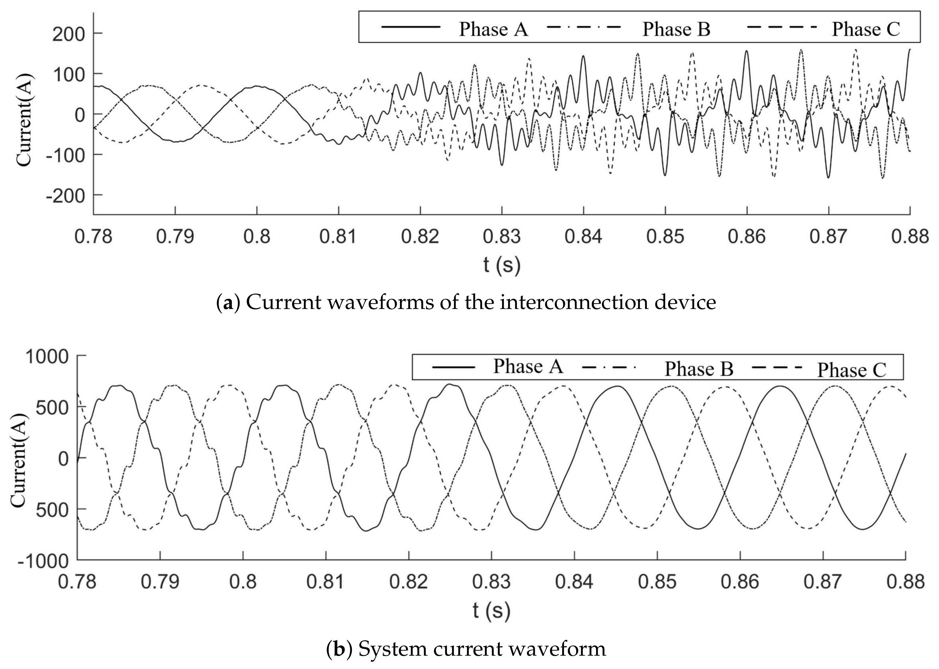
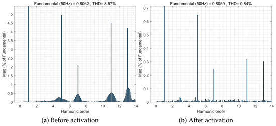
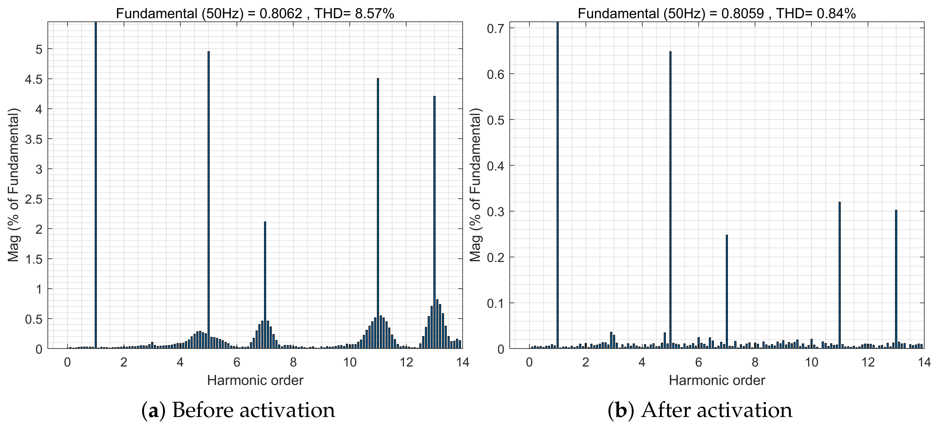
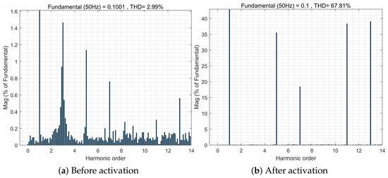
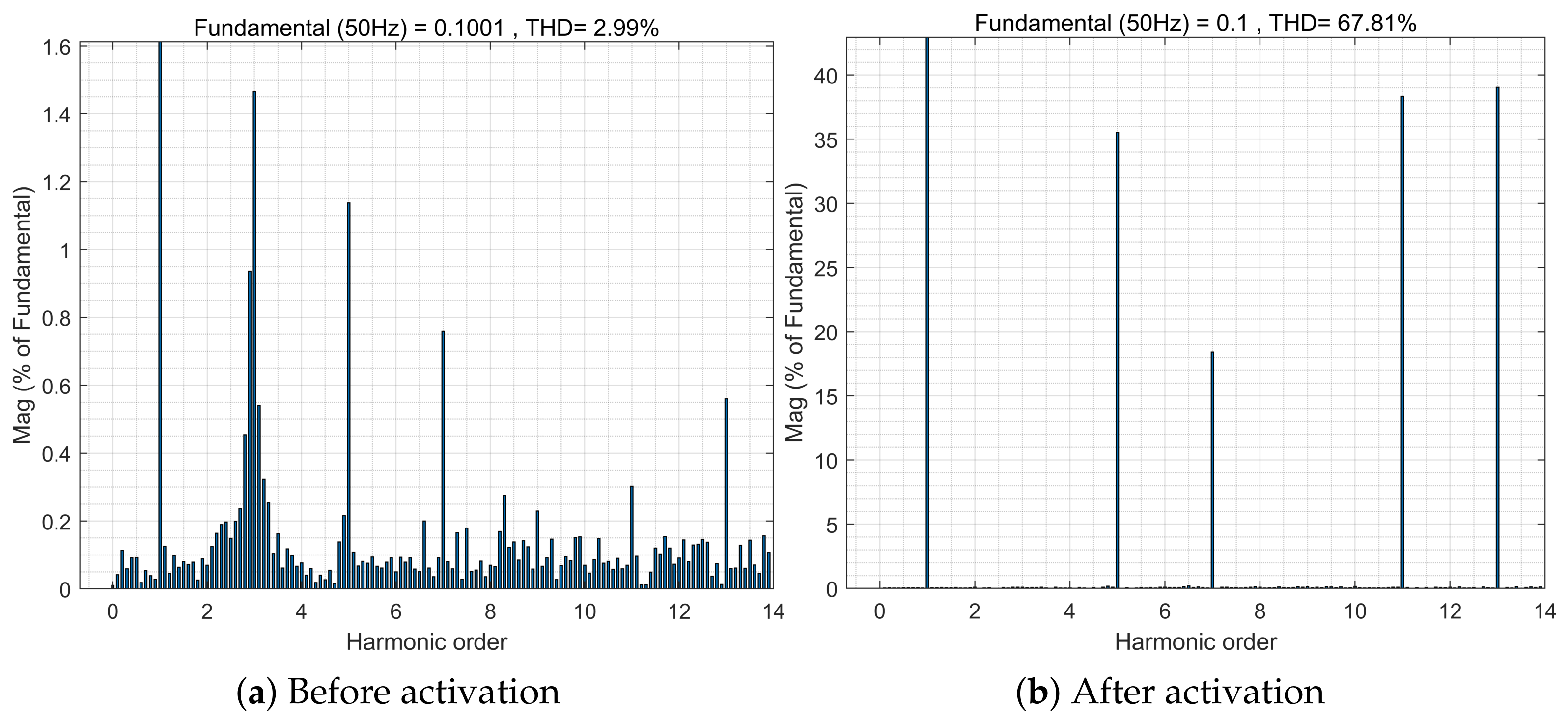
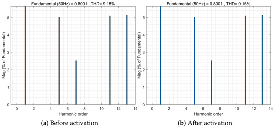
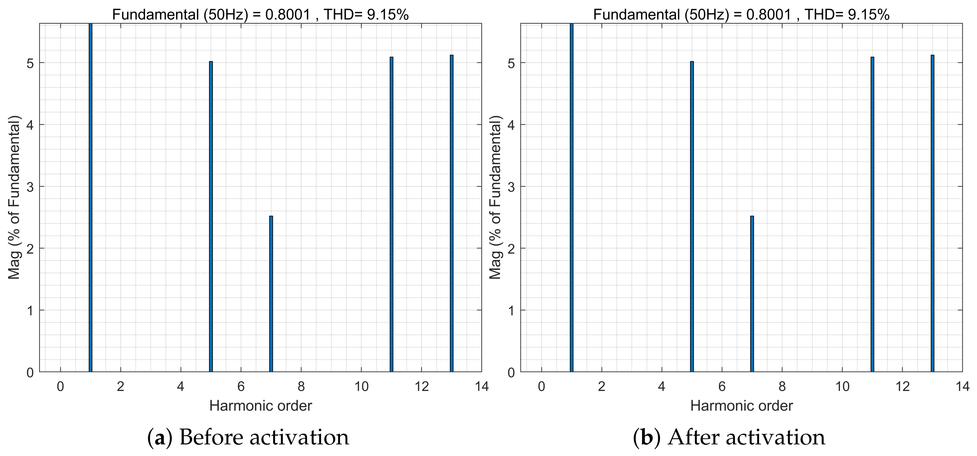
Figure 13 shows the currents of the flexible interconnection device and the system before and after activating the harmonic current compensation control function. Figure 14, Figure 15 and Figure 16 present the harmonic-spectrum comparisons of the grid (system) current, the compensation-device current, and the load current before and after activation, respectively, with the corresponding harmonic-content data summarized in Table 2, Table 3 and Table 4. As can be seen from the figures, at 0.8 s, after the harmonic compensation control function is activated, the flexible interconnection device begins to perform harmonic compensation, and the harmonics in the system current are effectively suppressed.
Figure 13.
Waveform during activation of the harmonic current compensation function: (a) current waveforms of the interconnection device; (b) system current waveform.
Figure 14.
Harmonic spectrum of the grid (system) current before and after activating the harmonic current compensation function.
Figure 15.
Harmonic spectrum of the compensation-device current before and after activating the harmonic current compensation function.
Figure 16.
Harmonic spectrum of the load current before and after activating the harmonic current compensation function.
Table 2.
Grid (system) current harmonic content before and after activating the harmonic current compensation function. The THD drops from 8.57% to 0.84% (a reduction of about 90.2%).
Table 3.
Compensation-device current harmonic content before and after activating the harmonic current compensation function.
Table 4.
Load current harmonic content before and after activating the harmonic current compensation function.
The high THD of the device current is expected, as the device intentionally injects counter-phase harmonic currents to cancel the same-order harmonics in the grid current. Therefore, the large harmonic content observed in the device current reflects its active compensation output rather than a control failure.
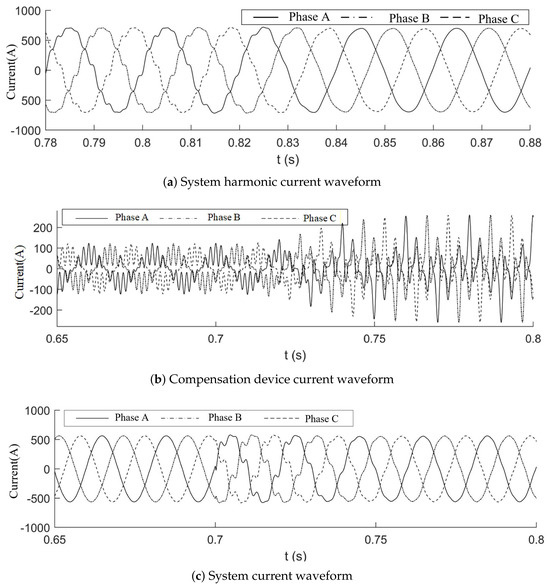
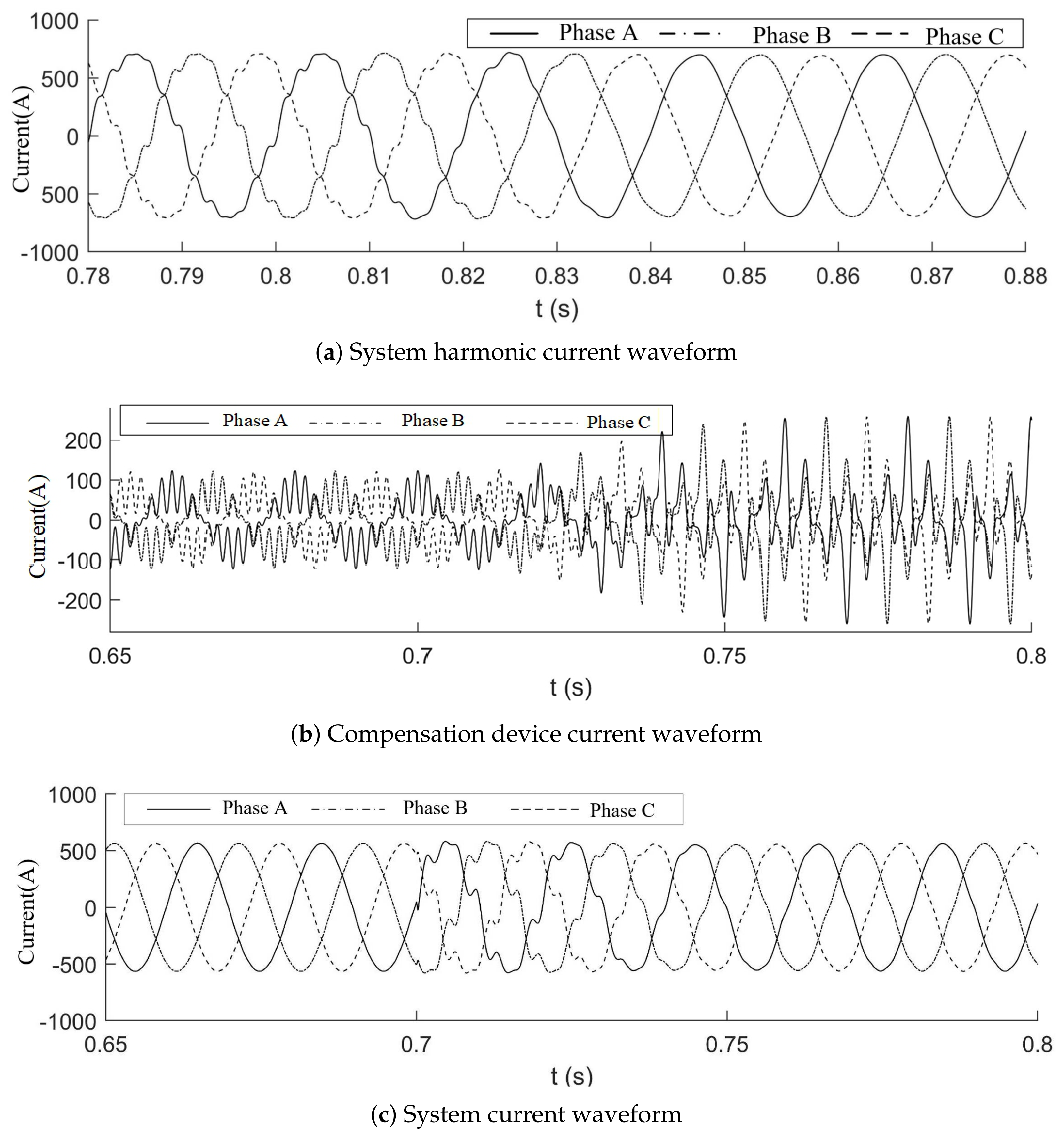
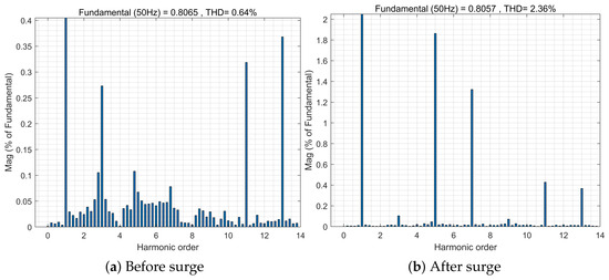
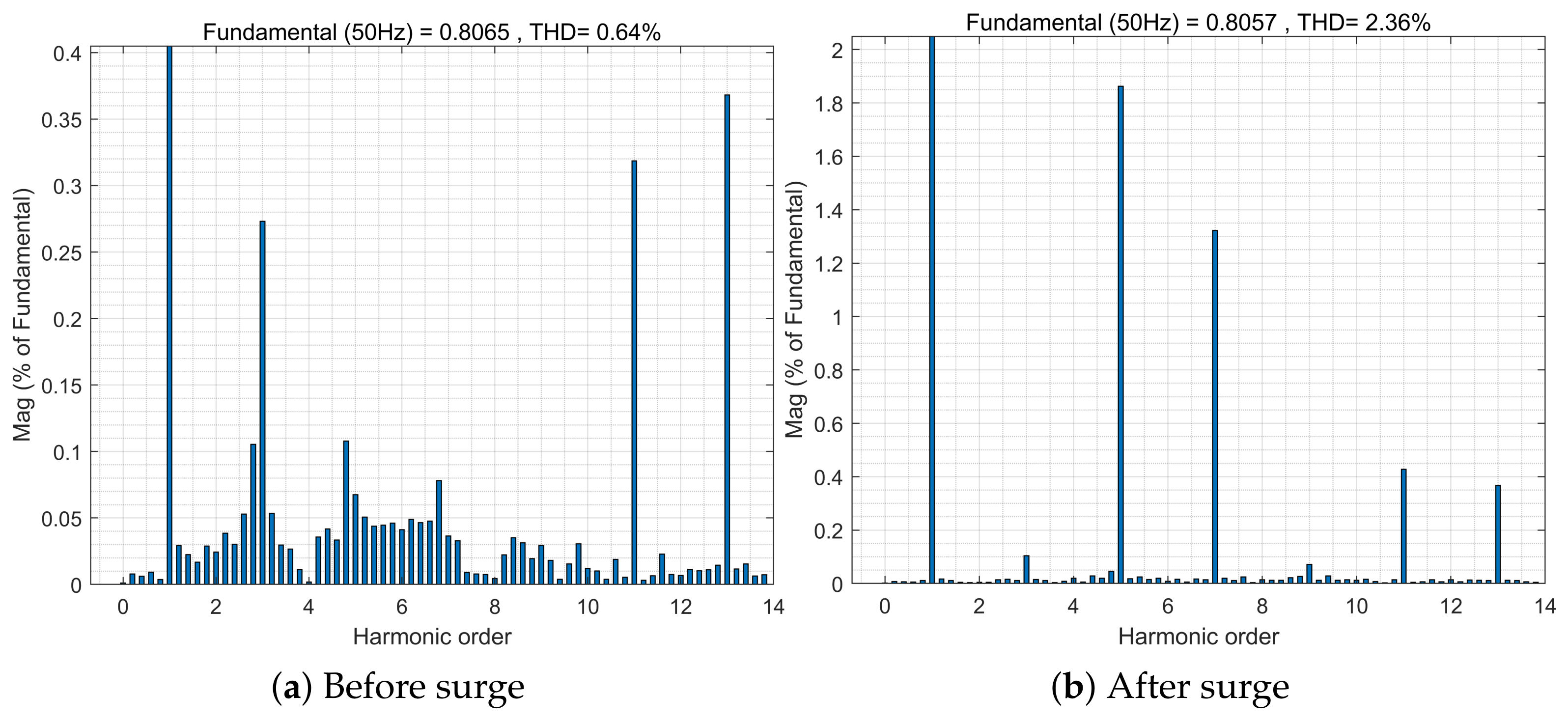
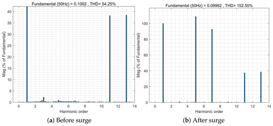
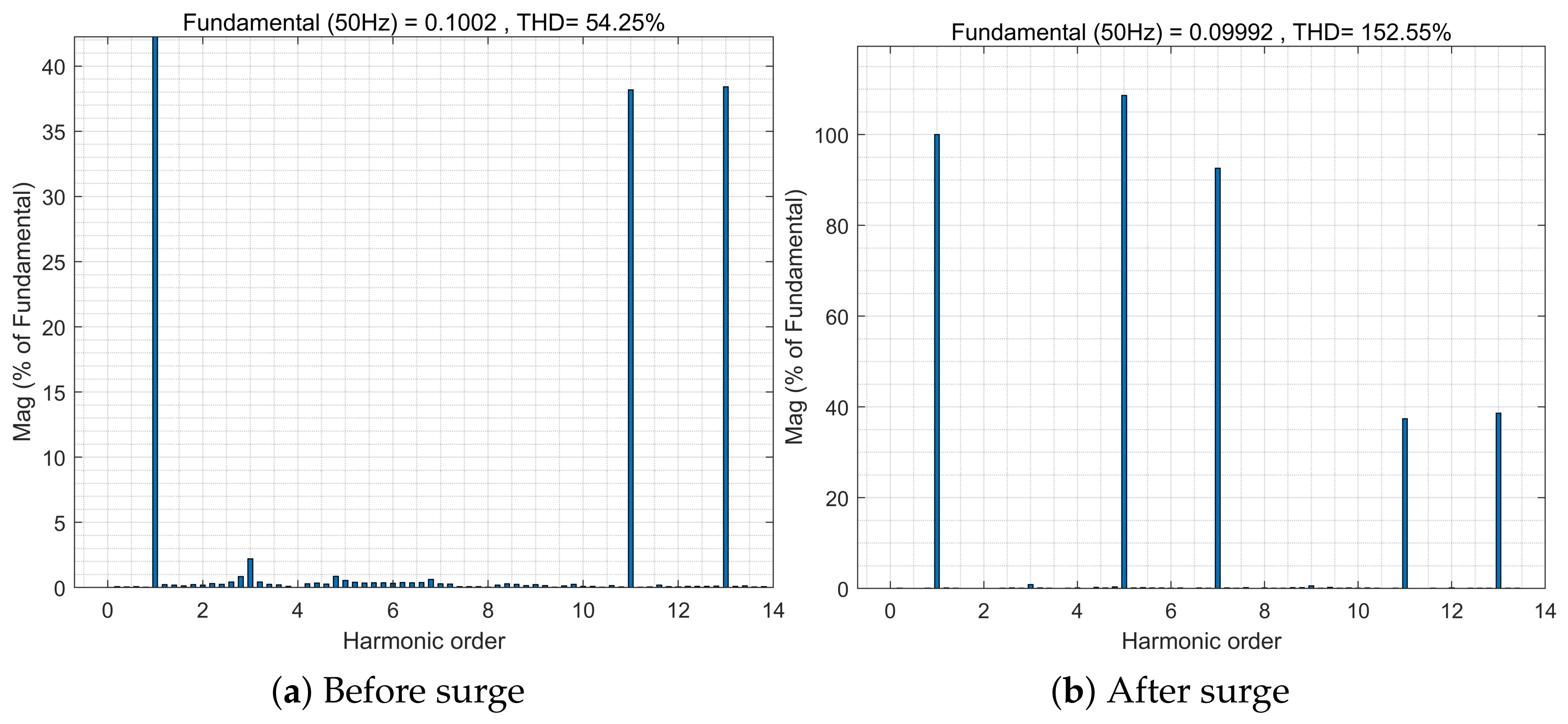
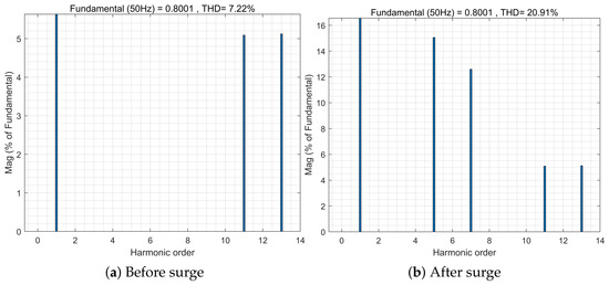
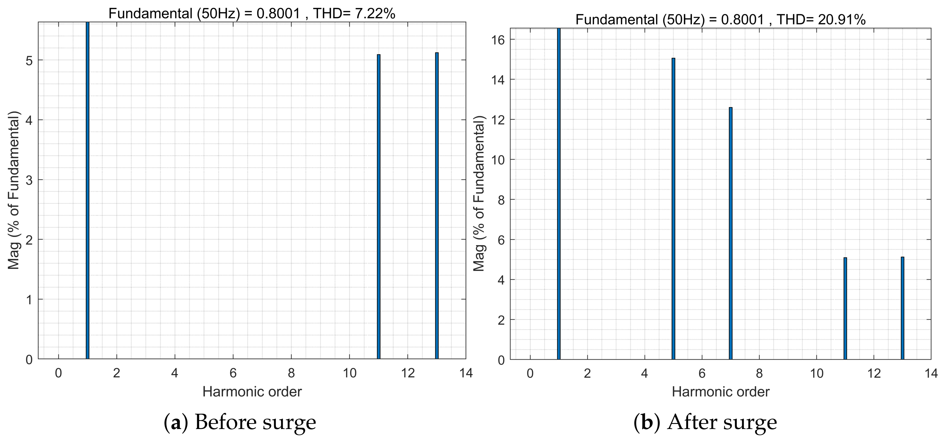
The surge test below is an independent experimental scenario, distinct from the activation test described above; the 0.7 s surge and the 0.8 s activation are not consecutive events. Figure 17 shows the waveform of a harmonic-current surge. As can be seen from the figure, at 0.7 s the system harmonic current suddenly increases. The flexible interconnection device rapidly tracks this variation: it is clearly observed that the harmonic-current tracking is completed within two fundamental cycles. Comparing the periods before and after the surge, the device effectively suppresses the surge harmonics in the system current. This is quantitatively corroborated by Figure 18, Figure 19 and Figure 20 and Table 5, Table 6 and Table 7. Although the surge raises the load-current THD from 7.22% to 20.9%, the system (grid) current THD stays low, increasing only from 0.64% to 2.36%. This confirms that the device responds to the surge by injecting large counter-harmonic currents—as reflected by the compensation-device current THD rising from 54.25% to 152.55%—thereby preventing the sudden 5th-/7th-order harmonics from significantly polluting the system side.
Figure 17.
Waveform of harmonic current surge: (a) system harmonic current waveform; (b) compensation device current waveform; (c) system current waveform.
Figure 18.
Harmonic spectrum of the grid (system) current before and after the harmonic current surge.
Figure 19.
Harmonic spectrum of the compensation-device current before and after the harmonic current surge.
Figure 20.
Harmonic spectrum of the load current before and after the harmonic current surge.
Table 5.
Grid (system) current harmonic content before and after the harmonic current surge. The system-current THD remains low (0.64% before and 2.36% after the surge), confirming effective suppression of the surge harmonics.
Table 6.
Compensation-device current harmonic content before and after the harmonic current surge.
Table 7.
Load current harmonic content before and after the harmonic current surge.
The RTDS hardware-in-the-loop test results confirm the effectiveness of the proposed strategy. After the harmonic compensation function is activated at 0.8 s, the system-current THD drops from 8.57% to 0.84% (a reduction of about 90.2%), with the per-order harmonic breakdown given in Table 2, Table 3 and Table 4. When a sudden harmonic-current surge occurs at 0.7 s, the device tracks the variation within two fundamental cycles, and the system-current THD stays low (0.64% before and 2.36% after the surge), even though the load-current THD rises to 20.9% and the device-current THD reaches 152.55% as it injects the counter-harmonic currents, as detailed in Table 5, Table 6 and Table 7. Together with the sub-two-cycle harmonic tracking, these metrics demonstrate that the proposed harmonic compensation control strategy effectively suppresses system-current harmonics and achieves fast dynamic response.
6. Conclusions
6.1. Contributions and Benefits
The main contributions of this paper are threefold. First, a novel star-connected topology for the medium-voltage flexible interconnection device is proposed, which integrates a compact power module based on a dual-active-bridge (DAB) three-stage structure with the star-connected interface. The star-connected arrangement and the compact DAB-based power module jointly improve modularity and provide galvanic isolation, which is advantageous for integrating feeders of different voltage levels within a single flexible interconnection device. The three-stage DAB structure further enhances power-transfer flexibility between the isolated ports. Second, a steady-state control strategy is designed to guarantee stable operation of the device under high background harmonics. Third, a harmonic current compensation control strategy together with a corresponding quasi-vector resonant controller parameter-design method is proposed, enabling the 5th/7th and 11th/13th harmonics to be suppressed by unified 6th- and 12th-order resonant controllers, respectively.
6.2. Limitations and Future Work
Despite the promising results, several limitations should be acknowledged. First, the validation is performed on an RTDS hardware-in-the-loop platform rather than in a real grid environment; the influence of non-ideal grid conditions on the field performance remains to be verified. Second, no quantitative comparison with alternative harmonic-compensation methods is provided. Third, the analysis of the DC-voltage balancing strategy and the hybrid modulation is currently qualitative; a closed-loop transfer-function analysis is left for future work.
Future work will address these limitations by (i) conducting a formal closed-loop stability analysis of the DC-voltage balancing loop, (ii) performing comparative experiments against baseline harmonic-compensation methods, and (iii) validating the strategy on a physical prototype to confirm its performance under practical grid disturbances.
Author Contributions
Conceptualization, Q.L.; methodology and software, Q.L.; investigation and data curation, F.Z.; writing—original draft preparation, X.Y.; writing—review and editing, X.Y. All authors have read and agreed to the published version of the manuscript.
Funding
This research received no external funding.
Data Availability Statement
The data used in this study are derived from actual engineering experience values and simulation-generated results, and are contained within the article.
Conflicts of Interest
The authors declare no conflicts of interest.
References
- Yang, D.; Wu, Y.; Pandzic, H.; Tomin, N. Fault recovery of active distribution network considering translatable load and soft open point. J. Electr. Power Sci. Technol. 2024, 39, 183–192. [Google Scholar] [CrossRef]
- Yin, W.; Feng, S.; Liu, R.P.; Hou, Y. Chance-constrained co-expansion planning for power systems under decision-dependent wind power uncertainty. IET Renew. Power Gener. 2023, 17, 1342–1357. [Google Scholar] [CrossRef] [Scilit]
- Kamyab, G.R. Power distribution system restoration based on soft open points and islanding by distributed generations. Int. J. Emerg. Electr. Power Syst. 2025, 26, 745–766. [Google Scholar] [CrossRef] [Scilit]
- Li, S.; Liu, M.; Liu, C. Multi-terminal flexible interconnection for distribution networks using VSC-based hybrid bidirectional power converter. Electronics 2026, 15, 1602. [Google Scholar] [CrossRef] [Scilit]
- Wang, Z.; Liu, G.; Pang, D.; Wang, Y.; Yu, B.; Wang, Z. Optimal operation of flexible interconnected distribution grids based on improved virtual synchronous control techniques. Front. Energy Res. 2024, 12, 1356227. [Google Scholar] [CrossRef] [Scilit]
- Xiao, Z.; He, Z.; Wang, H.; Luo, A.; Shuai, Z.; Guerrero, J.M. General high-frequency-link analysis and application of dual active bridge converters. IEEE Trans. Power Electron. 2020, 35, 8673–8688. [Google Scholar] [CrossRef] [Scilit]
- Li, X.; Guo, L.; Li, Y.; Hong, C.; Zhang, Y.; Guo, Z.; Huang, D.; Wang, C. Flexible interlinking and coordinated power control of multiple DC microgrids clusters. IEEE Trans. Sustain. Energy 2017, 9, 904–915. [Google Scholar] [CrossRef] [Scilit]
- Sun, Y.; Zhang, J.; Zhou, J.; Shi, G.; Yang, X.; Cai, X. A novel multiport flexible interconnection switch for AC/DC hybrid distribution network. Proc. CSEE 2023, 43, 5151–5163. [Google Scholar] [CrossRef]
- Xie, L.; Zeng, S.; Liu, J.; Zhang, Z.; Yao, J. Control and stability analysis of the LCL-type grid-connected converter without phase-locked loop under weak grid conditions. Electronics 2022, 11, 3322. [Google Scholar] [CrossRef] [Scilit]
- Ye, J.; Huang, S.; Huang, Y.; Hu, Y.; Zhang, C.; Xu, J.; Shen, A. A new parameter tuning method for generalized multiresonant current controllers in grid-connected inverters. IEEE Trans. Power Electron. 2024, 39, 10962–10975. [Google Scholar] [CrossRef] [Scilit]
- Guo, J.; Fan, T.; Li, Q.; Wen, X. An angle-compensating, complex-coefficient PI controller used for decoupling control of a permanent-magnet synchronous motor. Symmetry 2022, 14, 101. [Google Scholar] [CrossRef] [Scilit]
- Ansari, M.S.; Shukla, A.; Bahirat, H.J. Analysis and design of MMC-based high-power DC-DC converter with trapezoidal modulation. IEEE Trans. Power Electron. 2023, 38, 7256–7270. [Google Scholar] [CrossRef] [Scilit]
- Chen, J.; Zhao, T.; Xu, Y.; Tao, Y.; Wang, C.; Sun, Q. A hybrid modulation strategy for MMC with controllable quantization error. J. Electr. Power Sci. Technol. 2023, 38, 105–113. [Google Scholar] [CrossRef]
- Kumar, A.N.; Raglend, I.J. Multi-objective control of multi-operational grid-integrated inverters for PV integration and power quality services. Ain Shams Eng. J. 2021, 12, 2859–2874. [Google Scholar] [CrossRef] [Scilit]
- Lunardi, A.; Normandia Lourenco, L.F.; Munkhchuluun, E.; Meegahapola, L.; Sguarezi Filho, A.J. Grid-connected power converters: An overview of control strategies for renewable energy. Energies 2022, 15, 4151. [Google Scholar] [CrossRef] [Scilit]
- Sunbul, A.; Alduraibi, A.; Zare, F. Harmonics mitigation filter for high-power applications. IEEE Access 2022, 10, 111406–111418. [Google Scholar] [CrossRef] [Scilit]

Disclaimer/Publisher’s Note: The statements, opinions and data contained in all publications are solely those of the individual author(s) and contributor(s) and not of MDPI and/or the editor(s). MDPI and/or the editor(s) disclaim responsibility for any injury to people or property resulting from any ideas, methods, instructions or products referred to in the content. |
© 2026 by the authors. Licensee MDPI, Basel, Switzerland. This article is an open access article distributed under the terms and conditions of the Creative Commons Attribution (CC BY) license.