


Abstract
The paper presents an analytical study and small-signal modeling of a non-inverting two-switch buck–boost converter based on the LM5118 controller, accounting for parasitic elements. The converter dynamics were analyzed using simulations in the PLECS® 5.0.2 environment. Furthermore, the steady-state and dynamic characteristics of the LM5118-based two-switch buck–boost converter were examined using the PSpice for TI® simulator for different input voltages and load conditions. The obtained simulation results show close correspondence with the analytical analysis, confirming the validity of the proposed approach.
1. Introduction
The development of modern energy and electronic systems is closely linked to the need for the efficient management and conversion of electrical energy. In this context, DC–DC converters are a critical type of power electronics device that adjusts voltage levels to meet the needs of different loads and electronic systems [1]. They are used in switching power supplies, renewable energy systems, electric vehicles, telecommunications equipment, and autonomous power systems, among other applications.
Particular attention is paid to converters designed for hybrid energy systems, which require the efficient management of energy flow between different sources and storage devices [2,3,4,5,6]. In addition to these solutions, simpler, non-isolated topologies are of interest because they allow the output voltage to be stepped up or down relative to the input voltage. These topologies are known as buck–boost converters and are widely used in systems where the input voltage varies widely. However, classic buck–boost structures often have high voltage stresses on the switching elements and unfavorable dynamic properties under certain operating conditions [7].
In practice, advanced topologies are used, including the two-switch buck–boost converter. This converter is a modified switching converter structure with two active switching elements. This configuration enables better control of energy flow, reduced stress on power switches, and improved conversion efficiency. Additionally, this topology enables more flexible control of the operating mode and better integration with modern control systems [8,9,10,11].
It enables better control of the power flow, reduces stress on the power switches, and improves conversion efficiency. Modern DC–DC converters are often controlled by specialized integrated controllers that combine regulation, protection, and optimization functions for the system’s dynamic characteristics. Many manufacturers offer such control solutions for buck–boost and similar topologies. Examples of these controllers include the LTC3780 from Analog Devices [12], the TPS63060 from Texas Instruments [13], and the ISL9110 from Renesas Electronics [14]. In this study, the converter is controlled by the LM5118 integrated controller, which is designed to control non-inverting buck–boost DC–DC converters with a wide input voltage range. The LM5118 implements current-mode control with an emulated current ramp, improving system stability and simplifying the compensation network design [15]. The LM5118 drives two external MOSFETs and enables a smooth transition between buck and buck–boost modes depending on the input-to-output voltage ratio.
Despite its advantages, the two-switch buck–boost converter’s dynamic behavior is characterized by complex relationships among its electrical parameters, switching modes, and control signals. To analyze and design the control system, it is necessary to develop an adequate mathematical model that describes the system dynamics around the steady-state operating mode. One widely used approach for analyzing power electronic converters is the state-space averaging method, which describes the system dynamics using a linearized model. Using this method, transfer functions can be obtained to describe the relationship between the control and electrical variables in the converter.
The main objective of this study is to analyze and simulate the effects of active component losses on the operation of a non-inverting two-switch buck–boost converter on its main transfer functions. In studying the converter’s operation, a combined modeling approach using PLECS® 5.0.2 and PSpice for TI® 2024 is applied, as these tools offer complementary capabilities for modeling power electronic systems and analog control circuits [16,17]. The typical characteristics of the converter controlled by the LM5118 are investigated using the PSpice for TI® simulator at various input voltages and loads, while the investigation of the main transfer functions describing the dynamic relationship between the control and electrical parameters of the system is based on the PLECS® simulator.
2. Two-Switch Buck–Boost Converter Operation Principle
2.1. Main Circuit Operation
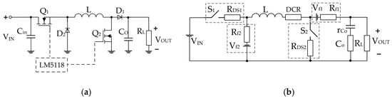
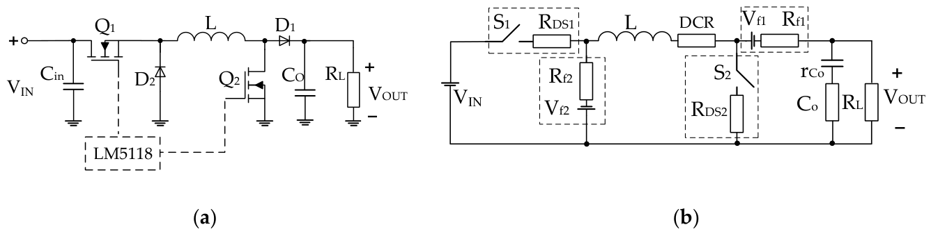
Figure 1 shows the studied a non-inverting two-switch buck–boost DC–DC converter (TSBBC) implemented using two MOSFETs, Q1 and Q2, diodes D1 and D2, an inductor L, an input filter capacitor Cin, an output filter capacitor CO, and a load resistor RL. The following parameters are defined: fs—switching frequency; and D—duty cycle. The power stage is controlled by the LM5118 integrated controller, which generates control signals for the two external transistors (Q1 and Q2) and provides output-voltage regulation via current-mode control.
Figure 1.
Non-inverting two-switch buck–boost converter: (a) main circuit; (b) equivalent circuit including parasitics.
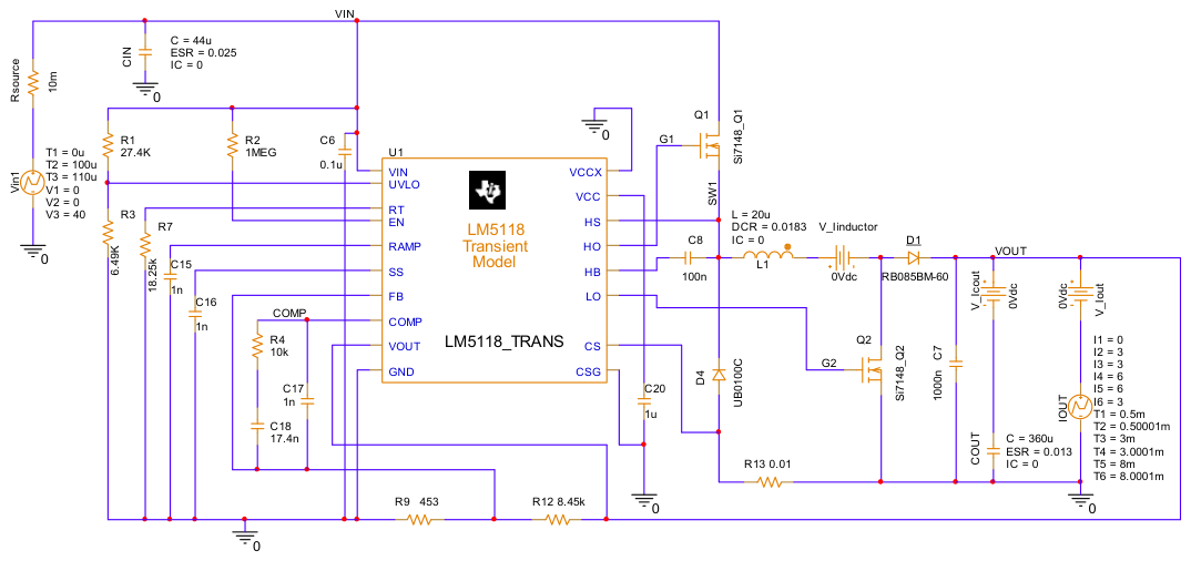
Figure 2 shows the equivalent circuit, including the parasitic components, as follows: the on-resistances of the two MOSFETs (RDS1 and RDS2); the forward resistances of the two diodes (Rf1 and Rf2); Vf1 and Vf2, the voltage drop of D1 and D2; the inductor direct current resistance (DCR); and the output capacitor’s equivalent series resistance (ESR) rCo.
Figure 2.
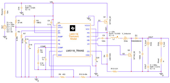
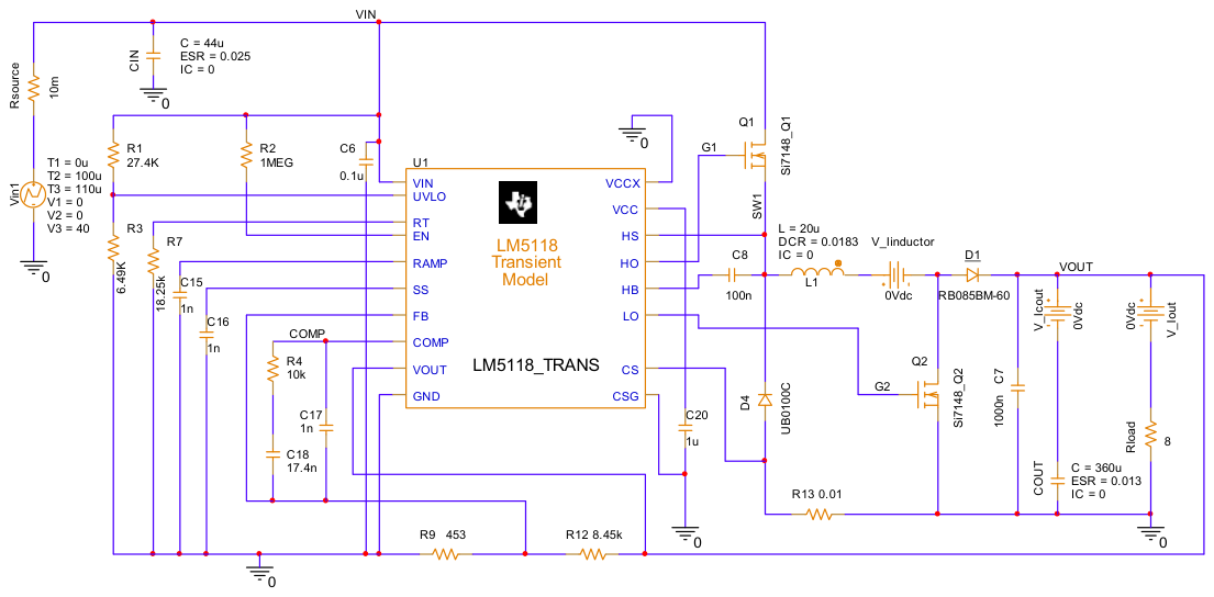
PSpice for TI simulation circuit for a two-switch buck–boost converter (TSBBC) based on the LM5118 controller, Texas Instruments, Dallas, TX, USA.
The non-inverting DC–DC buck–boost converter regulates the output voltage VOUT, which can be lower or higher than the input voltage VIN while maintaining the same polarity as at the input.
The converter can operate in different modes depending on the ratio between the input voltage (VIN) and the output voltage (VOUT). When the input voltage VIN is sufficiently greater than the output voltage VOUT, the system operates primarily as a step-down converter (buck mode). As the input voltage, VIN, approaches the output voltage, it smoothly transitions into buck–boost mode [15]. Thanks to the LM5118 controller, the transition between these modes is smooth, ensuring continuous output-voltage regulation and stable operation over a wide range of input conditions.
The controller enables the converter to continue operating as a standard buck regulator initially, with only transistor Q1 active, when the input voltage decreases toward the output voltage. To maintain a stable output voltage, the controller increases its duty cycle. Once the duty cycle reaches approximately 75%, the controller activates the second transistor (Q2) with a very small duty cycle. This marks the beginning of transition mode. As the input voltage continues to decrease, the duty cycle of Q2 gradually increases, while that of Q1 gradually decreases [15].
For the buck mode, the ideal DC voltage gain in CCM (efficiency η = 1) is equal to [1]:
The real voltage gain () for the buck mode, considering parasitic resistances in continuous conduction mode (CCM), can be expressed as follows:
For the buck–boost mode, the ideal DC voltage gain in CCM (efficiency η = 1) is equal to [1]:
The real voltage gain () for the buck–boost mode, considering parasitic resistances in continuous conduction mode (CCM), can be expressed as follows:
The presence of parasitic resistances reduces the real voltage gain to below the ideal conversion ratios (1) and (3). This reduction can be represented by a coefficient smaller than unity, whose magnitude is governed by the relationship between the resistive losses and the load resistance RL. With a constant RL, higher parasitic resistances limit the maximum achievable voltage gain.
2.2. Two-Switch Buck–Boost Converter Based on LM5118 Controller
In this paper, the control of a non-inverting two-switch buck–boost converter is implemented using the LM5118 controller. The controller provides control via pulse-width modulation (PWM), drivers for the external MOSFET transistors, and additional functions such as soft start, undervoltage lockout protection, and current limiting.
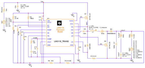
Figure 2 shows the model of the circuit under study in the PSpice for TI simulator [17].
The controller is supplied via the VIN pin, with the internal regulator providing the necessary power for the control logic and drivers. The VCCX pin serves as an input for an external power supply for the gate drivers. The VCCX pin can be connected to ground. In this case, the transistor drivers are powered by the internal regulator (VCC). Startup and protection of the converter are controlled by the undervoltage lockout (UVLO) circuit. The minimum input voltage required to activate the controller is set by the R1, R3 divider. The EN (Enable) pin allows external enable/disable of the converter and provides control over the startup process. Resistor R7, connected to the RT pin, sets the switching frequency and determines the internal oscillator frequency.
The operating frequency of the controller is determined by an external resistor R7 using equation [15]:
The LM5118 controller uses emulated current-mode control. An external capacitor, C15, connected to the RAMP pin, sets the slope of the current ramp used in the PWM comparator. This signal ensures control stability and provides slope compensation at high duty cycles.
The output voltage is regulated via a feedback network connected to the FB pin. The resistive divider formed by R12 and R9 measures the output voltage and compares it to the controller’s internal reference voltage. The difference between the feedback voltage and the reference voltage is processed by the internal error amplifier, whose output is available at the COMP pin. The dynamic characteristics of the control loop are determined by the external compensation circuit R4, C17, and C18, connected to this pin. The compensation circuit shapes the control loop’s frequency response and ensures sufficient phase margin and system stability across the entire operating range. Current limiting is achieved via the CS pin, which monitors the current in the converter’s power section.
The following design considerations should be taken into account when designing TSBBC based on the LM5118, as shown in Table 1 [15].
Table 1.
LM5118 two-switch buck–boost converter design considerations.
3. Two-Switch Buck–Boost Converter Small-Signal Transfer Functions
3.1. Two-Switch Buck–Boost Converter Control-to-Output Transfer Function
The DC gain relationships derived from (1–4) describe the converter’s observed behavior in various operating modes. However, they are insufficient for evaluating its dynamic characteristics. Switching to small-signal modeling is necessary to analyze the system’s response to small disturbances around the selected operating point.
Transfer function analysis is important because it provides information about a system’s frequency characteristics, stability, and sensitivity to input and load disturbances. These functions form the basis for synthesizing controllers and optimizing the converter’s dynamic response. Therefore, analytically deriving and analyzing the transfer functions of a two-switch buck–boost converter is a crucial step in designing effective control systems and evaluating its dynamic characteristics.
The relationship between a small variation in the duty cycle and the corresponding change in the output voltage is examined. When analyzing the control-to-output transfer function, Tdv(s), losses in the power elements are considered because they directly affect the static gain, damping, and locations of the poles and zeros.
3.1.1. Buck Operation Mode
The buck mode duty cycle-to-output voltage transfer function is obtained using [10] as follows:
where
is the angular frequency of the left-half plane zero.
3.1.2. Buck–Boost Operation Mode
The buck–boost mode duty cycle-to-output voltage transfer function is obtained as follows:
where
The angular frequency of the right-half plane zero is
4. Analytical and Simulation Results
The design example used in simulation includes the following parameters: input voltage VIN = 9 V to 48 V, output voltage VOUT = 24 V, output current IOUT = 3 A, and switching frequency fs = 300 kHz. Using the equations given in Table 1, the following circuit values are obtained: inductance L = 20 μH, and the output capacitance of the two parallel capacitors is Co = 360 μF. The equivalent series resistance ESR is rCo = 13 mΩ, inductor direct current resistance DCR = 18.3 mΩ, the on-state resistance of the MOSFET = 9.1 mΩ (Si7148DP), diode D1 (RB085BM-60) on-resistance is 0.07 Ω, and the diode D2 (VB40100C-E3) is 0.031 Ω.
Based on the input data and taking parasitic components into account, the following is obtained for the operating point at VIN = 9 V: Dmax ≈ 0.754. The frequency of the right-half plane zero 5.1 kHz. The frequency of the left-half plane zero kHz.
4.1. Two-Switch Buck–Boost Converter Model
A combined approach was used to verify the analytical results, using PLECS and PSpice for TI simulators, which offer complementary capabilities for modeling power electronic systems and analog control circuits. The PLECS simulation environment allows for detailed modeling of the converter’s individual components and operating conditions. This enables the derivation of the small-signal model required for the control system design and analysis of the converter’s dynamic characteristics.
PSpice for TI allows for a detailed analysis of the control circuit and verification of the LM5118 controller’s operation. Manufacturer-supported models enable accurate simulation of internal control functions, including soft-start behavior, low-voltage lockout, current measurement, and control-loop compensation. Using both tools together ensures a reliable evaluation of the power and control sections.
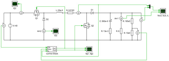
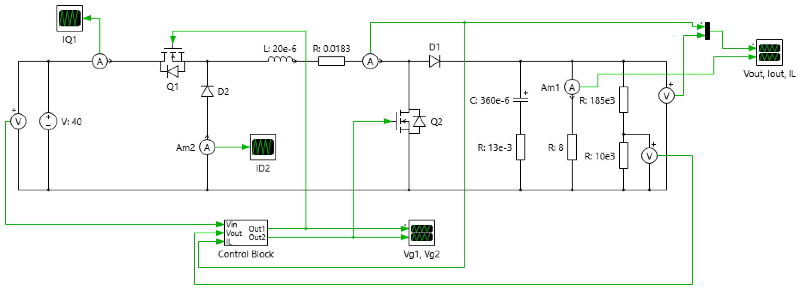
To model the operation of a two-switch buck–boost converter based on the LM5118 in PLECS, it is necessary to develop a behavioral model of the controller that implements its functions. The simulation circuit in PLECS is shown in Figure 3.
Figure 3.
PLECS simulation circuit.
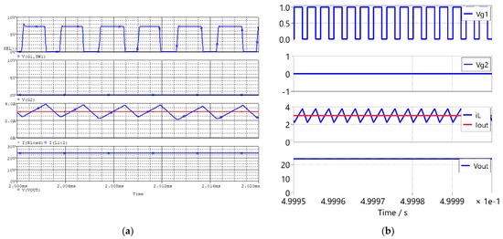
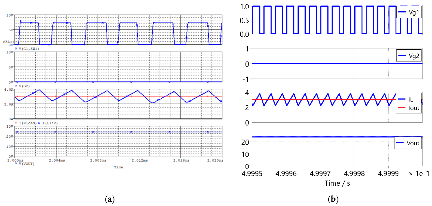
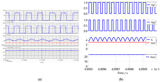
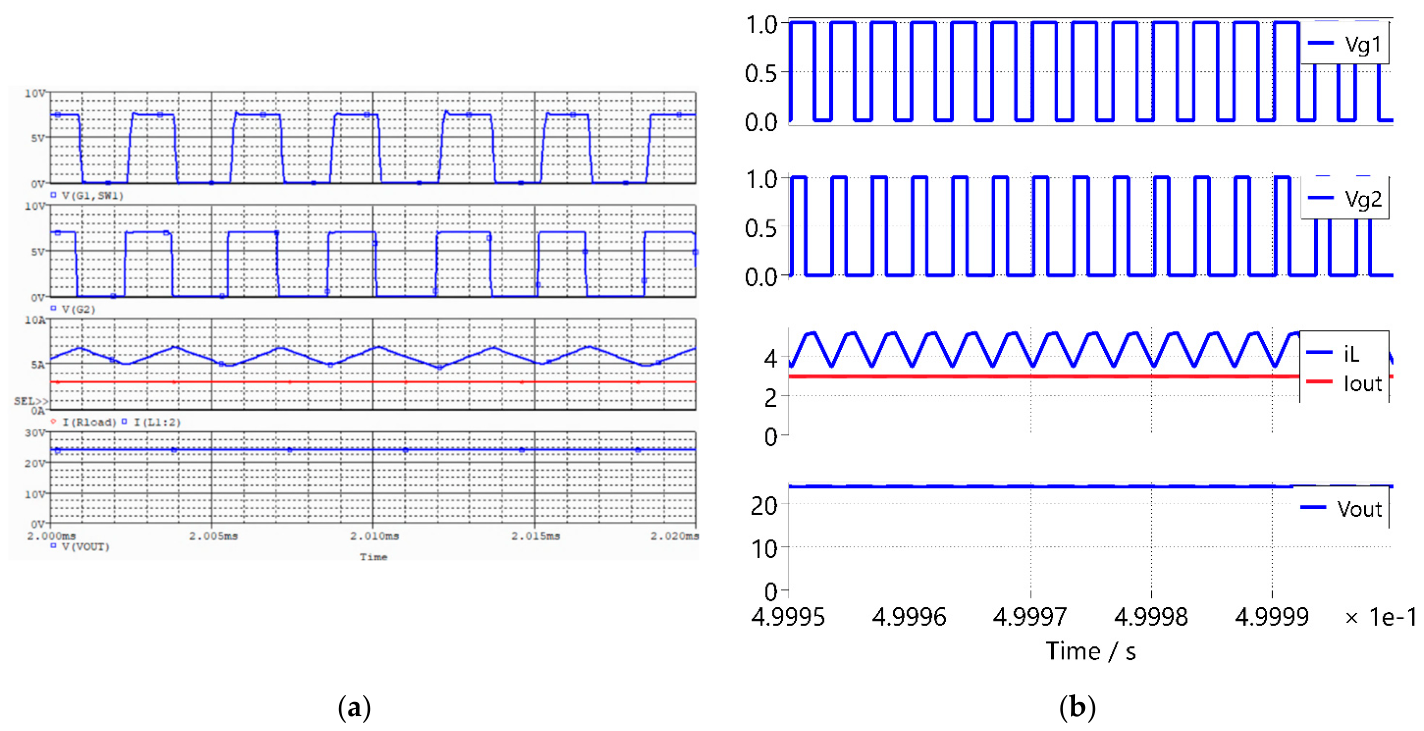
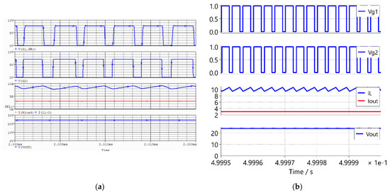
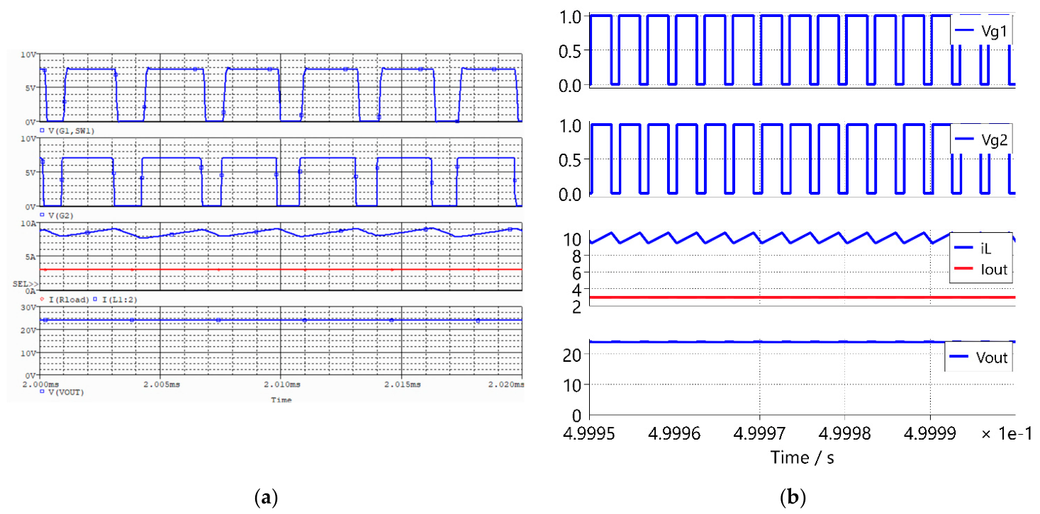
The functions of the LM5118 controller are implemented in the Control Block, and Figure 4, Figure 5 and Figure 6 show the timing diagrams of the control signals obtained from simulations in PSpice for TI and PLECS.
Figure 4.
Buck mode simulation results: (a) PSpice for TI simulation results for VIN = 40 V, VOUT = 24 V, and IOUT = 3 A; (b) PLECS simulation results for VIN = 40 V, VOUT = 24 V, and IOUT = 3 A.
Figure 5.
Smooth transition from buck to buck–boost mode simulation results: (a) PSpice for TI simulation results for VIN = 28 V, VOUT = 24 V, and IOUT = 3 A; (b) PLECS simulation results for VIN = 28 V, VOUT = 24 V, and IOUT = 3 A.
Figure 6.
Simulation results: (a) PSpice for TI simulation results for VIN = 11 V, VOUT = 24 V, and IOUT = 3 A; (b) PLECS simulation results for VIN = 11 V, VOUT = 24 V, and IOUT = 3 A.
Figure 4a presents the PSpice for TI simulation results, and Figure 4b presents the PLECS simulation results for input voltage VIN = 40 V, output voltage VOUT = 24 V and output current IOUT = 3 A as follows: from top to bottom, 1 plot plane—VGS of Q1, 2 plot plane—VGS of Q2, 3 plot plane—current trough inductance L (iL—blue) and output current Iout (red), 4 plot plane—output voltage VOUT.
Figure 5a presents the PSpice for TI simulation results, and Figure 5b presents the PLECS simulation results for input voltage VIN = 28 V, output voltage VOUT = 24 V and output current IOUT = 3 A as follows: from top to bottom, 1 plot plane—VGS of Q1, 2 plot plane—VGS of Q2, 3 plot plane—current trough inductance L (iL—blue) and output current Iout (red), 4 plot plane—output voltage VOUT.
Figure 6a presents the PSpice for TI simulation results, and Figure 6b presents the PLECS simulation results for input voltage VIN = 11 V, output voltage VOUT = 24 V and output current IOUT = 3 A as follows: from top to bottom, 1 plot plane—VGS of Q1, 2 plot plane—VGS of Q2, 3 plot plane—current trough inductance L (iL—blue) and output current Iout (red), 4 plot plane—output voltage VOUT.
The presented results show that the behavioral model accurately describes the control functions of the LM5118 controller.
4.2. Two-Switch Buck–Boost Converter Control-to-Output Transfer Function
To verify the analytical results, PLECS software is utilized to derive the open-loop control-to-output transfer function of the two-switch buck–boost converter.
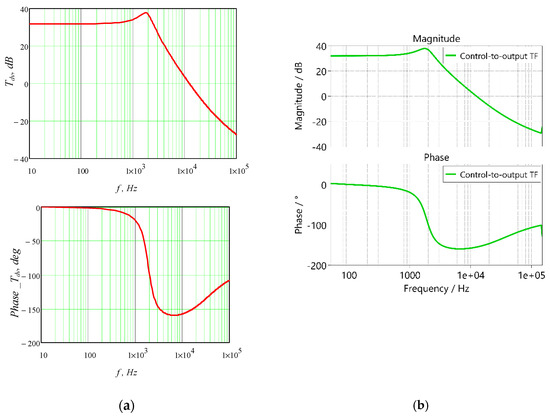
Figure 7a shows buck mode (VIN = 40 V) analytical results for the magnitude dB and the phase response deg of open-loop control-to-output transfer function Tdv(s) according to the given input data. The buck mode PLECS simulation results are plotted in Figure 7b.
Figure 7.
Buck mode AC response of control-to-output transfer function: (a) theoretical control-to-output transfer function Tdvb (s) (VIN = 40 V); (b) PLECS simulation results of control-to-output transfer function Tdvb (s) (VIN = 40 V).
Table 2 presents a comparison of the values of control-to-output transfer function Tdvb (s) obtained from the analytical calculation and from the PLECS simulation.
Table 2.
Comparison of the values of control-to-output transfer function Tdvb (s)—buck mode.
Analyzing the results presented in Table 2, it can be concluded that the relative error between the analytical and PLECS simulation results for the control-to-output transfer function Tdvb(s) is less than 1%.
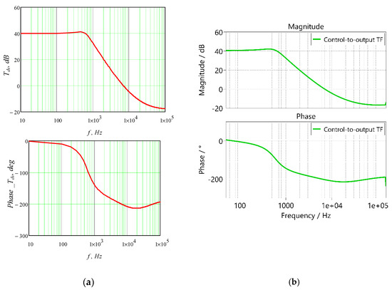
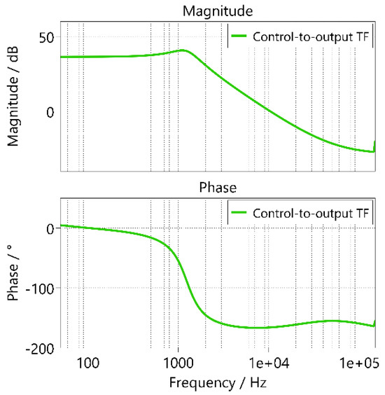
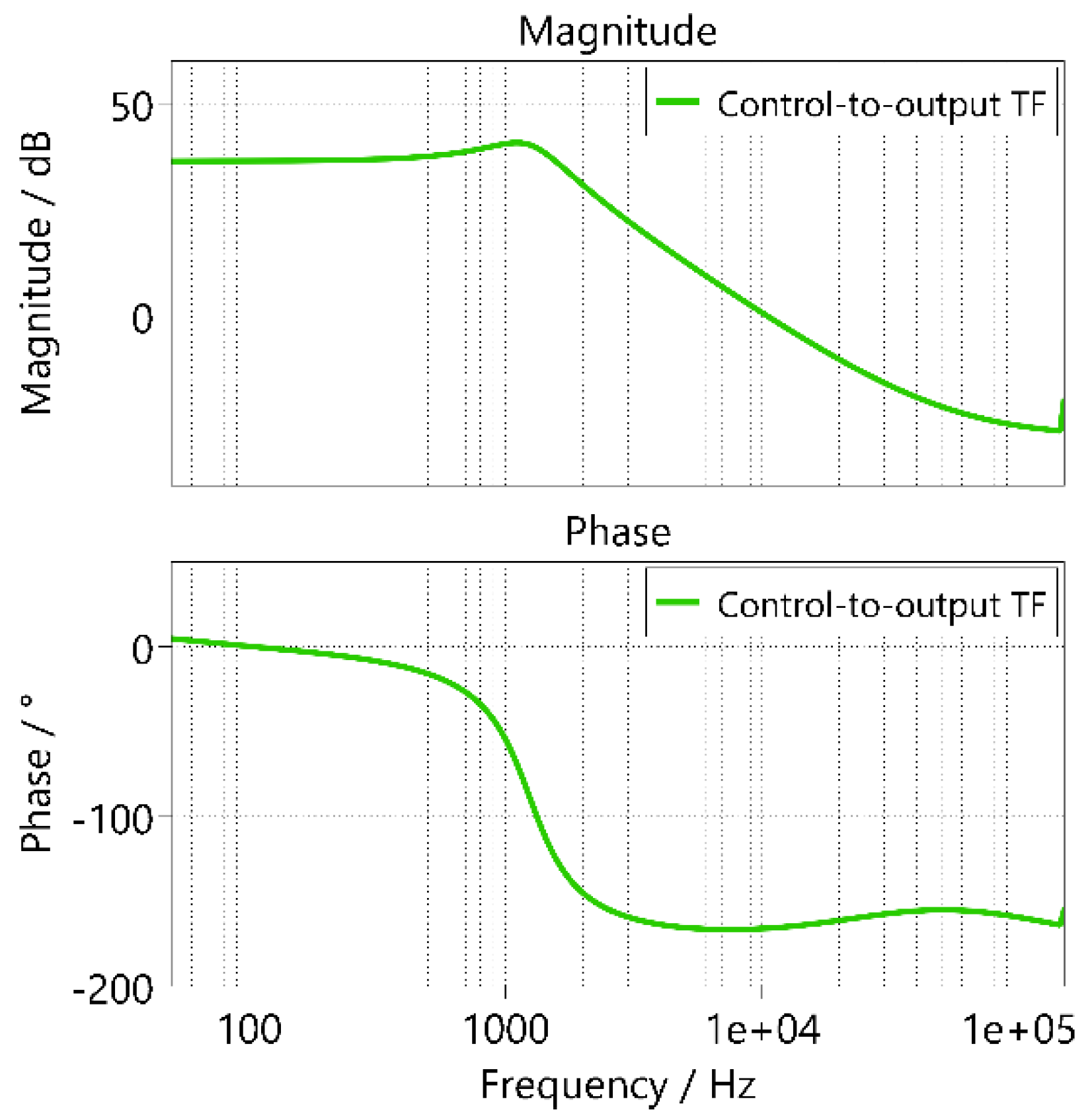
Figure 8a shows buck–boost mode (Vin = 11 V) analytical results for the magnitude dB and the phase response deg of open-loop control-to-output transfer function Tdvbb(s) according to the given input data. Figure 8b shows PLECS simulation results.
Figure 8.
Buck–boost mode AC response of control-to-output transfer function: (a) theoretical control-to-output transfer function Tdvbb (s) (VIN = 11 V); (b) PLECS simulation results of control-to-output transfer function Tdvbb (s) (VIN = 11 V).
Table 3 presents a comparison of the values of control-to-output transfer function Tdvbb (s) obtained from the analytical calculation and from the PLECS simulation.
Table 3.
Comparison of the values of control-to-output transfer function Tdvbb (s)—buck–boost mode.
Analyzing the results presented in Table 3, it can be concluded that the relative error between the analytical and PLECS simulation results for the control-to-output transfer function Tdvb(s) is less than 5%.
Figure 9 shows smooth transition from buck to buck–boost mode (VIN = 28 V) PLECS simulation results for the magnitude dB and the phase response deg of open-loop control-to-output transfer function Tdvbb(s) according to the given input data.
Figure 9.
PLECS simulation results of control-to-output transfer function Tdvbb (s) (VIN = 28 V).
4.3. PSpice Simulation Results
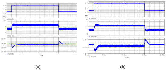
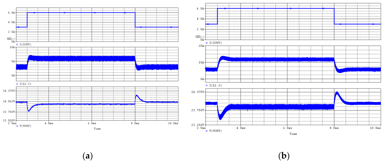
To investigate the dynamic characteristics of the converter circuit, a load change is simulated using an independent current source (IOUT) with a piecewise linear output current waveform—Figure 10. This allows observation of the circuit’s output response during the transition from one steady-state to another with a stepped change in the load current. Up to the time t = 3 ms, the current in the output circuit has a constant value of 3 A, and the converter is in a steady-state mode with RL = 8 Ω. In the time interval from 3 ms to 3.0001 ms (100 ns), a step change in the load current from 3 A to 6 A occurs, i.e., RL = 4 Ω, after which the newly established load current is maintained constant for 5 ms, sufficient for the transient processes to decay and for a new steady-state condition to be established. In the interval from 8 ms to 8.0001 ms (100 ns), a step change in the load current from 6 A to 3 A is applied to investigate the transient processes in the circuit after the initial stimulus has passed. The simulation results of the circuit’s response under the given operating conditions are shown in Figure 11.
Figure 10.
TSBBC PSpice for a TI simulation circuit based on the LM5118 controller for step load changes.
Figure 11.
PSpice simulation results at step load changes: (a) VIN = 40 V, from top to bottom: output current IOUT; current IL through inductance L; output voltage VOUT; (b) VIN = 28 V, from top to bottom: output current IOUT; current IL through inductance L; output voltage VOUT.
It is evident that the LM5118 controller responds to changes, and the circuit stabilizes within ~1 ms during a step increase in the output load (input step) and during a step return to the initial steady-state condition, IOUT = 3 A.
5. Conclusions
This paper presents an in-depth study of the characteristics and behavior of a non-inverting, two-switch buck–boost converter operating in three modes—buck, smooth buck–boost, and buck–boost—determined by the LM5118 controller. Small-signal modeling of the circuit was used to derive an equivalent circuit and determine the control-to-output transfer functions for different operating modes. These functions account for the parasitic elements of the circuit. Additionally, the circuit’s dynamic response was evaluated with a step change in load current from 3 A to 6 A, followed by a return to the initial value. Damped transient processes were observed with a time constant of approximately 1 ms, indicating minimal delay in the circuit’s response.
To study the converter’s characteristics under steady-state conditions and during dynamic processes, we used a simulation model of the LM5118 provided by the manufacturer and analyzed it in the PSpice for TI simulation environment. The analytical relationships derived and assumptions made were confirmed through the design and analysis of a simulation model in the PLECS environment.
Author Contributions
I.I.G. and T.G. were involved in the full process of producing this paper, including conceptualization, methodology, modeling, validation, visualization and preparing the manuscript. All authors have read and agreed to the published version of the manuscript.
Funding
This research was funded by the European Regional Development Fund within the OP “Research, Innovation and Digitalization Programme for Intelligent Transformation 2021–2027”, Project No. BG16RFPR002-1.014-0005 Center of competence “Smart Mechatronic, Eco-, and Energy-Saving Systems and Technologies”.
Institutional Review Board Statement
Not applicable.
Informed Consent Statement
Not applicable.
Data Availability Statement
Data are included in the article.
Acknowledgments
Simulations using PLECS software in this paper were carried out from PLEXIM under the PLECS Academic Sponsorship agreement between the Technical University of Sofia and PLEXIM GmbH.
Conflicts of Interest
The authors declare no conflicts of interest.
References
- Erickson, R.W.; Maksimovic, D. Fundamentals of Power Electronics; Springer: Berlin/Heidelberg, Germany, 2001. [Google Scholar]
- Saha, S.; Mishra, S.; Joshi, A. Multi-Input Bidirectional Resonant Converter for Hybrid Energy Systems. In Proceedings of the IEEE International Conference on Power Electronics, Drives and Energy Systems (PEDES), Jaipur, India, 16–19 December 2020. [Google Scholar] [CrossRef]
- Lichev, A.; Madankov, Y.; Mihov, V.; Spirov, D. Bidirectional Resonant Power Converter for Hybrid Energy Systems. Eng. Proc. 2024, 70, 3. [Google Scholar] [CrossRef]
- Arnaudov, D.; Hinov, N.; Vuchev, S.; Nedyalkov, I. Modeling of Multiphase Converter for Charging of Energy Storage Elements. In Proceedings of the PCIM Europe 2017; International Exhibition and Conference for Power Electronics, Intelligent Motion, Renewable Energy and Energy Management, Nuremberg, Germany, 16–18 May 2017; pp. 1–7. [Google Scholar]
- Nedyalkov, I.; Arnaudov, D.; Hinov, N.; Kanchev, H. Modelling of an off-grid photovoltaic power supplying system for telecommunication equipment. In Proceedings of the 2017 15th International Conference on Electrical Machines, Drives and Power Systems (ELMA), Sofia, Bulgaria, 1–3 June 2017; pp. 64–69. [Google Scholar] [CrossRef]
- Grigorova, T.; Bodurov, G.; Dobrolitsky, M. A Study on a Phase-Shift Controlled ZVS DC-DC Converter with a Synchronous Rectifier. Eng. Proc. 2025, 100, 43. [Google Scholar] [CrossRef]
- Yi, Z.; Zhang, Y.; Wang, X. Review of Voltage Bucking/Boosting Techniques in DC–DC Converters. Energies 2023, 16, 842. [Google Scholar] [CrossRef]
- Kim, S.; Lee, J.; Park, H. Modified Design of Two-Switch Buck-Boost Converter for High Efficiency Applications. Appl. Sci. 2023, 13, 343. [Google Scholar] [CrossRef]
- Jamshidpour, A.; Banaei, M.R.; Khoshkbar-Sadigh, A. Equivalent Two Switches and Single Switch Buck/Buck–Boost Converters for DC Power Supply Applications. Energies 2020, 13, 583. [Google Scholar] [CrossRef]
- Keskin, R.; Aliskan, I. Design of Non-Inverting Buck-Boost Converter for Electronic Ballast Compatible with LED Drivers. Karaelmas Sci. Eng. J. 2018, 8, 473–481. [Google Scholar] [CrossRef]
- Fan, H. Design tips for an efficient non-inverting buck-boost converter. Analog Appl. J. 2014, 31, 20–25. [Google Scholar]
- Analog Devices. Available online: https://www.analog.com/media/en/technical-documentation/data-sheets/ltc3780.pdf (accessed on 10 March 2026).
- Texas Instruments. Available online: https://www.ti.com/lit/ds/symlink/tps63060.pdf (accessed on 10 March 2026).
- Renesas Electronics Corporation. Available online: https://www.renesas.cn/zh/document/dst/isl9110-isl9112-datasheet (accessed on 10 March 2026).
- Texas Instruments. Available online: https://www.ti.com/lit/ds/symlink/lm5118.pdf?ts=1773731220105 (accessed on 15 December 2025).
- Available online: https://www.plexim.com/products/plecs (accessed on 15 December 2025).
- Texas Instruments. Available online: https://www.ti.com/product/LM5118#design-tools-simulation (accessed on 15 December 2025).

Disclaimer/Publisher’s Note: The statements, opinions and data contained in all publications are solely those of the individual author(s) and contributor(s) and not of MDPI and/or the editor(s). MDPI and/or the editor(s) disclaim responsibility for any injury to people or property resulting from any ideas, methods, instructions or products referred to in the content. |
© 2026 by the authors. Licensee MDPI, Basel, Switzerland. This article is an open access article distributed under the terms and conditions of the Creative Commons Attribution (CC BY) license.