


Abstract
In semiconductor manufacturing, automated wafer defect detection is critical for ensuring chip yield and process stability. In seismically active regions, sub-millimeter conveyor micro-displacements during seismic events can produce complex geometric anomalies on wafer surfaces, and the resulting need for rapid post-event inspection motivates the present work. Conventional convolutional neural networks (CNNs) face inherent limitations in capturing global spatial context and suffer from computational redundancy when processing micro-scale, multi-morphological defects. To address these challenges, this study proposes an improved YOLOv11 framework integrating three enhancements: an attention-based intra-scale feature interaction (AIFI) module at the backbone–neck interface to strengthen global semantic correlations, a lightweight asymmetric detection head (LADH) to decouple classification and localization tasks, and a geometry-aware SIoU loss to constrain bounding box regression from angular, distance, and shape perspectives. Experiments on a public benchmark of industrial wafer maps demonstrate that the proposed method improves mAP50 from 93.0% to 94.5% while maintaining 181.7 FPS on a desktop-class GPU. These results demonstrate the effectiveness of the proposed framework for high-throughput wafer-defect inspection on desktop-class hardware, and its low parameter count makes it a promising candidate for future deployment on resource-constrained edge devices.
1. Introduction
The global semiconductor supply chain operates at the frontiers of nanoscale manufacturing precision, where yield enhancement constitutes a decisive competitive differentiator. Wafer fabrication entails a sequence of highly deterministic processes including photolithography, etching, and chemical mechanical planarization, each demanding stringent environmental stability. Given the extraordinarily low fault tolerance inherent to these processes, the entire production ecosystem exhibits pronounced sensitivity to external mechanical disturbances, ranging from low-amplitude micro-vibrations to major seismic events. In semiconductor manufacturing hubs situated along the Pacific Ring of Fire, frequent shallow crustal disruptions pose persistent threats to continuous production operations.
During seismic events and subsequent aftershock sequences, high-speed robotic handlers and automated material handling systems (AMHS) are susceptible to micron-scale trajectory drift and transient mechanical misalignment. Such unintended mechanical perturbations can induce minor physical scratches or edge micro-cracks on wafer surfaces. If these anomalous wafers are not identified and intercepted within the critical post-seismic inspection window, subsequent high-temperature annealing or thin film deposition processes may cause these microscopic defects to propagate into catastrophic wafer breakage or full lot scrappage. Consequently, the establishment of a highly fault-tolerant, automated defect classification and rapid inspection system—capable of operating under such post-seismic conditions—holds substantial industrial value for minimizing production downtime and mitigating economic losses.
Traditional wafer defect detection has long relied on manual optical microscope sampling inspections or automated optical inspection (AOI) systems based on conventional machine vision. Standard AOI algorithms predominantly employ hand-crafted feature engineering, such as Gabor filters, Haar-like features, and support vector machines, in conjunction with template matching paradigms. While such methods exhibit high determinism for defects with fixed shapes and high contrast, their generalization capability degrades significantly when confronted with subtle defects characterized by highly variable morphology, uneven illumination, or low contrast. Moreover, traditional approaches impose stringent requirements on optical focus and mechanical positioning precision, resulting in elevated hardware maintenance costs and limited suitability for real-time dynamic online inspection.
1.1. Research Gap and Motivation
In recent years, deep CNNs have revolutionized the field of industrial defect detection by learning hierarchical feature representations directly from raw images. Among these, the You-Only-Look-Once (YOLO) series of single-stage detectors has been widely adopted in production lines due to its exceptionally high inference throughput. However, the direct transfer of the standard YOLOv11 model to wafer defect detection encounters three persistent bottlenecks:
- (1)
- Spatial semantic dilution: As depth increases, down-sampling layers tend to wash out the edge pixel features of small or faint defects in deeper feature maps. The result is a noticeable drop in localization accuracy for micro-scale anomalies.
- (2)
- Computational redundancy of symmetric detection heads: In the standard detection head, regardless of whether it adopts a coupled or symmetrically decoupled configuration, parameter weights are distributed uniformly across the entire spatial domain. Such indiscriminate allocation leads to substantial computational expenditure on non-defective background regions, thereby adversely affecting the model’s deployability on edge computing platforms.
- (3)
- Lack of geometric constraints in bounding box regression: Existing loss functions, such as CIoU, focus primarily on overlap area and aspect ratio while neglecting the orientation angle of defect bounding boxes. This oversight leads to severe gradient oscillations during training for highly nonlinear scratches with large aspect ratios, resulting in localization drift and compromised regression stability.
Overall, this work addresses three main gaps. Recent YOLO-based detectors for wafer defects [1,2,3] have achieved strong performance, but none specifically targets the micro-scale, high-aspect-ratio geometric anomalies that dominate scratch and edge-crack morphologies, nor the tight time constraints that post-earthquake inspection campaigns would impose. In addition, cross-scale fusion alone does not sufficiently mitigate the spatial semantic dilution of small defect features in deep feature maps. Standard regression losses also lack angular and shape-aware geometric constraints, which leads to unstable localization of elongated scratches. As for the baseline, YOLOv11 was chosen because it offers a favorable trade-off between detection accuracy and inference throughput among open-source single-stage detectors. Its clean architecture, with C3k2 and C2PSA blocks, provides a solid foundation for the targeted enhancements explored here, and it is supported by a mature, actively maintained toolchain.
1.2. Main Contributions
To address the aforementioned technical bottlenecks, this study develops the AIFI-LADH-SIoU multi-mechanism fusion deep learning framework. The principal contributions of this work are threefold:
- (1)
- Synergistic optimization through multi-mechanism fusion architecture: Building upon the YOLOv11 baseline, this study systematically integrates the AIFI module, the LADH detection head, and the SIoU loss function through a structured architectural design. This integration achieves a dynamic balance between detection precision and inference speed, effectively reconciling the conflicting demands of accuracy and computational efficiency in industrial inspection scenarios.
- (2)
- Mechanism-driven ablation studies with quantitative rigor: Through carefully controlled experiments, this work quantitatively dissects the individual mathematical contributions of single-scale feature interaction and asymmetric gradient decoupling to the model’s generalization capacity. The resulting analysis provides theoretical substantiation for architectural optimization in industrial defect detection models, offering insights that extend beyond the specific framework proposed herein.
- (3)
- Benchmark-based validation under time-critical inspection requirements: The proposed framework is evaluated on a public wafer-defect benchmark covering a wide range of wafer surface anomalies. Experimental results demonstrate that the framework effectively adapts to the feature extraction challenges posed by high-aspect-ratio scratches and edge micro-cracks, meeting the accuracy and speed requirements of real-time production line environments.
1.3. Organization
The remainder of this paper is organized as follows. Section 2 reviews the evolution of semiconductor wafer defect detection technologies and the progression of related deep learning methods. Section 3 details the proposed AIFI-LADH-SIoU framework, including the overall architecture and the specific design of each of the three components. Section 4 describes the experimental setup and dataset, the comparative analyses of attention mechanisms, detection heads, and loss functions, the ablation study, the model complexity analysis, and the visualization analysis. Section 5 concludes the paper and outlines directions for future research.
2. Related Work
In semiconductor wafer manufacturing, the detection and analysis of chip surface defects constitute a pivotal link in ensuring product yield and reliability. External environmental disturbances, particularly seismic events, can induce multifaceted impacts on the fabs, affecting equipment, materials, and ambient conditions, thereby generating diverse surface damage on wafers [4]. In such scenarios, engineers typically commence with defect distribution maps, systematically analyzing defect patterns and types in conjunction with inspection data. Fabs are equipped with an array of high-precision analytical instruments, forming a comprehensive quality monitoring and failure analysis framework.
Conventional wafer defect detection, being time-consuming and labor-intensive, has become inadequate to meet contemporary demands. With the advent of artificial intelligence, Cheon et al. [5] proposed CNN-based approaches, and Shinde et al. [6] introduced YOLO-based deep learning algorithms, both of which have been widely adopted for automated image recognition of defect distribution maps. By training on extensive defect samples, these systems can rapidly and accurately identify and classify various surface damage categories. When combined with chip distribution maps for defect statistics and trend analysis, such systems can serve as a valuable decision support tool for reducing product scrappage along production lines. In the aftermath of seismic events, the timely and comprehensive detection of defects induced by equipment displacement not only enhances throughput but also constitutes a critical safeguard for rapid production recovery.
2.1. Evolution of Semiconductor Wafer Defect Detection Technologies
Over the past decades, driven by escalating global chip demand and the imperative to sustain quality and yield, wafer defect detection has progressively transitioned from manual inspection to automated image processing solutions [7]. Wafer defect detection methodologies can be broadly categorized into automated visual inspection systems and electron-beam inspection systems [8]. Automated visual inspection employs high-resolution cameras and image processing techniques for non-contact inspection, while electron-beam inspection systems scan sample surfaces to acquire high-resolution images through secondary electron signals.
Automated visual image processing, grounded in computer vision and deep learning, aims primarily at achieving rapid, precise, and quantifiable defect identification and classification. To realize automated wafer defect detection, numerous scholars have proposed diverse solutions. Wang et al. [9] and Yuan et al. [10] developed statistical methods employing distinct probabilistic models to discriminate defect patterns. Chang et al. [11] introduced unsupervised self-organizing neural networks for automatic feature learning and recognition. Yuan et al. [12] further proposed a redetection method combining correlation filters and particle filtering from a visual tracking perspective. Collectively, these studies have established a multifaceted technical foundation for intelligent wafer defect identification.
To improve yield and equipment monitoring, wafer defect detection has shifted from simple pass or fail classification to detailed defect typing and accurate positioning. This shift supports prompt equipment shutdown for maintenance and early detection of anomalies. In response to this demand, numerous automated classification methods have been proposed: Wang [13] employed spectral clustering for defect pattern recognition; Wu et al. [14] proposed failure pattern identification and feature similarity ranking for large-scale datasets; Bourgeat et al. [15] combined Gabor filters with Support Vector Machines (SVM) for feature extraction and classification; Fan et al. [16] developed optical-based multi-label classification methods; and Baly et al. [17] implemented SVM for wafer feature classification. These approaches have collectively propelled defect detection toward greater intelligence and granularity.
While the methods discussed above have made meaningful contributions to wafer defect detection and classification, they share a common limitation. They depend on near-perfect alignment between target and template images, which imposes highly demanding requirements on classification precision. To meet this standard, most fabs still rely on conventional approaches that use complex and costly built-in hardware for defect classification and localization. This practice inevitably increases production costs. Moreover, in emergency situations such as post-earthquake large-scale inspections, these methods often struggle to maintain accuracy. This seriously undermines detection reliability and slows down subsequent responses. Therefore, developing a high-precision yet cost-effective wafer defect classification technique has become an urgent and critical challenge.
2.2. Technological Progression in Wafer Defect Detection
As chip fabrication processes grow increasingly complex, a single wafer surface may exhibit diverse defect morphologies across multiple process steps, motivating the development of coordinate-based segmentation and annotation techniques for distinct regions. Chen et al. [18] proposed a high-tolerance, robust segmentation method for defect regions in randomly textured backgrounds, with approaches broadly classified into learning-based and feature-matching-based categories. Within the learning paradigm, Chen et al. [19] employed Atrous Spatial Pyramid Pooling for robust multi-scale object segmentation. Long et al. [20] adapted classification networks, including AlexNet, VGG, and GoogLeNet, into fully convolutional networks, fine-tuning their feature representations for segmentation tasks. Chiu et al. [21] and Wang et al. [22] applied Mask R-CNN segmentation models to wafer map defect detection, achieving precise identification and localization of various defect types through optimized network architectures and training strategies. Although learning-based methods demonstrate superior segmentation performance, they typically require substantial labeled samples for training and exhibit limited adaptability to continuously evolving wafer patterns in practical contexts. Under the constraints of limited samples and variable patterns characteristic of semiconductor manufacturing environments, Bourgeat et al. [23] proposed a segmentation algorithm tailored for semiconductor wafer images generated by optical inspection tools. Zhen et al. [24] developed a machine vision-based wafer defect detection and classification system. Huang et al. [25] introduced a binary segmentation method for centerline localization in wafer images.
With rapid advances in industrial imaging and deep learning, vision-based wafer defect detection has achieved remarkable precision and efficiency, establishing deep learning as a cornerstone of intelligent manufacturing research. Piao et al. [26] employed Radon transform feature aggregation with decision trees, achieving 90.5% accuracy through multi-angle projection for enhanced geometric description. In the supervised learning domain, Behera et al. [27] optimized SVM parameters to facilitate classification, attaining 88.1% accuracy. Dash et al. [28] combined hybrid feature selection with hyperparameter-tuned gradient boosting, achieving 74.5% accuracy.
More recently, YOLO-based detectors have been increasingly applied to wafer surface defect detection, and they currently represent the state of the art in this field. Zhu et al. [1] proposed SGW-YOLOv8, which integrates the SimAM attention mechanism, a GhostConv backbone, and the WIoU loss, improving mAP@0.5 by 4.8% over the YOLOv8 baseline while reducing the number of parameters by 11.8%. Xu et al. [2] developed RFS-YOLOv8n, which combines RepViT blocks, context-anchor attention, a feature-focused diffusion pyramid neck, and a shared lightweight detection head, reaching an mAP50 of 98.2% with 34.7% fewer parameters. Chi et al. [3] presented CISC-YOLO, a lightweight network with efficient cross-scale feature fusion that attains an mAP50 of 93.7% with only 1.92 M parameters. These studies indicate that current research efforts focus on balancing detection accuracy, model size, and inference speed; however, none of them specifically addresses the detection of high-aspect-ratio geometric anomalies under the time constraints of large-scale post-earthquake inspection, which constitutes the application niche targeted by the present study.
Given these considerations, the selection of an appropriate wafer defect detection approach has become an urgent priority. Historically, artificial intelligence-based computer vision recognition incurred substantial software and hardware costs. However, recent years have witnessed rapid advancements in AI and computer vision software [29], accompanied by continuous innovation in graphics processing hardware. Following comprehensive evaluation and literature review, this study adopts artificial intelligence as its foundational framework, with particular emphasis on the YOLO model. YOLO has maintained widespread influence across diverse domains for over a decade in real-time object detection [30]; being open source, it also offers the flexibility needed to optimize the model toward the specific characteristics of wafer defects. It is, therefore, adopted as the core architecture for computer-vision-based wafer defect detection in this study.
Two-stage detectors (e.g., the R-CNN series) offer high accuracy but are too slow for time-critical, data-scarce inspection scenarios such as post-earthquake assessment, whereas single-stage YOLO detectors meet the real-time requirement. Within the YOLO family, YOLOv11 was chosen because its C2PSA module explicitly targets small, low-contrast objects—precisely the characteristics of wafer defects—and recent wafer-defect studies [1,2,3] build on the same generation.
3. Methodology
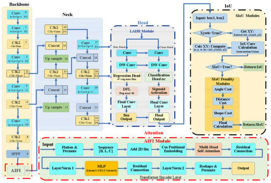
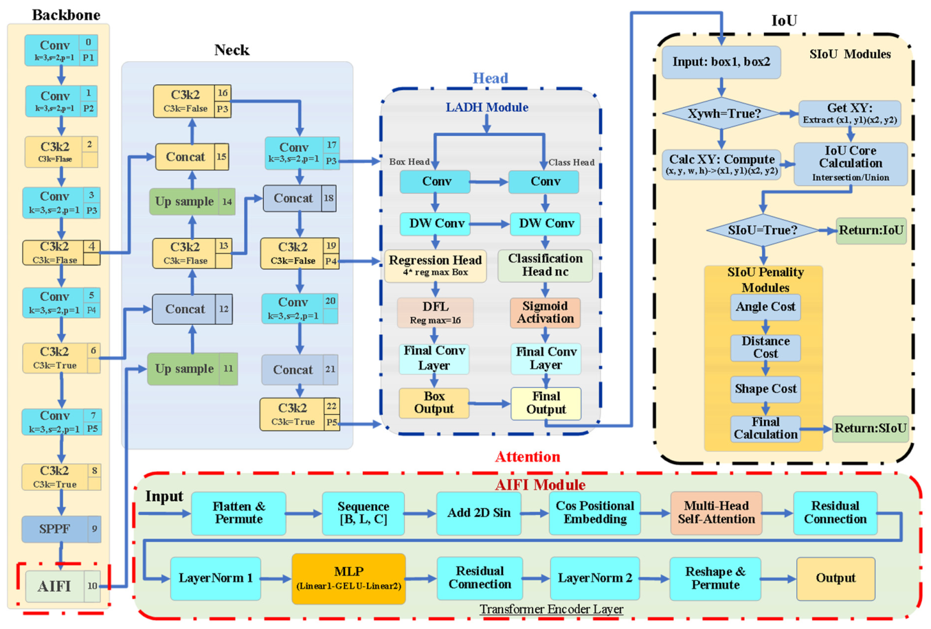
This section presents the proposed AIFI-LADH-SIoU YOLO framework, a structured enhancement of the YOLOv11 architecture specifically designed for wafer surface defect detection. The methodology focuses on three critical aspects of the object detection pipeline: attention-based feature interaction, detection head architecture, and loss function design. Each component is systematically optimized to address the unique challenges posed by microscale, morphologically diverse wafer defects, including spatial semantic dilution, computational redundancy, and insufficient geometric constraints in bounding box regression. Figure 1 illustrates the overall network architecture of the proposed AIFI-LADH-SIoU YOLO model.
Figure 1.
The overall network architecture of the proposed AIFI-LADH-SIoU YOLO model.
3.1. Overall Architecture
Building upon the YOLOv11 baseline, the proposed AIFI-LADH-SIoU YOLO framework integrates three key components—each building on well-established techniques from prior work and jointly tailored to wafer defect detection—into a cohesive detection pipeline:
- (1)
- AIFI module [31]: Positioned at the backbone–neck interface and applied to the highest-level (P5) feature map immediately after SPPF, this module enhances global contextual reasoning across high-level semantic features, mitigating the spatial dilution problem inherent in deep CNNs.
- (2)
- LADH: Adapted from the lightweight asymmetric detection head originally proposed by Zhang et al. [32] to replace the standard detection head, this design decouples classification and localization tasks while significantly reducing parameter count, which is expected to improve inference efficiency on resource-constrained platforms.
- (3)
- SIoU loss: Proposed by Gevorgyan [33] and adopted here as the bounding box regression loss, this function incorporates geometric constraints—including angle, distance, and shape—to stabilize training and improve localization accuracy for high aspect ratio defects such as scratches.
The following subsections detail each of these components.
3.2. AIFI Module: Attention-Based Intra-Scale Feature Interaction
Traditional multiscale feature fusion networks, such as PANet or FPN, mitigate the challenge of object scale variation through cross-scale feature propagation. However, when processing deep feature maps—such as the P5 layer—repeated nonlinear convolutions and cross-scale interpolation operations tend to introduce substantial high-frequency noise, thereby blurring the geometric edges of microscale defects.
To address this issue, the present study adapts the AIFI module—originally proposed as a core component of the RT-DETR hybrid encoder [31]—and inserts it into the highest-level (P5) feature map immediately after SPPF, at the junction between the backbone and the neck. Unlike conventional attention mechanisms, AIFI restricts feature interaction strictly within the same scale, deliberately avoiding cross-scale nonlinear convolutions. By performing self-attention computation exclusively on a single scale, the network is able to capture global spatial long-range dependencies across the entire image:
where the query matrix (Q), key matrix (K), and value matrix (V) are all derived from the identical single-scale feature tensor X ∈ RH×W×C. This design effectively eliminates the semantic interference introduced by cross-scale fusion while preserving global spatial coherence. Consequently, the model maintains the capability to recognize discontinuous fragments of elongated scratches as a single continuous geometric entity, even when such defects appear as interrupted line segments across the image.
It should be clarified that the intra-scale interaction of AIFI and the multiscale fusion of the neck are complementary rather than contradictory: AIFI performs self-attention only on the highest-level semantic feature (the P5 map), after which its output is combined with lower-level features through the conventional PAN/FPN-style cross-scale fusion of the neck. In other words, intra-scale interaction strengthens the semantic representation of the deepest features before cross-scale fusion takes place, while the overall network remains a multiscale fusion pipeline.
3.3. LADH: Lightweight Asymmetric Detection Head
In mainstream object detectors, classification and regression typically share the same network pathway or employ a symmetrically decoupled structure. However, these two tasks are inherently contradictory in their optimization objectives: classification requires translation-invariant, high-level semantic abstraction, whereas regression demands translation-covariant, precise spatial positional information.
The LADH structure, originally proposed by Zhang et al. [32] and adapted in this study for wafer defect detection, introduces an asymmetric parameter allocation mechanism. Given that precise geometric localization of micro-scale defects requires stronger spatial representation capability, LADH assigns a higher computational weight to the regression branch, employing depth-wise separable convolutions in conjunction with asymmetric multilevel convolutional kernel compression. Meanwhile, the classification branch undergoes substantial lightweight pruning to prevent redundant parameters from inducing overfitting:
where Wdw denotes the depth-wise convolution operator, and Wpw denotes the pointwise convolution operator. Through asymmetric gradient decoupling, the model substantially reduces floating-point operations (FLOPs) while improving bounding box convergence accuracy, which indicates its suitability for future deployment on resource-constrained edge platforms.
Outputreg = Fasym(Wdw ∗ X), Outputcls = Flight(Wpw ∗ X)
3.4. SIoU Loss: Shape-Aware Bounding Box Regression
Traditional bounding box regression loss functions, such as CIoU, primarily consider the center point distance and aspect ratio between the predicted box and the ground truth box during optimization. However, in the early stages of training, if an arbitrary angular offset exists between the predicted and ground truth boxes, the gradient direction of the center point connection line exhibits severe directional uncertainty, causing the predicted box to wander randomly in the spatial domain.
To render the optimization path of the bounding box maximally deterministic, this study adopts the SIoU loss function proposed by Gevorgyan [33], which constructs a three-tier geometric constraint system encompassing angle, distance, and shape. The optimization process first employs an angle cost (Λangle) to forcibly align the center point connection line between the predicted and ground-truth boxes to the nearest coordinate axis:
Once the angular adjustment stabilizes, the distance cost (Λdistance) incorporates the angle optimization coefficient to dynamically penalize the relative displacement between the two center points along the coordinate axes:
Finally, the shape cost (Λshape) imposes exponential geometric similarity constraints on the aspect ratio discrepancies between the two boxes:
By fusing angle, distance, and shape into a unified optimization scalar, SIoU explicitly constrains the degrees of freedom in bounding box regression, achieving exceptionally high convergence speed and localization precision.
For completeness, the overall SIoU regression loss employed in this work is expressed as
where the angle cost is implicitly incorporated into the distance cost through the coefficient γ = 2 − Λangle.
4. Experiment Description and Result Analysis
To validate the efficacy of the proposed AIFI-LADH-SIoU framework, all experiments were conducted on a workstation whose hardware configuration comprised an Intel Core i9 central processing unit, 64 GB of system memory, and a single NVIDIA GeForce RTX 4090 graphics accelerator with 24 GB of VRAM. The operating system was Linux Ubuntu 22.04, and the development environment was built upon PyTorch 2.1 with CUDA 12.1.
The experimental dataset encompasses a comprehensive range of common defects encountered in real-world wafer fabrication processes, including surface line scratches, edge cracks, point defects, and other typical anomalies. All input images were uniformly resized to a standardized resolution of 640 × 640 pixels. The model was trained for a total of 300 epochs, employing the Stochastic Gradient Descent (SGD) optimizer with an initial learning rate of 0.01 and a momentum factor of 0.937. The batch size was set to 16 for all training sessions. The baseline detector used in all experiments is the YOLOv11-n scale variant.
4.1. Dataset Description
All images were drawn from the publicly available MIR-WM811K wafer-map dataset released by the Mixed-Signal R&D Laboratory (MIRLab), National Chi Nan University, Taiwan, China [14], which is accessible at https://www.kaggle.com/datasets/qingyi/wm811k-wafer-map (accessed on 9 October 2026). This dataset is a widely used benchmark whose images are wafer-map renderings exported from in-line inspection and yield-management systems. An initial pool of more than 16,000 images was retrieved; since many proved blurred, defect-free, or near-duplicated, the pool was screened manually against three criteria—image clarity, defect visibility, and redundancy—leaving 9000 high-quality samples. These images constitute a general-purpose public benchmark and are not accompanied by seismic-event metadata; the experiments reported in this work therefore characterize detection accuracy and inference throughput on representative wafer-defect morphologies that serve as a proxy for the conditions a post-seismic inspection campaign would impose, rather than defects verified to have originated from seismic events.
To keep the evaluation protocol rigorous, the 9000 retained images were first partitioned at the source-image level into mutually exclusive training, validation, and test subsets in a 70/20/10 ratio (6300/1800/900 images). Offline augmentation—rotations of 90°, 180°, and 270°, together with a mosaic operation merging four images into a single composite—was applied afterwards and exclusively to the training subset; the outputs were inspected visually to confirm that no geometric distortion had been introduced. This added 3857 samples and brought the training set to 10,157 images (12,857 in total). Because the validation and test subsets were separated before any augmentation was carried out, they contain only original, non-augmented wafer maps, and no augmented variant of an evaluation image occurs anywhere in the dataset; the metrics reported below therefore rest on data strictly independent of the training set. All images were uniformly resized to 640 × 640 pixels at the network input, and the same partition was used by every model configuration compared in this study.
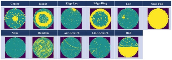
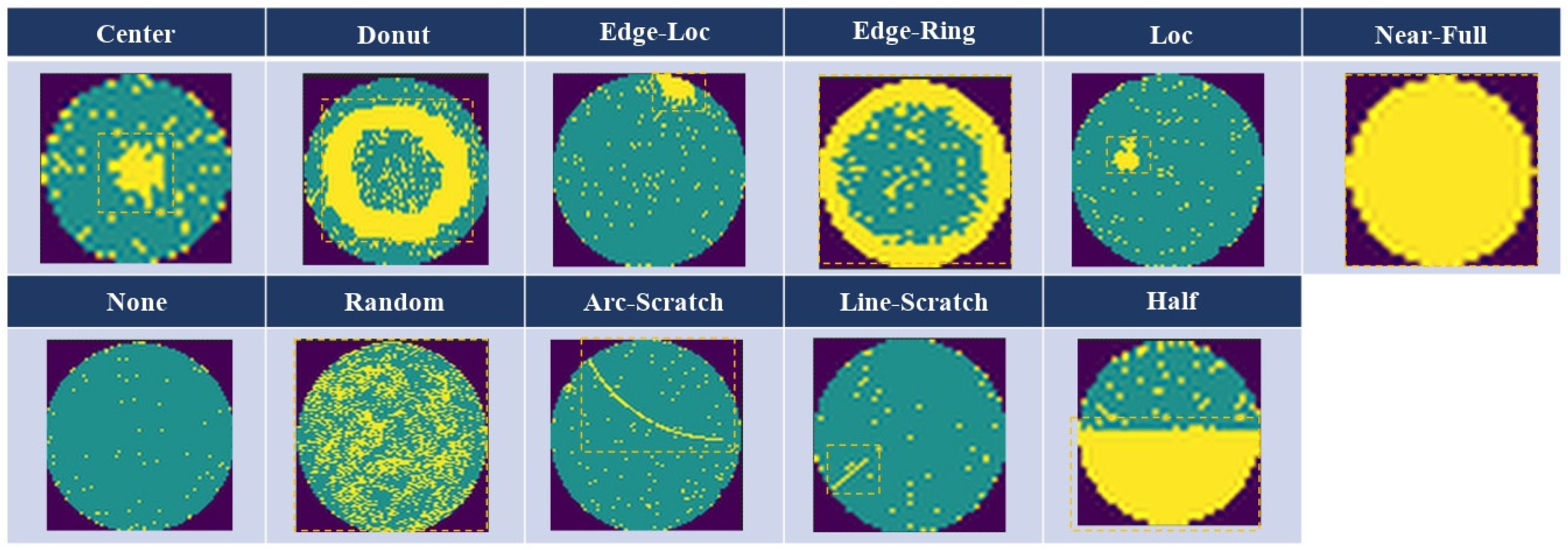
The dataset covers eleven defect categories: Center, Donut, Edge-Loc, Edge-Ring, Loc, Near-Full, None, Random, Arc-Scratch, Line-Scratch, and Half. Edge-Loc is by far the most frequent, comprising 10,695 annotated objects across 5675 images and accounting for roughly 42% of all annotations; Line-Scratch follows with 3495 objects in 2240 images, and Edge-Ring with 2615 objects in 2590 images. Center (2545 objects in 2430 images), Loc (2325 in 1845), None (1040 in 1040), Random (790 in 785), Arc-Scratch (755 in 535), and Donut (675 in 670) occupy the intermediate range, whereas Near-Full (255 objects) and Half (75 objects) are rare, together representing less than 1.5% of the annotations. In total, the dataset contains 25,265 annotated objects; since a single wafer map may carry more than one defect type, the per-class image counts sum to a value larger than the number of images. Representative samples of all eleven categories are shown in Figure 2.
Figure 2.
Representative wafer-map samples of the eleven defect categories in the dataset.
Of the eleven categories, the two scratch types warrant particular attention. Unlike the regional patterns, which are tied to a specific zone of the wafer, Arc-Scratch and Line-Scratch are elongated, high-aspect-ratio anomalies that frequently run nearly parallel to the surrounding die texture. Such thin, low-contrast targets are readily confused with the periodic lattice of the wafer map, which is why Line-Scratch remains the weakest category in the per-class Precision–Recall analysis and constitutes a central motivation for the present framework.
Annotation was performed manually with a YOLO-compatible graphical labeling tool: each defect region was enclosed in a bounding box and assigned one of the eleven class labels, and every image was exported as a JPG file paired with a plain-text annotation in the standard YOLO format (class index plus normalized box coordinates). The labeled data were organized in a unified directory structure and a data.yaml file specifying the subset paths and class names was created to drive the Ultralytics training pipeline.
4.2. Comparative Analysis of Attention Mechanisms
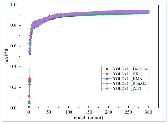
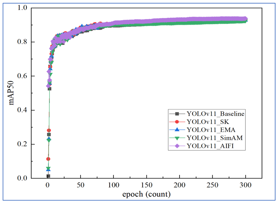
To systematically evaluate the impact of different attention mechanisms on wafer defect detection performance, this study conducted a comprehensive comparative analysis of four representative attention modules: SK, EMA, SimAM, and the AIFI module (adapted from [31]). Through a carefully designed experimental protocol, each mechanism was assessed in terms of feature extraction capability, computational efficiency, and detection accuracy. The objective was to identify the most effective attention strategy for enhancing multi-scale defect perception and localization precision in wafer inspection tasks. The quantitative comparison results are presented in Figure 3 and summarized in Table 1.
Figure 3.
Comparison of mAP50 performance between YOLOv11 and different attention mechanisms.
Table 1.
Performance comparison of different attention mechanisms integrated into the YOLOv11 baseline model.
Among the four attention modules evaluated, the AIFI module consistently outperformed its counterparts across most key metrics, achieving the highest Precision (0.892), mAP50 (93.7%), and mAP50–95 (86.5%). Although SK demonstrated a slight advantage in Recall (0.866), its overall mAP50 declined to 92.8%, primarily due to excessive background texture noise introduced by dynamic multi-scale kernel operations. In contrast, AIFI’s single-scale intra-feature interaction mechanism effectively suppresses false positives while preserving fine-grained defect characteristics, significantly reducing miss-detection rates for microscale anomalies. These results confirm that AIFI’s single-scale intra-feature interaction mechanism is particularly well suited for capturing subtle wafer defect features, thereby validating its integration into the proposed detection framework.
4.3. Comparative Analysis of Detection Heads
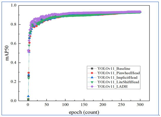
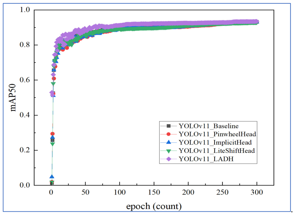
The detection head is the second design variable. Four representative architectures—Lite Shift Head, Pinwheel Head, Implicit Head, and the LADH—were trained and evaluated under the same conditions and metrics as in Section 4.2, namely Precision, Recall, mAP50, mAP50–95, and inference speed (FPS). Figure 4 presents the mAP50 comparison, and Table 2 summarizes the full results.
Figure 4.
Comparison of mAP50 performance between YOLOv11 and different detection heads.
Table 2.
Performance comparison of different detection heads integrated into the YOLOv11 model.
As evidenced by the experimental results, the LADH demonstrates superior overall performance across the majority of evaluation metrics. A detailed analysis of the four detection heads reveals the following observations:
Precision: LADH achieves the highest Precision of 0.881, indicating its distinct advantage in accurately identifying true defect instances while minimizing false positives in wafer surface inspection.
Recall: Pinwheel Head attains the highest Recall of 0.871, suggesting its effectiveness in capturing a broader range of defect samples, albeit at the expense of increased false detections.
mAP50: LADH achieves the highest mAP50 of 93.4%, demonstrating its strong detection capability for easily identifiable chip surface damage targets.
mAP50–95: LADH and Implicit Head achieve comparable performance at 86.0% and 85.7%, respectively, indicating that both architectures maintain robust detection accuracy under stringent IoU thresholds.
Overall, the LADH’s asymmetric parameter allocation and depth-wise separable convolution design effectively capture subtle defect features while significantly reducing both false positives and miss-detections. These results validate the architectural advantages of the proposed lightweight asymmetric detection head for semiconductor wafer inspection tasks.
4.4. Comparative Analysis of Loss Functions
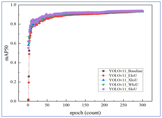
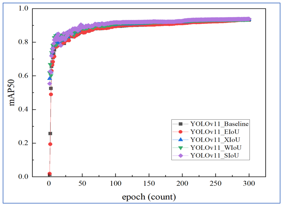
Finally, the bounding box regression loss was examined with the architecture held fixed so that any performance difference can be attributed to the loss alone. Four IoU-based losses—EIoU, SIoU, XIoU, and WIoU—were compared on the same metrics as before. Table 3 lists the results, and Figure 5 visualizes the mAP50 comparison.
Table 3.
Performance comparison of different IoU loss functions integrated into the YOLOv11 model.
Figure 5.
Comparison of mAP50 performance between YOLOv11 and different loss functions.
A comprehensive analysis of the four loss functions reveals distinct performance characteristics:
SIoU achieves the highest Precision (0.888), mAP50 (93.7%), and mAP50–95 (86.6%, as listed in Table 3), demonstrating superior overall detection capability. While its Recall (0.860) is slightly lower than EIoU’s peak value, the balanced performance across all metrics positions SIoU as the most robust choice for wafer defect detection.
XIoU delivers competitive performance with Precision of 0.885, Recall of 0.856, and an mAP50 of 93.4%. The introduction of center point distance penalization effectively reduces center offset; however, its fine-tuning capability for microscale defect bounding boxes remains marginally inferior to SIoU.
EIoU achieves the highest Recall (0.867) among all configurations, likely attributable to its dynamic weighting mechanism that adapts to sample imbalance and reduces suppression effects. However, this comes at the cost of the lowest Precision (0.865); its mAP50–95 (86.3%) also falls slightly below that of SIoU.
Inference Speed Analysis: Using the RTX 4090 as the inference-speed test platform (all FPS values reported in this paper were measured on this GPU; see the hardware clarification at the beginning of Section 4), the FPS values for the four loss functions are as follows: EIoU (195.3), SIoU (197.0), WIoU (195.6), and XIoU (193.0). Since IoU losses are applied exclusively during the training phase without modifying the inference architecture, the observed speed variations—remaining within a marginal fluctuation of approximately 4%—are attributable to measurement noise and batching effects rather than to any architectural difference. These differences are negligible for real-time detection applications.
Comprehensive Evaluation: Considering both accuracy and efficiency, SIoU achieves the best overall balance among the evaluation metrics while maintaining a competitive inference speed of 197.0 FPS that is comparable to the baseline (201.2 FPS), demonstrating the best Precision–speed trade-off among the four loss functions evaluated; it is noted that its Recall (0.860) is slightly lower than that of EIoU (0.867). These results substantiate the integration of SIoU into the proposed AIFI-LADH-SIoU framework for wafer defect detection tasks.
4.5. Model Complexity and Efficiency Analysis
Beyond detection accuracy, the practical value of an inspection model on a production line depends heavily on its computational footprint. This subsection therefore examines the proposed framework from the perspective of model complexity and runtime efficiency. The parameter counts, GFLOPs, and inference speeds reported below were taken directly from the fused model summaries and per-image timing outputs of the experiments described in Section 4.2, Section 4.3 and Section 4.4, with all timing measurements performed on the same machine. Table 4 summarizes the results alongside the baseline.
Table 4.
Model complexity and inference efficiency of the baseline and the proposed components.
4.6. Ablation Study and Module Contribution Analysis
To further deconstruct the complementary synergistic effects among the AIFI module, the LADH detection head, and the SIoU loss function, a systematic multistage ablation study was conducted. Detailed experimental results are recorded in Table 5.
Table 5.
Ablation experiment results of the AIFI-LADH-SIoU multi-mechanism fusion optimization pathway.
The ablation data reveal several important insights regarding the architectural optimization mechanism:
- (1)
- Individual component contributions: When the AIFI module was introduced in isolation (No. 2), mAP50 improved from 93.0% to 93.7%, representing a net gain of 0.7 percentage points. This confirms that the single-scale intra-feature interaction mechanism effectively enhances global contextual reasoning and mitigates the spatial dilution of micro-defect features. The LADH detection head alone (No. 3) elevated mAP50 to 93.4%, demonstrating that parameter decoupling between classification and regression branches significantly alleviates gradient optimization conflicts between the two tasks. Notably, when SIoU was adopted as the sole modification (No. 4), mAP50 increased to 93.7% without any additional inference overhead, maintaining a high FPS of 197.0. This confirms that the shape-aware geometric constraint offers a “performance improvement without cost” advantage.
- (2)
- Full integration synergy: When all three modules were jointly incorporated into the AIFI-LADH-SIoU configuration (No. 8), the model achieved its peak performance, with mAP50 reaching 94.5% and mAP50–95 attaining 87.3%—representing a substantial improvement of 1.5 and 2.2 percentage points over the baseline, respectively. While the dense feature interactions and asymmetric pathways caused a moderate reduction in inference speed to 181.7 FPS, this frame rate remains significantly higher than the typical industrial requirement for real-time inline inspection (30–60 FPS). Thus, the proposed framework successfully achieves an optimal balance between ultra-high precision and practical real-time deployability.
4.7. Visualization Analysis and Local Confidence Quantitative Evaluation
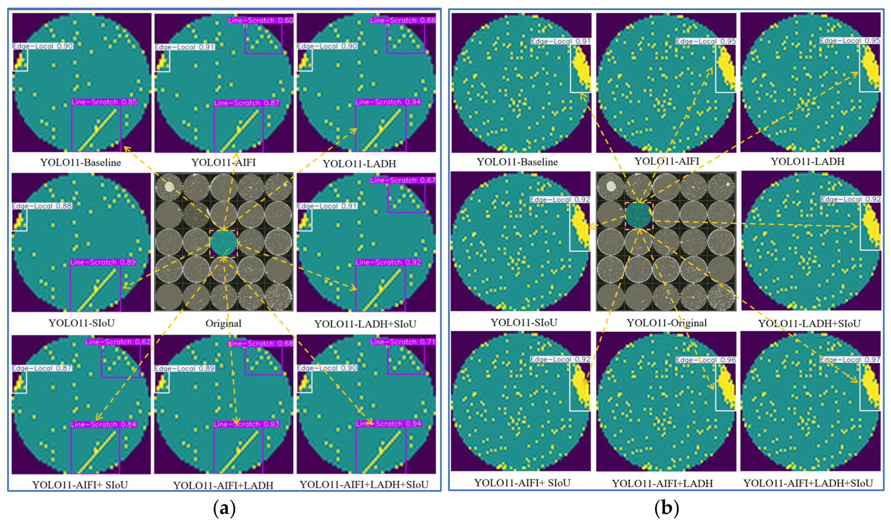
To intuitively evaluate the model’s localization capability on actual wafer edge regions or complex surface nonlinear defects, this study performed a comparative visualization of feature maps and detection bounding boxes on severe scratch samples. Under the baseline YOLOv11 model, the confidence score for the predicted bounding boxes was merely 0.85, as scratch edge pixels were highly susceptible to interference from wafer background reflections. Under the proposed AIFI-LADH-SIoU framework, the confidence score of the detection bounding boxes increased significantly to 0.94, representing a net gain of 9 percentage points. The visualized images demonstrate that the bounding boxes generated by AIFI-LADH-SIoU closely conform to the highly nonlinear contours of elongated scratches, completely eliminating the issues of fragmented localization boxes or overfitting to background textures. These results confirm the robust anti-interference capability of the shape-aware geometric constraints and single-scale attention mechanism in handling complex industrial geometric distortions. The corresponding visual comparison is shown in Figure 6.
Figure 6.
Detection results of YOLOv11 and the improved models on wafer surface scratches (a) and wafer surface edges (b).
5. Conclusions
This study has successfully developed a single-stage object detection framework—designated as AIFI-LADH-SIoU—specifically optimized for the detection of high-aspect-ratio, low-contrast anomalies under time-critical industrial conditions, with post-seismic inspection as its motivating scenario. By organically integrating three key components—the AIFI module, the LADH, and the geometry-aware SIoU loss, each adapted from prior work and jointly tailored to the wafer defect detection task—the proposed framework effectively addresses the persistent limitations of conventional convolutional neural networks, including geometric edge blurring, imbalanced computational allocation, and gradient oscillation issues when detecting micro-scale, high-aspect-ratio wafer defects. It should be noted that the dataset employed in this study is a public benchmark without seismic-event annotations; the reported results therefore demonstrate the capability required for post-seismic inspection rather than accuracy measured on defects of confirmed seismic origin.
Experimental results corroborate that the AIFI-LADH-SIoU architecture successfully elevates the mAP50 metric from 93.0% in the baseline model to 94.5%. Notably, the model maintains an inference throughput of 181.7 FPS, a throughput that meets the requirement for rapid, large-volume inspection of the kind that post-seismic assessment in high-volume manufacturing lines would demand.
Future research will be directed toward the following two aspects.
Extension to dynamic video stream analysis: The current static single-frame detection approach will be extended to continuous multi-frame video streams, enabling real-time online inspection on high-speed automated material handling systems in production environments.
Deployment of edge AI devices: In addition to the GPU-based evaluation reported in this work, the inference performance of the proposed model will be systematically benchmarked on CPUs and on representative embedded/edge platforms such as the NVIDIA Jetson series and Raspberry Pi. Ultra-low-bit quantization techniques, such as INT8 quantization, pruning, and compilation for embedded runtimes, will be explored to directly embed the AIFI-LADH-SIoU model onto resource-constrained edge computing platforms, facilitating low-power, high-efficiency online diagnostics in industrial settings.
Author Contributions
Conceptualization, F.J.; Data curation, H.C.; Formal analysis, S.W.; Funding acquisition, F.J.; Investigation, H.C.; Methodology, F.J.; Project administration, S.W.; Resources, H.C.; Software, H.C.; Supervision, S.W. and C.C.; Validation, F.J. and H.C.; Visualization, F.J.; Writing—original draft, F.J.; Writing—review & editing, C.C.; All authors have read and agreed to the published version of the manuscript.
Funding
This research was supported by the High-Level Talent Research Start-up Funding Program of Xiamen Ocean Vocational College (KYG202202).
Institutional Review Board Statement
Not applicable.
Informed Consent Statement
Not applicable.
Data Availability Statement
The original wafer-map images analyzed in this study are openly available from the Mixed-Signal R&D Laboratory (MIRLab), National Chi Nan University, at https://www.kaggle.com/datasets/qingyi/wm811k-wafer-map (accessed on 9 October 2026) [14]. The dataset partition, bounding-box annotations, and class labels generated in this study are available from the corresponding authors upon reasonable request.
Conflicts of Interest
The authors declare no conflicts of interest.
References
- Zhu, G.; Peng, J.; Sheng, L.; Chen, T.; He, Z.; Lu, X. Optimized YOLOv8 Based on SGW for Surface Defect Detection of Silicon Wafer. Phys. Scr. 2024, 99, 126006. [Google Scholar] [CrossRef] [Scilit]
- Xu, L.; Peng, J.; Liu, P.; Sheng, L.; Lu, X.; He, Z. An Improved Detection Algorithm Using RFS-YOLOv8n for Wafer Surface Defect. Meas. Sci. Technol. 2025, 36, 075401. [Google Scholar] [CrossRef] [Scilit]
- Chi, Y.; Gong, X.; Zhao, B.; Yao, L. CISC-YOLO: A Lightweight Network for Micron-Level Defect Detection on Wafers via Efficient Cross-Scale Feature Fusion. Electronics 2025, 14, 3960. [Google Scholar] [CrossRef] [Scilit]
- Wang, Y.-P.; Liao, W.; Lee, C.-L. Seismic Risks of Typical Double Fabs In Taiwan’s Hi-Tech Industry. In Joint NCREE/JRC Workshop on International Collaboration on Earthquake Disaster Mitigation Research; National Center for Research on Earthquake Engineering: Taipei, 2003. [Google Scholar]
- Cheon, S.; Lee, H.; Kim, C.O.; Lee, S.H. Convolutional Neural Network for Wafer Surface Defect Classification and the Detection of Unknown Defect Class. IEEE Trans. Semicond. Manuf. 2019, 32, 163–170. [Google Scholar] [CrossRef] [Scilit]
- Shinde, P.P.; Pai, P.P.; Adiga, S.P. Wafer Defect Localization and Classification Using Deep Learning Techniques. IEEE Access 2022, 10, 39969–39974. [Google Scholar] [CrossRef] [Scilit]
- Chen, F.-L.; Liu, S.-F. A Neural-Network Approach to Recognize Defect Spatial Pattern in Semiconductor Fabrication. IEEE Trans. Semicond. Manuf. 2000, 13, 366–373. [Google Scholar] [CrossRef] [Scilit]
- Shankar, N.G.; Zhong, Z.W. Defect Detection on Semiconductor Wafer Surfaces. Microelectron. Eng. 2005, 77, 337–346. [Google Scholar] [CrossRef] [Scilit]
- Wang, C.-H.; Kuo, W.; Bensmail, H. Detection and Classification of Defect Patterns on Semiconductor Wafers. IIE Trans. 2006, 38, 1059–1068. [Google Scholar] [CrossRef] [Scilit]
- Yuan, T.; Kuo, W. A Model-Based Clustering Approach to the Recognition of the Spatial Defect Patterns Produced during Semiconductor Fabrication. IIE Trans. 2007, 40, 93–101. [Google Scholar] [CrossRef] [Scilit]
- Chang, C.Y.; Chang, J.W.; Jeng, M.D. An Unsupervised Self-Organizing Neural Network for Automatic Semiconductor Wafer Defect Inspection. In Proceedings of the 2005 IEEE International Conference on Robotics and Automation, Barcelona, Spain, 18–22 April 2005. [Google Scholar] [CrossRef] [Scilit]
- Yuan, D.; Lu, X.; Li, D.; Liang, Y.; Zhang, X. Particle Filter Re-Detection for Visual Tracking via Correlation Filters. Multimed. Tools Appl. 2019, 78, 14277–14301. [Google Scholar] [CrossRef] [Scilit]
- Wang, C.-H. Recognition of Semiconductor Defect Patterns Using Spectral Clustering. In Proceedings of the 2007 IEEE International Conference on Industrial Engineering and Engineering Management, Singapore, 2–4 December 2007; pp. 587–591. [Google Scholar] [CrossRef] [Scilit]
- Wu, M.-J.; Jang, J.-S.-R.; Chen, J.-L. Wafer Map Failure Pattern Recognition and Similarity Ranking for Large-Scale Data Sets. IEEE Trans. Semicond. Manuf. 2015, 28, 1–12. [Google Scholar] [CrossRef] [Scilit]
- Bourgeat, P.T.; Meriaudeau, F.; Gorria, P.; Tobin, K.W. Gabor Filters and SVM Classifier for Pattern Wafer Segmentation. In Proceedings of the Wavelet Applications in Industrial Processing II; SPIE: Bellingham, WA, USA, 2004; Volume 5607, p. 148. [Google Scholar] [CrossRef] [Scilit]
- Fan, M.; Wang, Q.; van der Waal, B. Wafer Defect Patterns Recognition Based on OPTICS and Multi-Label Classification. In Proceedings of the 2016 IEEE Advanced Information Management, Communicates, Electronic and Automation Control Conference (IMCEC), Xi’an, China, 3–5 October 2016; pp. 912–915. [Google Scholar] [CrossRef] [Scilit]
- Baly, R.; Hajj, H. Wafer Classification Using Support Vector Machines. IEEE Trans. Semicond. Manufact. 2012, 25, 373–383. [Google Scholar] [CrossRef] [Scilit]
- Chen, H.; Liu, J.; Wang, S.; Liu, K.; Yang, P. Robust Dislocation Defects Region Segmentation for Polysilicon Wafer Image. In Proceedings of the 2018 24th International Conference on Automation and Computing (ICAC), Newcastle Upon Tyne, UK, 6–7 September 2018; pp. 1–6. [Google Scholar] [CrossRef] [Scilit]
- Chen, L.-C.; Papandreou, G.; Kokkinos, I.; Murphy, K.; Yuille, A.L. DeepLab: Semantic Image Segmentation with Deep Convolutional Nets, Atrous Convolution, and Fully Connected CRFs. IEEE Trans. Pattern Anal. Mach. Intell. 2018, 40, 834–848. [Google Scholar] [CrossRef] [Scilit]
- Long, J.; Shelhamer, E.; Darrell, T. Fully Convolutional Networks for Semantic Segmentation. arXiv 2015, arXiv:1411.4038. [Google Scholar] [CrossRef] [Scilit]
- Chiu, M.-C.; Chen, T.-M. Applying Data Augmentation and Mask R-CNN-Based Instance Segmentation Method for Mixed-Type Wafer Maps Defect Patterns Classification. IEEE Trans. Semicond. Manuf. 2021, 34, 455–463. [Google Scholar] [CrossRef] [Scilit]
- Li, Y.; Wang, J. A Defect Detection Method Based on Improved Mask R-CNN for Wafer Maps. In Proceedings of the 2021 International Conference on Computer Network, Electronic and Automation (ICCNEA), Xi’an, China, 24–26 September 2021; pp. 133–137. [Google Scholar] [CrossRef] [Scilit]
- Bourgeat, P.; Meriaudeau, F.; Gorria, P.; Tobin, K.W., Jr. Content-Based Segmentation of Patterned Wafer for Automatic Threshold Determination. In Proceedings of the Machine Vision Applications in Industrial Inspection XI; SPIE: Bellingham, WA, USA, 2003; Volume 5011, p. 183. [Google Scholar] [CrossRef] [Scilit]
- Zhen, Z.; Shuguang, D.; Ping’an, M. Wafer Defects Detecting and Classifying System Based on Machine Vision. In Proceedings of the 2007 8th International Conference on Electronic Measurement and Instruments, Xi’an, China, 16–18 August 2007; Volume 4, pp. 520–523. [Google Scholar] [CrossRef] [Scilit]
- Huang, C.-J.; Wu, C.-F.; Wang, C.-C. Image Processing Techniques for Wafer Defect Cluster Identification. IEEE Des. Test. Comput. 2002, 19, 44–48. [Google Scholar] [CrossRef]
- Piao, M.; Jin, C.H.; Lee, J.Y.; Byun, J.-Y. Decision Tree Ensemble-Based Wafer Map Failure Pattern Recognition Based on Radon Transform-Based Features. IEEE Trans. Semicond. Manufact. 2018, 31, 250–257. [Google Scholar] [CrossRef] [Scilit]
- Behera, S.K.; Dash, S.P.; Amat, R.; Sethy, P.K. Wafer Defect Identification with Optimal Hyper-Parameter Tuning of Support Vector Machine Using the Deep Feature of ResNet 101. Int. J. Syst. Assur. Eng. Manag. 2024, 15, 1294–1304. [Google Scholar] [CrossRef] [Scilit]
- Dash, S.P.; Ramadevi, J.; Amat, R.; Sethy, P.K.; Behera, S.K.; Mallick, S. Wafer Defect Identification with Optimal Hyper-Parameter Tuning of Support Vector Machine Using the Deep Feature of ResNet 101. IOP Conf. Ser. Mater. Sci. Eng. 2023, 1291, 012048. [Google Scholar] [CrossRef] [Scilit]
- Zou, Z.; Chen, K.; Shi, Z.; Guo, Y.; Ye, J. Object Detection in 20 Years: A Survey. Proc. IEEE 2023, 111, 257–276. [Google Scholar] [CrossRef] [Scilit]
- Ramos, L.T.; Sappa, A.D. A Decade of You Only Look Once (YOLO) for Object Detection: A Review. IEEE Access 2025, 13, 192747–192794. [Google Scholar] [CrossRef] [Scilit]
- Zhao, Y.; Lv, W.; Xu, S.; Wei, J.; Wang, G.; Dang, Q.; Liu, Y.; Chen, J. DETRs Beat YOLOs on Real-Time Object Detection. In Proceedings of the 2024 IEEE/CVF Conference on Computer Vision and Pattern Recognition (CVPR), Seattle, WA, USA, 17–21 June 2024. [Google Scholar]
- Zhang, J.; Chen, Z.; Yan, G.; Wang, Y.; Hu, B. Faster and Lightweight: An Improved YOLOv5 Object Detector for Remote Sensing Images. Remote Sens. 2023, 15, 4974. [Google Scholar] [CrossRef] [Scilit]
- Gevorgyan, Z. SIoU Loss: More Powerful Learning for Bounding Box Regression. arXiv 2022, arXiv:2205.12740. [Google Scholar] [CrossRef] [Scilit]

Disclaimer/Publisher’s Note: The statements, opinions and data contained in all publications are solely those of the individual author(s) and contributor(s) and not of MDPI and/or the editor(s). MDPI and/or the editor(s) disclaim responsibility for any injury to people or property resulting from any ideas, methods, instructions or products referred to in the content. |
© 2026 by the authors. Licensee MDPI, Basel, Switzerland. This article is an open access article distributed under the terms and conditions of the Creative Commons Attribution (CC BY) license.