
Article

Nexus: A Modular Open-Source Multichannel Data Logger—Architecture and Proof of Concept

by
Marcio Luis Munhoz Amorim
1,
Oswaldo Hideo Ando Junior
2,
Mario Gazziro
3 and
João Paulo Pereira do Carmo
1,*
1
Group of Metamaterials Microwaves and Optics (GMeta), Department of Electrical Engineering (SEL), University of São Paulo (USP), Avenida Trabalhador São-Carlense, Nr. 400, Parque Industrial Arnold Schimidt, São Carlos 13566-590, Brazil
2
Research Group on Energy & Energy Sustainability (GPEnSE), Center for Alternative and Renewable Research (CEAR), Federal University of Paraiba (UFPB), João Pessoa 58051-970, Brazil
3
Information Engineering Group, Department of Engineering and Social Sciences (CECS), Federal University of ABC (UFABC), Av. dos Estados, 5001, Santo André 09210-580, Brazil
*
Author to whom correspondence should be addressed.
Automation 2026, 7(1), 25; https://doi.org/10.3390/automation7010025
Submission received: 26 November 2025 / Revised: 31 December 2025 / Accepted: 19 January 2026 / Published: 2 February 2026
(This article belongs to the Section Automation in Energy Systems)

Abstract

This paper presents Nexus, a proof-of-concept low-cost, modular, and reprogrammable multichannel data logger aimed at validating the architectural feasibility of an open and scalable acquisition platform for scientific instrumentation. The system was conceived to address common limitations of commercial data loggers, such as high cost, restricted configurability, and limited autonomy, by relying exclusively on widely available components and open hardware/software resources, thereby facilitating reproducibility and adoption in resource-constrained academic and industrial environments. The proposed architecture supports up to six interchangeable acquisition modules, enabling the integration of up to 20 analog channels with heterogeneous resolutions (24-bit, 12-bit, and 10-bit ADCs), as well as digital acquisition through multiple communication interfaces, including I2C (two independent buses), SPI (two buses), and UART (three interfaces). Quantitative validation was performed using representative acquisition configurations, including a 24-bit ADS1256 stage operating at sampling rates of up to 30 kSPS, 12-bit microcontroller-based stages operating at approximately 1 kSPS, and 10-bit operating at 100 SPS, consistent with stable real-time acquisition and visualization under proof-of-concept constraints. SPI communication was configured with an effective clock frequency of 2 MHz, ensuring deterministic data transfer across the tested acquisition modules. A hybrid data management strategy is implemented, combining high-capacity local storage via USB 3.0 solid-state drives, optional cloud synchronization, and a 7-inch touchscreen human–machine interface based on Raspberry Pi OS for system control and visualization. Power continuity is addressed through an integrated smart uninterruptible power supply, which provides telemetry, automatic source switching, and limited backup operation during power interruptions. As a proof of concept, the system was functionally validated through architectural and interface-level tests, demonstrating stable communication across all supported protocols and reliable acquisition of synthetic and biosignal-like waveforms. The results confirm the feasibility of the proposed modular architecture and its ability to integrate heterogeneous acquisition, storage, and interface subsystems within a unified open-source platform. While not intended as a finalized commercial product, Nexus establishes a validated foundation for future developments in modular data logging, embedded intelligence, and application-specific instrumentation.

1. Introduction

Data loggers are electronic systems designed to convert physical quantities into electrical signals, process them, and store the resulting data in digital form. They play a central role in experimental data acquisition by enabling continuous and long-term monitoring of physical variables across laboratories, industrial, and field environments. Portable data loggers are typically optimized for deployment in harsh conditions, offering resistance to impact, moisture, and dust, whereas bench-top systems prioritize robustness, expanded user interfaces, and AC-powered operation, making them suitable for laboratory and industrial use. Data storage strategies range from local memory and removable media to cloud-based solutions enabled by wireless communication technologies. In parallel, legacy systems such as analog tachographs remain relevant in safety-critical contexts, where physical redundancy is valued as a fail-safe mechanism [1]. From a technical perspective, data loggers are autonomous microelectronic systems built around microcontrollers or embedded processors [2]. They acquire sensor signals, perform basic onboard processing, store measurements locally, and interface with external systems for subsequent analysis using dedicated software tools [3]. Despite this versatility, many commercial devices remain application-specific, often limited to the acquisition of a single physical variable such as temperature or humidity [4]. For example, the Autonics KRN100 supports multiple temperature channels but is restricted to thermal monitoring, relying on internal memory and paper-based redundancy to ensure reliability under fault conditions [5]. More advanced hybrid instruments, such as the Rigol DL3021A, combine data logging with precision measurement capabilities and are commonly used in applied research and battery testing scenarios [6,7]. In contrast, research areas such as neuroscience and biomedical engineering impose stricter requirements on data acquisition systems, including high resolution, low noise, flexible signal conditioning, and the ability to integrate heterogeneous biosignals [8,9]. While commercial platforms such as the NI USB-4431 [10] are widely adopted in laboratory environments and cited extensively in the literature [11,12,13], they present notable limitations. These systems typically depend on external computing resources, proprietary software ecosystems, and lack autonomous operation, integrated storage, or dedicated human–machine interfaces, which increases both cost and operational rigidity [14]. These constraints motivate the development of more accessible, autonomous, and open data acquisition platforms. High acquisition costs remain a major barrier to the widespread adoption of commercial instrumentation, particularly in public universities and budget-limited research institutions [15]. The growing availability of open-source hardware platforms, such as Arduino [16] and Raspberry Pi [17], has enabled the development of low-cost and customizable data acquisition systems [18,19,20,21,22]. These platforms support a wide range of sensors, actuators, and peripherals [23,24], forming a flexible foundation for experimental instrumentation. For instance, the Arduino Uno provides support for multiple communication protocols, including ADC, PWM, I2C, SPI, and UART, while microcontrollers such as the ESP32 further extend these capabilities by integrating wireless connectivity and multicore processing suitable for scientific and IoT-oriented applications [25,26]. Nevertheless, high-end commercial systems continue to define performance benchmarks in terms of scalability and throughput. The Keysight DAQ970A [27], for example, offers a modular standalone architecture supporting hundreds of input channels with high resolution and sampling rates, complemented by a built-in display, scripting capabilities, and multiple industrial communication interfaces [28,29]. While technically comprehensive, such systems remain financially inaccessible for many academic and low-resource environments, reinforcing the need for alternative approaches focused on architectural feasibility rather than full industrial maturity. In this context, this work presents Nexus, a proof-of-concept low-cost, modular, and reprogrammable data logger developed to validate the feasibility of an open and scalable multichannel acquisition architecture using only widely available components. Conceived entirely within a university research environment, the platform was designed to explore architectural integration, modular interoperability, and functional viability rather than to deliver a finalized commercial product. The primary objective is to establish a reproducible foundation for affordable experimental instrumentation that can be adapted to diverse research scenarios, including sensor development, environmental monitoring, and laboratory-scale process control. Nexus is based exclusively on royalty-free and license-free hardware and software modules [30,31], facilitating replication and adaptation in institutions with limited resources. As a proof of concept, the platform demonstrates the integration of heterogeneous acquisition modules, multi-resolution analog-to-digital conversion, and multiple digital communication protocols within a unified system. While potential application domains include industrial monitoring and biomedical signal acquisition, such cases are presented as prospective directions rather than fully validated deployments. In particular, the system architecture is capable of supporting biosignal-oriented modules such as ECG, EMG, oximetry, and pressure sensing, serving as a foundation for future application-specific developments [32,33]. The contributions of this work are therefore focused on architectural design and functional validation rather than exhaustive performance characterization. Specifically, the proposed proof of concept demonstrates (i) a modular and scalable hardware architecture supporting interchangeable acquisition cards; (ii) parallel acquisition using heterogeneous ADC resolutions; (iii) flexible digital communication via I2C, SPI, and UART interfaces; (iv) hybrid data management combining local solid-state storage, optional cloud synchronization, and a touchscreen-based human–machine interface; and (v) an integrated smart power subsystem enabling telemetry and controlled shutdown during power disturbances. These elements collectively validate the feasibility of the proposed approach and establish a technical baseline for subsequent refinement and application-driven extensions. In contrast to conventional data-logging platforms, which typically offer fixed channel configurations and limited reprogrammability, Nexus introduces a modular and open architecture that integrates heterogeneous acquisition cards, multiple communication protocols, and a unified power and interface backbone within a single reconfigurable platform. The novelty of the proposed system lies in its combination of architectural modularity, open hardware/software design, and integrated data management, enabling rapid reconfiguration and experimental validation across diverse instrumentation scenarios. The scope of the experimental validation presented in this study is intentionally focused on architectural and interface-level assessment, including multichannel acquisition, protocol interoperability, and system integration under controlled laboratory conditions. Rather than targeting a finalized application, the concrete use case evaluated consists of validating the feasibility and stability of a modular data-logging architecture using representative synthetic and biosignal-like waveforms, serving as a foundation for future application-specific developments. The remainder of this paper is organized as follows:
Section 2 describes the system architecture and design principles underlying the Nexus platform. Section 3 details the development and prototyping process, including electronic, mechanical, and embedded software aspects. Section 4 presents the functional validation of the proof of concept through communication protocol tests and representative analog signal acquisition. Finally, Section 5 discusses the conclusions, limitations inherent to the proof-of-concept stage, and directions for future work, including software modularization and the integration of embedded intelligence.

2. Architecture and Design

This section details the architectural and functional composition of the Nexus data logger, emphasizing its modular hardware structure and signal processing framework. The system was engineered to enable flexible analog and digital acquisition channels, support high-fidelity data handling, and provide structured interaction between processing units and user interfaces. The core architecture is composed of independent yet interconnected subsystems, including acquisition cards, motherboard, backbone, smart power supply, and CPU, organized to favor scalability, mechanical compatibility, and interoperability with a wide range of sensors and protocols. Through a layered approach, the design supports real-time processing, modular upgrades, and potential integration with embedded and cloud-based platforms. Each component is described in terms of its role, electrical interconnections, communication interfaces, and physical integration within the overall system enclosure.
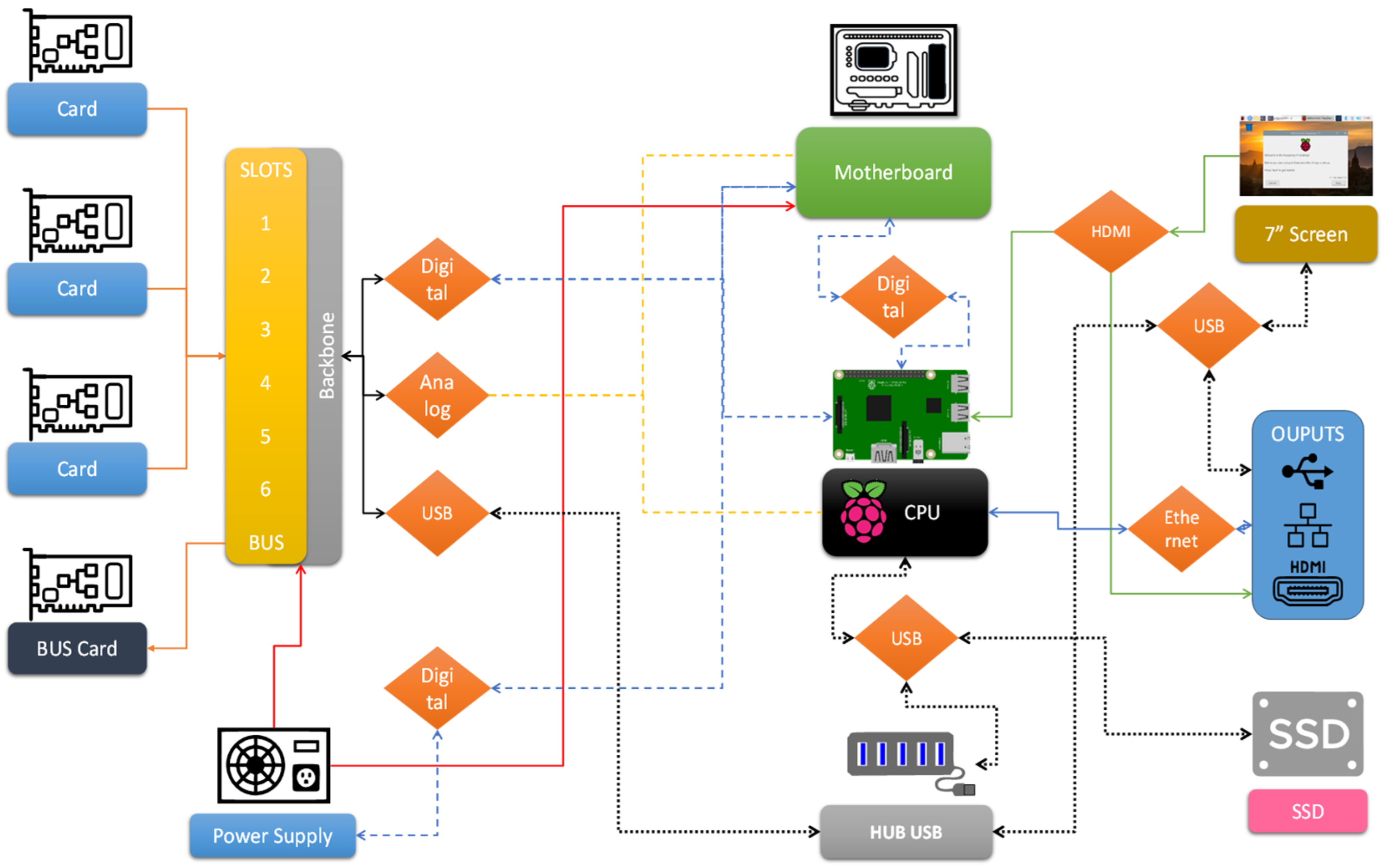
The name Nexus derives from the Latin word nectere, meaning “to bind” or “to connect” [34], reflecting the system’s intended role as a multichannel data acquisition platform designed to integrate multiple capture modules with interoperability across sensors, measurement platforms, and embedded systems. Designed as an open hardware platform [35,36,37,38], the system architecture is illustrated in Figure 1, which presents the internal organization and interconnections between the main functional blocks.
Figure 1 presents a connection-oriented architectural diagram of the Nexus system, illustrating the physical and logical interconnections between functional modules and communication interfaces. Solid orange lines denote external input connections, while solid red lines indicate power distribution paths. Dashed blue lines represent digital signal routing, and dashed yellow lines correspond to analog signal paths. Dotted black lines identify Universal Serial Bus (USB) communication links, and solid green lines indicate High-Definition Multimedia Interface (HDMI) connections. The acquisition cards, shown on the left, implement dual-channel inputs and interface with the backbone, which distributes power and routes analog and digital signals to the motherboard, CPU, and USB hub. The motherboard aggregates signal conditioning and power management, while the CPU is responsible for data processing, storage, and user interaction. Peripheral components, including the touchscreen interface, solid-state storage, and external communication ports, are integrated through standardized interfaces. The smart power supply maintains electrical connectivity with the system, enabling telemetry, controlled shutdown, and monitored power distribution.
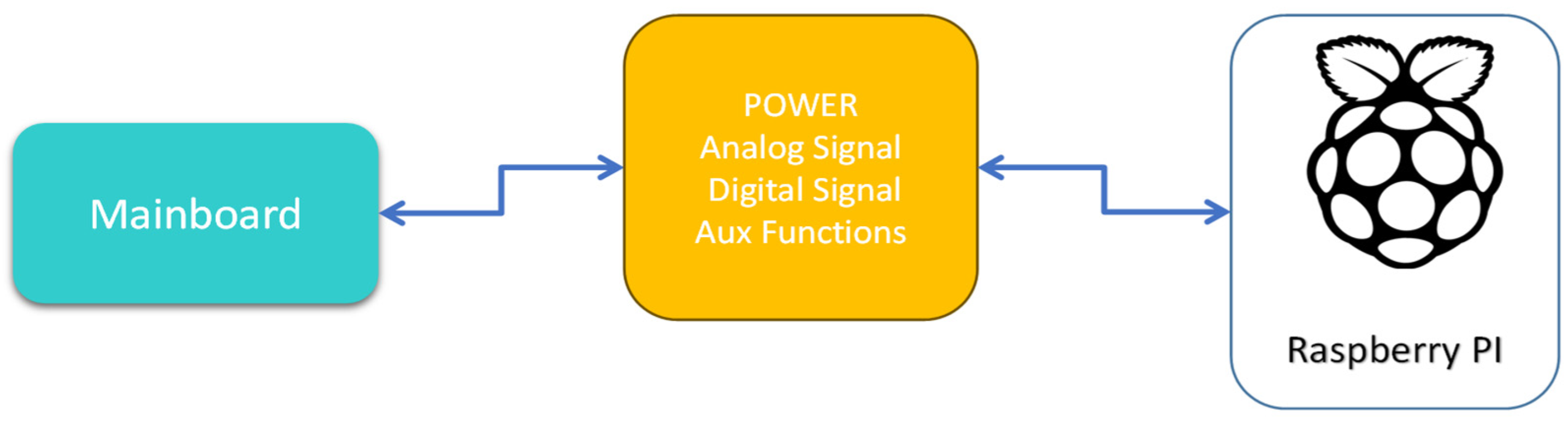
The Nexus data logger is composed of dedicated circuits responsible for data acquisition, processing, control, storage, and system interfacing. Its architecture is modular and consists of independent yet interconnected boards, with two main internal elements: (i) the backbone, which serves as the central bus connecting the acquisition cards to the remaining modules, distributing power and routing acquired signals either to the motherboard or directly to the CPU; and (ii) the motherboard, which is responsible for signal pre-conditioning, multiplexing, filtering, and communication between system layers, in addition to integrating logic control circuits and power monitoring. Figure 2 illustrates the overall data acquisition flow of the system. The input signal is first conditioned and digitized by the acquisition card. The backbone provides mechanical support and interconnection between modules. Finally, the mainboard routes the data to the Raspberry Pi for processing and storage.
Nexus employs interchangeable acquisition cards connected through a high-density backbone to the central motherboard. In this configuration, analog signals are digitized at the acquisition modules using either dedicated ADCs (ADS1256 (24-bit ADC), Texas Instruments, Dallas, TX, USA) or microcontroller-based converters and transmitted via dedicated communication buses (SPI, I2C, or UART, depending on the module) toward the central processing layer. The Raspberry Pi–based unit performs high-level control, data visualization, and storage management, writing the acquired data to local USB 3.0 SSD storage, with optional cloud synchronization. System coordination and deterministic data routing are ensured by the integrated motherboard–backbone interconnection, which mediates communication between acquisition modules, power management, and the user interface.
  • Acquisition cards ↔ Motherboard (SPI/I2C/UART + power rails).
  • Motherboard ↔ Raspberry Pi (USB/serial, storage control, UI).
  • Power subsystem ↔ Motherboard/RPi (telemetry, source switching, shutdown).
The data acquisition process follows five main stages: First, the sensor converts the physical quantity into an electrical signal, which is routed to the acquisition card, where preliminary amplification or filtering may be applied. Second, the card interfaces with the backbone bus, which transmits the signal to the central system circuits. Third, the signal is either forwarded directly to the CPU when prior conditioning is sufficient or routed through the motherboard, where it may undergo conditioning, digitization, or multiplexing. Fourth, data acquisition and visualization are performed by the Raspberry Pi 4B, which executes acquisition scripts, stores the data on the solid-state drive, and displays the signals on the touchscreen interface. Finally, the acquired data can be transmitted in real time via Ethernet or Wi-Fi, exported through USB interfaces, or stored locally for subsequent analysis. The acquisition cards of the Nexus system were designed to conform to the mechanical constraints of the enclosure, ensuring modularity, mechanical compatibility, and ease of maintenance. Their development integrated mechanical and electrical design considerations, with an emphasis on usability, standardization, and scalability. The physical layout was defined to support multiple input connector types (including BNC, 3.5 mm jacks, terminal blocks, and pin headers), provide sufficient space for amplifiers, filters, converters, and microcontrollers, promote logical component placement for efficient routing and passive ventilation, incorporate structural features for secure insertion into the chassis, ensure precise alignment of mounting holes, and maintain full enclosure of the cards within the device body. After several design iterations, the final card format was defined with external dimensions of 141 mm × 100 mm × 1.6 mm, excluding the PCI connector recess. Each card includes two M3 threaded holes for securing the front panel and user interface elements. A dimensional template was incorporated into a custom EagleCAD library to facilitate reuse and prevent layout incompatibilities in future designs, thereby supporting long-term scalability and collaborative development. The development of the Nexus platform involved a substantial iterative design effort, comprising approximately 1200 h of CAD modeling distributed over a five-month period. This process included the design of electronic and mechanical components, fabrication of test parts, multiple design revisions, and replacement of damaged prototypes. The final system comprises approximately 50 custom parts, excluding fastening elements, and required more than 500 h of additive manufacturing, consuming approximately 6 kg of PLA filament.
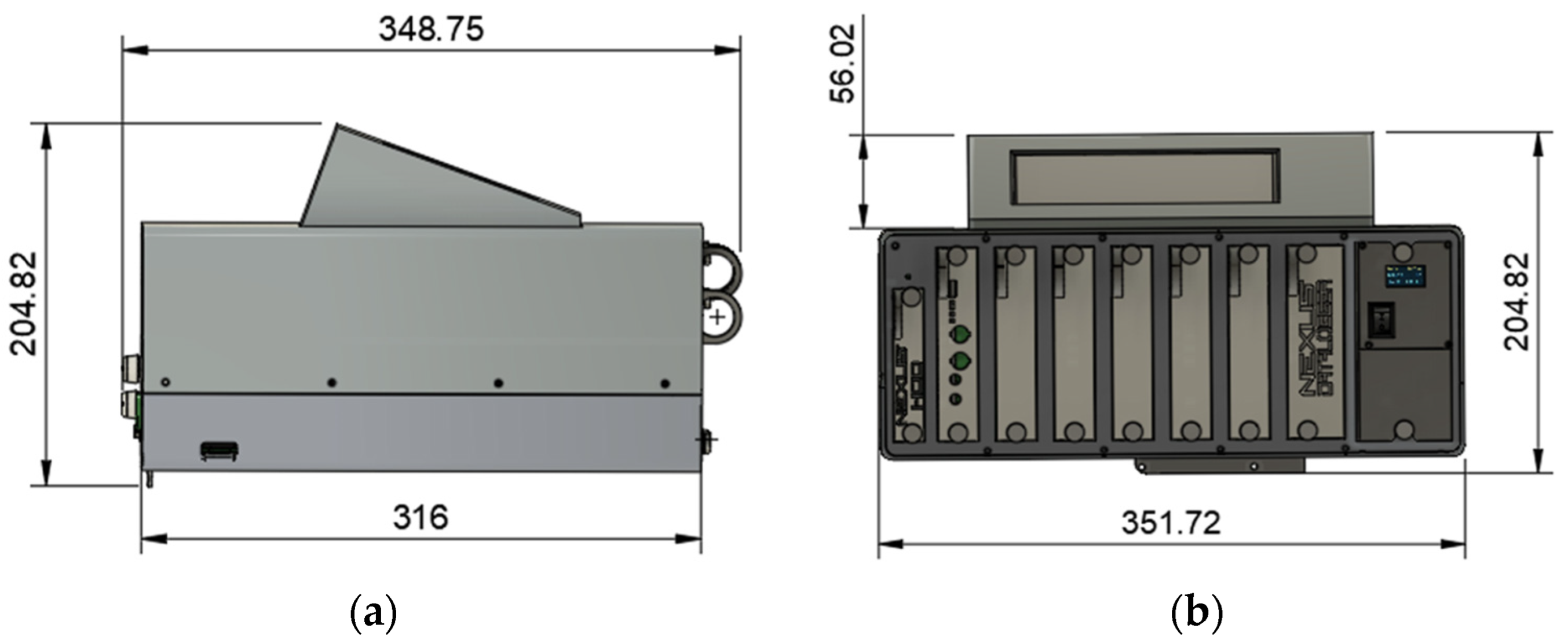
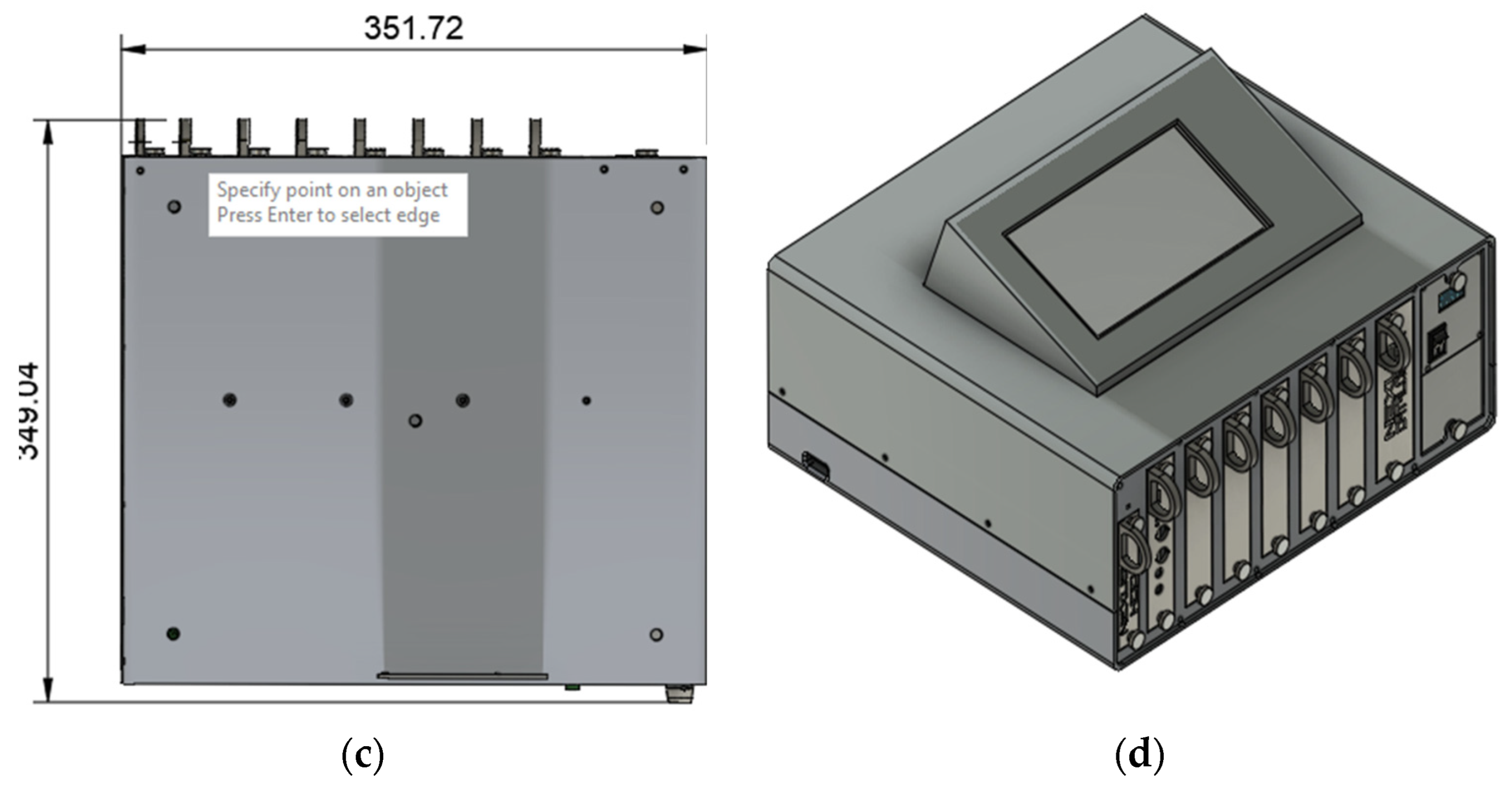
The final dimensions of the equipment are 351.72 mm × 349.04 mm × 204.82 mm (L × W × H), ensuring compatibility between internal components and the external structure, and enabling precise and functional assembly. Figure 3 shows the technical drawings with the main views: (a) side, (b) front, (c) bottom, and (d) isometric.

3. Development and Prototyping Process

This section presents the overall fabrication process of the Nexus proof of concept, encompassing the development and integration of its electronic, mechanical, and embedded components. The construction phase involved not only the design and assembly of printed circuit boards (PCBs) and module enclosures, but also the implementation of embedded firmware, graphical interface configuration, and system-level functional validation. Special attention was given to the use of components readily available in the domestic market, ensuring local reproducibility and cost-effectiveness. Mechanical considerations, including thermal management, modular layout, and ease of access, were addressed to support scalability and maintainability. An iterative prototyping approach was adopted, enabling the progressive refinement of signal integrity, power distribution, and shielding strategies across successive hardware revisions.

3.1. Hardware

The data logger is organized into two main control and processing elements: the motherboard and the central processing unit (CPU). In conventional architectures, the CPU is typically integrated into the motherboard; in the Nexus platform, however, these elements are intentionally separated to enhance modularity and facilitate processor replacement. The selected CPU is a Raspberry Pi 4 Model B (Raspberry Pi Foundation, Cambridge, UK), a Linux-based single-board computer that integrates processing, memory, wireless connectivity (Wi-Fi and Bluetooth), and peripheral support. This configuration enables rapid CPU replacement in the event of failure, system upgrades, or adaptation to new application requirements, without requiring modifications to the remaining hardware modules.
The motherboard, developed specifically for this project, operates as an auxiliary processing and control unit, organizing, formatting, and mediating the data received from the acquisition cards before forwarding them to the main processor. Beyond its auxiliary role, the motherboard functions as the central hub for power distribution, signal routing, and system-level communication, justifying its designation as the motherboard. Figure 4 presents a simplified communication diagram between the motherboard and the CPU, highlighting their direct and exclusive interconnection.
To improve the readability of the motherboard architecture, its functionality is described through five conceptual stages, each corresponding to a distinct functional role within the system. First, analog input signals are received and routed through dedicated front-end paths, while digital inputs are handled through independent logic interfaces, allowing both domains to be processed concurrently. Second, all input channels converge toward the central routing layer, where signal distribution and arbitration are managed to ensure deterministic communication between subsystems. Third, communication between the motherboard and the central processing unit is established through a dedicated interface, enabling direct and exclusive data exchange and coordination of acquisition tasks. Fourth, power management and system supervision are handled by a microprocessor-based power subsystem, which provides regulated supply lines, monitoring capabilities, and control signals to the remaining modules. Finally, the internal bus structure assigns dedicated, non-shared pins to each acquisition slot, configured either as general-purpose input/output (GPIO) lines or as auxiliary communication signals, such as Chip Select (CS), ensuring predictable routing, firmware traceability, and modular scalability. The detailed operation of each functional stage and its associated circuitry is described individually in the following diagram.
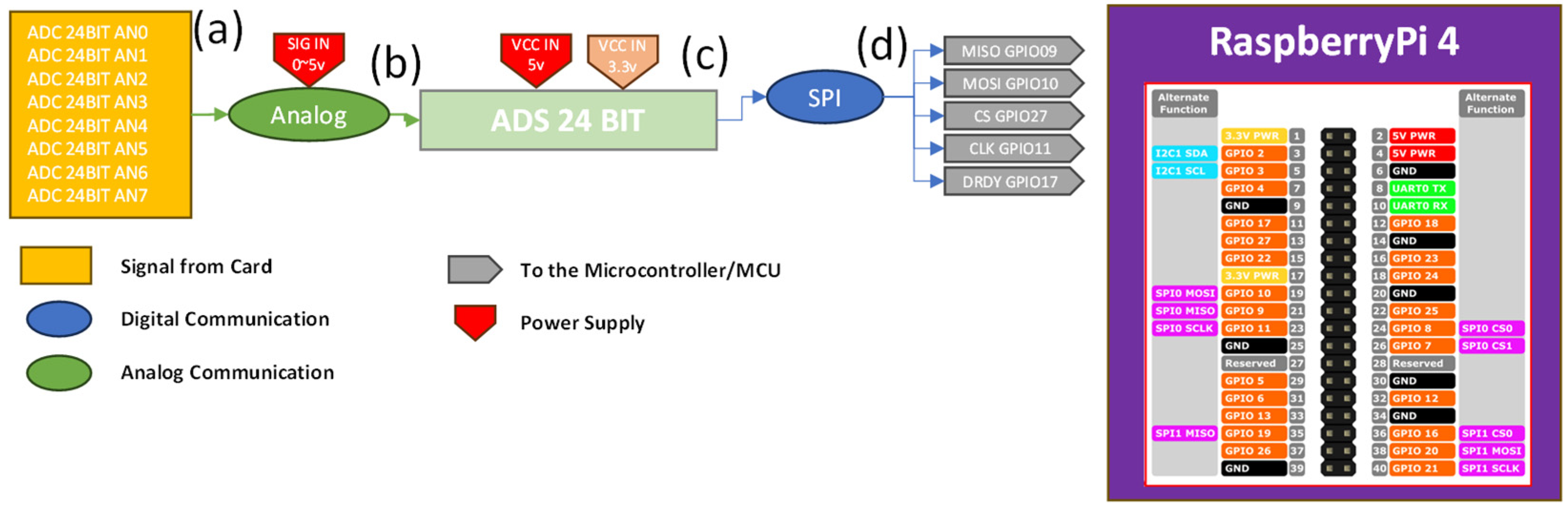
Diagram 1, illustrated in Figure 5, describes the 24-bit analog-to-digital conversion stage implemented on the motherboard using the ADS1256, with emphasis on data flow and functional interconnections. The diagram outlines the signal path from the analog input interface to digital communication with the central processing unit. As indicated in item (a), up to eight analog input channels, identified as AN0 to AN7, are available on the internal acquisition interface and can be sourced from any acquisition card inserted into slots 1 through 6. Item (b) represents the analog signal domain prior to digitization. Item (c) corresponds to the ADS1256 analog-to-digital converter, which performs high-resolution signal conversion. Item (d) illustrates the digital data exchange between the ADS1256 and the CPU, implemented via the Serial Peripheral Interface (SPI) protocol operating in master mode. An additional data-ready signal is used to indicate conversion availability. The SPI communication lines include MISO, MOSI, chip select (CS), clock (CLK), and a dedicated data-ready (DRDY) signal, enabling synchronized data transfer between the conversion stage and the processing unit.
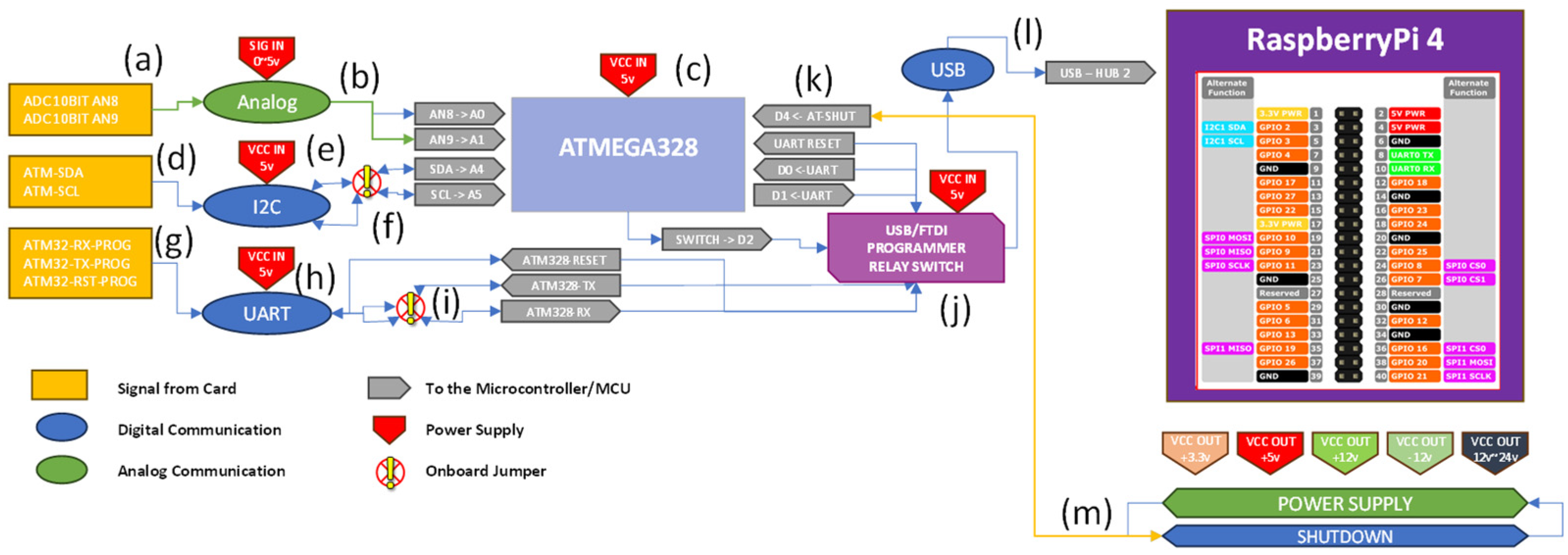
Figure 6, Diagram 2 illustrates the auxiliary interface circuit implemented using an ATmega328 (Microchip Technology Inc., Chandler, AZ, USA) microcontroller, referred to as auxiliary circuit 1, with emphasis on functional roles and data flow. This subsystem performs three primary functions: acquisition of two auxiliary analog inputs, communication via the I2C protocol in master mode, and operation as a configurable serial communication switch. As indicated in item (a), two auxiliary analog input channels, identified as AN8 and AN9, are routed to the ATMEGA328 for local acquisition. Item (b) represents the analog signal input pins prior to digital processing, while item (c) corresponds to the ATMEGA328 microcontroller responsible for coordinating acquisition, communication, and control tasks. Items (d) and (e) illustrate the dedicated I2C communication interface associated with the ATMEGA328, which enables data exchange with other system modules. A configurable selector, shown in item (f), allows reassignment of the I2C signal lines to support interface compatibility when required. The UART2 interface, shown in items (g,h), is dedicated to remote programming of the acquisition cards and is shared between the ATMEGA328 and the target card while item (i) indicates a configurable selector that enables reassignment of UART signal routing when necessary. Item (j) represents a relay-based switching stage controlled by the ATMEGA328, enabling dynamic selection of UART control between the microcontroller itself, the UART2 interface, or the connected acquisition card. (k) is the output to system shutdown that connects to (m). Item (l) illustrates the communication interface between the ATMEGA328 and the central processing unit, implemented through a USB-based connection on the motherboard. Finally item (m) represents an auxiliary control signal used to trigger a remote power management action when asserted for a predefined time interval.
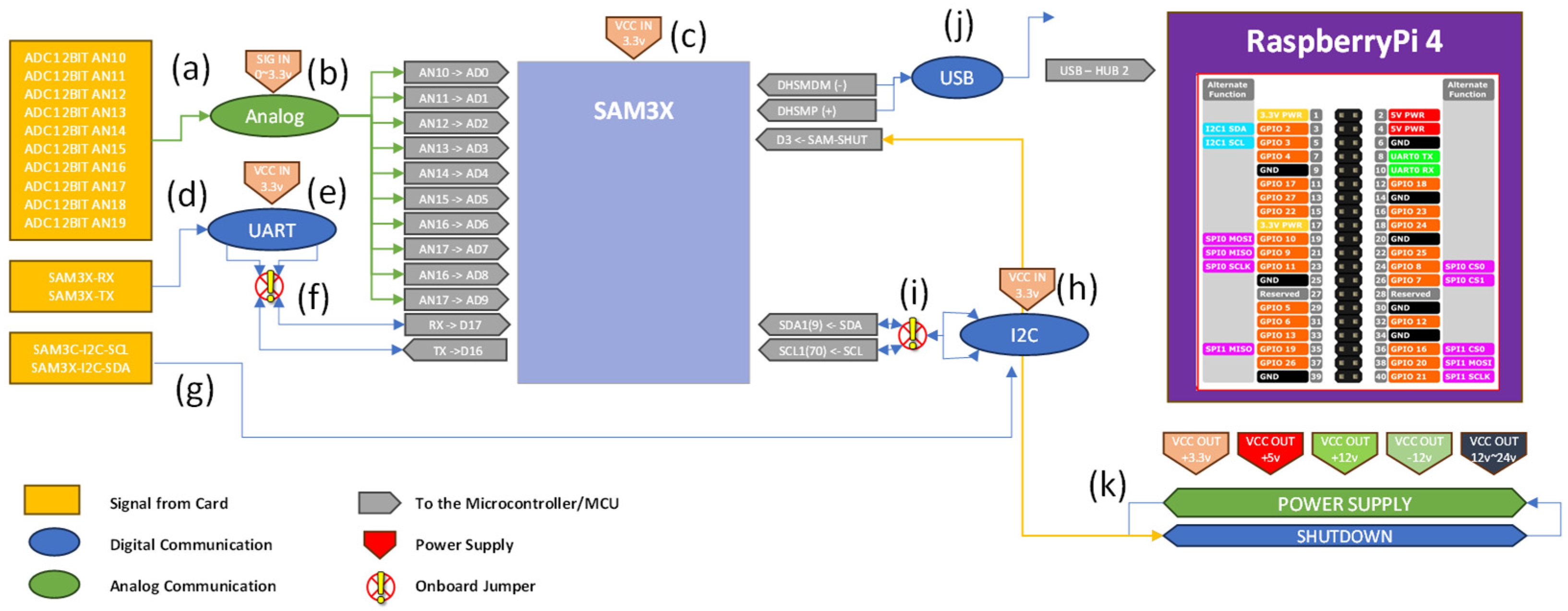
Figure 7 presents Diagram 3, which describes Auxiliary Circuit 2 implemented using an ATSAM3X microcontroller (Microchip Technology Inc., Chandler, AZ, USA), with emphasis on its functional roles and data flow. This subsystem performs three primary functions: acquisition of analog signals through an internal analog-to-digital conversion stage, serial communication via a UART interface, and digital communication using the I2C protocol operating in master mode. As indicated in item (a), multiple analog input channels, identified as AN10 to AN19, are routed to the ATSAM3X for signal acquisition. Item (b) represents the analog signal domain prior to digital processing, while item (c) corresponds to the ATSAM3X microcontroller, which coordinates acquisition, communication, and control tasks within this auxiliary circuit. Item (d) illustrates the UART-based serial communication interface associated with the ATSAM3X, enabling bidirectional data exchange with other system modules. A configurable selector, shown in item (e), allows reassignment of the receive and transmit signal routing to accommodate interface compatibility when required. Item (f) represents a physical jumper used to resolve potential UART signal mismatches. Item (g) denotes the I2C signal input to the ATSAM3X, while item (h) represents the set of I2C bus lines distributed to external peripherals. Item (i) illustrates a physical jumper used to correct potential I2C signal mismatches. Item (j) depicts the USB-based communication interface between the ATSAM3X and the remaining system infrastructure. Finally, item (k) represents an auxiliary control signal used to trigger a remote power management action when asserted for a predefined time interval.
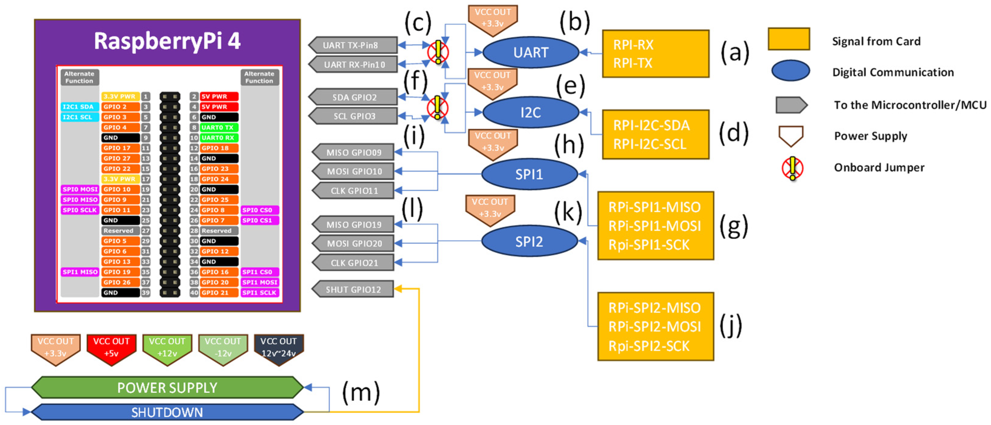
Diagram 4, illustrated in Figure 8, presents the direct digital interfaces between the central processing unit and the motherboard. This diagram highlights the connections that are routed directly to the CPU without intermediate switching or additional processing stages, emphasizing the functional data paths between system modules. As indicated in items (a) and (b), a dedicated UART interface provides serial communication between the motherboard and the CPU. A configurable selector, shown in item (c), allows reassignment of the receive and transmit signal inputs of the UART to the RPi. Items (d) and (e) represent the I2C input signal lines, with the signals routed to dedicated GPIO pins on the CPU. Item (f) denotes an onboard jumper used to correct potential signal mismatches. Items (g) and (h) illustrate the first Serial Peripheral Interface (SPI0), while item (i) details its corresponding input pins on the CPU, including MISO, MOSI, and clock signals. Items (j) and (k) present a second independent Serial Peripheral Interface (SPI1), with item (l) indicating its associated input pins on the CPU for MISO, MOSI, and clock. These two SPI interfaces enable high-speed digital communication with selected subsystems and support flexible data exchange and synchronization within the platform architecture. Finally, item (m) represents a dedicated control signal routed from the CPU to the power management subsystem; when asserted for a predefined time interval, this signal enables remote system shutdown.
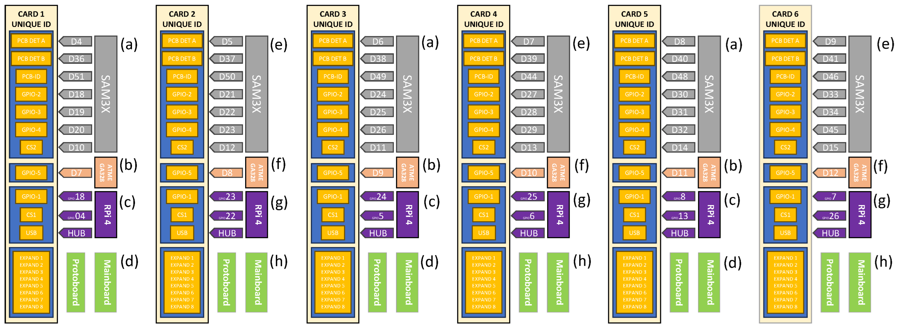
Figure 9 presents an overview of the individual I/O pin assignments associated with each acquisition card, highlighting the exclusive pins, their predefined functions, and their connection points within the Nexus system. Rather than representing a block diagram, this figure provides a consolidated mapping of the digital interfaces used for card identification, control, and communication. The connections are organized according to the responsible processing unit. For the ATSAM3X, the assigned pins include board type detection signals, a board identity line, three general-purpose input/output signals, and a dedicated chip-select line. The ATMEGA328 is assigned a single dedicated general-purpose input/output pin for auxiliary control functions. The central processing unit (Raspberry Pi 4B) provides a general-purpose input/output signal, a chip-select line, and access to the USB interface via the onboard hub. Additional expansion pins are reserved on the motherboard and remain available for future prototyping or system extensions.
The dedicated pins associated with each processing unit are identified as follows: items (a) and (e) correspond to the ATSAM3X, items (b) and (f) to the ATMEGA328, items (c) and (g) to the Raspberry Pi 4B, and items (d) and (h) to the mainboard prototyping area, which is not implemented at this stage. Figure 9 details the specific pin assignments for Cards 1 through 6, illustrating the consistent structure adopted across all slots while preserving independent addressing and control for each acquisition card.
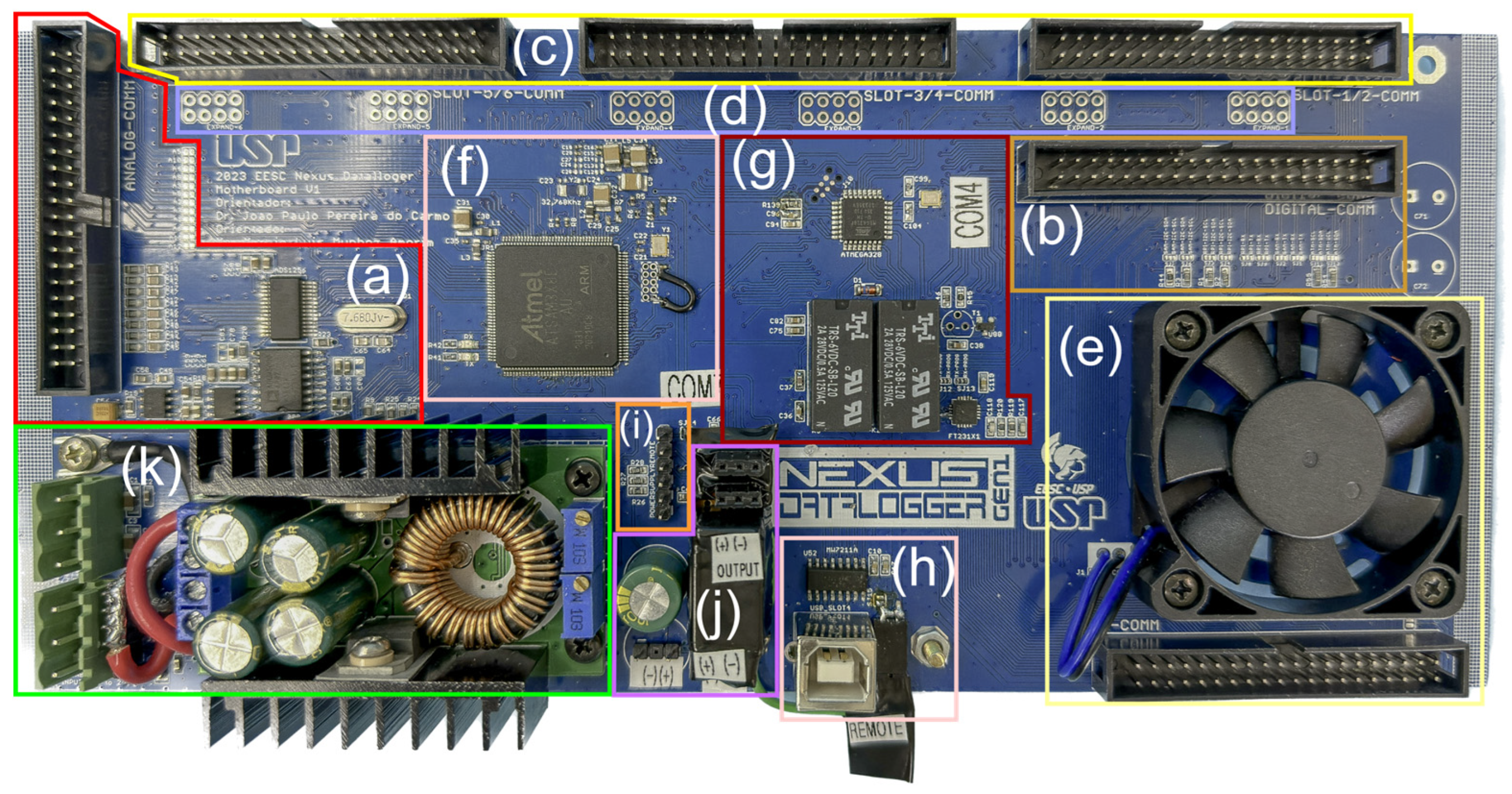
The motherboard is not implemented as a shield or prototyping board, where components are simply attached to a generic platform. Instead, it is a fully custom, large-scale PCB (108 mm × 245 mm) specifically designed to integrate all system subsystems in a single board, with dedicated and physically separated analog and digital ground planes. Figure 10 presents the motherboard segmented by functional blocks. In this figure, (a) corresponds to the analog input stage, which aggregates all analog signals routed to the ADS1256, ATSAM3X, and ATmega328 ADCs; this circuit operates with an isolated analog ground plane to minimize digital interference. Block (b) represents the digital communication inputs, including I2C, SPI, and UART interfaces. Block (c) shows the exclusive input pins for acquisition channels 1 to 6, distributed across three 40-pin headers. Block (d) corresponds to expansion headers, currently unused, which enable future hardware upgrades without requiring board replacement. Block (e) represents the output interface to the Raspberry Pi, as well as the dedicated fan used to assist thermal management of the CPU. Block (f) corresponds to the ATSAM3X microcontroller subsystem, while block (g) contains the ATmega328 auxiliary controller. Block (h) shows the onboard USB hub responsible for aggregating the acquisition card interfaces. Block (i) represents the UART communication interface with the smart power supply. Block (j) corresponds to the power-enable circuitry for both the USB hub and the Raspberry Pi. Finally, block (k) represents the main power input from the power supply subsystem, which also integrates an onboard 5 V/65 W regulator.
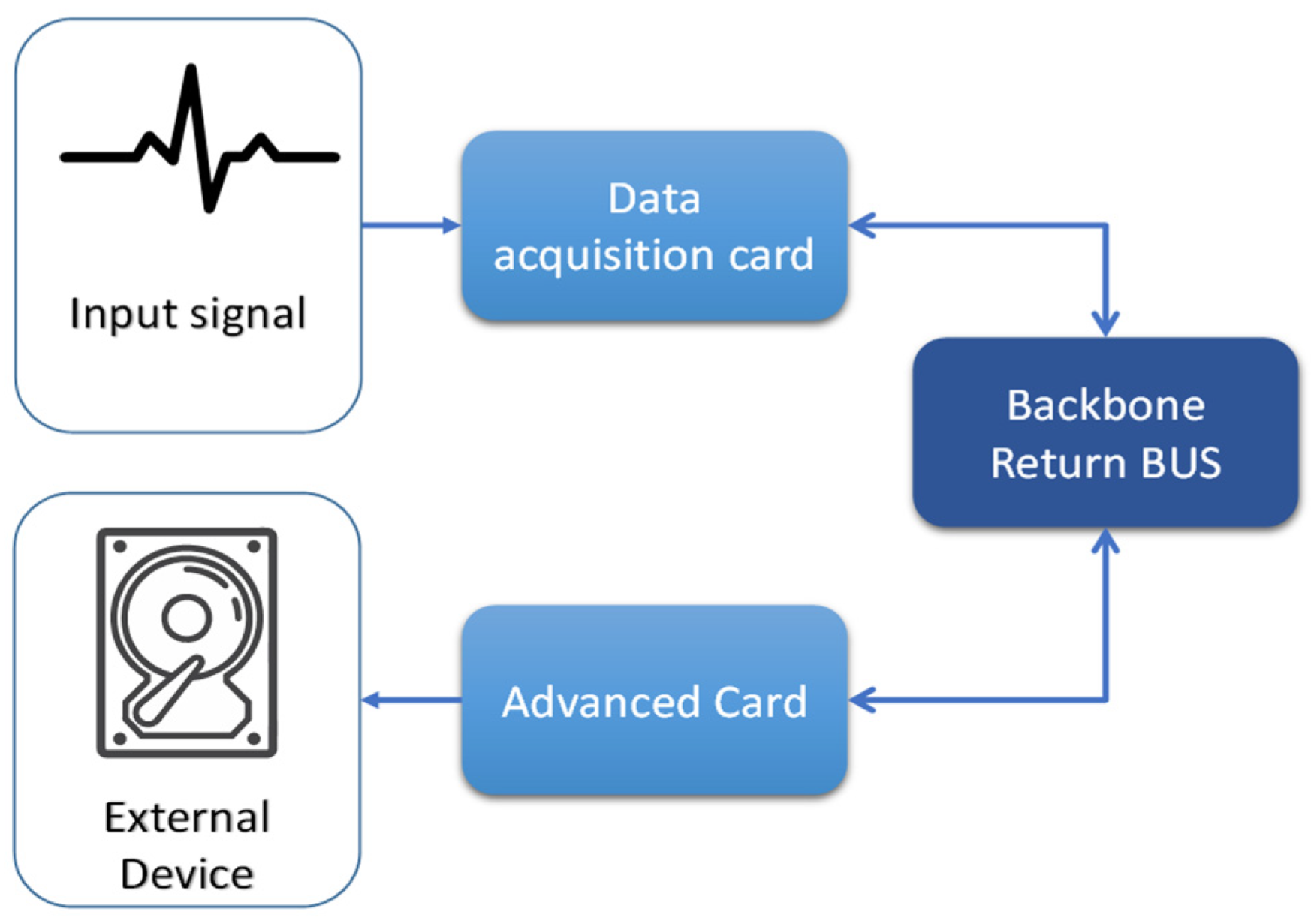
The data acquisition cards are inserted through the front of the data logger and connect directly to the main interconnection board, referred to as the Backbone. The term, derived from the anatomical concept of a spinal column, denotes the central structural and electrical interface through which signals and data are routed between system modules. The Backbone was designed to support six acquisition slots and a dedicated return channel, referred to as the return bus. This independent circuit enables the direct transmission of data from any acquisition card to a designated return card without passing through the system’s internal processing chain. Within the scope of this proof of concept, the return card operates as an expansion interface, allowing the integration of additional devices such as external storage units, higher-speed analog converters, or auxiliary communication interfaces. The return bus enhances the modularity of the platform by enabling future hardware extensions and alternative data routing strategies. Figure 11 presents a simplified representation of the return circuit. In this configuration, acquired signals may be routed directly to the return card without processing, enabling real-time recording or playback. A hybrid operating mode is also supported, in which signals are transmitted simultaneously to both the central processing unit and the return card. This approach enables use cases such as parallel local storage and remote transmission, including data transfer via optical fiber using high-speed converters, or via RS-485, a communication standard widely adopted in industrial environments.
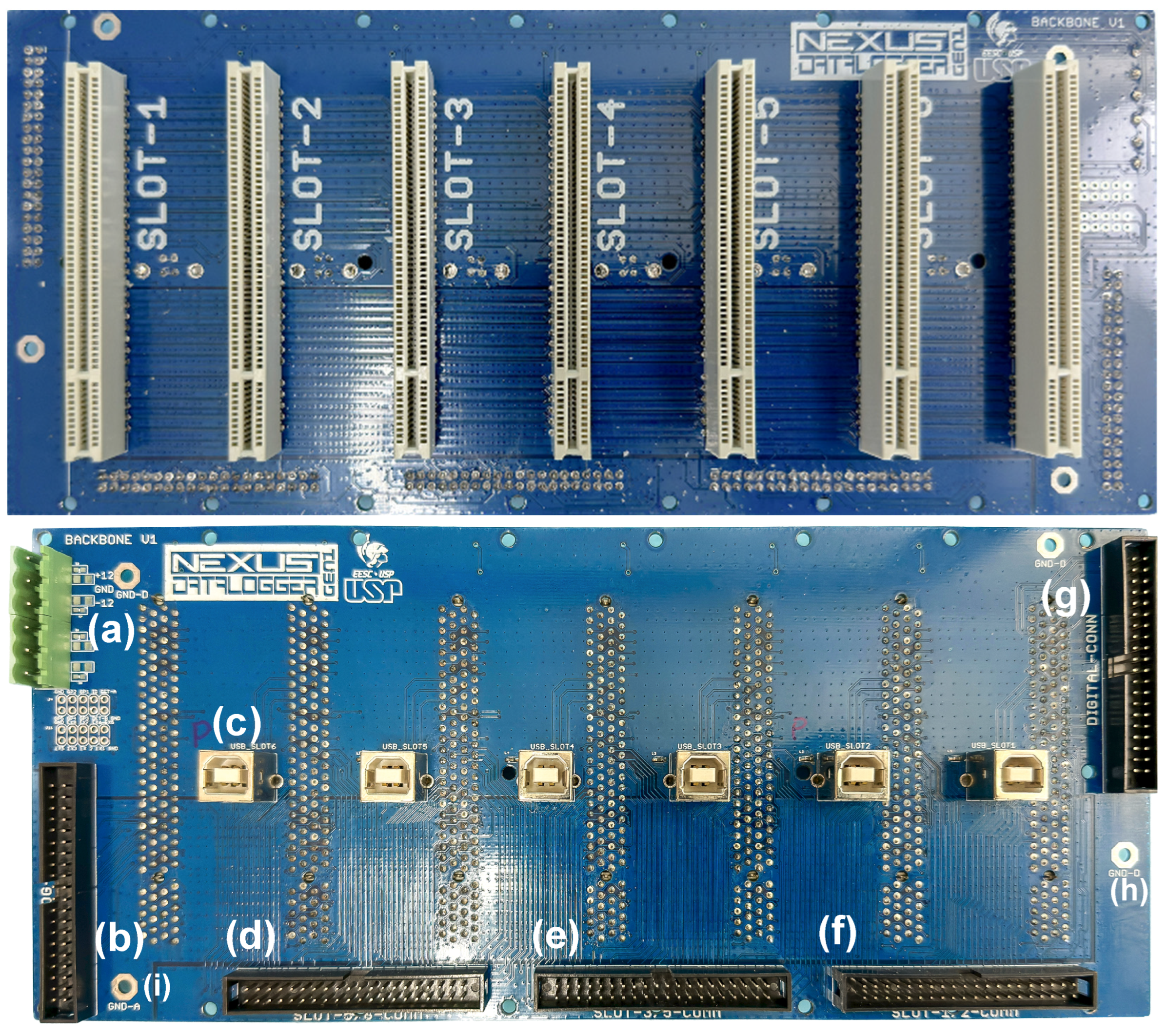
The Backbone board contains no active or passive components and is dedicated exclusively to structural support and electrical interconnection. Its primary role is to provide a centralized mechanical and electrical interface between the acquisition cards and the remaining modules of the data logger. All signal processing is therefore performed on the acquisition cards, on the motherboard, or on the central processing unit. Figure 12 presents the Backbone board from two complementary perspectives. The upper image shows the front side of the board, highlighting the physical arrangement of the card slots. Seven 120-pin PCI-type card-edge connectors manufactured by TE Connectivity (TE Connectivity Ltd., Schaffhausen, Switzerland) are positioned sequentially along the board: Slots 1 to 6, arranged from left to right, are dedicated to acquisition cards and operate independently according to their respective configurations, while Slot 7, located at the far right, is reserved exclusively for the return card, providing a direct data output path for signals routed from any acquisition card. The lower image shows the rear side of the Backbone board, where power distribution and external interface connections are located. The labeled elements include: (a) power input connectors distributing the required supply rails; (b) a 40-pin connector providing direct access to analog signals from the acquisition cards; (c) six USB Type-B connectors, one per acquisition slot, enabling communication with card microcontrollers; (d–f) dedicated multi-pin connectors grouping control and digital signals for pairs of acquisition cards; (g) a general-purpose digital connector aggregating shared interfaces such as SPI, I2C, and UART; and (h,i) separate digital and analog ground connections, supporting signal integrity through physical grounding separation.

3.2. Schematic

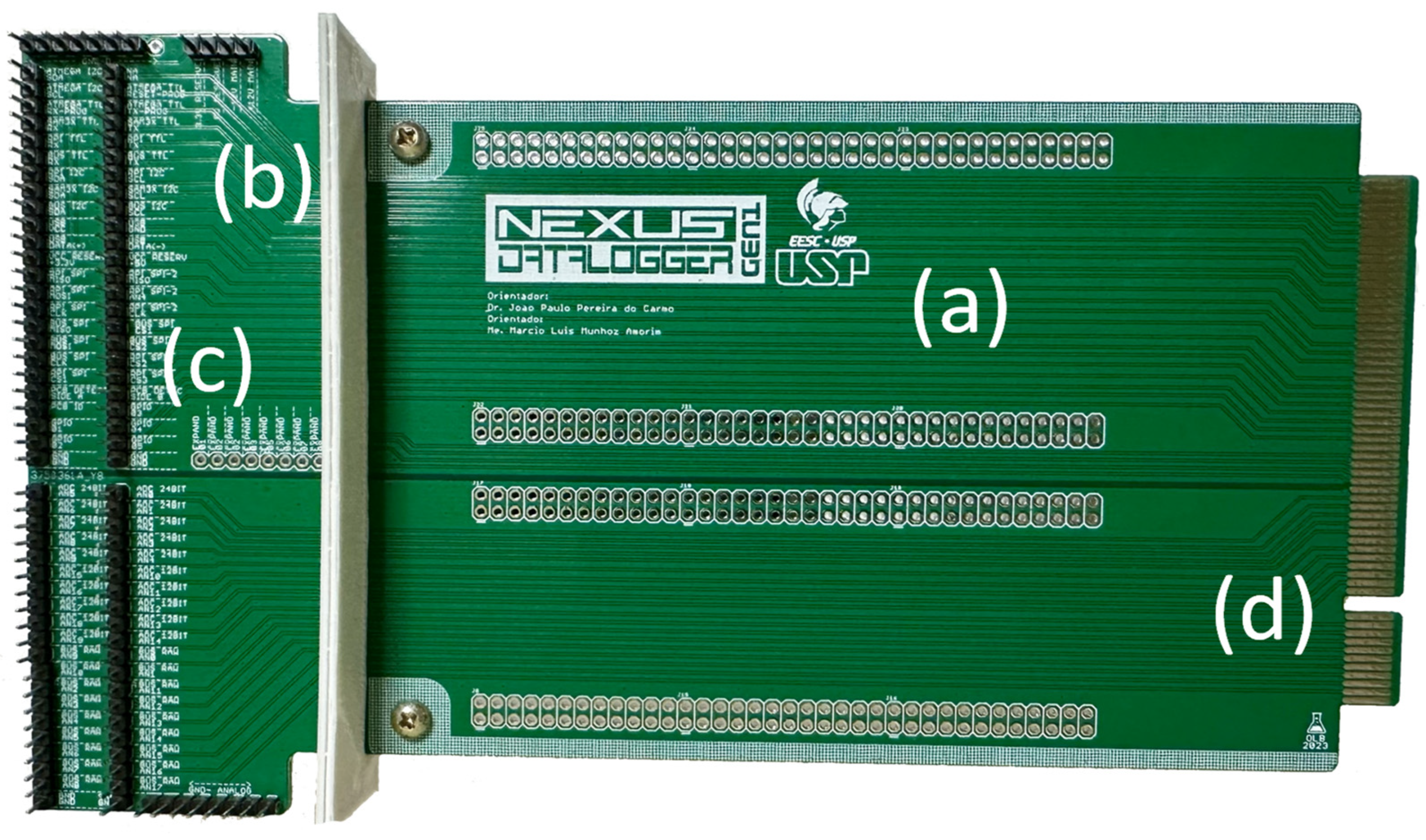
The Backbone board incorporates a simplified electronic circuit dedicated exclusively to the structural and electrical interconnection of the system modules. Its design is centered on providing a uniform and reliable interface between the acquisition cards, the return bus, and the remaining subsystems of the data logger. The board integrates seven identical PCI connectors. Six of these connectors are allocated to the acquisition cards, enabling direct signal exchange with the system infrastructure, while the seventh connector is reserved for the return bus. For the acquisition slots, the PCI connectors are electrically linked to auxiliary multi-pin interfaces that extract control and digital signals such as general-purpose input/output lines, chip-select signals, and auxiliary control lines, as well as to dedicated USB ports that allow direct communication with the onboard microcontrollers or external computers. Although physically identical to the acquisition slots, the connector associated with the return bus serves a distinct function. It enables direct signal routing from any acquisition card to external modules without passing through the internal processing stages of the system. Within the scope of this proof of concept, the return bus operates as an expansion interface, supporting real-time signal output and the integration of additional hardware modules. Centralized power distribution is implemented at the base of the Backbone board, supplying the acquisition slots, the return bus, and the associated USB interfaces. Provision was made for local decoupling capacitors through dedicated pads on the printed circuit board; however, these components were not populated in the current revision, as they were not required during initial functional testing. The reserved pads remain available for future hardware revisions should additional local noise filtering become necessary. Based on the previously described signal distribution model and the standardized physical format of the acquisition cards, a dedicated board was developed to support functional testing and small-scale validation of the data logger. This board was conceived to evaluate the PCI-120 connector functionality and to verify connection integrity and communication efficiency between system modules during development and maintenance. The GPIO_tester card was implemented in the standard PCI-120 form factor to enable practical validation of all bus connections. Its main distinguishing feature is the physical extension beyond the enclosure, which allows direct access to signals while the card remains inserted, enabling real-time testing with external instruments without system disassembly. The card contains no active or passive electronic components and functions solely as an interconnection bridge between the PCI-120 connector on the Backbone board and a set of externally accessible 2.54 mm connectors, ensuring simplicity and reliability. All signal traces from the PCI-120 connector are routed directly to the external connectors in an organized layout designed to minimize connection errors. The separation between analog and digital ground domains is strictly maintained, preserving the system’s galvanic isolation. Two independent ground buses are externally accessible, providing direct reference points that improve measurement safety and accuracy. The GPIO_tester card was successfully assembled, including the installation of the 2.54 mm connectors and a custom 3D-printed front panel for system integration. Figure 13 shows the completed card with its main elements identified. The protective cover provides mechanical robustness, while the internal and external regions enable straightforward interfacing with the Backbone board and access to analog and digital test points. This structured layout supports reliable signal validation and educational use.
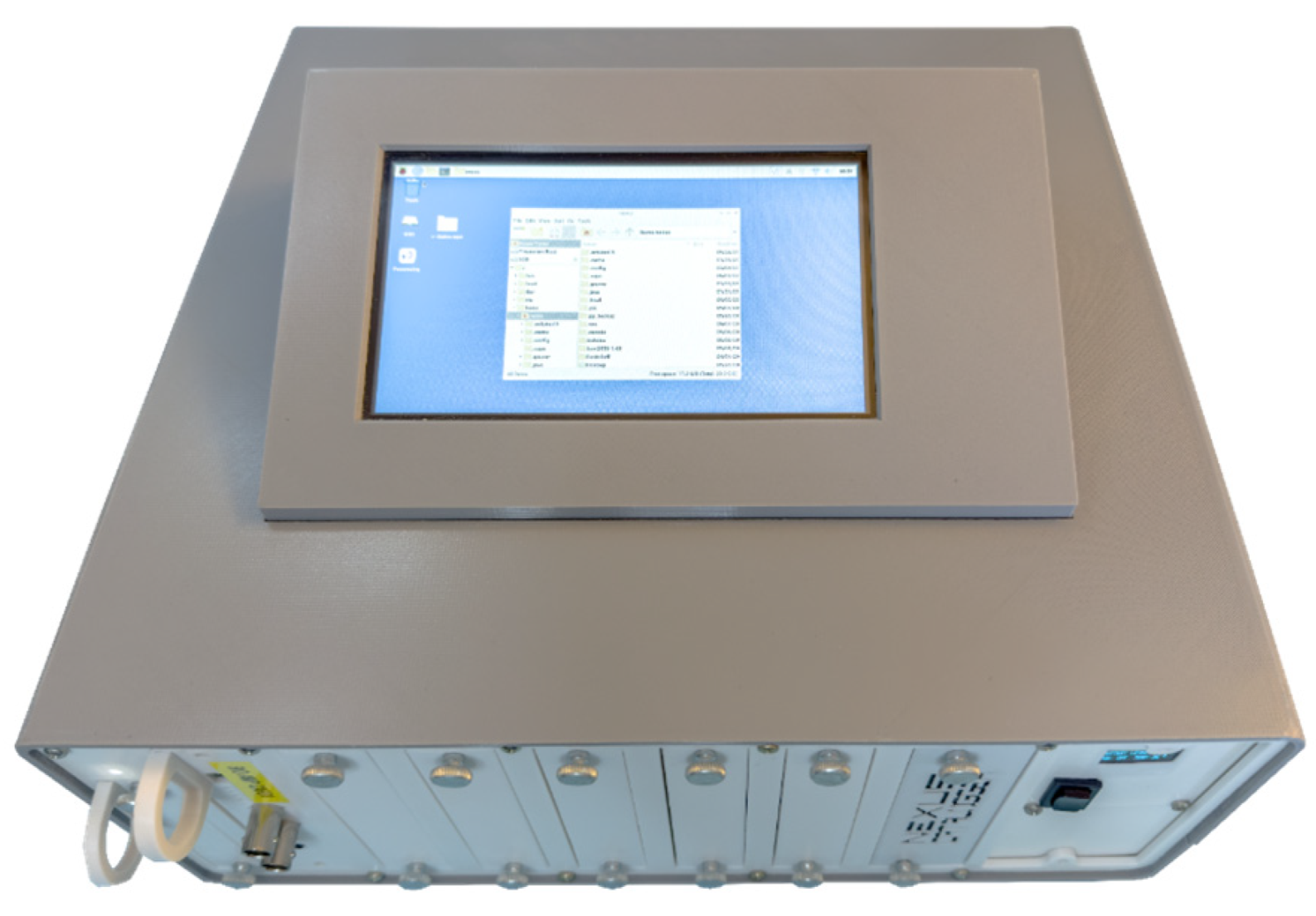
Figure 14 shows a photograph of the data-logger in operation, with the screen displaying the system’s file manager, demonstrating the proper functioning of the graphical interface.

3.3. Running Software and Software Interfaces

The system integrates six USB interfaces, one dedicated to each acquisition card, enabling direct communication between the card-level microcontrollers and the central processing unit. Each acquisition card incorporates either an embedded microcontroller with native USB support or a dedicated USB interface, allowing it to be recognized as an independent device by the operating system. All USB connections are aggregated through an internal USB hub Figure 15, which provides a single upstream interface to the CPU. This architecture simplifies device management, supports hot-plug detection, and enables parallel communication with multiple acquisition cards. Under the Linux operating system running on the Raspberry Pi, connected cards are automatically enumerated as USB devices, allowing straightforward verification of connectivity and interface status using standard system utilities.
I2C communication can be established either between the card and the motherboard or between the card and the CPU. This connection is made directly between the devices, involving their respective microcontrollers (MCUs) or the CPU itself. Figure 16 presents the I2C communication diagram, illustrating the interconnection structure between the system components and highlighting the simplicity and efficiency of this protocol for data exchange over a shared bus.
On the motherboard, I2C communication is supported by two dedicated microcontrollers, the ATMEGA328 and the ATSAM3X, each operating on an independent I2C channel. In addition, the central processing unit and the return bus also provide access points to the I2C infrastructure, enabling flexible communication paths between system modules. Although multiple connection points are available, the system architecture is organized into two independent I2C buses, allowing device addressing and communication to be managed without contention. Under the Linux operating system running on the CPU, connected I2C devices can be identified using standard bus-scanning utilities, such as the i2cdetect command, which enumerates active device addresses on the selected bus and supports interface verification during development and testing. Serial Peripheral Interface (SPI) communication can be established between acquisition cards and the CPU to support high-throughput digital data exchange. In addition to these shared interfaces, the system implements a dedicated SPI channel reserved exclusively for the 24-bit analog-to-digital converter. This converter operates on a separate SPI bus, isolating high-resolution analog acquisition from other digital traffic. Figure 17 presents the SPI communication architecture, illustrating the interconnection structure between system modules and highlighting the use of a dedicated SPI channel for the analog conversion stage.
The Serial Peripheral Interface (SPI) is enabled on the Raspberry Pi through the system configuration and is used to support digital communication with peripheral devices, including analog-to-digital converters. In the Nexus platform, SPI communication is employed for high-resolution signal acquisition using the ADS1256 converter, which supports up to eight analog input channels. The SPI is exposed in the operating system as standard device nodes, allowing access through user-level applications. Software interaction with the SPI interface is implemented using Python 3.10 in the Raspberry Pi OS environment. Standard libraries are employed to initialize the SPI bus, configure communication parameters, and manage chip-select signaling, enabling flexible control of the acquisition process during development and testing. Serial communication via the Universal Asynchronous Receiver–Transmitter (UART) interface can be established between the ATMEGA328, the ATSAM3X, and the central processing unit. This interface supports direct data exchange among system components and is commonly used for debugging, monitoring, and inter-module communication. Figure 18 presents the UART communication architecture, illustrating the simultaneous connectivity between the acquisition cards and both microcontrollers as well as the CPU. Under the Linux operating system, available serial interfaces are enumerated as device nodes, allowing straightforward identification and access during system operation.
Several software routines were developed to support functional testing and validation of the Nexus proof of concept. These routines were implemented in both C+ via Arduino IDE, Visual Studio and Python 3.10 Via PyCharm 2024.2.6 and Tonny 3.0.1, according to the requirements of each communication interface and subsystem. The complete source code is publicly available in a GitHub 2.52.0 repository to ensure transparency and reproducibility. The implemented routines cover key system functionalities, including detection and scanning of I2C devices, evaluation of I2C communication latency, acquisition of environmental data from I2C sensors, verification of SPI communication with high-resolution analog-to-digital converters, validation of UART-based data exchange, and performance testing of USB interfaces. Additional routines support dynamic switching between communication channels, evaluation of power supply behavior, and end-to-end system operation. A central Python script coordinates system initialization, interface management, and data acquisition, serving as the main software entry point for operating the platform during testing and validation.

4. Validation and Experimental Results

This section presents the experimental validation of the Nexus proof of concept under representative signal acquisition conditions. A series of functional tests was conducted to verify the correct operation and integration of the platform across its analog and digital acquisition subsystems. The evaluation focused on the acquisition of representative synthetic and biological signals using the integrated 24-bit, 12-bit, and 10-bit analog-to-digital converters, as well as on the verification of communication integrity over the I2C, SPI, and UART interfaces. In addition, the internal solid-state data logging, cloud backup routines, and touchscreen-based human–machine interface were exercised under extended operating sessions to confirm stable system behavior and coordinated interaction among subsystems. The results demonstrate the feasibility of the proposed architecture, functional completeness of the acquisition chain, and consistent operation during simultaneous multi-interface acquisition scenarios.

4.1. Power Quality Testing on the Cards

The voltage levels supplied to the acquisition cards were verified to confirm correct operation of the power distribution infrastructure. Measurements performed using the GPIO_tester card indicated that the ±12 V, +5 V, and +3.3 V rails remained within ±5% of their nominal values across all six slots. These results are consistent with the expected operating range of the system and confirm proper power delivery to the acquisition modules during representative operating conditions.
A communication test was performed to verify UART data exchange between the power supply module and the data logger, enabling real-time access to telemetry parameters. A dedicated software routine was developed to establish serial communication with the CPU, receive the data transmitted by the power supply, and present the information during system operation. The results confirmed reliable UART communication, with telemetry data being consistently received and correctly interpreted by the system. This functionality supports continuous supervision of power-related parameters and contributes to monitoring system operation during representative use conditions.

4.2. Inter-Integrated Circuit (I2C) Communication Test

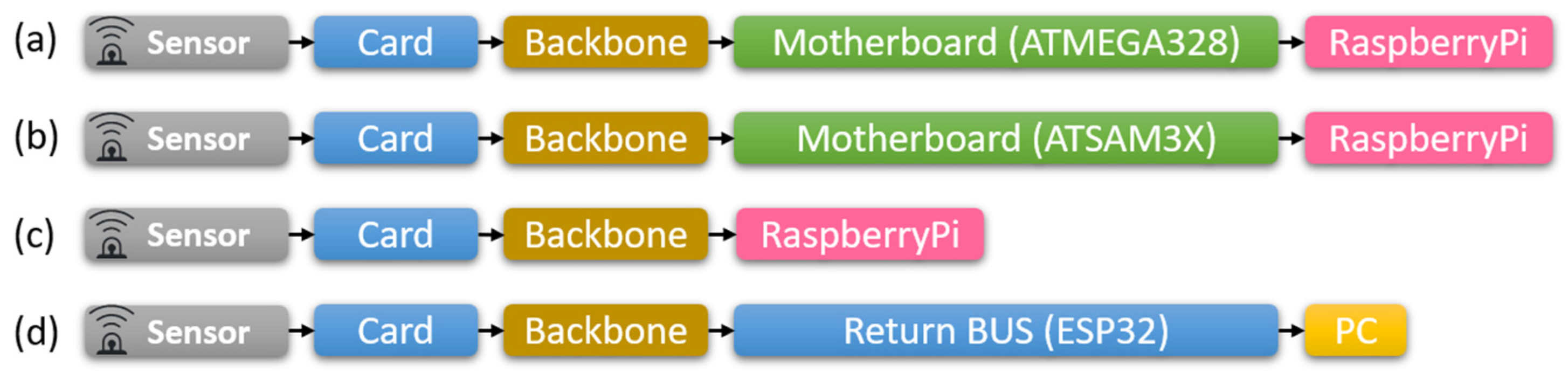
The objective of the I2C communication test was to validate the protocol’s operation in inter-device communication among the cards, MCUs, and CPU. The results confirmed the robustness and flexibility of the Nexus architecture across different I2C topologies. Figure 19 illustrates the four test configurations: (a) sensor data transmitted via Backbone → MCU II → CPU; (b) data sent via Backbone → MCU I → CPU; (c) direct sensor-to-CPU communication without intermediaries; and (d) data routed through the Backbone to the return card, where the ESP32-Thing+ Espressif Systems Co., Ltd., Shanghai, China processes the data and forwards it via USB to an external computer.
The I2C communication tests were performed using the GPIO_Tester card, which was developed to verify bus connectivity and signal integrity across the modular architecture. Two I2C sensors were connected in parallel to the system: an MLX90614ES-Melexis NV, Ypres, Belgium, infrared temperature sensor and an SI7021-Silicon Laboratories Inc., Austin, TX, USA humidity sensor. Both devices were interfaced through the shared I2C lines and powered using the 3.3 V supply and digital ground provided by the system. Communication was evaluated across multiple control points, including the ATMEGA328, the ATSAM3X, the central processing unit, and the return card, demonstrating the ability of the platform to support different I2C communication paths. The tests were repeated for all six acquisition slots, ensuring full coverage of the modular structure and consistent behavior across card positions. The results confirmed correct I2C communication and device detection in all evaluated configurations, supporting the feasibility of the proposed architecture for flexible sensor integration and inter-device communication over a shared bus.
All software routines used in the I2C validation tests are publicly available in the project’s GitHub repository, ensuring reproducibility. Four dedicated programs were developed to evaluate I2C communication under representative operating conditions. The validation process comprised device detection, communication timing analysis, sensor data acquisition, and stress scenarios involving bus sharing and dynamic reconnection.
Device detection was first verified using an I2C scanning routine, which consistently identified all connected devices and their respective addresses across all acquisition slots. Communication performance was then evaluated using a dedicated timing routine, while functional data transmission was validated through continuous acquisition of temperature and humidity data from infrared and environmental sensors. Each test was executed for 30 min per sensor and per microcontroller, either individually or concurrently, providing sufficient observation time to assess stability and repeatability. In addition to standard communication tests, two stress conditions were evaluated. In the chain test, multiple I2C devices were connected simultaneously to the same bus, verifying correct address-based communication without conflicts. In the hot-swap test, devices were physically disconnected and reconnected while the system remained powered and operational, demonstrating reliable device re-detection and communication recovery without requiring a system reset. Communication timing was quantified by estimating the effective transaction rate of the I2C bus. The I2C timing routine measures the round-trip latency Δt between the initiation of a write request and the completion of the corresponding read operation. Considering N pulses as the total number of SCL clock pulses involved in the transaction, the effective transaction rate is defined as
f S C L = N p u l s e s t
where Δ t = t r e s p o n s e t r e q u e s t . In practice, Δ t includes both transmission time and device response latency. For reporting convenience, results are expressed in kilohertz:
f S C L , k H z = N p u l s e s   ×   1000 t μ s
This metric does not represent the physical SCL clock frequency, which is typically fixed (≈100 kHz), but rather an effective transaction rate that captures end-to-end communication latency, including protocol overhead and sensor internal conversion times. Table 1 summarizes the results obtained with sensors connected to MCU II (ATMEGA328) across all six slots. The data include sensor type, I2C address, effective transaction rate, measured values, support for parallel device operation (chain mode), hot-swap behavior, and the occurrence of transmission errors. The results show consistent communication behavior across all slots, with successful operation in both chain and hot-swap configurations and no observed transmission errors. These findings demonstrate stable and reliable I2C communication under practical operating conditions, supporting the feasibility of the proposed modular architecture. In the following tables, ETR (End-to-End Transfer Rate) denotes the effective application-level data transfer rate. The columns indicate: slot (tested slot number), MCU (microcontroller in use), sensor (active sensor), addr. (device address), data (valid sensor data), I2C Chain (presence of multiple devices in the daisy chain), Swap (hot-swap capability), and error (observed transmission errors).
Table 2 summarizes the I2C communication tests performed with sensors connected to MCU I (ATSAM3X), organized by acquisition slot. The table reports the slot number, associated microcontroller, sensor type, I2C address, effective transaction rate (ETR, in kHz), received sensor values, support for parallel device operation (Chain), hot-swap behavior (HotSwap), and the occurrence of transmission errors. The results provide a comparative view of I2C communication behavior when mediated by the ATSAM3X microcontroller across different card positions. Consistent communication was observed in all evaluated slots, with successful operation under both parallel device connection and hot-swap conditions. These results support the feasibility of using MCU I as an I2C controller within the proposed modular architecture and demonstrate stable behavior under representative dynamic operating scenarios.
The test performed on the return bus (slot 7) was intended to verify its ability to operate independently of the data logger’s internal processing resources. In this configuration, the Nexus platform functions exclusively as a communication and power interface, without engaging its onboard computational units. The return bus is designed to route digital and analog signals from the acquisition cards directly to external devices, enabling integration with other platforms and supporting expanded testing scenarios. For this evaluation, the GPIO_tester card was configured as a return card and inserted into slot 7. Sensor data were routed through the return bus to an external ESP32 Thing+, which was connected via jumper wires to the GPIO_tester and interfaced through USB with an external computer executing the same I2C routines used in the previous validation tests. This setup allowed the assessment of data transmission through the return bus without mediation by the central processing unit. Table 3 summarizes the results obtained with sensors transmitting data via the return bus to the ESP32 Thing+. The data are organized by acquisition slot and include the microcontroller type, sensor model, I2C address, effective transaction rate (ETR), received values, support for operation without parallel devices (Chain), hot-swap behavior (HotSwap), and the occurrence of transmission errors. The results confirm that the return slot supports reliable I2C data transmission to external devices without involvement of the data logger’s CPU. These findings demonstrate the feasibility of using the return bus as an auxiliary interface for external integration and system-level testing.
The I2C communication tests involving the central processing unit (Raspberry Pi) exhibited behavioral differences when compared to those performed with the microcontroller-based subsystems. Owing to its Linux-based operating system, the CPU demonstrated distinct characteristics in I2C communication. Device detection was successfully achieved, with both the SI7021 and MLX90614ES sensors being correctly identified on the bus. However, despite repeated attempts and sensor replacement, reliable data acquisition from the SI7021 could not be established, and no evident electrical conflicts or addressing errors were observed. During the hot-swap evaluation, reconnecting an I2C sensor while the system remained powered led to a temporary lockup of the CPU’s I2C interface, requiring a system reboot to restore communication. These observations indicate that, although the CPU supports I2C device detection and basic communication, it is more susceptible to failures under dynamic operating conditions than the microcontroller-based interfaces. This behavior highlights the importance of accounting for differences between general-purpose operating systems and embedded controllers when designing robust and fault-tolerant data acquisition architectures. Table 4 summarizes the results obtained with the MLX90614ES sensor, organized by acquisition slot. The table includes the microcontroller or processing unit used, sensor type, I2C address, effective transaction rate (ETR), received data, operation under parallel bus conditions (Chain), hot-swap behavior, and the occurrence of transmission errors.
The tests showed consistent I2C communication between all acquisition cards and their respective controllers under the evaluated conditions. Variations in the observed communication timing were associated with differences in the characteristics of the employed microcontrollers. Hot-swap operation was successfully demonstrated when using the ATMEGA328, ATSAM3X, and ESP32 microcontrollers. In contrast, the Raspberry Pi exhibited limitations during dynamic I2C operation, including loss of communication during hot-swap events and restricted compatibility with one of the evaluated sensors. These observations indicate that, within the scope of the proposed architecture, microcontroller-based interfaces are better suited for handling dynamic I2C interactions, while CPU-based interfaces are more appropriate for controlled or application-specific use cases.

4.3. Serial Peripheral Interface (SPI) Communication Test

The SPI protocol was also tested to verify its operation between the cards and the data-logger. In the evaluated system, SPI is present exclusively on the CPU and is accessed through the return bus. The CPU has two SPI communication ports, referred to as SPI0 and SPI1. The SPI signal path can be seen as shown in Figure 20.
For the SPI communication test, a microSD card reader was employed to evaluate data transfer over the SPI bus under representative operating conditions. The test setup consisted of a microSD adapter connected to an 8 GB Class 10 memory card, formatted with the FAT32 file system and a block size of 4096 bits. The adapter interfaces with the system using six digital connections: power (3.3 V), ground, and the four SPI signals (MISO, MOSI, SCLK, and CS). The microSD reader was connected through the GPIO_tester card and evaluated across all acquisition slots (1–6). For tests involving the central processing unit, the secondary SPI (SPI1) was used. Data transfer was assessed using a dedicated test routine, in which a 32-bit data word (4 bytes) was written to the memory card and subsequently read back. The elapsed time Δt between the start of the write operation and the completion of the read operation was measured to estimate the effective transaction rate (ETR). The ETR was calculated based on the payload size and the measured latency, expressed both in megabits per second (Mbit/s, decimal) and mebibits per second (Mib/s, binary), as defined in Equations (3) and (4).
E T R M b i t / s = 8   ×   T o t a l B y t e s t s   ×   10 6
E T R M b i t / s = 8   ×   T o t a l B y t e s t s   ×   2 20
with TotalBytes = 4 for a 32-bit word. These expressions report the effective data rate of the transaction (payload over round-trip latency) and do not represent the SPI clock frequency set by the controller. The values obtained represent a fraction of the nominal SPI clock but are consistent with the limitations imposed by the latency when using blocks of only 32 bits. SPI communication was configured at an effective clock frequency of 2 MHz, defined in the firmware using a clock divider of 8 (SPI_CLOCK_DIV8) with a 16 MHz system clock.
Table 5 presents the results of the SPI communication test with the CPU. The table shows all slots tested, the CPU used, the write speed, the read value, whether a swap occurred, and whether any errors were detected.
For the return bus test, the GPIO_Tester card was again used, this time inserted into Slot 7 (bus), to which an ESP32 Thing+ module was connected. The pins connected for this test were MISO, MOSI, CS, and CLK, in addition to the 3.3 V power and GND lines. Table 6 presents the results obtained in the SPI communication test performed via the return bus. The table shows the data for each slot tested, the microcontroller (MCU) used, the recorded write and read speeds, the value written, the occurrence of data swapping (Swap), and any communication errors.
The SPI communication tests demonstrated correct operation both in direct interaction with the central processing unit and when routed through the return bus. Differences in the observed data transfer behavior were noted between these configurations, which are associated with the distinct processing contexts involved.
During the evaluation, it was observed that dynamic disconnection and reconnection of SPI devices were not reliably supported under the tested conditions. Even when software-level deinitialization procedures were applied prior to device removal, communication was disrupted upon reconnection. These observations indicate that SPI communication in the proposed system is best suited for static configurations, and that hot-swap operation should be avoided or carefully managed on a case-by-case basis when using this protocol.

4.4. Universal Serial Bus (USB) Communication Test

The USB communication test was conducted to verify the central processing unit’s ability to recognize devices connected through the USB interface and to assess data transfer behavior under representative operating conditions. For this purpose, the GPIO_tester card was employed, providing a USB interface routed through the Backbone and aggregated by an internal USB hub that establishes direct communication with the CPU. The GPIO_tester card was sequentially inserted into acquisition slots 1 through 6. In each configuration, an Arduino Nano connected to the GPIO_tester received firmware uploads directly from the CPU via the USB interface. This procedure verified the system’s capability to program and communicate with acquisition cards through USB across all slots. Data transmission behavior was evaluated using a dedicated routine, referred to as Test_USB_LPS, which estimates the number of packets transmitted per second and reports the results as lines per second (lps). This metric was used exclusively to characterize USB data transfer behavior and does not reflect analog-to-digital conversion performance or general system processing capability. To relate packet transmission to signal resolution, transmitted packets were converted based on an equivalence between bits and characters, allowing estimation of the number of characters generated per data line for a given analog-to-digital resolution. The relationship between the ADC resolution and the corresponding number of characters is given by
ADC   Range = 2 n  
where n is the number of bits. For example, a 10-bit resolution corresponds to 2 10 = 1024 discrete values, which can be represented by approximately four decimal characters. Based on this relationship, the following resolutions were evaluated: 10 bits (1024 positions, 4 characters), 16 bits (65,536 positions, 5 characters), and 24 bits (16,777,216 positions, 8 characters). In addition, four baud rate values were tested: 9600, 115,200, 230,400, and 500,000 bits per second. The theoretical maximum number of lines per second was calculated considering the transmission rate, character encoding, and framing overhead. Assuming 8 bits per character and one start bit and one stop bit per character, the maximum line rate is expressed as
Max   lps = Baud   Rate ( 8 + 1 + 1 ) × Characters   per   Line  
As an illustrative example, for a baud rate of 115,200 bits per second and a line length of four characters (corresponding to a 10-bit resolution), the theoretical maximum is:
Max   lps = 115200 ( 8 + 1 + 1 ) × 4 = 2880   lps  
This approach enabled verification of whether the observed USB transmission behavior was consistent with the expected theoretical limits, taking into account the volume of encapsulated data transmitted per second.
Table 7 presents the theoretical number of characters per second for each evaluated baud rate, according to the number of characters transmitted per line. These values were calculated using the previously defined formulation, taking into account the encapsulation parameters (one start bit and one stop bit per character) and the correspondence between analog-to-digital resolution and character count (10 bits = 4 characters, 16 bits = 5 characters, and 24 bits = 8 characters).
The table provides a reference for comparing the experimentally observed transmission behavior with the corresponding theoretical limits, allowing verification of whether the measured results are consistent with the expected communication characteristics across different baud rates and resolution settings.
The comparison between the ideal baud rate and the experimentally observed transmission behavior indicates that an exact match with the theoretical value is generally not achieved under practical operating conditions. This discrepancy arises from factors inherent to real systems, such as signal integrity, interconnection quality, timing tolerances, and processing overhead, which collectively affect the effective number of lines transmitted per second (LPS). Based on the measured LPS values, the effective transmission rate can be estimated through a proportional relationship between the ideal and observed line rates. The obtained baud rate ( B R obtained ) is calculated as
B R obtained = B R ideal × L P S obtained L P S ideal  
where B R ideal corresponds to the configured baud rate, L P S obtained is the measured number of transmitted lines per second, and L P S ideal represents the theoretical maximum line rate derived from the communication parameters. Table 8 summarizes the USB communication tests performed across all acquisition slots, considering four baud rate configurations (9600, 115,200, 230,400, and 500,000) and three representative data resolutions (10-bit, 16-bit, and 24-bit). The table reports the measured LPS values, the corresponding effective baud rates calculated using Equation (8), and the occurrence of transmission errors. The results show that the observed transmission behavior is consistent with the expected theoretical limits for the tested configurations. Although the effective baud rates are lower than the ideal values, they remain within the expected range for practical implementations, and no transmission errors were observed during the evaluated conditions. These findings support the feasibility of the USB interface for reliable data transfer within the scope of the proposed proof of concept.

4.5. ADC Test ADS1256

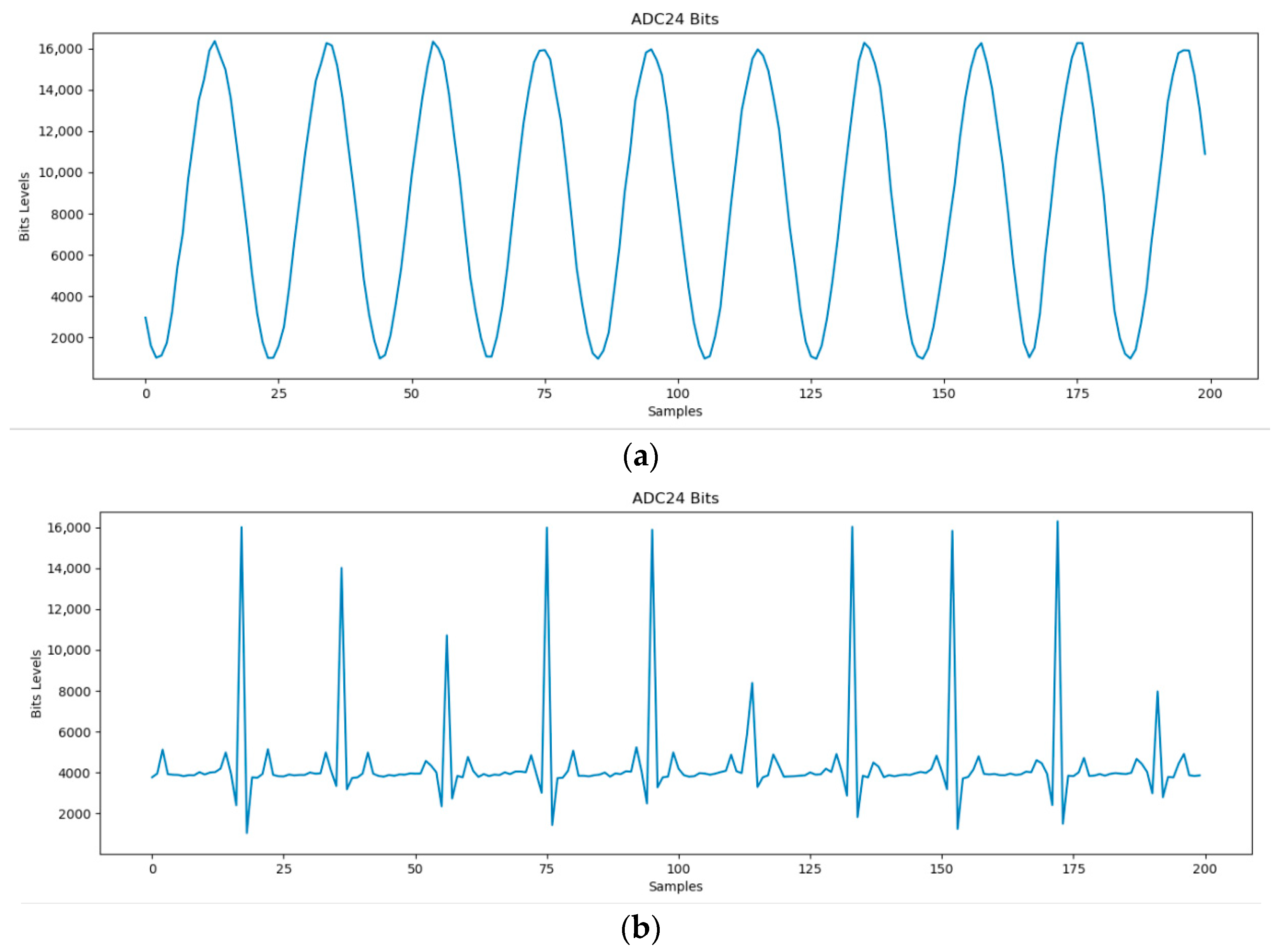
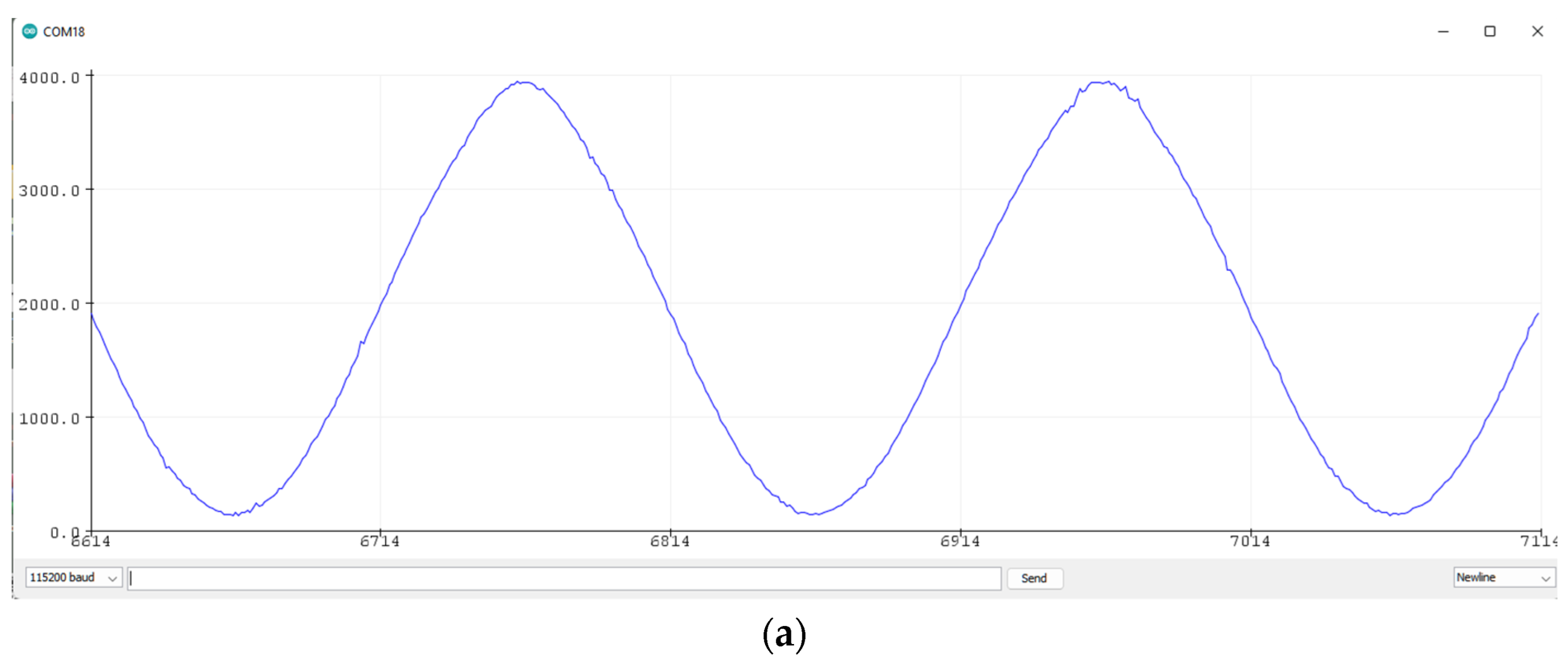
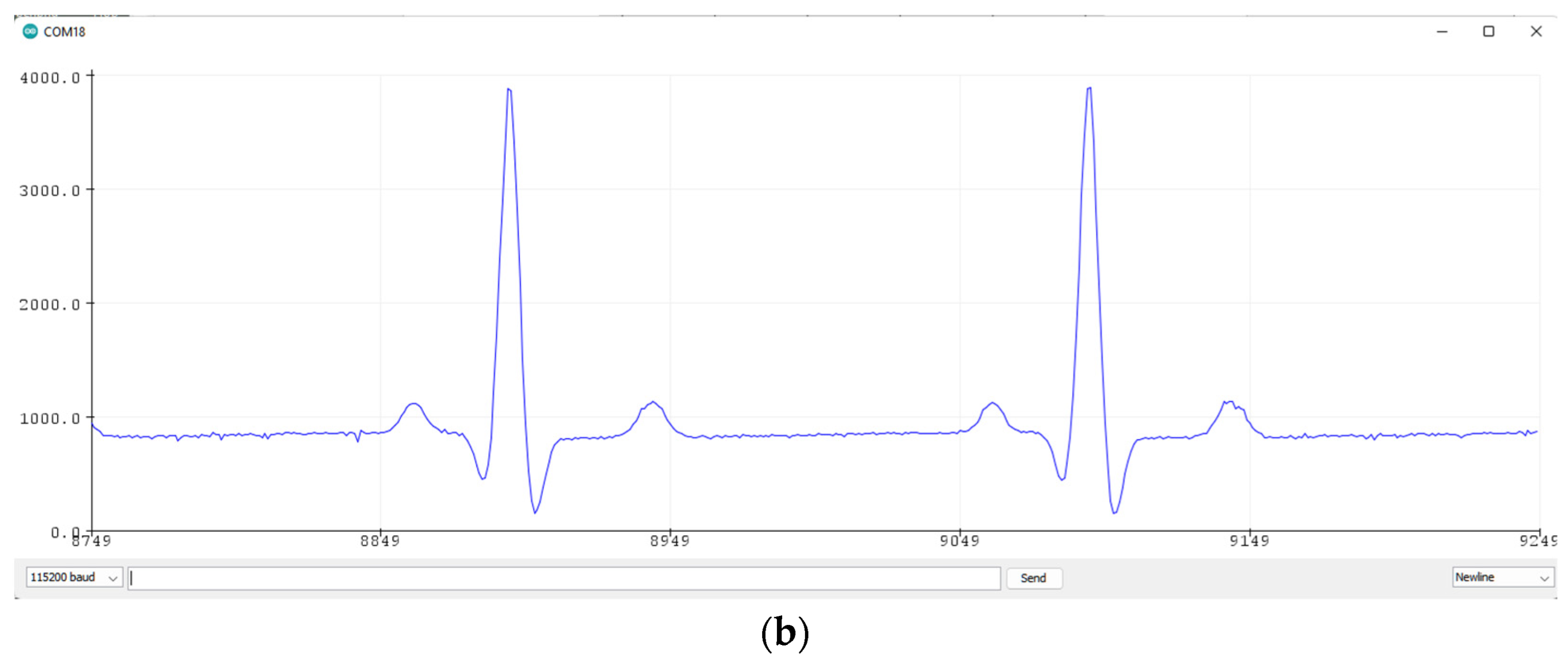
The ADC24 module test aimed to verify the correct operation of the ADS1256 24-bit analog-to-digital converter across its eight available input channels. As described previously, these channels are accessible through the acquisition card slots, allowing multiple devices to share the high-resolution converter. For the 24-bit acquisition stage, waveform sampling was performed at a standard sampling rate of up to 30 kSPS, consistent with the nominal maximum data rate specified by the manufacturer for single-ended operation. This configuration ensures adequate temporal resolution for low-frequency and biomedical signals while preserving the effective resolution of the converter. Communication with the ADS1256 was established using a dedicated Python routine, which enabled real-time data acquisition and visualization. Since the implementation supports reading one channel at a time, each input was tested sequentially by adjusting the channel selection parameters. All channels were successfully validated, confirming the correct functionality and configurability of the ADC24 module. For the experimental validation, a function generator was used to apply controlled analog signals directly to the analog input of the GPIO_tester card, which served as the interface to the ADC. The tests were repeated across all acquisition slots (1 to 6) to ensure consistent analog performance regardless of the physical position within the system. Two representative analog signals were applied. The first was a sinusoidal waveform with an amplitude of 4.8 V and a frequency of 200 Hz, configured to remain within the ADC operating range (0–5 V). In this case, a reference offset of 2.5 V was used to center the signal within the conversion range, allowing symmetrical visualization of both positive and negative waveform components. The second signal was a medical-pattern waveform simulating an electrocardiogram (ECG), with a peak-to-peak amplitude of 4.8 V and a frequency of 0.5 Hz between peaks. Due to its asymmetric profile, the reference offset was adjusted to 750 mV to prevent saturation and ensure proper visualization of all waveform features. Figure 21 presents representative output signals acquired during these tests, including the sinusoidal waveform on the top and the ECG-like trace on the bottom. The results demonstrate stable waveform reconstruction and correct handling of different signal profiles, supporting the suitability of the ADC24 module for high-resolution analog signal acquisition within the proposed proof-of-concept architecture.
The channel testing of the ADC24 module demonstrated consistent and reliable operation across all evaluated inputs and slots. All tested ADC channels successfully captured and accurately displayed both sinusoidal and electrocardiogram (ECG) signals, with no observed reading errors or waveform distortions. These results confirm the full functionality of the ADC24 across its inputs and validate the integrity of the distributed acquisition architecture implemented in the data-logger.
The ADS1256 operated flawlessly throughout all tests. All channels were successfully validated, with no errors, abnormalities, or significant noise detected during signal acquisition. These results demonstrate both the robustness of the design and the successful integration of the ADS1256 into the system.

4.6. ADC Test via ATSAM3X (12-Bit)

The validation of the 12-bit ADC followed the same methodology adopted for the 24-bit acquisition stage, using representative input signal profiles to assess functional performance. For the 12-bit acquisition stage implemented using the ATSAM3X microcontroller, waveform sampling was carried out at approximately 1 kSPS, a conservative rate compatible with stable serial communication, real-time visualization, and continuous acquisition under the proof-of-concept constraints. All evaluated channels successfully acquired and reproduced both sinusoidal and electrocardiogram-like signals within the specified operating range, demonstrating correct response to symmetric and low-frequency asymmetric waveforms. Data acquisition and visualization were performed using the Nexus.py application interfaced with the ATSAM3X microcontroller, enabling real-time signal monitoring and basic data recording. Throughout the experiments, the acquisition process remained stable, with no communication errors or operational instabilities observed. These results confirm the functional integrity of the 12-bit acquisition stage and its suitability for use within the scope of this proof-of-concept platform.

4.7. ADC Test via ATMEGA328 (10-Bit)

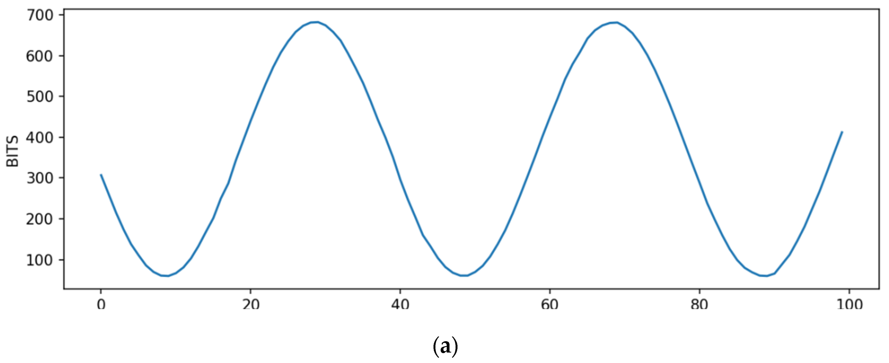
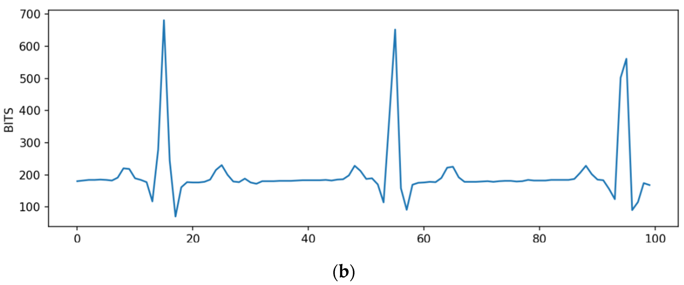
The validation procedure for the 10-bit ADC followed the same methodology adopted for the higher-resolution converters, using two representative input signals. For the 12-bit acquisition stage implemented using the ATMEGA microcontroller, waveform sampling was carried out at approximately 100 SPS, a standard AnalogoRead(). A sinusoidal waveform with an amplitude of 4.8 V and a frequency of 200 Hz was applied within the ADC operating range (0–5 V), with the reference offset (VCC/2) set to 2.5 V. In addition, an electrocardiogram-shaped waveform with a 4.8 V amplitude and a peak interval of 0.5 Hz was used to evaluate the system’s response to low-frequency, asymmetric biomedical signals. Data acquisition and visualization were performed using the Nexus.py application. Figure 22 presents representative output signals acquired with 10-bit resolution, including the sinusoidal waveform and the ECG-like signal. In both cases, the signals were correctly reconstructed, with all characteristic waveform features preserved throughout the tests. These results confirm the correct operation of the 10-bit acquisition stage within the scope of the proposed proof of concept.
The validation of the 10-bit ADC channels demonstrated reliable operation across all evaluated channel–slot combinations. For the 10-bit acquisition stage based on the ATMEGA328 microcontroller, waveform sampling was performed at approximately 1 kSPS, consistent with the ADC conversion time and reliable serial data throughput of the platform, and sufficient for the evaluation of low-frequency and event-based signals. All tested inputs successfully acquired and reproduced both sinusoidal and electrocardiogram-like signals, with no communication errors or operational failures observed under the tested conditions. The ATMEGA328 microcontroller operated consistently throughout the acquisition process, with both available analog channels functioning as expected. In addition, a second acquisition board was successfully exercised using the Nexus.py application, enabling device communication, channel reading, and real-time signal visualization. Although the software remains under development, its current functionality was sufficient to support the functional validation of the 10-bit acquisition stage within the scope of this proof-of-concept platform.

4.8. Test of External Connections via Return Bus

The analog channels available on the return bus were also experimentally validated. Although the return bus does not incorporate dedicated analog-to-digital converters, its primary function is to transport analog signals from the acquisition cards to an external readout point. For this evaluation, a GPIO_tester board was configured as the return card and connected to an external Arduino-based acquisition setup. The Arduino digitized the incoming signals at 10-bit resolution and transmitted the data to a host computer via USB for visualization and analysis. As the return bus operates as a shared analog pathway, a single slot configuration was sufficient for the test; however, all available analog channels on the bus were individually exercised. The acquired signals were processed and visualized on the host computer using the Arduino IDE plotting tools. Figure 23 presents representative waveforms transmitted through the return bus, including a sinusoidal signal and an electrocardiogram-shaped waveform. In both cases, the characteristic features of the original signals were preserved throughout transmission, indicating correct signal routing through the bus under the tested conditions. During the validation procedure, the return bus operated reliably, with all evaluated channels functioning as expected. No transmission interruptions or operational instabilities were observed, and the analog signals maintained their overall shape during transport. These results support the use of the return bus as an auxiliary interface for analog signal routing to external acquisition or processing systems within the scope of the proposed proof of concept.

5. Conclusions

This work presented the design, implementation, and experimental validation of Nexus, a modular multichannel data-logger conceived as a proof-of-concept platform for flexible and accessible scientific instrumentation. The system was developed through an integrated engineering process encompassing electronic design, mechanical fabrication, embedded firmware, and software integration. Rather than targeting a finalized commercial product, Nexus was intentionally conceived as a pilot platform to validate architectural concepts, modularity, and system-level integration under realistic laboratory conditions.
The experimental results demonstrate that the proposed architecture is functionally sound. All evaluated subsystems, including acquisition cards, backbone, motherboard, power supply, storage, and processing unit, operated as expected within the scope of the performed validation procedures. The successful integration of heterogeneous acquisition modules, multiple communication protocols, and a Raspberry Pi–based human–machine interface confirms the feasibility of the proposed modular approach and its suitability for exploratory and developmental applications.
From an electronic standpoint, the backbone and motherboard fulfilled their intended roles as interconnection and coordination layers, respectively, enabling reliable signal routing and communication between acquisition modules and the central processor. The use of multiple microcontrollers and ADC resolutions allowed functional validation of analog and digital acquisition paths, while the power subsystem ensured stable operation during prolonged laboratory tests. The Raspberry Pi CPU provided sufficient processing capability for data handling, visualization, and storage, highlighting the advantages of decoupling computational resources from the acquisition hardware.
The mechanical design supported the modular concept by ensuring proper alignment, secure card insertion, and ease of maintenance. The enclosure, card guides, and touchscreen integration proved adequate for repeated assembly and testing cycles, reinforcing the practicality of the proposed form factor for iterative development and future extensions.
On the software side, the development effort focused primarily on validation and system bring-up. A collection of test routines enabled structured evaluation of communication protocols and acquisition paths, while the Nexus.py application emerged as a preliminary control interface for data acquisition and visualization. Although still under active development, this software layer provided sufficient functionality to support the experimental validation of the platform and establishes a foundation for future expansion.
Overall, the results confirm that Nexus functions as a viable proof-of-concept for a modular, reprogrammable data-logger architecture. While extensive field deployment and long-term characterization were beyond the scope of this study, the performed tests demonstrate the platform’s capability to acquire, route, and store multichannel data in a controlled laboratory environment.
It is important to emphasize that Nexus was developed and validated as an engineering proof-of-concept platform intended to be operated by personnel trained in electronics, instrumentation, and data acquisition systems. Its use in regulated environments, such as hospitals or clinical facilities, would require specialized technical staff and compliance with applicable safety and certification standards. Therefore, the present implementation is not intended for direct clinical operation, but rather as a foundation for future developments toward more autonomous and user-friendly data acquisition systems.
Future work will focus on evolving Nexus into an open development platform, enabling broader community use and iterative improvement. Planned developments include enhanced firmware support for dynamic card identification and hot-swap management, expansion of the Nexus.py interface toward a modular and plugin-based architecture, and improved diagnostic and configuration tools. In addition, the integration of embedded data processing and artificial intelligence techniques such as anomaly detection, biosignal analysis, and edge-level decision support is envisioned as a long-term research direction. Through these efforts, Nexus is expected to be validated as a flexible experimental platform for research, education, and applied development in biomedical instrumentation, industrial monitoring, and related domains [39,40,41,42,43,44,45,46].

Author Contributions

Conceptualization: M.L.M.A., O.H.A.J. and J.P.P.d.C.; methodology: M.L.M.A., O.H.A.J. and J.P.P.d.C.; validation: M.L.M.A., O.H.A.J. and J.P.P.d.C.; investigation and simulation: M.L.M.A., O.H.A.J., M.G. and J.P.P.d.C.; writing—original draft preparation: M.L.M.A., O.H.A.J., M.G. and J.P.P.d.C. writing—review and editing: M.L.M.A., O.H.A.J., M.G. and J.P.P.d.C.; project administration: J.P.P.d.C.; funding acquisition: O.H.A.J., M.G. and J.P.P.d.C. All authors have read and agreed to the published version of the manuscript.

Funding

O.H.A.J. was funded by the Brazilian National Council for Scientific and Technological Development (CNPq), grant numbers 407531/2018-1, 303293/2020-9, 405385/2022-6, 405350/2022-8 and 406662/2022-3.

Data Availability Statement

Data is contained within the article.

Conflicts of Interest

The authors declare no conflicts of interest.

References

  1. Furgel, I.; Lemke, K. A Review of the Digital Tachograph System; Springer: Berlin/Heidelberg, Germany, 2006; pp. 69–94. [Google Scholar] [CrossRef]
  2. Lecuyer, C.; Brock, D.C. Makers of the Microchip; MIT Press: Cambridge, MA, USA, 2022. [Google Scholar]
  3. Zima, A.; Duprat, S.; Frangi, J.-P. Framework of a New Low-Cost Multipurpose Building Operation Datalogger Measurement Network. In Proceedings of the 2016 IEEE Intl Conference on Computational Science and Engineering (CSE) and IEEE Intl Conference on Embedded and Ubiquitous Computing (EUC) and 15th Intl Symposium on Distributed Computing and Applications for Business Engineering (DCABES), Paris, France, 24–26 August 2016. [Google Scholar] [CrossRef]
  4. Kim, H.J.; Byun, H.; Song, Y.B.; Shin, S.H.; Cho, S.; Pyeon, C.H.; Lee, B. Multi-channel fiber-optic temperature sensor system using an optical time-domain reflectometer. Results Phys. 2018, 11, 743–748. [Google Scholar] [CrossRef]
  5. Vancea, C.M.; Viman, L. Wireless Data logger for Thermal Validation Systems. In Proceedings of the 2011 IEEE 17th International Symposium for Design and Technology in Electronic Packaging (SIITME), Timisoara, Romania, 20–23 October 2011. [Google Scholar] [CrossRef]
  6. Kamrueng, C.; Kittiratsatcha, S.; Polmai, S. A Number of RC Pairs Consideration of Electrical Equivalent Circuit Model of Li-ion Battery. In Proceedings of the 2020 6th International Conference on Engineering, Applied Sciences and Technology (ICEAST), Chiang Mai, Thailand, 1–4 July 2020. [Google Scholar] [CrossRef]
  7. Jespers, P.G.; Murmann, B. Systematic Design of Analog CMOS Circuits: Using Pre-Computed Lookup Tables; Cambridge University Press: Cambridge, UK, 2018. [Google Scholar]
  8. Mulik, S.S.; Patange, A.D.; Jegadeeshwaran, R.; Pardeshi, S.S.; Rahegaonkar, A. Development and Experimental Assessment of a Fluid Flow Monitoring System Using Flow Sensor and Arduino Interface. In Innovative Design, Analysis and Development Practices in Aerospace and Automotive Engineering; Springer Nature: Berlin, Germany, 2021; pp. 115–122. [Google Scholar]
  9. Smith, K.; Amorim, M.; Marcic, S.; Reining, Z.; Ristow, N.; Miller, D.; Marzullo, T.C.; Serbe-Kamp, É.; Gage, G.J.; Leonhardt, A.; et al. Low-cost classroom and laboratory exercises for investigating both wave and event-related electroencephalogram potentials. J. Undergrad. Neurosci. Educ. 2024, 22, A197–A206. [Google Scholar] [CrossRef]
  10. Model. Available online: https://www.ni.com/pt-br/shop/model/usb-4431.html (accessed on 17 July 2023).
  11. Takahashi, H.; Hirano, K.; Yamada, K. Practical calibration method of airborne ultrasound measurement system by using acoustic calibrators. NOISE-CON Proc. 2023, 265, 2201–2207. [Google Scholar] [CrossRef]
  12. Watts, J.; Horoshenkov, K. Detecting defects in rising mains using the acoustic fluid velocity. Measurement 2025, 253, 117702. [Google Scholar] [CrossRef]
  13. Wu, X.; Song, J.; Duan, Z.; Wang, X.; Ding, W.; Wu, J.; Lu, S. Air gap flux density measurement of PMSLM based on TMR sensing external stray magnetic field and CNN-LSTM. Measurement 2024, 231, 114617. [Google Scholar] [CrossRef]
  14. Bartnes, C.; Ockernahl, A.; Dybvik, H.; Steinert, M. Promoting open research by adapting proprietary hardware to open-source software. In DS 118: Proceedings of NordDesign 2022; The Norwegian University of Science and Technology (NTNU): Trondheim, Norway, 2022. [Google Scholar] [CrossRef]
  15. Pearce, J.M. Economic Savings for Scientific Free and Open Source Technology: A Review. HardwareX 2020, 8, E00139. [Google Scholar] [CrossRef]
  16. Perdana, P.P.P.; Lingga, S.; Nusyirwan, D. Rancang Bangun Smart Book Calculator Berbasis Mikrokontroller Arduino uno Sebagai Inovasi Cerdas Untuk Memudahkan Siswa Menghitung guna Menuju Revolusi Industri 4.0 Design Build of Smart Book Calculator Based on Microcontroller Arduino uno as Intelligent Innovation to Easy Students to Calculate Towards Industrial Revolution 4.0. 2020, pp. 13–22. Available online: https://www.researchgate.net/publication/340492828_rancang_bangun_smart_book_calculator_berbasis_mikrokontroller_arduino_uno_sebagai_inovasi_cerdas_untuk_memudahkan_siswa_menghitung_guna_menuju_revolusi_industri_40_design_build_of_smart_book_calculato (accessed on 17 July 2023).
  17. Ortmeyer, C. A Modular Revolution. New Electron. 2020, 53, 20–21. [Google Scholar] [CrossRef]
  18. Pereira, R.I.; Dupont, I.M.; Carvalho, P.C.; Jucá, S.C. IoT embedded linux system based on Raspberry Pi applied to real-time cloud monitoring of a decentralized photovoltaic plant. Measurement 2018, 114, 286–297. [Google Scholar] [CrossRef]
  19. Pasquali, V.; D’Alessandro, G.; Gualtieri, R.; Leccese, F. A new data logger based on Raspberry-Pi for Arctic Notostraca locomotion investigations. Measurement 2017, 110, 249–256. [Google Scholar] [CrossRef]
  20. Cañete-Carmona, E.; Gallego-Martínez, J.J.; Yousef-Jiménez, L.; Ruiz-Flores, A.; Andrés Gersnoviez Moreno, J. An IoT barrel bung to monitor evolution wine elaborated under biological aging. Measurement 2022, 199, 111471. [Google Scholar] [CrossRef]
  21. Amorim, M.; Lima, J.G.; Nadia, N.; Afonso, J.A.; Lopes, S.F.; Carmo, J.P.P.D.; Hartmann, L.V.; Souto, C.R.; Salvadori, F.; Hideo, O. Open-Source Data Logger System for Real-Time Monitoring and Fault Detection in Bench Testing. Inventions 2024, 9, 120. [Google Scholar] [CrossRef]
  22. Gazziro, M.; Amorim, M.L.M.; Cavallari, M.R.; Carmo, J.P.; Júnior, O.H.A. Smart Personal Protective Equipment Hood Based on Dedicated Communication Protocol. Hardware 2025, 3, 8. [Google Scholar] [CrossRef]
  23. Mo Khin, J.M.; Oo, N.N. Real-Time Vehicle Tracking System Using Arduino, GPS, GSM and Web-Based Technologies. Int. J. Sci. Eng. Appl. 2018, 7, 433–436. [Google Scholar] [CrossRef]
  24. Achcha, V. Arduino Based Data Logger for Environmental Monitoring. SSRN Electron. J. 2021, 7, 3917850. [Google Scholar] [CrossRef]
  25. Kondaveeti, H.K.; Kumaravelu, N.K.; Vanambathina, S.D.; Mathe, S.E.; Vappangi, S. A Systematic Literature Review on Prototyping with Arduino: Applications, Challenges, Advantages, and Limitations. Comput. Sci. Rev. 2021, 40, 100364. [Google Scholar] [CrossRef]
  26. Linggarjati, J. Design and Prototyping of Temperature Monitoring System for Hydraulic Cylinder in Heavy Equipment using ESP32 with data logging and WiFi Connectivity. IOP Conf. Ser. Earth Environ. Sci. 2022, 998, 012042. [Google Scholar] [CrossRef]
  27. Keysight (n.d.). DAQ970A/DAQ973A Data Acquisition System PDF Asset Page|Keysight. Available online: https://www.keysight.com/us/en/assets/7018-06259/technical-overviews/5992-3168.pdf (accessed on 11 March 2024).
  28. Swagath, M.; Bailey, K. Integrating SPI and I2C Communication Protocols in a Controller Interface. Int. J. Creat. Res. Thoughts (IJCRT) 2024, 12. Available online: https://www.ijcrt.org/papers/IJCRT2407924.pdf (accessed on 11 March 2024).
  29. Chauhan, S.; Kumar, N. Estimating incident infrared radiation intensity on a horizontal surface. Measurement 2024, 231, 115250. [Google Scholar] [CrossRef]
  30. Powell, A. Democratizing production through open source knowledge: From open software to open hardware. Media Cult. Soc. 2012, 34, 691–708. [Google Scholar] [CrossRef]
  31. OSHWA.ORG. Brief History of Open Source Hardware Organizations and Definitions. 2022. Available online: https://oshwa.org/resources/brief-history-of-open-source-hardware-organizations-and-definitions/ (accessed on 12 March 2024).
  32. Niswar, M.; Nur, M.; Mappangara, I. A Low Cost Wearable Medical Device for Vital Signs Monitoring in Low-Resource Settings. Int. J. Electr. Comput. Eng. 2019, 9, 2321. [Google Scholar] [CrossRef]
  33. Pei, L.; Lo, M.T.; Tsao, J.; Chang, Y.-C.; Lin, C.; Ho, Y.-L. Correlations between the Signal Complexity of Cerebral and Cardiac Electrical Activity: A Multiscale Entropy Analysis. PLoS ONE 2014, 9, E87798–98. [Google Scholar] [CrossRef]
  34. Vocabulary.com. (n.d.). Nexus—Definition, Meaning & Synonyms. Available online: https://www.vocabulary.com/dictionary/nexus (accessed on 18 January 2026).
  35. Anacona, P.I.; Luján, J.P.; Azócar, G.; Mazzorana, B.; Medina, K.; Durán, G.; Rojas, I.; Loarte, E. Arduino Data loggers: A Helping Hand in Physical Geography. Geogr. J. 2022, 189, 314–328. [Google Scholar] [CrossRef]
  36. Thonny.org. Thonny, Python IDE for Beginners. 2018. Available online: https://thonny.org/ (accessed on 18 January 2026).
  37. Codewith.mu. (n.d.). Code with Mu. Available online: https://codewith.mu/ (accessed on 18 January 2026).
  38. Amorim, M.L.M.; Ginja, G.A.; Carmo, J.P.; Moreira, M.M.A.; Siqueira, A.A.G.; Afonso, J.A. Low-Cost/High-Precision Smart Power Supply for Data Loggers. Energies 2022, 16, 278. [Google Scholar] [CrossRef]
  39. Junior, O.H.A.; Bretas, A.S.; Leborgne, R.C. Methodology for Calculation and Management for Indicators of Power Quality Energy. IEEE Lat. Am. Trans. 2015, 13, 2217–2224. [Google Scholar] [CrossRef]
  40. Diaz, V.S.; Cantane, D.A.; Santos, A.Q.O.; Ando Junior, O.H. Comparative Analysis of Degradation Assessment of Battery Energy Storage Systems in PV Smoothing Application. Energies 2021, 14, 3600. [Google Scholar] [CrossRef]
  41. Watanabe, R.B.; Ando Junior, O.H.; Leandro, P.G.M.; Salvadori, F.; Beck, M.F.; Pereira, K.; Brandt, M.H.M.; de Oliveira, F.M. Implementation of the Bio-Inspired Metaheuristic Firefly Algorithm (FA) Applied to Maximum Power Point Tracking of Photovoltaic Systems. Energies 2022, 15, 5338. [Google Scholar] [CrossRef]
  42. Torres, N.N.S.; Lima, J.G.; Maciel, J.N.; Gazziro, M.; Filho, A.C.L.; Souto, C.R.; Salvadori, F.; Ando Junior, O.H. Non-Invasive Techniques for Monitoring and Fault Detection in Internal Combustion Engines: A Systematic Review. Energies 2024, 17, 6164. [Google Scholar] [CrossRef]
  43. Villarim, M.R.; Villarim, A.W.R.; Gazziro, M.; Cavallari, M.R.; Belfort, D.R.; Ando Junior, O.H. Computational Tool for Curve Smoothing Methods Analysis and Surface Plasmon Resonance Biosensor Characterization. Inventions 2025, 10, 31. [Google Scholar] [CrossRef]
  44. de Lira, E.R.; da Silva, E.A.; Degiorgi, S.V.B.; do Carmo, J.P.P.; Ando Junior, O.H. Design and Performance Analysis of MPPT Algorithms Applied to Multistring Thermoelectric Generator Arrays Under Multiple Thermal Gradients. Energies 2025, 18, 6613. [Google Scholar] [CrossRef]
  45. Ando Junior, O.H.; Silva, E.A.d.; Lira, E.R.d.; Degiorgi, S.V.B.; Carmo, J.P.P.d. Comparative Analysis and Integrated Methodology for the Electrical Design and Performance Evaluation of Thermoelectric Generators (TEGs) in Energy Harvesting Applications. Energies 2024, 17, 5176. [Google Scholar] [CrossRef]
  46. Amorim, M.L.M.; Ginja, G.A.; Moreira, M.d.M.A.C.; Ando Junior, O.H.; Siqueira, A.A.G.; Monteiro, V.; Afonso, J.A.; Carmo, J.P.P.d.; Afonso, J.L. Development and Evaluation of a Piezoelectret Insole for Energy Harvesting Applications. Electronics 2025, 14, 4254. [Google Scholar] [CrossRef]
Figure 1. Presents a connection-oriented architectural diagram of the Nexus system.
Automation 07 00025 g001
Figure 2. Simplified view of the path followed by the captured signal.
Automation 07 00025 g002
Figure 3. Technical drawings of the Nexus with main views: (a) side, (b) front, (c) bottom, and (d) isometric.
Automation 07 00025 g003aAutomation 07 00025 g003b
Figure 4. Simplified diagram of communication between the motherboard and the CPU, where the CPU’s only connection is through the motherboard.
Automation 07 00025 g004
Figure 5. Detailed view of the ADC circuit: (a) analog inputs, (b) input voltage, (c) ADS1256, (d) SPI output to the CPU.
Automation 07 00025 g005
Figure 6. Block diagram of Auxiliary Circuit 1, highlighting the ATMEGA328-based analog acquisition, communication interfaces, and control functions. Items (a,b) show the auxiliary analog inputs and the ATMEGA328. Item (c) is the ATMEGA328, Items (d,e) depict the I2C interface and (f) configurable selector. Items (g,h) present the UART2 interface, and (i) routing selector. Item (j) shows the relay-based UART switching. Item (k) is the remote shutdown pin. Item (l) indicates the USB link to the CPU, and item (m) the auxiliary power-management trigger signal.
Automation 07 00025 g006
Figure 7. Diagram of Auxiliary Circuit 2 based on the ATSAM3X microcontroller: (a) analog input channels AN10–AN19; (b) analog signal domain prior to digital processing; (c) ATSAM3X microcontroller; (d) UART serial communication interface; (e) configurable selector for TX/RX signal routing; (f) jumper for UART signal mismatch correction; (g) I2C signal input to the ATSAM3X; (h) I2C bus lines to external peripherals; (i) jumper for I2C signal mismatch correction; (j) USB communication interface with the system infrastructure; (k) auxiliary control signal for remote power management triggering.
Automation 07 00025 g007
Figure 8. Diagram of direct digital interfaces between the CPU and the motherboard: (a,b) UART serial communication lines; (c) configurable selector for UART; (d,e) I2C input signal; (f) onboard jumper for signal mismatch correction; (g,h) first Serial Peripheral Interface (SPI0); (i) corresponding SPI0 input pins on the CPU; (j,k) second Serial Peripheral Interface (SPI1); (l) corresponding SPI1 input pins on the CPU; (m) dedicated control signal for remote system shutdown via the power management subsystem.
Automation 07 00025 g008
Figure 9. Presents the I/O pin assignments for each acquisition card, organized by processing unit. Pins (a,e) correspond to the ATSAM3X, (b,f) to the ATMEGA328, (c,g) to the Raspberry Pi 4B, and (d,h) to the mainboard prototyping area (not implemented). The figure details the assignments for Cards 1–6, illustrating a consistent slot structure with independent addressing and control.
Automation 07 00025 g009
Figure 10. Shows the functional segmentation of the custom motherboard: (a) analog input stage, (b) digital communication inputs, (c) exclusive acquisition inputs, (d) expansion headers, (e) Raspberry Pi interface and fan, (f) ATSAM3X subsystem, (g) ATmega328 auxiliary controller, (h) USB hub, (i) UART to the power supply, (j) power-enable circuitry, and (k) main power input with onboard regulator.
Automation 07 00025 g010
Figure 11. Simplified layout of the return bus path.
Automation 07 00025 g011
Figure 12. Backbone board of the Nexus data logger. Top picture: front side showing seven 120-pin PCI slots, including six acquisition card input slots (Slots 1–6) and one dedicated output slot for the return bus (Slot 7), located at the far right. Bottom picture: rear side showing the power input connectors (a), analog signal connector (b), six USB ports for direct card communication (c), dedicated pin connectors for acquisition cards 1–2 (d), 3–4 (e), and 5–6 (f), a shared digital signal connector (g), and separated digital (GND-D) and analog (GND-A) ground connections (h,i).
Automation 07 00025 g012
Figure 13. GPIO_tester card: white plastic cover secured with two screws, right side showing the internal area (a), left side of the panel showing the external area (b), contact pins (c), and PCI bus integrated into the board at (d).
Automation 07 00025 g013
Figure 14. Shows the front of the data-logger in operation, with the screen displaying the system’s file manager, demonstrating the proper functioning of the graphical interface.
Automation 07 00025 g014
Figure 15. USB communication architecture of the Nexus system, illustrating the connection between acquisition card microcontrollers and the central processing unit through an internal USB hub.
Automation 07 00025 g015
Figure 16. I2C communication diagram.
Automation 07 00025 g016
Figure 17. SPI communication diagram, showing the ADC with a dedicated SPI channel.
Automation 07 00025 g017
Figure 18. UART communication diagram showing the MCUs and the CPU.
Automation 07 00025 g018
Figure 19. Four types of I2C communication protocol tests.
Automation 07 00025 g019
Figure 20. SPI signal path.
Automation 07 00025 g020
Figure 21. ADC24-bit test results: (a) sine wave; (b) medical electrocardiogram waveform.
Automation 07 00025 g021
Figure 22. Test of the 10-bit ADC: (a) sine wave; (b) medical electrocardiogram waveform.
Automation 07 00025 g022aAutomation 07 00025 g022b
Figure 23. Test of the return bus: (a) sinusoidal waveform and (b) medical electrocardiogram waveform.
Automation 07 00025 g023aAutomation 07 00025 g023b
Table 1. I2C results with MCU II.
Signal Chain I2C:
Automation 07 00025 i001
SlotMCUSensorAddr.ETRDataI2C ChainSwapErro
1ATMEGA328MLX90614ES0 × 5A1.48 kHzAmbient = 27.2
Device = 31.8
YESYESNO
2ATMEGA328MLX90614ES0 × 5A1.50 kHzAmbient = 27.0
Device = 32.1
YESYESNO
3ATMEGA328MLX90614ES0 × 5A1.48 kHzAmbient = 27.2
Device = 32.3
YESYESNO
4ATMEGA328MLX90614ES0 × 5A1.48 kHzAmbient = 27.1
Device = 32.4
YESYESNO
5ATMEGA328MLX90614ES0 × 5A1.50 kHzAmbient = 26.7
Device = 31.8
YESYESNO
6ATMEGA328MLX90614ES0 × 5A1.48 kHzAmbient = 26.8
Device = 31.2
YESYESNO
1ATMEGA328SI70210 × 402.07 kHzRelative humidity
= 28.33%
YESYESNO
2ATMEGA328SI70210 × 402.03 kHzRelative humidity
= 28.33%
YESYESNO
3ATMEGA328SI70210 × 402.05 kHzRelative humidity
= 28.33%
YESYESNO
4ATMEGA328SI70210 × 402.07 kHzRelative humidity
= 28.33%
YESYESNO
5ATMEGA328SI70210 × 402.04 kHzRelative humidity
= 28.33%
YESYESNO
6ATMEGA328SI70210 × 402.07 kHzRelative humidity
= 28.33%
YESYESNO
Table 2. I2C results with MCU I.
Signal Chain I2C:
Automation 07 00025 i002
SlotMCUSensorAddr.ETRDataI2C ChainSwapErro
1ATSAM3XMLX90614ES0 × 5A32 HzAmbient = 28.3
Device = 31.2
YESYESNO
2ATSAM3XMLX90614ES0 × 5A32 HzAmbient = 28.0
Device = 32.3
YESYESNO
3ATSAM3XMLX90614ES0 × 5A32 HzAmbient = 27.9
Device = 32.2
YESYESNO
4ATSAM3XMLX90614ES0 × 5A32 HzAmbient = 28.3
Device = 32.5
YESYESNO
5ATSAM3XMLX90614ES0 × 5A32 HzAmbient = 28.3
Device = 31.7
YESYESNO
6ATSAM3XMLX90614ES0 × 5A32 HzAmbient = 28.5
Device = 31.1
YESYESNO
1ATSAM3XSI70210 × 4028 HzRelative humidity
= 28.33%
YESYESNO
2ATSAM3XSI70210 × 4028 HzRelative humidity
= 28.33%
YESYESNO
3ATSAM3XSI70210 × 4028 HzRelative humidity
= 28.33%
YESYESNO
4ATSAM3XSI70210 × 4028 HzRelative humidity
= 28.33%
YESYESNO
5ATSAM3XSI70210 × 4028 HzRelative humidity
= 28.33%
YESYESNO
6ATSAM3XSI70210 × 4028 HzRelative humidity
= 28.33%
YESYESNO
Table 3. I2C results with the return bus and ESP32 Thing+.
Signal Chain I2C:
Automation 07 00025 i003
SlotMCUSensorAddr.ETRDataI2C ChainSwapErro
1ESP32Thing+MLX90614ES0 × 5A1.85 kHzAmbient = 27.5
Device = 28.3
YESYESNO
2ESP32Thing+MLX90614ES0 × 5A1.82 kHzAmbient = 27.2
Device = 28.7
YESYESNO
3ESP32Thing+MLX90614ES0 × 5A1.80 kHzAmbient = 27.4
Device = 28.4
YESYESNO
4ESP32Thing+MLX90614ES0 × 5A1.85 kHzAmbient = 27.1
Device = 28.7
YESYESNO
5ESP32Thing+MLX90614ES0 × 5A1.85 kHzAmbient = 26.6
Device = 28.3
YESYESNO
6ESP32Thing+MLX90614ES0 × 5A1.82 kHzAmbient = 26.5
Device = 28.6
YESYESNO
1ESP32Thing+SI70210 × 402.89 kHzRelative humidity
= 28.33%
YESYESNO
2ESP32Thing+SI70210 × 402.87 kHzRelative humidity
= 28.33%
YESYESNO
3ESP32Thing+SI70210 × 402.89 kHzRelative humidity
= 28.33%
YESYESNO
4ESP32Thing+SI70210 × 402.89 kHzRelative humidity
= 28.33%
YESYESNO
5ESP32Thing+SI70210 × 402.87 kHzRelative humidity
= 28.33%
YESYESNO
6ESP32Thing+SI70210 × 402.89 kHzRelative humidity
= 28.33%
YESYESNO
Table 4. I2C results directly on the CPU (Raspberry Pi).
Signal Chain I2C:
Automation 07 00025 i004
SlotMCUSensorAddr.ETRDataI2C ChainSwapErro
1RaspberryPiMLX90614ES0 × 5A1.85 kHzAmbient = 27.1
Device = 27.6
YESNONO
2RaspberryPiMLX90614ES0 × 5A1.82 kHzAmbient = 27.3
Device = 27.2
YESNONO
3RaspberryPiMLX90614ES0 × 5A1.80 kHzAmbient = 27.2
Device = 27.8
YESNONO
4RaspberryPiMLX90614ES0 × 5A1.85 kHzAmbient = 27.2
Device = 27.2
YESNONO
5RaspberryPiMLX90614ES0 × 5A1.85 kHzAmbient = 27.5
Device = 28.1
YESNONO
6RaspberryPiMLX90614ES0 × 5A1.82 kHzAmbient = 26.8
Device = 27.9
YESNONO
Table 5. Results of SPI tests on the CPU.
Signal Chain SPI
Automation 07 00025 i005
SlotMCUWritingReadingValueSwapErro
1RaspberryPi50.25 Mbps56.18 Mbps32 bitsNONO
2RaspberryPi50.18 Mbps56.32 Mbps32 bitsNONO
3RaspberryPi50.06 Mbps56.15 Mbps32 bitsNONO
4RaspberryPi50.20 Mbps55.75 Mbps32 bitsNONO
5RaspberryPi50.23 Mbps55.18 Mbps32 bitsNONO
6RaspberryPi50.20 Mbps56.12 Mbps32 bitsNONO
Table 6. Results of SPI tests on the ESP32 Thing+.
Signal ChainSPI
Automation 07 00025 i006
SlotMCUWritingReadingValueSwapErro
1ESP32Thing+38.20 Mbps40.35 Mbps32 bitsNONO
2ESP32Thing+36.42 Mbps42.16 Mbps32 bitsNONO
3ESP32Thing+36.80 Mbps40.62 Mbps32 bitsNONO
4ESP32Thing+38.06 Mbps41.50 Mbps32 bitsNONO
5ESP32Thing+38.17 Mbps42.44 Mbps32 bitsNONO
6ESP32Thing+35.89 Mbps40.82 Mbps32 bitsNONO
Table 7. Ideal transmission values of Baud Rate versus Bits in characters using the equation above.
Baud Rate10 Bits (4 Characters)16 Bits (5 Characters)24 Bits (8 Characters)
9600240192120
115,200288023041440
230,400576046082880
500,00012,50010,0006250
Table 8. USB transmission speed test in Baud Rate between the card and the CPU.
Signal Chain USB:
Automation 07 00025 i007
SlotReadingBaud Rate: 9600Baud Rate 115,200Baud Rate 230,400Baud Rate 500,000
10 Bits16 Bits24 Bits10 Bits16 Bits24 Bits10 Bits16 Bits24 Bits10 Bits16 Bits24 Bits
1LPS19213796196016801176370531762221426439043329
BAUD76806850768078,40084,00094,080148,200158,800177,680170,560195,200266,320
ERRONONONONONONONONONONONONO
2LPS19313896196116801177370131732223426539083326
BAUD77206900768078,44084,00094,160148,040158,650177,840170,600195,400266,080
ERRONONONONONONONONONONONONO
3LPS19113896196016801175370631762222426039083329
BAUD76406900768078,40084,00094,000148,240158,800177,760170,400195,700266,320
ERRONONONONONONONONONONONONO
4LPS19213796196016811176370131762221426439043326
BAUD76806850768078,40084,05094,080148,040158,800177,680170,560195,200266,080
ERRONONONONONONONONONONONONO
5LPS19213796196116801176370531722222426039083326
BAUD76806850768078,44084,00094,080148,200158,600177,760170,400195,700266,080
ERRONONONONONONONONONONONONO
6LPS19313896196016801175370231732223426439083326
BAUD77206900768078,40084,00094,000148,080158,650177,840170,560195,700266,080
ERRONONONONONONONONONONONONO
Disclaimer/Publisher’s Note: The statements, opinions and data contained in all publications are solely those of the individual author(s) and contributor(s) and not of MDPI and/or the editor(s). MDPI and/or the editor(s) disclaim responsibility for any injury to people or property resulting from any ideas, methods, instructions or products referred to in the content.