


Abstract
With parylene coatings, conventional layer thickness measurement methods such as gravimetry, reflectometry, and cross-sectional microscopy are performed post-process and do not allow real-time monitoring or control. This paper presents a novel in situ measurement method based on the capacitance change in interdigitated copper electrodes fabricated on a printed circuit board (PCB). As parylene deposits on this sensor, the effective permittivity above the electrodes increases from (vacuum) to (parylene), causing a measurable capacitance change. Finite element simulations were performed to model the relationship between layer thickness and sensor capacitance. Experimental validation with parylene C and F-VT4 demonstrated good agreement between simulation and measurement. Four consecutive parylene C runs with 60 g raw material showed reproducible capacitance increases of 49–53 pF, corresponding to layer thicknesses of 20–25 µm, verified by cross-sectional microscopy. Two coating runs were performed with parylene F-VT4 with target layer thicknesses of 2.5 µm and 5 µm. They show particularly good agreement with the simulation. The proposed method enables real-time process monitoring and provides a foundation for closed-loop control of parylene CVD processes.
1. Introduction
Parylene [poly(p-xylylene)] is a high-performance coating material, which is coated in a chemical vapor deposition (CVD) process. It is optically transparent, chemically inert, has high dielectric strength and can coat almost any surface regardless of its material or geometry. Even sharp edges or narrow gaps are covered pinhole-free. It is used among other applications in medicine as a biocompatible coating [1] or in electronics as a dielectric and bonding material [2]. For the coating process, the raw material is in powder form. This powder is first vaporized in a vacuum at 100–200 °C and then monomerized above 600 °C in a pyrolysis process. The monomers settle on the substrate surfaces at approximately room temperature and polymerize there [3]. The vaporization of the parylene powder causes a slight increase in pressure within the vacuum chamber. Once the powder is used up and no further coating processes are taking place, the pressure drops. That is the termination criterion for the coating process.
The layer thickness during parylene CVD is usually defined by the added weight of parylene raw material. However, the actual deposited thickness depends on numerous process parameters, including process pressure, evaporation and pyrolysis temperatures, substrate temperature, chamber geometry, and substrate surface properties [4]. For example, the evaporation temperature influences the mass flow into the reactor. Furthermore, process gases can modify the layer growth rate. Typically, the coated device operates at room temperature. If a part is actively cooled, the deposition rate and the so-called sticking coefficient increase [5]. Liu et al. demonstrate a method for precisely controlling the deposition rate of parylene by adjusting the chamber pressure [6].
To check the quality of parylene coating, the layer thickness must be measured. After the coating process, this can be done, for example, gravimetrically, by reflectometry, or by cross-section images. These methods cannot be used during the coating (in situ), which would be necessary to control the process in a closed loop. An application that affords well-controlled growth is ultra-thin parylene substrates (e.g., used in solar cells) [7].
Ga-Yeon Lee et al. present a potential in situ measurement method [8]. The resonance frequency of a quartz crystal is continuously measured (QCM method). As the layer thickness increases, the resonance frequency decreases. Sumotomo et al. describe an endpoint measurement method as a termination criterion once the coating thickness is sufficient during the parylene process [9]. They use a heat source and a temperature sensor that are thermally separated by a small gap. Heat conduction in the vacuum during coating is negligible. As soon as parylene covers the gap, the temperature at the sensor rises sharply. This signals the termination of the process. Here, the target layer thickness is defined by the gap width. Taylor and Welber irradiate a metal plate with a He-Ne laser during the coating process to determine the quality of the parylene [10]. However, this quality check is highly dependent on factors such as the parylene type or the pyrolysis temperature.
This paper presents a capacitive in situ layer thickness measurement method for parylene CVD. The capacitive method is also used, for example, in humidity sensors [11]. In humidity sensors, the measurement principle takes advantage of the permittivity difference between air and water. Overall, the concentration of a substance in the immediate vicinity of a conductor structure consisting of two electrodes impacts the measured capacitance between these two electrodes. Touchscreens also use a capacitive sensing method. In this case, however, it is the distance between the electrodes that changes, not the material.
Compared to the QCM method, the capacitive approach offers a lower cost. A typical QCM resonator costs $65 (May 2026) [12], while the capacitive sensor elements used cost less than $1. Unlike thermal endpoint detection, which provides only a binary stop signal at a predetermined thickness [9], the capacitive method delivers a continuous process curve enabling real-time monitoring. In contrast to laser-based methods [10], no optical access to the chamber is required, and the measurement is independent of pyrolysis temperature.
The main limitation of the capacitive approach is that the sensor measures thickness at its own location rather than directly on the workpiece, and calibration is required for each parylene type due to different permittivities. This in situ method helps to better understand coating processes and—for future applications—it gives a control parameter during coating. The objectives are threefold: (1) to design and characterize a low-cost, single-use sensor element suitable for industrial application, (2) to establish the relationship between capacitance change and layer thickness through finite element simulation, and (3) to validate the method experimentally with parylene C and F-VT4 coatings.
2. Measurement Method
In this paper, a printed circuit board (PCB) consisting of two electrodes is designed, simulated, and tested to conduct capacitive measurement of the coating thickness of parylene inside the vacuum chamber. In addition, a capacitance measurement unit is being developed. During measurement, it is located outside the system and connected to the sensor element via coaxial cables. The measurements are compared with electric field simulations. The physics behind the capacitive measurement method, the design parameters and testing process are described in this chapter.
As shown in Table 1, parylene has a relative permittivity between 2.1 and 3.2, depending on the chemical type and the frequency. In the data sheet [13], the relative permittivity of parylene N, C, D, F-VT4 and F-AF4 (these abbreviations refer to the substituents in the respective chemical monomers) as a dependence on frequency is indicated as follows:
Table 1.
Relative permittivity of parylene N, C, D, F-VT4 and F-AF4.
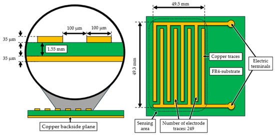
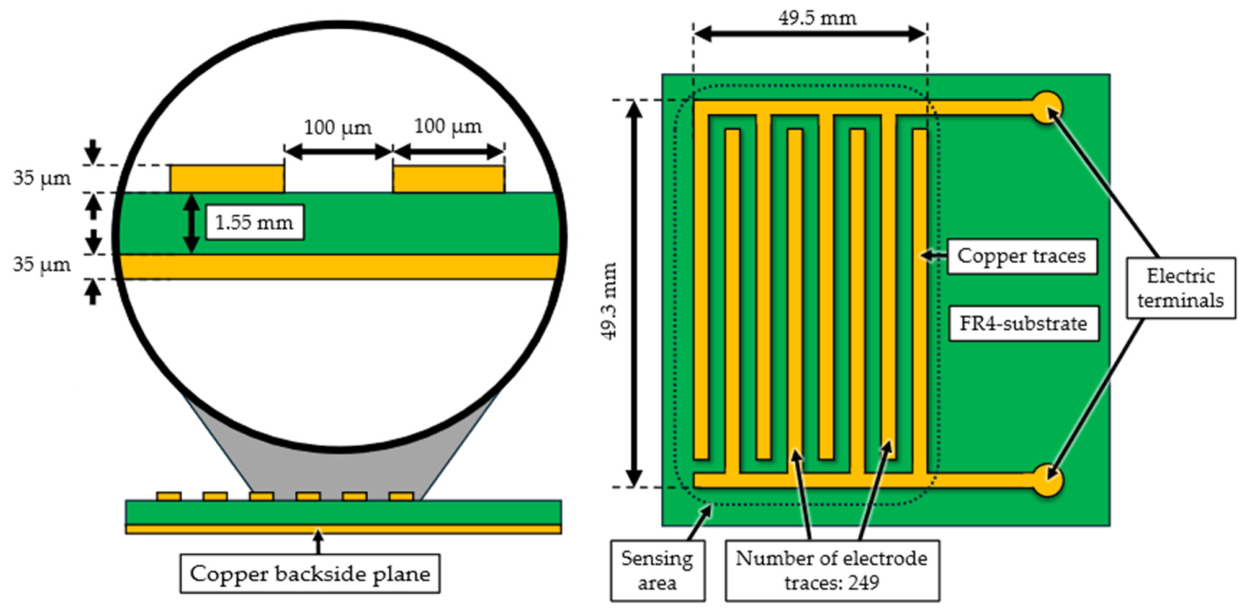
Parylene provides a significant difference compared to the permittivity of air or vacuum (). The sensor element should be designed in such a way that the capacitance between two electrodes changes as much as possible when parylene covers the electrodes. A similar principle is known from humidity sensors [14]. The high sensitivity of the parylene sensor is achieved by interdigitated copper electrodes on a printed circuit board (PCB), as depicted in Figure 1. The backside of the PCB is realized as a copper plate covering the entire sensor area to provide a well-defined reference potential and shielding for the electric field. PCBs are particularly well-suited for this application due to their fine structurability and low prices. With a PCB, the sensor elements can be designed as single-use products. They do not require time-consuming cleaning after a coating. As a substrate, FR4 material with a relative permittivity between 4.4 and 4.6 was selected. It features copper traces with a thickness of 35 µm and a width of 100 µm. The 249 traces are each 100 µm apart. The total measuring area is approximately 2440 mm2.
Figure 1.
Schematic figure of the interdigitated PCB sensor element, including geometric and material properties. (Green: FR4 material; Orange: copper).
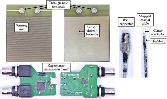
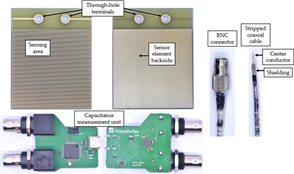
A realistic representation of the sensor element and the capacitance measurement unit is shown in Figure 2. Both elements are shown from the front and rear. For in situ measurement, two stripped coaxial (coax) cables are routed inside the vacuum chamber to the rear of the sensor, where they are connected to the interdigitated structure via through-hole terminals. Both coax cables are linked to the outside via BNC connectors in a vacuum-sealed flange. On the outside, the cables are likewise connected to the capacitance measuring unit via BNC connectors. The measurement unit is customized for this application and measures capacitance at f = 10 kHz. Inside the chamber, the cables and connectors continue to become coated with parylene with each run and must be replaced every 300 µm of deposited coating layer thickness. As an illustrative example, Figure 2 shows the ends of a coax cable coated with parylene. The shielding of the coax cables is soldered to the backside of the sensor element, setting the copper plane to ground potential. Thus, the sensor element is independent of charges or metallic surfaces on its rear side.
Figure 2.
Photo of the real PCB sensor element and the capacitance measurement unit.
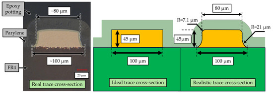
To compare the quality of a run with the in situ measurements, the sensor element after the run is potted in EpoThin 2 epoxy, ground, and examined under a Keyence (Frankfurt am Main, Germany) VHX-2000 optical microscope. Such a cross-section of a copper trace with parylene coating is shown in Figure 3. The epoxy provides mechanical stability and enables a grinding process that is as non-destructive as possible. The parylene layer is easy to see in the microscope image. The micrograph also shows that the cross-section of a trace is not rectangular, as assumed in the schematic representation in Figure 1. Instead, due to the etching process during PCB manufacturing, the copper trace has a typical rounding with a radius of 6 to 8 µm at the two exposed edges. This was determined by measuring the optical distances in the microscope images. On the FR4-side, there is a tip with a radius of 15 to 25 µm. Figure 3 compares this copper trace cross-section with a schematic representation of the ideal rectangular shape and the realistic shape. When simulating the capacitance change in the sensor element in Ansys (Canonsburg, USA) Maxwell electrostatic due to parylene, the realistic cross-section is used to reduce errors.
Figure 3.
Cross-section of a sensor element with the etched copper traces and parylene coating. (Green: FR4 material; Orange: copper; Ash grey: Parylene).
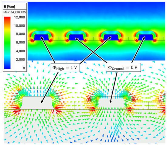
When calculating the change in capacitance caused by the deposition of parylene, the electric fields are particularly relevant. The electric field around interdigitated electrodes with a realistic shape is shown in Figure 4. Here, the sensor is coated with a 20 µm layer of parylene. There is a potential difference of 1 V between each pair of adjacent traces. It is remarkable that the electric field only reaches high values in the immediate surroundings of the electrode. Just 150 µm away, the electric field is already significantly below 10% of the maximum. This illustration shows that the copper plate on the back of the sensor element has no significant influence on the electric field. Therefore, the capacitance of the element reacts sensitively to changes in the parylene coating. Ansys Maxwell 2D is used to simulate the electric fields.
Figure 4.
Cross-section of the traces with a 20 µm parylene layer displaying the electric field’s magnitude and vectors around the electrodes in Ansys Maxwell 2D.
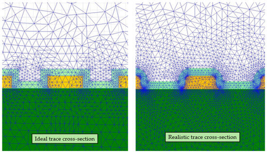
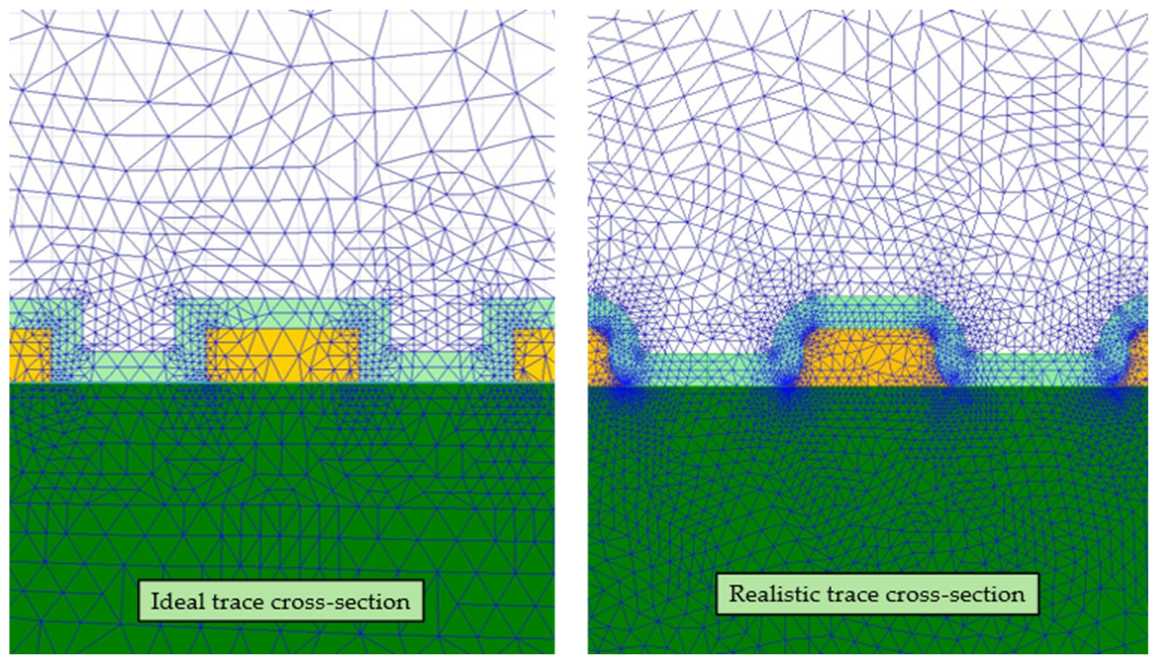
The mesh configuration for this simulation is shown in Figure 5. The average element size in the immediate vicinity of the parylene–copper interface in the ideal shape simulation is 35 µm2. In the simulation of the realistic shape, the average element size in the interface vicinity is approximately 8 µm2. Simulations showed that the rounding radii at the lower sharp corners of the realistic geometry were not significant within a range of up to 50 nm. Therefore, they were assumed to be perfectly sharp in the simulations.
Figure 5.
Meshing of the ideal and realistic trace cross-section in Ansys Maxwell 2D. (Mesh triangles in blue).
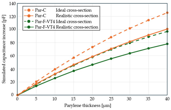
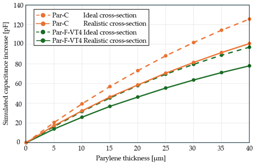
This paper focuses on parylene types C and F-VT4. These two types differ greatly in their relative permittivity ([f = 1 kHz] = 2.98 and [f = 10 kHz] = 2.5). Here, the parylene C data sheet specification for 1 kHz is used, as this frequency is closest to the actual measurement frequency of 10 kHz. Figure 6 shows the simulated capacitance increase for the two types of parylene as a function of layer thickness. A distinction is also made here between the results of the ideal and realistic cross-sections. However, the ideal cross-section no longer plays a role in later considerations. The simulated base capacitance of the ideal sensor element is . In the realistic cross-section, the base capacitance is . For layer thickness measurement, the increase in capacitance is interesting. Therefore, not the total capacitance but the increase due to the parylene layer is considered. The increase in capacitance at the realistic cross-section is generally lower than the increase in capacitance at the ideal cross-section. At the bottom side with spiky edges, the electric field is partly located inside the FR4 substrate, which does not change the permittivity during the coating process.
Figure 6.
Simulated capacitance increase in the sensor element in relation to the parylene thickness. The plot shows a comparison between the ideal and realistic cross-sections for the parylene types C and F-VT4.
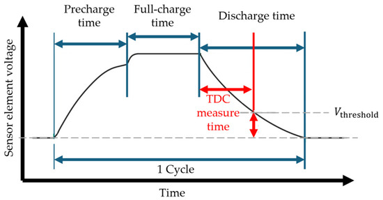
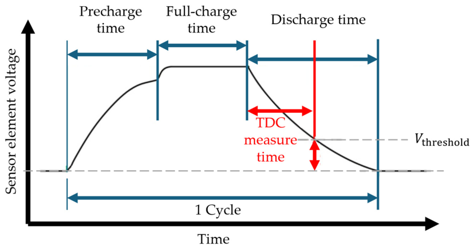
For capacitance measurement, a self-developed measurement unit is used. The capacitance measurement is based on a ScioSense (Eindhoven, The Netherlands) capacitance-to-digital converter. The underlying measurement principle of this integrated circuit is an RC circuit. The discharge time of this circuit is related to the sensor capacitance. Since the measurement is ratiometric, the same time-to-digital (TDC) unit is used for the measurement of the internal reference capacitance. Figure 7 shows the timing diagram including pre-charge time over an optional pre-charge resistor, full-charge time for the charging interval without a pre-charge resistor and discharge time, where the capacitance value is calculated from.
Figure 7.
Measurement of discharge time [15].
The PCap04 IC furthermore supports the compensation of parasitic internal and external capacitances, hence longer shielded cables between the sensor and measurement unit only marginally affect the measurement accuracy and precision. By averaging and performing dummy measurements for settling of the voltages using the digital signal processor (DSP) and the provided firmware, the measurement results do not necessarily need further post-processing. The measurement results are read out from the measurement IC via I2C by a microcontroller and transferred via serial interface to a computer.
The tests shown were conducted in a Comelec (La Chaux-de-Fonds, Switzerland) C-30H ALD and parylene coater. This system can coat parylene and atomic layers (e.g., ceramics). The parylene coating process is pressure-controlled. After vaporization and pyrolysis, the monomers are fed into a vacuum chamber for the CVD process. The excess parylene material is collected by a cryotrap located behind the chamber’s gas outlet, which leads to the vacuum pump. The CVD process that was applied for this paper has a vaporization temperature of 135 °C to 150 °C and a pyrolysis temperature of 670 °C. The coating duration depends on the target film thickness and can take up to 9 h for parylene C with a film thickness of over 20 µm.
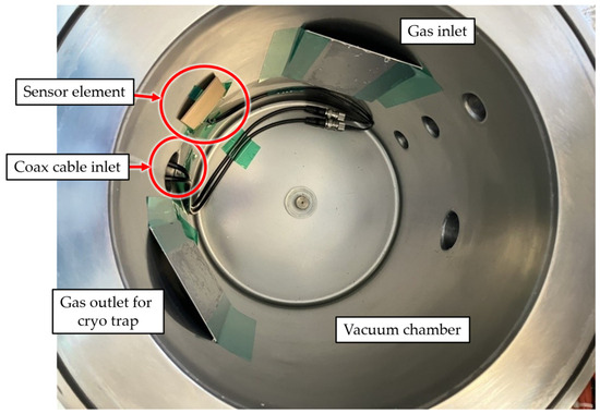
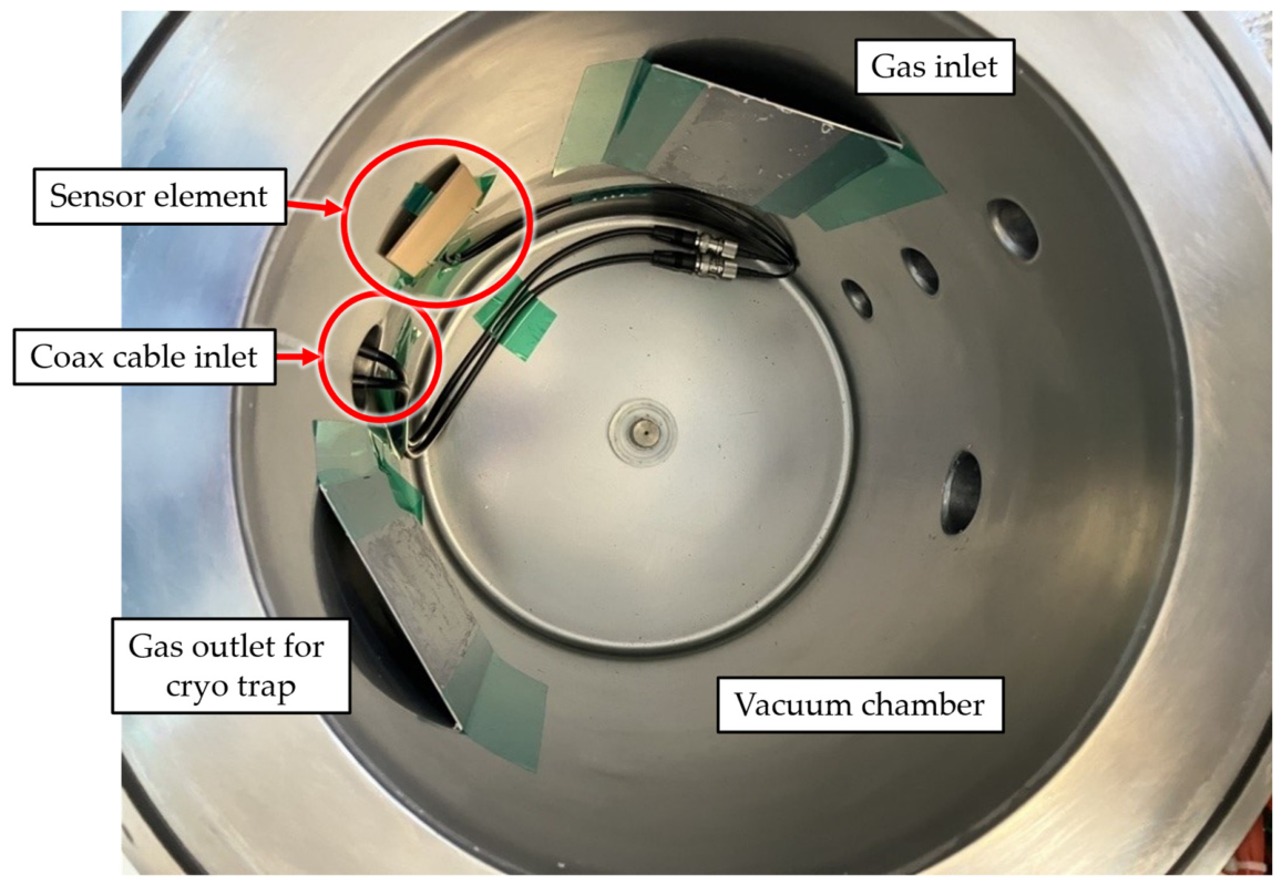
The capacitive sensor is mounted within the vacuum chamber and coated with parylene in the same process as other samples. In Figure 8, the inside of the vacuum chamber is depicted. The sensing area is oriented to the inside of the chamber, whilst the copper backplane is near the inner wall of the chamber. The sensing area should be left unobstructed to not affect the electric field or the coating process and, as a consequence, distort the measurement.
Figure 8.
Capacitance sensor inside the vacuum chamber.
3. Measurement Results
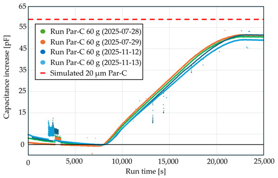
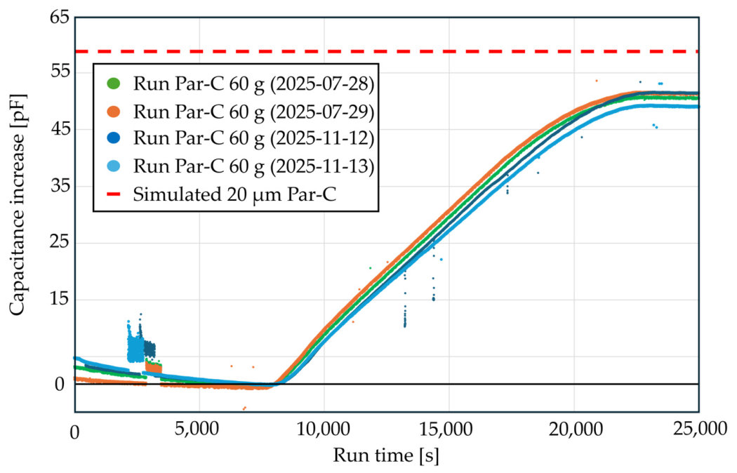
The sensor was tested with parylene C and F-VT4. Figure 9 shows the in situ measurement of the sensor capacitance over coating time. Four parylene C processes are shown, each with 60 g of raw material. The processes are named in the legend according to their start date. They are reproducible in terms of time sequence and measurement accuracy. After the processes, the in situ capacitance increase is always between 49 and 53 pF, which is below the simulated target increase of 58.6 pF for a 20 µm parylene thickness. The reproducibility of the results and the difference from the simulation indicate that a calibration measurement using cross-section comparison is recommended for each target parylene thickness and for each type of parylene.
Figure 9.
In situ capacitance increase in the sensor element during parylene C runs with 60 g of raw material.
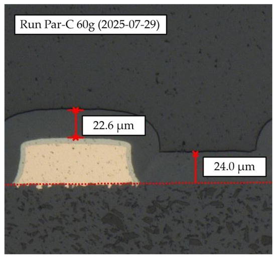
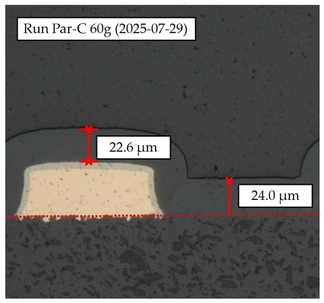
After the Par-C 60 g runs, the parylene layer of the four samples was checked in a micrograph: the measured thickness was between 20 and 25 µm for all sensor elements. Figure 10 shows an exemplary cross-section with the parylene height of 22.6 µm on top of the trace and 24.0 µm between 2 traces.
Figure 10.
Ground cross-section from a parylene-C 60 g run. (The red dotted line marks the interface between FR4 material and parylene/copper).
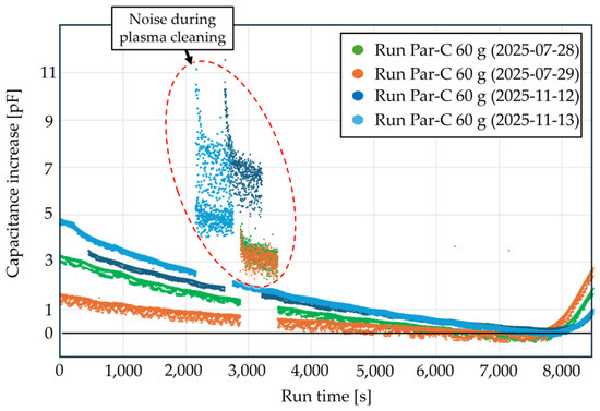
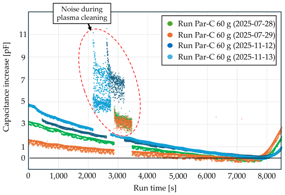
When zooming in on the starting phase of the CVD process, as shown in Figure 11, the measured capacitance of the sensor element decreases. At this stage, there is no coating material on the electrodes. This drift effect is due to vacuuming. It is reproducible and limited to a maximum of 8 pF for the presented sensor design. When analyzing the capacitance increase, the minimum capacitance right before injecting the parylene material into the CVD chamber is set to zero. Figure 11 also highlights the noisy area at the beginning of each parylene run. At this time interval, plasma cleaning takes place in the CVD chamber, which leads to the noisy offset.
Figure 11.
Zoom in on the starting phase of the coating process.
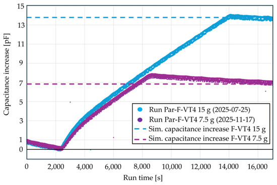
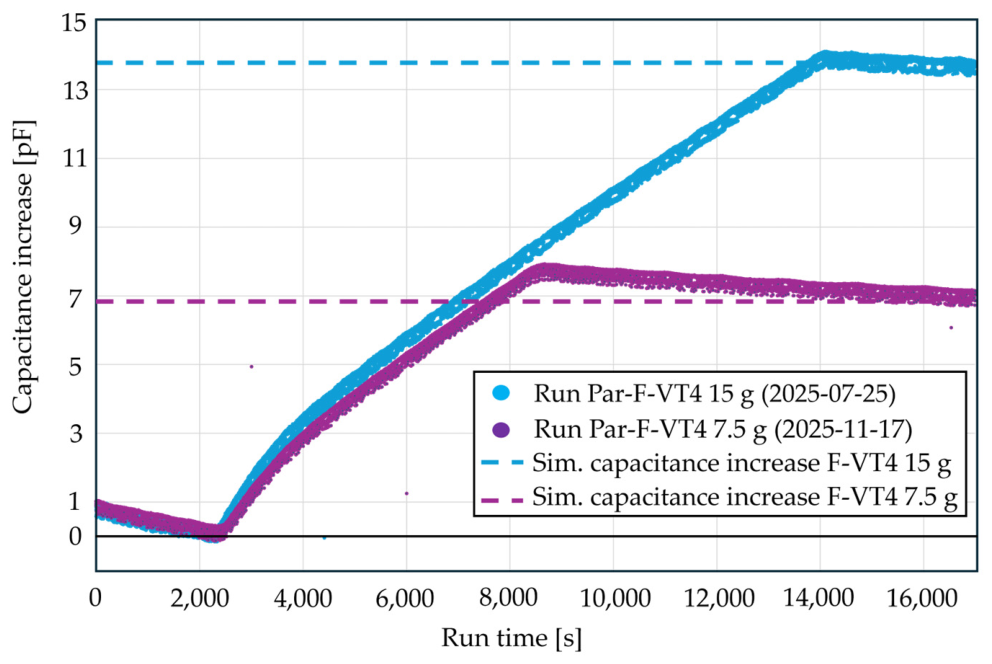
Figure 12 shows two F-VT4 parylene runs as another example. One with 7.5 g and one with 15 g of raw material. The F-VT4 run with 7.5 g of raw material results in a layer thickness of 2.5 µm. With 15 g of raw material, the thickness is approximately 5 µm. For both cases, the simulated expected capacitance increase is indicated. Here, the simulation and measurement match well.
Figure 12.
In situ capacitance increase in the sensor element during parylene F-VT4 runs with 7.5 g and 15 g raw material.
4. Conclusions and Next Steps
This work demonstrates that in situ layer thickness measurement for parylene CVD is feasible using capacitive sensing with interdigitated electrodes on a PCB. The method exploits the permittivity contrast between parylene and the surrounding vacuum environment.
Experimental validation with parylene C and F-VT4 confirmed the functionality of the approach. Four consecutive parylene C runs showed excellent reproducibility with capacitance increases between 49 and 53 pF, corresponding to verified layer thicknesses of 20 to 25 µm. The deviation of approximately 15 to 20% between measured and simulated values can be attributed to uncertainties in material properties and limitations of the two-dimensional simulation. For parylene F-VT4, the agreement between simulation and measurement was notably better.
The observed drift during the vacuum phase is systematic and compensable. The PCB-based design enables low-cost single-use sensor elements, eliminating cleaning between runs.
The primary goal for future work is the integration of the capacitance signal into a closed-loop control system, enabling dynamic adjustment of process parameters (e.g., vaporizing or pyrolysis temperature) to achieve target layer thicknesses with higher precision than current mass-based open-loop control.
Extension to additional parylene types would establish a comprehensive calibration database. For ultra-thin film applications, optimized sensor geometries with narrower electrode spacing could enhance sub-micron sensitivity.
Implementation of real-time thickness calculation would improve usability in production environments. Additionally, analysis of temporal capacitance profiles could enable process fingerprinting for quality assurance, where deviations from reference curves indicate process anomalies.
Author Contributions
Conceptualization, M.S., D.J. and J.W.; Methodology, M.S., D.J. and J.W.; Software, M.S. and D.J.; Validation, M.S., J.W. and H.R.; Formal analysis, M.S. and D.J.; Investigation, M.S. and J.W.; Resources, D.J. and J.W.; Data curation, M.S. and J.W.; Writing—original draft, M.S.; Writing—review & editing, M.S., D.J., H.R. and M.M.; Visualization, M.S., D.J. and J.W.; Supervision, H.R. and M.M.; Project administration, M.S. and H.R.; Funding acquisition, H.R. All authors have read and agreed to the published version of the manuscript.
Funding
This research was funded by the Federal ministry for economic affairs and climate action (grant number: 20M2107C).
Data Availability Statement
Additional data supporting the findings of this study are available from Manuel Seidenath (manuel.seidenath@iisb.fraunhofer.de) upon request.
Conflicts of Interest
The authors declare no conflict of interest.
References
- Hassler, C.; Boretius, T.; Stieglitz, T. Polymers for neural implants. J. Polym. Sci. B Polym. Phys. 2011, 49, 18–33. [Google Scholar] [CrossRef] [Scilit]
- Kim, H.; Najafi, K. Characterization of low-temperature wafer bonding using thin-film parylene. J. Microelectromech. Syst. 2005, 14, 1347–1355. [Google Scholar] [CrossRef] [Scilit]
- Gorham, W.F. A New, General Synthetic Method for the Preparation of Linear Poly-p-xylylenes. J. Polym. Sci. A 1 Polym. Chem. 1966, 4, 3027–3039. [Google Scholar] [CrossRef] [Scilit]
- Beach, W.F. A Model for the Vapor Deposition Polymerization of p-Xylylene. Macromolecules 1978, 11, 72–76. [Google Scholar] [CrossRef] [Scilit]
- Fortin, J.B.; Lu, T.-M. A Model for the Chemical Vapor Deposition of Poly(para-xylylene) (Parylene) Thin Films. Chem. Mater. 2002, 14, 1945–1949. [Google Scholar] [CrossRef] [Scilit]
- Liu, Y.; Kang, D.; Dai, W.; Li, H.; Wang, W.; Tai, Y.-C. Highly controllable and reliable ultra-thin Parylene deposition. Micro Nano Syst. Lett. 2018, 6, 5. [Google Scholar] [CrossRef] [Scilit]
- Jean, J.; Wang, A.; Bulović, V. In situ vapor-deposited parylene substrates for ultra-thin, lightweight organic solar cells. Org. Electron. 2016, 31, 120–126. [Google Scholar] [CrossRef] [Scilit]
- Lee, G.Y.; Ko, H.; Jung, H.W.; Ye, S.J.; Kim, M.H.; Pyun, J.C. On-line monitoring of parylene film deposition with quartz crystal microbalance (QCM). Procedia Eng. 2011, 25, 321–324. [Google Scholar] [CrossRef] [Scilit]
- Sutomo, W.; Wang, X.; Bullen, D.; Braden, S.K.; Liu, C. Development of an end-point detector for parylene deposition process. J. Microelectromech. Syst. 2003, 12, 64–69. [Google Scholar] [CrossRef]
- Taylor, R.C.; Welber, B. Laser-Monitored Deposition of Parylene Thin Films: Thin Solid Films; Elsevier Sequoia S.A.: Lausanne, Switzerland, 1975; pp. 221–226. [Google Scholar]
- Kim, Y.; Jung, B.; Lee, H.; Kim, H.; Lee, K.; Park, H. Capacitive humidity sensor design based on anodic aluminum oxide. Sens. Actuators B Chem. 2009, 141, 441–446. [Google Scholar] [CrossRef] [Scilit]
- Kurt, J.; Lesker Company. QCM Crystals for Thin Film Deposition Rate Monitoring. Available online: https://de.lesker.com/newweb/process_instruments/qcm-deposition-rate-monitoring-crystals.cfm (accessed on 12 May 2026).
- Comelec—Parylene Coating. Properties of Parylene. Available online: https://www.comelec.ch/wp-content/uploads/2020/11/Comelec_parylene_Properties.pdf (accessed on 28 September 2025).
- Chen, W.; Berwald, A.; Hauke, A.; Zimmermann, V.; Bayer, C.F.; Jank, M.P. Integration of a humidity sensor with power electronic applications. In Proceedings of the 2022 IEEE Sensors, Dallas, TX, USA, 30 October–2 November 2022; IEEE: Piscataway, NJ, USA, 2022; pp. 1–4. ISBN 978-1-6654-8464-0. [Google Scholar]
- Bhatti, W. PCAP04-Datasheet: Capacitance-to-Digital Converter. 2023. Available online: https://eu.mouser.com/new/sciosense/ams-pcap04-cdcs/?srsltid=AfmBOoqpZLoQpEtrOe4aSCo2W-faabu1bU3G1MPdrS41Mne7rFH5SufK (accessed on 13 March 2026).

Disclaimer/Publisher’s Note: The statements, opinions and data contained in all publications are solely those of the individual author(s) and contributor(s) and not of MDPI and/or the editor(s). MDPI and/or the editor(s) disclaim responsibility for any injury to people or property resulting from any ideas, methods, instructions or products referred to in the content. |
© 2026 by the authors. Licensee MDPI, Basel, Switzerland. This article is an open access article distributed under the terms and conditions of the Creative Commons Attribution (CC BY) license.