
Article

Amorphous GaOx Thin Film-Based Optoelectronic Artificial Synapses Towards Physical Reservoir Computing

1
Department of Applied Electronics, Graduate School of Advanced Engineering, Tokyo University of Science, Katsushika, Tokyo 125-8585, Japan
2
Nanomaterials and Microdevices Research Center, Osaka Institute of Technology, Osaka 535-8585, Japan
*
Author to whom correspondence should be addressed.
Electron. Mater. 2026, 7(2), 12; https://doi.org/10.3390/electronicmat7020012
Submission received: 11 April 2026 / Revised: 2 June 2026 / Accepted: 3 June 2026 / Published: 6 June 2026

Abstract

This study investigated the optoelectronic synaptic properties of amorphous gallium oxide (GaOx) thin films for low-power physical reservoir computing (PRC) applications. The fabricated devices were irradiated with time series UV-C light to characterize the paired pulse facilitation (PPF) index, a fundamental synaptic property governed by transient photocurrent dynamics. Furthermore, the short-term memory (STM) capacity and parity check (PC) nonlinearity were quantitatively evaluated as essential PRC performance metrics, alongside a practical demonstration using a handwritten digit recognition task. The experimental results revealed a high PPF index when the width and interval of the input light pulses were comparable to or shorter than the inherent photocurrent time constants of the device. Although the evaluated nonlinearity was lower than that of conventional optoelectronic artificial synapses based on other semiconductor materials, the GaOx device exhibited a comparable short-term memory capacity. Consequently, the reservoir layer achieved a high classification accuracy of approximately 90% in the handwritten digit recognition task. As these performance metrics were higher than those of the annealed sample, the device without annealing proved to be more suitable for PRC applications. These findings indicate that the amorphous GaOx thin film device holds significant potential to serve as a robust, UV-C-responsive edge artificial intelligence (AI) sensor in harsh environments, such as outer space.

1. Introduction

With the recent spread of IoT and cloud computing [1], the importance of edge processing has been recognized for enhancing information communication, and, in particular, edge artificial intelligence (AI) is attracting attention as a key technology for next-generation sensor devices [2]. As an important characteristic of edge AI, devices that can simultaneously perform sensing and AI information processing without relying on large-scale data transmission and reception are required. Physical reservoir computing (PRC) is a machine learning framework that uses physical devices to store and process information [3]. PRC is expected to be applied to widely deployed edge AI sensors, as it can perform real-time processing of temporal information due to its low power consumption.
Recently, PRC that can respond to time-varying light input has been attracting attention [4]. To realize PRC, one of the essential components is an optoelectronic synaptic device. The device has been fabricated using various materials and devices, including indium gallium zinc oxide (InGaZnO) [5], polymer–zinc oxide (ZnO) nanocomposites [6], gallium oxide (GaOx) [7], perovskite thin film [8], and dye-sensitized solar cells [9]. By adopting appropriate optoelectronic properties such as the bandgap and the highest occupied molecular orbital (HOMO)–lowest unoccupied molecular orbital (LUMO) gap, light with a specific wavelength can be processed. In space application, on space objects such as spacecraft and lunar structures, external photoelectric effects caused by UV-C and electron collisions generate strong electric fields, leading to localized discharges that may damage or destroy the electrical components [10]. To avoid failures, a sensor that can predict and classify temporal UV-C light is required, with low power consumption. Edge AI sensors based on PRC with optoelectronic artificial synapses that respond to UV-C satisfy the above requirements.
Among various candidate materials, conventional oxide semiconductors have been widely studied for synapses featuring analog plasticity [11,12,13]. However, they often lack intrinsic solar-blind characteristics. In contrast, GaOx is a wide-bandgap semiconductor that responds to UV-C light and is a promising candidate for optoelectronic artificial synapse targeting for the applications mentioned above [14,15]. In particular, amorphous GaOx exhibits high UV-C responsiveness and lower power consumption compared to other crystalline phases, while offering the advantage of low-cost fabrication without annealing [16,17]. While research on its application to neuromorphic computing is progressing [7,18,19], the performance metrics for its application to PRC have not been fully investigated. For instance, crucial metrics such as paired pulse facilitation (PPF), short-term memory (STM) tasks, parity check (PC) tasks, and handwriting recognition tasks have not been sufficiently explored for GaOx.
In this study, we fabricated amorphous GaOx thin film devices and systematically characterized their performance metrics to assess their operation as PRC reservoir layers. The findings obtained in this study are expected to significantly contribute to the development of amorphous GaOx-based optoelectronic synaptic devices for PRC applications.

2. Materials and Methods

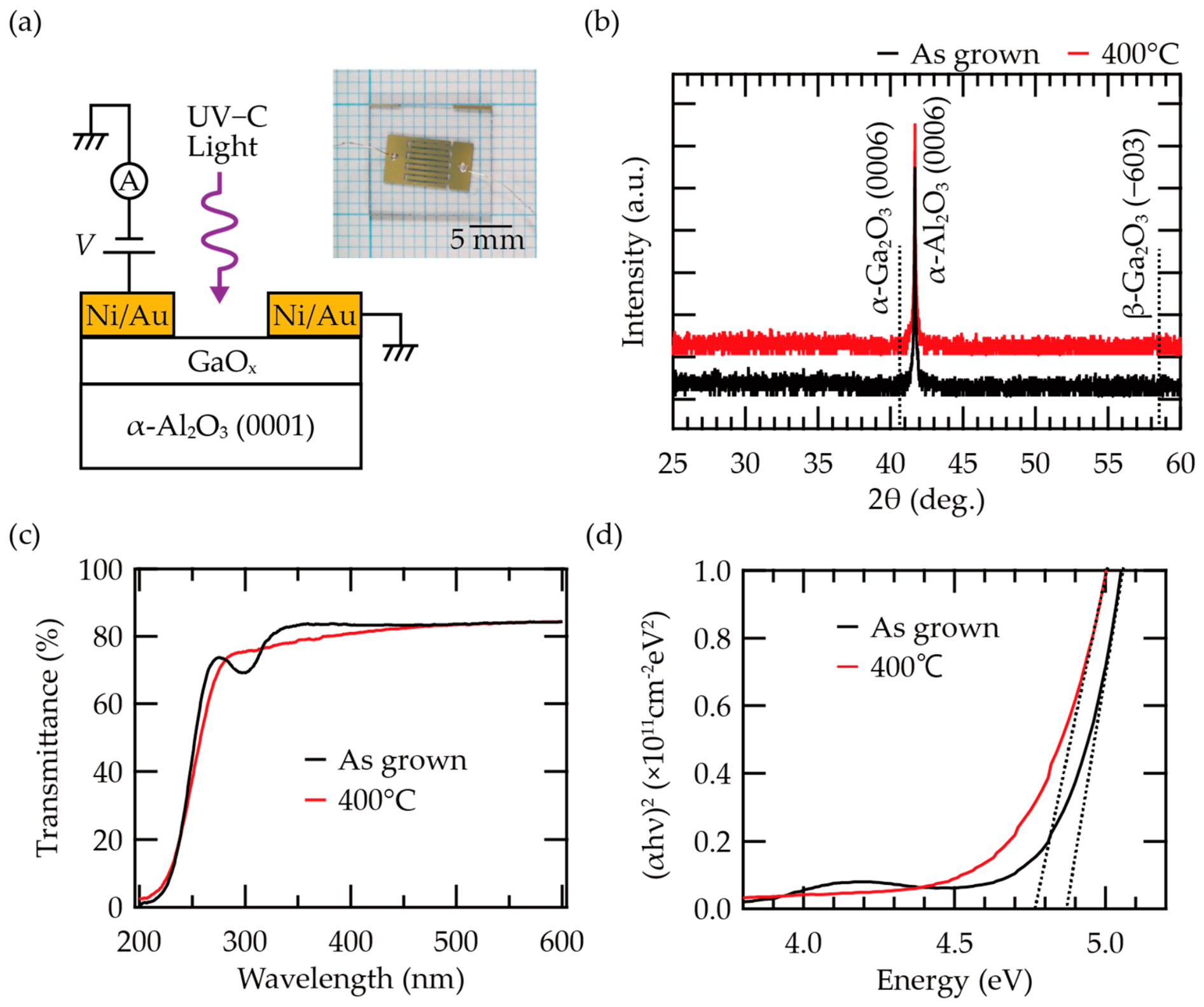
Figure 1a shows a schematic illustration of the GaOx-based synaptic device. First, a squared α-Al2O3 (0001) wafer (Furuuchi Chemical, Tokyo, Japan) with a lateral dimension of 10 mm was organically cleaned with toluene, acetone, and isopropyl alcohol, followed by a mixture of sulfuric acid and phosphoric acid. Subsequently, the substrate was introduced into a fine-channel mist chemical vapor deposition (CVD) system for GaOx thin film deposition. The source precursor solution was prepared by dissolving gallium (III) acetylacetonate (14405-43-7, Sigma-Aldrich Co. LLC, St. Louis, MO, USA) in ultrapure water with a precursor concentration of 0.05 M. The precursor mist, which was generated by an ultrasonic transducer from the solution, was transferred into the fine-channel furnace with flowing air as the carrier gas and the dilution gas at rates of 1 LPM and 1 LPM, respectively. The furnace temperature was maintained at 260 °C, and the deposition time was 60 min. The resultant thin film had a thickness of approximately 170 nm. After deposition, post-annealing at 400 °C was performed using a tubular electric furnace (ARF-50KC, Asahi-rika Co., Ltd., Chiba, Japan). The annealing time and the air flow rate were 60 min and 1 LPM, respectively. The detailed fabrication process has been already described elsewhere [20].
The crystallinity and optical transmittance of the obtained GaOx thin film were characterized using X-ray diffraction (XRD: SmartLab, Rigaku Corp., Tokyo, Japan) and a UV-vis-IR spectrometer (UV-3600Plus, SHIMADZU CORPORATION, Kyoto, Japan), respectively. Then, to observe the temporal variation in the photocurrent, an interdigitated Ni/Au multilayer electrode, with thicknesses of 50 and 100 nm, respectively, was formed on the surface of the GaOx thin film. The channel width and the channel length were approximately 35.6 mm and 0.2 mm, respectively, and the number of combs was 9. The time constant of the photocurrent was measured. A power supply (GPD-2303S, GWINSTEK, Kanagawa, Japan) was used to apply 10 V between the electrodes while irradiating the sample with a square wave of deep-UV light (UXM-500SX, Ushio Inc., Tokyo, Japan). Then, we measured a synaptic property such as PPF. Pulsed UV light, which was formed using the deep-UV light with a mechanical shutter (LS6, Vincent Associates, Rochester, NY, USA), was irradiated to the device. The total illuminated area was approximately 7.1 mm2. The photocurrent was measured using a DAQ device (USB-6366, National Instruments, Austin, TX, USA) via a current–voltage amplifier (T-IVA001MAC, Turtle Industries, Ibaraki, Japan). Furthermore, to characterize the performance as a reservoir layer of PRC, the STM task and PC task were adopted [21]. The STM task measures the ability to reproduce past inputs and is used as a benchmark task to characterize short-term memory. On the other hand, the PC task characterizes nonlinearity by assessing tasks such as exclusive OR (XOR) and the ability to reproduce past inputs, serving as a benchmark task for nonlinearity assessment. The training phase utilized transient responses to a sequence of 1000 random binary UV pulses to determine the readout weights. In this sequence, the binary states of ‘1’ and ‘0’ correspond to the presence and absence of UV irradiation, respectively. Each pulse had a width of 0.5 s, and the number of virtual nodes was set to 5. To evaluate the correlation, these trained weights were multiplied by the transient responses from a separate sequence of 1000 pulses, and the resulting output was compared with a time-delayed version of the input sequence. The details are described in a previous study [6]. In addition, we demonstrated a hand-written digit recognition task using MNIST. The detailed experimental conditions related to the above tasks are described elsewhere [21,22,23,24,25].

3. Results and Discussion

3.1. Structural and Optical Properties of GaOx Thin Film

Figure 1b shows the XRD patterns of the films without and with post-annealing. The peak observed at 41.68° is attributed to α-Al2O3 (0006) (PDF 04-007-5143). Regardless of annealing, no peaks corresponding to Ga2O3 were observed. Figure 1c shows optical transmittance as a function of the wavelength. Both samples exhibited transparency in the visible region, with reduced transmittance in the UV region below 300 nm. Figure 1d shows the Tauc plots of the films. The optical bandgap was determined from the intersection of the extrapolated linear region of (αhν)2 and the horizontal axis. The optical bandgaps of the samples without and with post-annealing were 4.86 and 4.75 eV, respectively. These values were smaller than that of GaOx thin films, which was reported to be 5.17 eV [26]. The narrowing bandgap might be due to the formation of intra-gap states at shallow positions in the gap, which reduced the apparent optical bandgap [27].

3.2. Optoelectronic Synaptic Properties of GaOx Thin Film

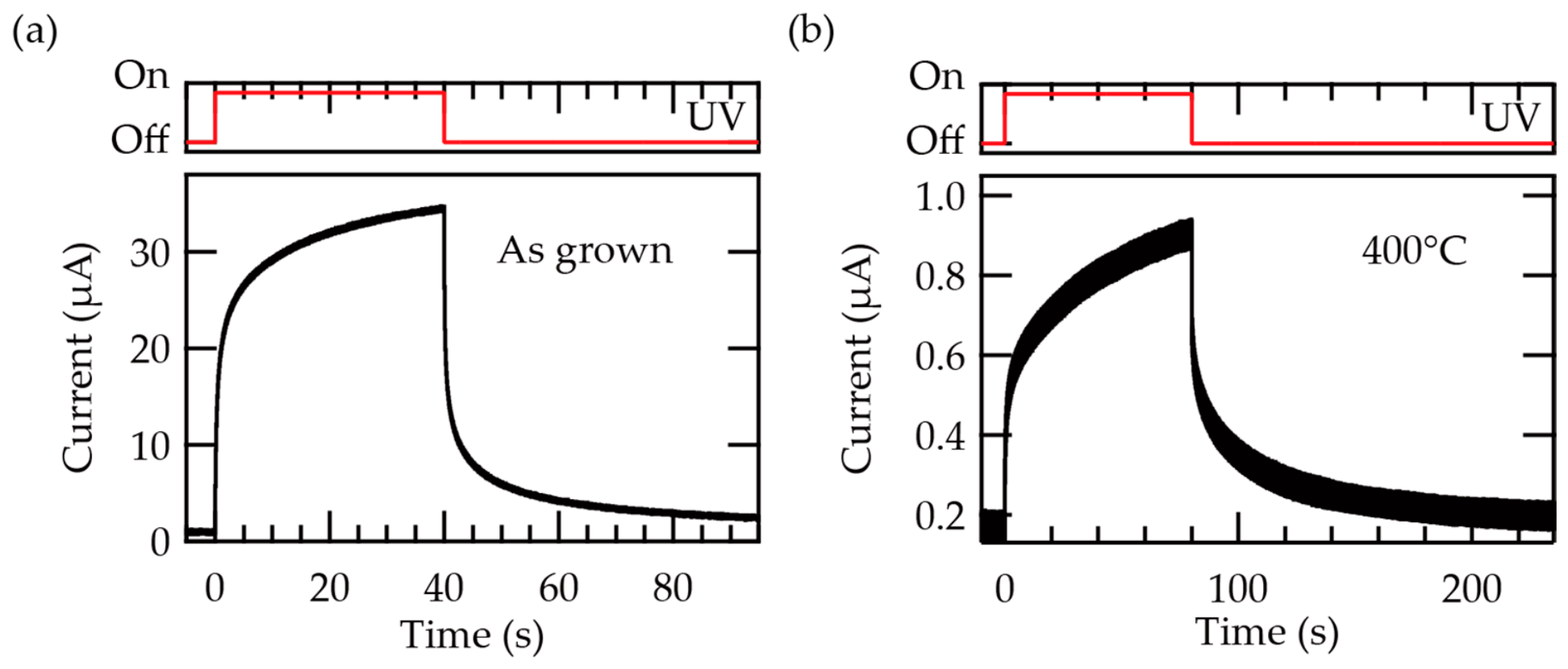
Figure 2a,b show transient responses of the samples without and with post-annealing during UV pulse irradiation. The photocurrent gradually increased during UV-C irradiation. The current values just before stopping UV light irradiation, after continuously irradiating devices without and with annealing for a certain period, were 34.48 µA and 0.91 µA, respectively. When UV irradiation was stopped, the photocurrent gradually decreased for both samples. This result is likely due to persistent photoconductivity (PPC) [17,28,29].
For further analysis, the transient response curves of the photocurrent were fitted by the following equations:
I r t =   I 0 +   n = 1 N A n 1 e x p t t 0 τ r n
I d t = I 0 + n = 1 N B n e x p t t 0 τ d n
where Ir(t), Id(t), and I0 are the transient photocurrent with light irradiation, the transient photocurrent without light irradiation, and the steady-state photocurrent, respectively. An and Bn are the constants, t is the time, t0 is the time when the change in photocurrent begins, and τrn and τdn are the time constants. Fitting was performed for N = 3, which adequately described each transient response. τr1, τr2, and τr3 for the as-grown sample were 0.192, 1.55, and 16.69 s, respectively, and τd1, τd2, and τd3 were 0.160, 1.62, and 14.39 s, respectively. τr1, τr2, and τr3 for the 400 °C annealed sample were 0.07, 1.91, and 43.61 s, respectively, and τd1, τd2, and τd3 were 0.24, 8.78, and 54.15 s, respectively. Some previous reports defined the time required for a 10% to 90% increase and a 90% to 10% decrease in photocurrent as τr and τd, respectively [16,30]. Other reports used the equations as mentioned above, with N of 1 [31,32,33] and N of 2 [34,35,36]. While the shorter time constants in our experiment were similar to those reported previously, the longer time constants observed were notably higher.
It is known that the photocurrent is composed of two components [37]. The transport of photoexcited carriers can mainly be classified into two types: drift current due to the strong electric field between the electrodes, and slow transport mediated by trap–detrapping at gap states such as Vo defects. The former is considered the origin of the short time constant in the transient response of the photocurrent, while the latter accounts for the long time constant. The reason for fitting with three time constants is likely due to the presence of two slow transport paths. Since the precise origins of these time constants remain speculative, further investigation into the carrier transport phenomena will be conducted in the future.
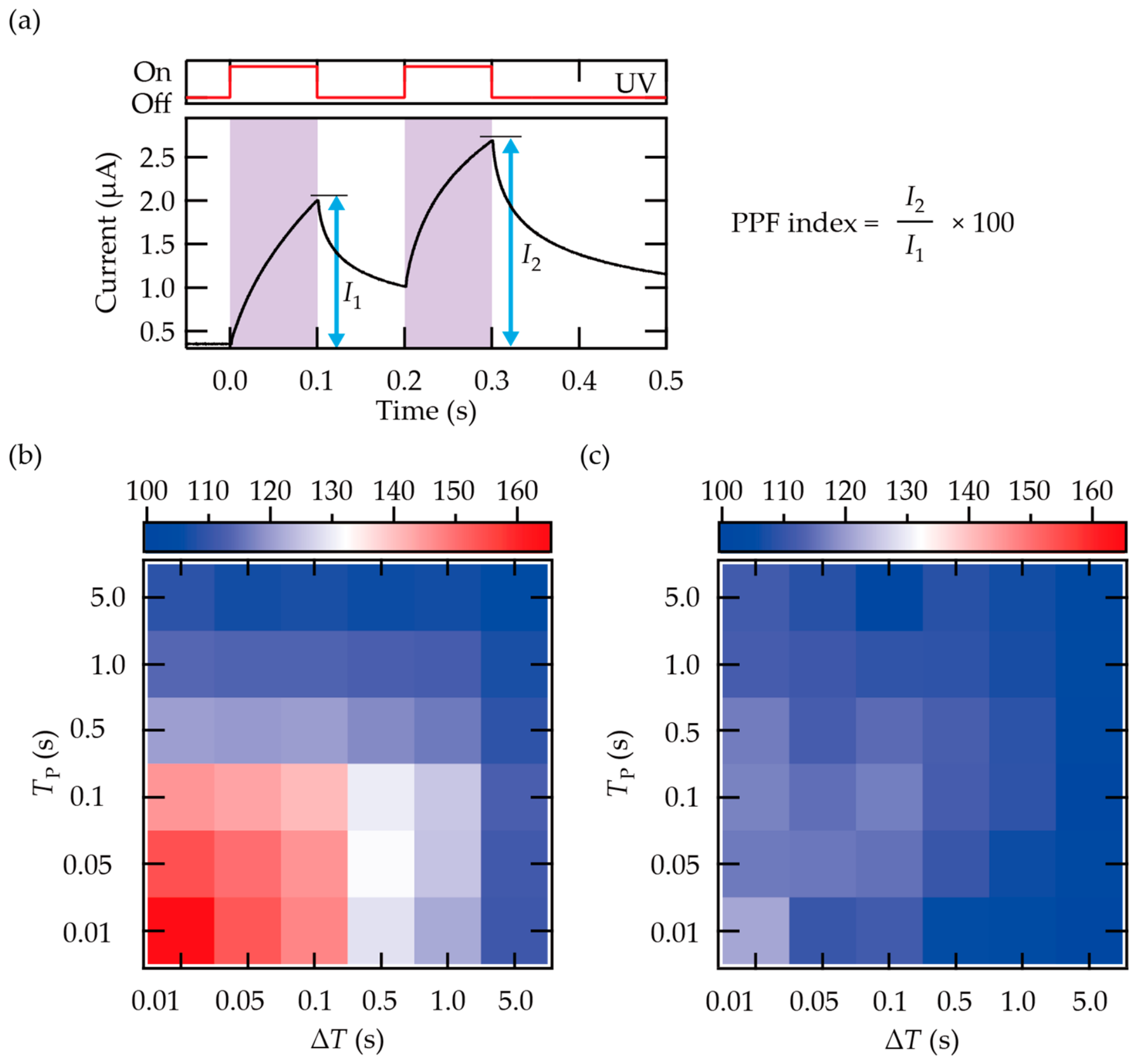
Based on the slow transient photocurrent dynamics originating from the gap states, we further investigated the potential of the GaOx films for artificial optoelectronic synapse applications. The PPF index is defined as the ratio of the intensities of two peaks when two pulses are applied to the device [6], as shown in Figure 3a. Figure 3b,c show the PPF indices of samples without and with annealing, respectively, for different pulse durations Tp and ΔT. At Tp = 0.01 s and ΔT = 0.01 s, the PPF values for the samples without and with annealing were 164.5% and 119.9%, respectively. As shown in Figure 3b,c, the without-annealing sample had a PPF index of over 130% when Tp was less than 0.1 s and ΔT was less than 0.5 s. However, the PPF index did not exceed 130% for the sample with annealing. When Tp < τr1 and ΔT< τd1, the PPF tends to be large because the photocurrent increases or decreases significantly. Previous reports suggested that the transient properties of artificial synapses can be reproduced using a series circuit of a resistor (R) and a capacitor (C) [38]. However, the present results cannot be reproduced by a simple RC circuit. The reason why might be that the time constants of photocurrents in the first and second pulses were different. It is considered that the time constant of the photocurrent during the second light irradiation differed from that of the first light irradiation because the gap states were partially occupied by photoexcited carriers from the first irradiation. In the future, precise defect control will be necessary to match the operating time range of the device to the time scale of the application because the gap states are crucial to control the time constants.

3.3. Reservoir Computing Tasks and Handwriting Recognition Demonstration

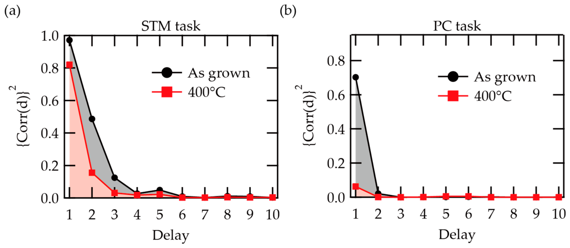
The results of the STM and PC tasks are shown in Figure 4. Figure 4a shows that the determination coefficients with a delay of 1 for the without- and with-annealing samples were estimated to be 0.97 and 0.82, respectively. The correlation coefficients at delay 3 for the samples without and with annealing were 0.12 and 0.03, respectively. The memory capacity (CSTM) is the sum of the determination coefficients for all delays in the STM task [21]. The CSTM of the without- and with-annealing samples was 1.62 and 1.05, respectively. The CSTM of GaOx has not been investigated yet. Compared with the CSTM of the ZnO-CNF-based optoelectronic artificial synapse, which was 1.8 [6], the CSTM of GaOx was slightly smaller than this value. Figure 4b shows that the determination coefficients for samples without and with annealing in the PC task were 0.70 and 0.063, respectively. When delay was 2, the determination coefficients of the former and the latter samples were 0.02 and 0.001, respectively. The parity check capacity (CPC) is the sum of the determination coefficients for all delays in the PC task. The CPC for the samples without and with annealing were 0.731 and 0.066, respectively. Since the PC task requires recall of past inputs as well as the STM task, it is likely that the PC tends to be small when the CSTM is small. CSTM and CPC were found to decrease after annealing. In other words, annealing the sample reduces the ability to store information.
We hypothesize that the annealing process improves the crystallinity of the films and reduces the number of trap sites, leading to a decrease in the recombination rate. This leads to shorter time constants and quick saturation or relaxation, resulting in lower CSTM and CPC. Future structural analyses will be necessary to experimentally verify this hypothesis. Furthermore, from the perspective of computing performance, it should be noted that the required CPC value depends on the complexity of the target task. A low CPC indicates limited nonlinearity, which restricts the computational capacity of the reservoir and makes it difficult to process complex calculations. Therefore, when applying the reservoir to tasks that inherently demand high nonlinearity, it is necessary to utilize devices with a higher CPC. To improve the nonlinearity, possible methods include optimizing the deposition conditions, controlling the defect states, and inducing ionic conductivity [39,40].
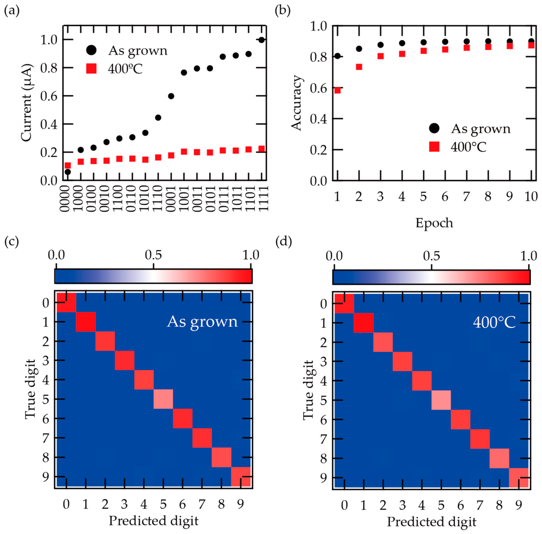
For the handwriting recognition task, samples without and with annealing were irradiated with 16 patterns of 4-bit pulses. Figure 5a shows the current values at 2 ms after the end of each irradiation. Different current values were obtained for each pulse for the without-annealing sample, while no significant change was observed for each pulse for the with-annealing sample. Figure 5b shows the accuracy of the number recognition for each epoch for the samples without and with annealing. For the without-annealing sample, the accuracy was 80% and 90% for epochs of 1 and 10, respectively. For the with-annealing sample, the accuracy was 58% and 87% at epochs of 1 and 10, respectively. The annealing process decreased the accuracy at any number of epochs. The accuracies of the β-Ga2O3-based optical synaptic device and the ZnO-CNF-based optoelectronic artificial synapse were 78% and 88%, respectively [6,36]. The accuracy of the sample without annealing, at an epoch of 10, was higher than these values. Figure 5c,d show the confusion matrix for the samples without and with annealing, respectively, at epochs of 10. Both samples were shown to exhibit a high probability of recognizing and classifying numbers.
Although this initial proof-of-concept evaluation is currently limited to a single representative device, the findings obtained in this study demonstrate the performance of the amorphous GaOx reservoir layer. These insights are expected to significantly contribute to the further development of amorphous GaOx-based optoelectronic synaptic devices for PRC applications.

4. Conclusions

In conclusion, we investigated the optoelectronic synaptic properties of amorphous GaOx thin films. It was revealed that the transient response curve of the photocurrent during UV light irradiation consists of a linear combination of three exponential functions with different time constants: sub-seconds, seconds, and tens of seconds. By annealing the samples, most of the time constants were extended. The characterization of the PPF index for various Tp and ΔT for two consecutive light pulses revealed that, when Tp was equal to or shorter than the fast time constant, it exhibited higher values compared to other pulse conditions. To characterize the performance as a PRC, STM and PC tasks were conducted, and our device showed a CSTM of 1.62 and a CPC of 0.731. Although these values are lower compared to ZnO-based synaptic devices [6], there is room for improvement through the control of the shape, crystallinity, and oxygen vacancies in GaOx thin films. Furthermore, using our device as the reservoir layer in PRC, we conducted a handwritten digit recognition task and found that it achieved a high accuracy of approximately 90%. Therefore, the performance comparison revealed that the device without annealing is more suitable for PRC applications than the device with annealing, demonstrating that the amorphous GaOx thin films have potential for utilization as PRC devices.
In the future, we aim to develop synaptic devices that operate within the desired time range and explore their application in PRC. For example, to realize an AI optoelectronic sensor that uses time series light related to biological signals as input data, it is necessary to develop a device with the highest CSTM in the sub-second to second range. This will require controlling the material properties such as the density of gap states and interface states. By envisioning various applications, we believe that it will be possible to achieve more versatile or specialized devices for PRC.

Author Contributions

Conceptualization, T.I.; methodology, H.K., T.I. and K.T.; software, K.T. and H.K.; validation, K.T., H.K. and T.K.; formal analysis, K.T. and H.K.; investigation, K.T.; resources, K.T., M.M., I.Y. and M.K.; data curation, K.T.; writing—original draft preparation, K.T. and T.I.; writing—review and editing, K.T. and T.I.; visualization, K.T.; supervision, T.I.; project administration, T.I.; funding acquisition, H.K. and T.I. All authors have read and agreed to the published version of the manuscript.

Funding

This work was partially supported by the JST and the establishment of university fellowships for the creation of science and technology innovation (Grant Number JPMJFS2144). Additional support was provided by the JST SPRING (Grant Number JPMJSP2151), JSPS KAKENHI (Grant number 26K01350), the Murata Science Foundation, and the Tokyo University of Science Grant for Raising Next-Generation Researchers.

Data Availability Statement

The raw data supporting the conclusions of this article will be made available by the authors on request.

Conflicts of Interest

The authors declare no conflicts of interest. The funders had no role in the design of the study; in the collection, analyses, or interpretation of data; in the writing of the manuscript; or in the decision to publish the results.

References

  1. Armbrust, M.; Fox, A.; Griffith, R.; Joseph, A.D.; Katz, R.; Konwinski, A.; Lee, G.; Patterson, D.; Rabkin, A.; Stoica, I.; et al. A View of Cloud Computing. Commun. ACM 2010, 53, 50–58. [Google Scholar] [CrossRef] [Scilit]
  2. Shi, W.S.; Cao, J.; Zhang, Q.; Li, Y.H.Z.; Xu, L.Y. Edge Computing: Vision and Challenges. IEEE Internet Things J. 2016, 3, 637–646. [Google Scholar] [CrossRef] [Scilit]
  3. Tanaka, G.; Yamane, T.; Héroux, J.B.; Nakane, R.; Kanazawa, N.; Takeda, S.; Numata, H.; Nakano, D.; Hirose, A. Recent advances in physical reservoir computing: A review. Neural Netw. 2019, 115, 100–123. [Google Scholar] [CrossRef] [Scilit]
  4. Chen, Z.L.; Xiao, Y.; Huang, W.Y.; Jiang, Y.P.; Liu, Q.X.; Tang, X.G. In-sensor reservoir computing based on optoelectronic synaptic devices. Appl. Phys. Lett. 2023, 123, 100501. [Google Scholar] [CrossRef] [Scilit]
  5. Yang, Y.; Cui, H.Y.; Ke, S.; Pei, M.J.; Shi, K.L.; Wan, C.J.; Wan, Q. Reservoir computing based on electric-double-layer coupled InGaZnO artificial synapse. Appl. Phys. Lett. 2023, 122, 043508. [Google Scholar] [CrossRef] [Scilit]
  6. Komatsu, H.; Hosoda, N.; Kounoue, T.; Tokiwa, K.; Ikuno, T. Disposable and Flexible Paper-Based Optoelectronic Synaptic Devices for Physical Reservoir Computing. Adv. Electron. Mater. 2024, 10, 2300749. [Google Scholar] [CrossRef] [Scilit]
  7. Zhang, Z.F.; Zhao, X.L.; Zhang, X.M.; Hou, X.H.; Ma, X.L.; Tang, S.Z.; Zhang, Y.; Xu, G.W.; Liu, Q.; Long, S.B. In-sensor reservoir computing system for latent fingerprint recognition with deep ultraviolet photo-synapses and memristor array. Nat. Commun. 2022, 13, 6590. [Google Scholar] [CrossRef] [Scilit]
  8. Cao, Y.; Zhao, C.; Yin, L.; Shi, L.; Zhou, J.; Zhang, Z.Y.; Wu, R.; Yang, Q.Y.; Yuan, M.; Gu, M. Perovskite-based optoelectronic artificial synaptic thin-film transistor. Solid State Electron. 2023, 208, 108713. [Google Scholar] [CrossRef] [Scilit]
  9. Yamada, R.; Nakagawa, M.; Hirooka, S.; Tada, H. Physical reservoir computing with visible-light signals using dye-sensitized solar cells. Appl. Phys. Express 2024, 17, 097001, Correction in Appl. Phys. Express 2024, 17, 119301. https://doi.org/10.35848/1882-0786/ad8c20. [Google Scholar] [CrossRef] [Scilit]
  10. Garrett, H.B.; Whittlesey, A.C. Spacecraft charging, an update. IEEE Trans. Plasma Sci. 2000, 28, 2017–2028. [Google Scholar] [CrossRef]
  11. Wang, W.X.; Kim, N.Y.; Lee, D.M.; Yin, F.F.; Niu, H.S.; Ganbold, E.; Park, J.W.; Shin, Y.K.; Li, Y.; Kim, E.S. Operant conditioning reflex implementation in a transparent Ta2O5-3x/ Ta2O5_x homo-structured optoelectronic memristor for neuromorphic computing application. Nano Energy 2024, 119, 109102. [Google Scholar] [CrossRef] [Scilit]
  12. Cao, X.Q.; Zheng, Q.Q.; Wang, L.B.; Lin, Z.F.; Meng, J.; Xu, S.L.; Huang, Y.Y.; Deng, W. Transparent ZnO/InO Heterojunction Artificial Synapse for Neuromorphic Computing and Logical Operations. Acs Appl. Electron. Mater. 2026, 8, 1902–1917. [Google Scholar] [CrossRef] [Scilit]
  13. Martins, R.A.; Silva, C.; Deuermeier, J.; Milano, G.; Rosero-Realpe, M.; Parreira, C.; Fortunato, E.; Martins, R.; Kiazadeh, A.; Carlos, E. Printed Zinc Tin Oxide Memristors for Reservoir Computing. Adv. Intell. Syst. 2026, 8, 2500450. [Google Scholar] [CrossRef] [Scilit]
  14. Zhu, R.; Hang, H.L.; Hu, S.G.; Wang, Y.; Mei, Z.X. Amorphous-Ga2O3 Optoelectronic Synapses with Ultra-low Energy Consumption. Adv. Electron. Mater. 2022, 8, 2100741. [Google Scholar] [CrossRef] [Scilit]
  15. Al-Hardan, N.H.; Hamid, M.A.A.; Jalar, A.; Firdaus-Raih, M. Unleashing the potential of gallium oxide: A paradigm shift in optoelectronic applications for image sensing and neuromorphic computing applications. Mater. Today Phys. 2023, 38, 101279. [Google Scholar] [CrossRef] [Scilit]
  16. Qian, L.X.; Wu, Z.H.; Zhang, Y.Y.; Lai, P.T.; Liu, X.Z.; Li, Y.R. Ultrahigh-Responsivity, Rapid-Recovery, Solar-Blind Photodetector Based on Highly Nonstoichiometric Amorphous Gallium Oxide. ACS Photonics 2017, 4, 2203–2211. [Google Scholar] [CrossRef] [Scilit]
  17. Wang, J.; Xiong, Y.Q.; Ye, L.J.; Li, W.J.; Qin, G.P.; Ruan, H.B.; Zhang, H.; Fang, L.; Kong, C.Y.; Li, H.L. Balanced performance for β-Ga2O3 solar blind photodetectors: The role of oxygen vacancies. Opt. Mater. 2021, 112, 110808. [Google Scholar] [CrossRef] [Scilit]
  18. Gao, X.X.; Zhang, H.; Feng, Y.L.; Li, J.; Chen, Y.F.; Zhang, M.; Lin, Z.H.; Zhang, J.C.; Hao, Y.; Chang, J.J. Recent Breakthroughs in Gallium Oxide-Based Optoelectronic Devices for Neuromorphic Computing. Adv. Funct. Mater. 2026, e75385. [Google Scholar] [CrossRef] [Scilit]
  19. Pearton, S.J.; Yang, J.C.; Cary, P.H.; Ren, F.; Kim, J.; Tadjer, M.J.; Mastro, M.A. A review of Ga2O3 materials, processing, and devices. Appl. Phys. Rev. 2018, 5, 011301. [Google Scholar] [CrossRef] [Scilit]
  20. Miyazaki, M.; Yamasaki, I.; Tanaka, Y.; Koyama, M.; Fujii, A.; Maemoto, T. UV Detection Properties of Mist CVD Grown Amorphous Ga2O3 Thin Films. In Proceedings of the IEICE Technical Committee on Electron Devices, Kochi, Japan, 23 August 2024. [Google Scholar]
  21. Tsunegi, S.; Taniguchi, T.; Miwa, S.; Nakajima, K.; Yakushiji, K.; Fukushima, A.; Yuasa, S.; Kubota, H. Evaluation of memory capacity of spin torque oscillator for recurrent neural networks. Jpn. J. Appl. Phys. 2018, 57, 120307. [Google Scholar] [CrossRef] [Scilit]
  22. Furuta, T.; Fujii, K.; Nakajima, K.; Tsunegi, S.; Kubota, H.; Suzuki, Y.; Miwa, S. Macromagnetic Simulation for Reservoir Computing Utilizing Spin Dynamics in Magnetic Tunnel Junctions. Phys. Rev. Appl. 2018, 10, 034063. [Google Scholar] [CrossRef] [Scilit]
  23. Watt, S.; Kostylev, M. Reservoir Computing Using a Spin-Wave Delay-Line Active-Ring Resonator Based on Yttrium-Iron-Garnet Film. Phys. Rev. Appl. 2020, 13, 034057. [Google Scholar] [CrossRef] [Scilit]
  24. Koh, S.G.; Shima, H.; Naitoh, Y.; Akinaga, H.; Kinoshita, K. Reservoir computing with dielectric relaxation at an electrode-ionic liquid interface. Sci. Rep. 2022, 12, 6958. [Google Scholar] [CrossRef] [Scilit]
  25. Midya, R.; Wang, Z.R.; Asapu, S.; Zhang, X.M.; Rao, M.Y.; Song, W.H.; Zhuo, Y.; Upadhyay, N.; Xia, Q.F.; Yang, J.J. Reservoir Computing Using Diffusive Memristors. Adv. Intell. Syst. 2019, 1, 1900084. [Google Scholar] [CrossRef] [Scilit]
  26. Kumar, S.S.; Rubio, E.J.; Noor-A-Alam, M.; Martinez, G.; Manandhar, S.; Shutthanandan, V.; Thevuthasan, S.; Ramana, C.V. Structure, Morphology, and Optical Properties of Amorphous and Nanocrystalline Gallium Oxide Thin Films. J. Phys. Chem. C 2013, 117, 4194–4200. [Google Scholar] [CrossRef] [Scilit]
  27. Guan, S.J.; Cheng, Y.L.; Hao, L.; Yoshida, H.; Tarashima, C.; Zhan, T.Z.; Itoi, T.; Qiu, T.B.; Lu, Y. Oxygen vacancies induced band gap narrowing for efficient visible-light response in carbon-doped TiO2. Sci. Rep. 2023, 13, 14105. [Google Scholar] [CrossRef] [Scilit]
  28. Studenikin, S.A.; Golego, N.; Cocivera, M. Optical and electrical properties of undoped ZnO films grown by spray pyrolysis of zinc nitrate solution. J. Appl. Phys. 1998, 83, 2104–2111. [Google Scholar] [CrossRef] [Scilit]
  29. Reemts, J.; Kittel, A. Persistent photoconductivity in highly porous ZnO films. J. Appl. Phys. 2007, 101, 013709. [Google Scholar] [CrossRef] [Scilit]
  30. Zhang, Y.F.; Chen, X.H.; Xu, Y.; Ren, F.F.; Gu, S.L.; Zhang, R.; Zheng, Y.D.; Ye, J.D. Transition of photoconductive and photovoltaic operation modes in amorphous Ga2O3-based solar-blind detectors tuned by oxygen vacancies. Chin. Phys. B 2019, 28, 028501. [Google Scholar] [CrossRef] [Scilit]
  31. Han, Z.Y.; Liang, H.L.; Huo, W.X.; Zhu, X.S.; Du, X.L.; Mei, Z.X. Boosted UV Photodetection Performance in Chemically Etched Amorphous Ga2O3 Thin-Film Transistors. Adv. Opt. Mater. 2020, 8, 1901833. [Google Scholar] [CrossRef] [Scilit]
  32. Zhou, C.Q.; Liu, K.W.; Chen, X.; Feng, J.H.; Yang, J.L.; Zhang, Z.Z.; Liu, L.; Xia, Y.; Shen, D.Z. Performance improvement of amorphous Ga2O3 ultraviolet photodetector by annealing under oxygen atmosphere. J. Alloy. Compd. 2020, 840, 155585. [Google Scholar] [CrossRef] [Scilit]
  33. Polyakov, A.Y.; Almaev, A.V.; Nikolaev, V.I.; Pechnikov, A.I.; Shchemerov, V.I.; Vasilev, A.A.; Yakimov, E.B.; Kochkova, A.I.; Kopyev, V.V.; Kushnarev, B.O.; et al. Mechanism for Long Photocurrent Time Constants in α-Ga2O3 UV Photodetectors. ECS J. Solid State Sci. 2023, 12, 045002. [Google Scholar] [CrossRef] [Scilit]
  34. Guo, D.Y.; Wu, Z.P.; Li, P.G.; An, Y.H.; Liu, H.; Guo, X.C.; Yan, H.; Wang, G.F.; Sun, C.L.; Li, L.H.; et al. Fabrication of β-Ga2O3 thin films and solar-blind photodetectors by laser MBE technology. Opt. Mater. Express 2014, 4, 1067–1076. [Google Scholar] [CrossRef] [Scilit]
  35. Chen, Y.H.; Han, S.; Yue, D.W.; Fang, M.; Zeng, Y.X.; Liu, W.J.; Cao, P.J.; Zhu, D.L. UV Response Characteristics of Amorphous Ga2O3 Thin Films With Different Microatom Distributions and a Low-Temperature Fabricated Ultrahigh-Performance a-Ga2O3 UV Detector. ACS Photonics 2024, 11, 985–999. [Google Scholar] [CrossRef] [Scilit]
  36. Liu, Y.; Yu, S.J.; Zhang, Z.F.; Hou, X.H.; Ding, M.F.; Zhao, X.L.; Xu, G.W.; Zhou, X.Z.; Long, S.B. Reservoir Computing Based on Oxygen-Vacancy-Mediated X-ray Optical Synaptic Device for Medical CT Bone Diagnosis. ACS Appl. Mater. Interfaces 2024, 16, 24871–24878. [Google Scholar] [CrossRef] [Scilit]
  37. Pratiyush, A.S.; Krishnamoorthy, S.; Solanke, S.V.; Xia, Z.B.; Muralidharan, R.; Rajan, S.; Nath, D.N. High responsivity in molecular beam epitaxy grown β-Ga2O3 metal semiconductor metal solar blind deep-UV photodetector. Appl. Phys. Lett. 2017, 110, 221107. [Google Scholar] [CrossRef] [Scilit]
  38. Komatsu, H.; Ogawa, T.; Hosoda, N.; Ikuno, T. Correlation between PPF index and short-term memory in physical-reservoir computing with artificial synapse using simple RC-series circuit. AIP Adv. 2024, 14, 035026. [Google Scholar] [CrossRef] [Scilit]
  39. Li, P.; Shi, J.J.; Li, Z.Z.; Lin, Y.; Li, H.Y.; Wang, Z.Q.; Zhao, X.N.; Ma, J.G.; Xu, H.Y.; Liu, Y.C. Boosting Performance of Ga2O3 Thin-Film Transistors via Defect Passivation toward Solar-Blind Ultraviolet In-Sensor Reservoir Computing. ACS Nano 2026, 20, 1420–1430. [Google Scholar] [CrossRef] [Scilit] [PubMed]
  40. Jang, Y.; Park, J.; Kang, J.M.; Lee, S.Y. Amorphous InGaZnO (a-IGZO) Synaptic Transistor for Neuromorphic Computing. ACS Appl. Electron. Mater. 2022, 4, 1427–1448. [Google Scholar] [CrossRef] [Scilit]
Figure 1. (a) Schematic illustration of the optoelectronic synaptic device using GaOx thin film; (b) XRD spectra, (c) optical transmittance, and (d) Tauc plots of the film. The dashed lines represent the extrapolation of the linear regions used to estimate the optical bandgap.
Electronicmat 07 00012 g001
Figure 2. (a) Transient photocurrents during deep-UV light irradiation of the GaOx films (a) without and (b) with annealing.
Electronicmat 07 00012 g002
Figure 3. (a) Transient photocurrent during irradiation of two UV pulses, where I1 and I2 correspond to the intensities of the first and second peaks, respectively. PPF indices are functions of Tp and ΔT for the samples (b) without and (c) with annealing.
Electronicmat 07 00012 g003
Figure 4. Determination coefficients as a function of delay for (a) STM task and (b) PC task. The shaded sections represent the integrated areas used to determine the CSTM and CPC, respectively.
Electronicmat 07 00012 g004
Figure 5. (a) Separation performance for each pulse; accuracy by epoch (b); confusion matrix of each predicted digit for samples (c) without and (d) with annealing.
Electronicmat 07 00012 g005
Disclaimer/Publisher’s Note: The statements, opinions and data contained in all publications are solely those of the individual author(s) and contributor(s) and not of MDPI and/or the editor(s). MDPI and/or the editor(s) disclaim responsibility for any injury to people or property resulting from any ideas, methods, instructions or products referred to in the content.