1. Introduction
Silicon photonics has become a leading platform for integrating compact and energy-efficient optical components. To meet the growing demand for high data throughput in integrated photonic systems, wavelength division multiplexing (WDM) is widely employed to increase transmission capacity by routing multiple wavelength channels within a single optical waveguide and separating them at the output. This capability enables efficient utilization of optical bandwidth and significantly enhances system capacity [
1].
Traditional implementations such as arrayed-waveguide gratings (AWGs) and micro-ring resonators (MRRs) have been widely adopted, but they suffer from limitations including large areal footprint (AWGs) and strong thermal sensitivity (MRRs), which restrict their scalability and robustness [
2,
3]. In addition to these approaches, multimode interference (MMI)-based devices have also been widely investigated for their simple structure, low insertion loss, and relatively good fabrication tolerance [
4,
5,
6,
7]. MMI demultiplexers typically rely on self-imaging effects in a multimode region to separate different wavelength channels, and cascaded or modified MMI structures have been used to improve multi-wavelength routing. Other practical triplexer solutions, especially for fibre-to-the-home applications, have been demonstrated using thin-film filters, Bragg grating reflectors, directional couplers, and planar lightwave circuit hybrid integration [
8,
9,
10]. These methods can provide well-measured performance and mature packaging routes, but they often require additional filter or reflector elements and are closely tied to predefined device geometries or specific material platforms. Therefore, although conventional WDM and triplexer technologies are effective, additional design flexibility is still desirable to realize ultra-compact multi-output wavelength-selective devices.
Adjoint-based inverse design [
11] has recently emerged as a powerful alternative to parametric sweep optimization, offering unprecedented flexibility in creating compact wavelength-selective devices [
12,
13,
14]. Instead of manually constructing device geometries based on analytical models, inverse design formulates the problem as an optimization task in which numerical algorithms search for structures that meet predefined performance objectives [
15,
16,
17]. However, as the number of output ports in the WDM increases, the optimization problem becomes increasingly challenging. Competing objectives across different wavelength channels can lead to poor convergence behavior, severe inter-channel crosstalk, or even collapsed spectral separation. Consistent with this observation, our attempt to realize a single-stage multi-output WDM device within a compact footprint of 8.74 μm
2 did not achieve stable wavelength separation, highlighting the intrinsic difficulty of small-area, single-stage multi-channel inverse design.
One straightforward way to alleviate the convergence difficulties in multi-output inverse design is to slightly increase the device footprint, thereby providing additional design degrees of freedom. For example, Su et al. designed a three-channel wavelength demultiplexer using adjoint-based inverse design with a footprint of 24.75 μm
2, where the enlarged design region helped relax the multi-objective optimization constraints and achieve improved spectral isolation between channels [
18]. More recent inverse-designed CWDM demultiplexer work has also demonstrated multi-channel operation in a manufacturable silicon photonics context [
19].
In this work, we propose a cascaded design strategy to mitigate these issues while reducing the footprint to less than 20 μm
2. Instead of optimizing a single large-scale multi-output device, the proposed approach decomposes the problem into a sequence of smaller two-output WDM units that are connected in series. Similar cascaded digital-metamaterial demultiplexer concepts have been explored for compact hybrid mode-wavelength separation [
20]. By reducing the number of competing objectives at each stage, each sub-device becomes easier to optimize, while the cascaded structure still enables separation of three wavelength channels. The motivation is to explore a practical and stable approach for WDM devices using inverse design without resorting to excessively large device footprints and with the convergence and stability problems associated with direct multi-output optimization.
To systematically assess the effectiveness of the proposed cascaded WDM design, this work develops a Finite-Difference Time-Domain (FDTD) simulation and adjoint-based optimization workflow tailored for cascaded structures [
21,
22,
23]. Fabrication-aware parameterization is incorporated to ensure smooth and physically realizable device geometries [
15,
17], while quantitative performance metrics are established to evaluate transmission efficiency and channel isolation. Based on this methodology, a three-channel cascaded WDM device is designed and analyzed to examine both its optical performance and the practical limitations introduced by cascading.
2. Method
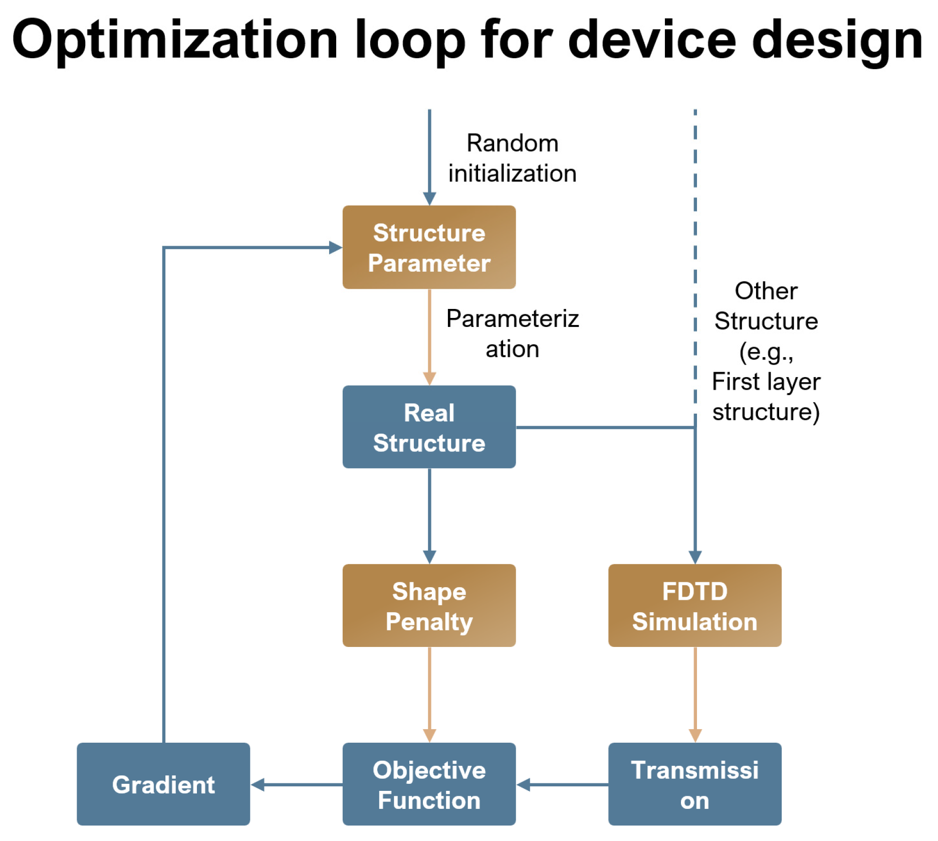
As shown in
Figure 1, the process works as follows. A random two-dimensional array is first generated as the initial design and then transformed into a physical structure through parameterization. The structure is then simulated using Tidy 3D FDTD analysis, and mode monitors are employed to evaluate the transmission at different output channels. Meanwhile, shape-penalty terms are computed to enforce geometric regularity. With these values, the objective function can be evaluated. Using gradient descent and adjoint sensitivity analysis, the structure is updated step by step according to the objective function [
15,
24]. By repeating this loop many times, the design gradually improves, and finally a device with good performance is obtained.
In the cascaded design, this optimization procedure is applied sequentially. The first-stage WDM unit is optimized independently and fixed. Based on this optimized structure, a second-stage WDM unit is trained to further separate the remaining wavelengths.
2.1. Objective Function
In the inverse design framework, the objective function defines the optimization target and directly influences both convergence behavior and final device performance. In this work, the objective function consists of two components: an optical performance term based on transmission and a smoothness constraint imposed on the device geometry.
To evaluate the optical performance, mode monitors are placed at the output ports of the device. These mode monitors are placed at the output ports of the device to measure the transmitted power at the target wavelengths. To promote balanced transmission among different output channels, the optical objective is formulated using the geometric mean of the transmission values:
where
is the transmission at the
i-th output port, measured by the mode monitor, and
N is the total number of output ports.
To ensure that the optimized device remains compatible with fabrication constraints, a radius-of-curvature penalty and an erosion-dilation penalty are introduced in addition to the transmission-based objective [
8,
25,
26].
The overall objective function combines the optical performance term and the penalties:
2.2. Design Parameterization
In inverse design, direct pixel-level optimization often leads to geometries that are difficult to fabricate [
27,
28]. For example, checkerboard structures often appear, and very small features may also show up. These small features can be expensive or difficult to realize in practice. To overcome this problem, we add a filtering step and a projection step in the parameterization process [
29].
A conic filter is applied to smooth the design region and suppress high-frequency spatial components. Following this filtering step, a hyperbolic tangent-based projection is employed to drive the continuous design variables closer to 0 or 1, thereby yielding a clearer material boundary between silicon and air. The mathematical form is written as:
In this formula,
is a parameter that controls the steepness of the projection, set to 30.
is the threshold, set to 0.5. By repeatedly applying the filtering and projection operations during optimization, the design variables gradually converge toward smooth and near-binary distributions. Finally, this distribution is mapped to a permittivity profile:
Here is the refractive index of silicon. The result is a structure that can be used directly in an FDTD simulation. More importantly, it avoids checkerboard artifacts, improves fabrication feasibility, and makes the optimization more stable.
2.3. Gradient Descent Method
After getting the parameterized representation of the device, the design variables are updated using a gradient-based method. Tidy3D provides adjoint sensitivity analysis, which makes it possible to calculate the gradient of the objective function with respect to all design parameters in an efficient way [
15,
23]:
The resulting gradient information is used to update the design variables through an iterative optimization scheme:
where
is the learning rate.
The optimization is carried out with JAX + Optax (Adam). The learning rate is set to 0.2, with 100 iterations.
2.4. Performance Metrics
To evaluate the device, several performance metrics are defined. These metrics describe how much power is transmitted and how well the device suppresses unwanted channels.
The transmission coefficient of port
k at wavelength
λ is defined as:
Here, is the output power carried by the desired mode at port , and is the input modal power. This metric characterizes the coupling efficiency into each output channel.
Crosstalk describes how much unwanted power from other channels leaks into the channel of interest. It is defined as:
In this expression, the numerator represents the total transmitted power except for the desired one, and the denominator is the power of the target channel. Lower crosstalk values indicate improved channel isolation.
3. Results
In this work, a single-input, three-output cascaded WDM device is designed and optimized for wavelength demultiplexing. The device operates by separating three target wavelengths (1450 nm, 1500 nm, and 1550 nm) into distinct output ports using a two-stage cascaded architecture. Related cascaded digital-metamaterial devices have shown that cascading individually designed functional regions can support compact high-dimensional demultiplexing. In the first stage, the 1450 nm wavelength is routed to the top output port, while the remaining wavelengths propagate to the subsequent stage. The second stage further demultiplexes the 1500 nm and 1550 nm signals into the middle and bottom output ports, respectively.
Prior to device optimization, a modal analysis is performed for the input waveguide (
Appendix A.1). The computed eigenmodes indicate that the waveguide supports multiple guided modes within the wavelength range of interest.. In the present waveguide configuration, the selected fundamental mode corresponds to mode index 0 and is TM-like, with the electric field predominantly oriented along the
component. The effective index of the fundamental mode decreases slightly from 3.0836 at 1450 nm to 3.0446 at 1550 nm, confirming that there remains strong optical confinement over the wavelength range considered. This fundamental mode is used for both excitation and transmission evaluation in subsequent simulations.
In integrated waveguides, the guided modes are generally not purely TE or TM, but are commonly described as TE-like or TM-like modes according to their dominant field components. The proposed inverse-design framework itself is not restricted to TM-like operation; it can also be extended to TE-like modes by redefining the source mode and the target modes used in the output mode monitors.
3.1. First Stage Results of the Cascaded Design
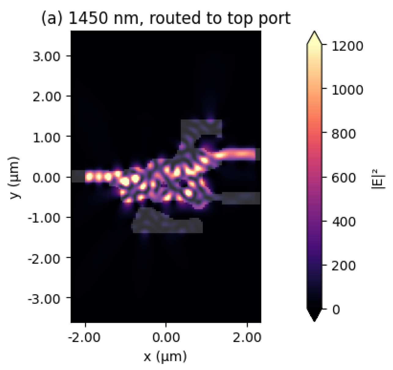
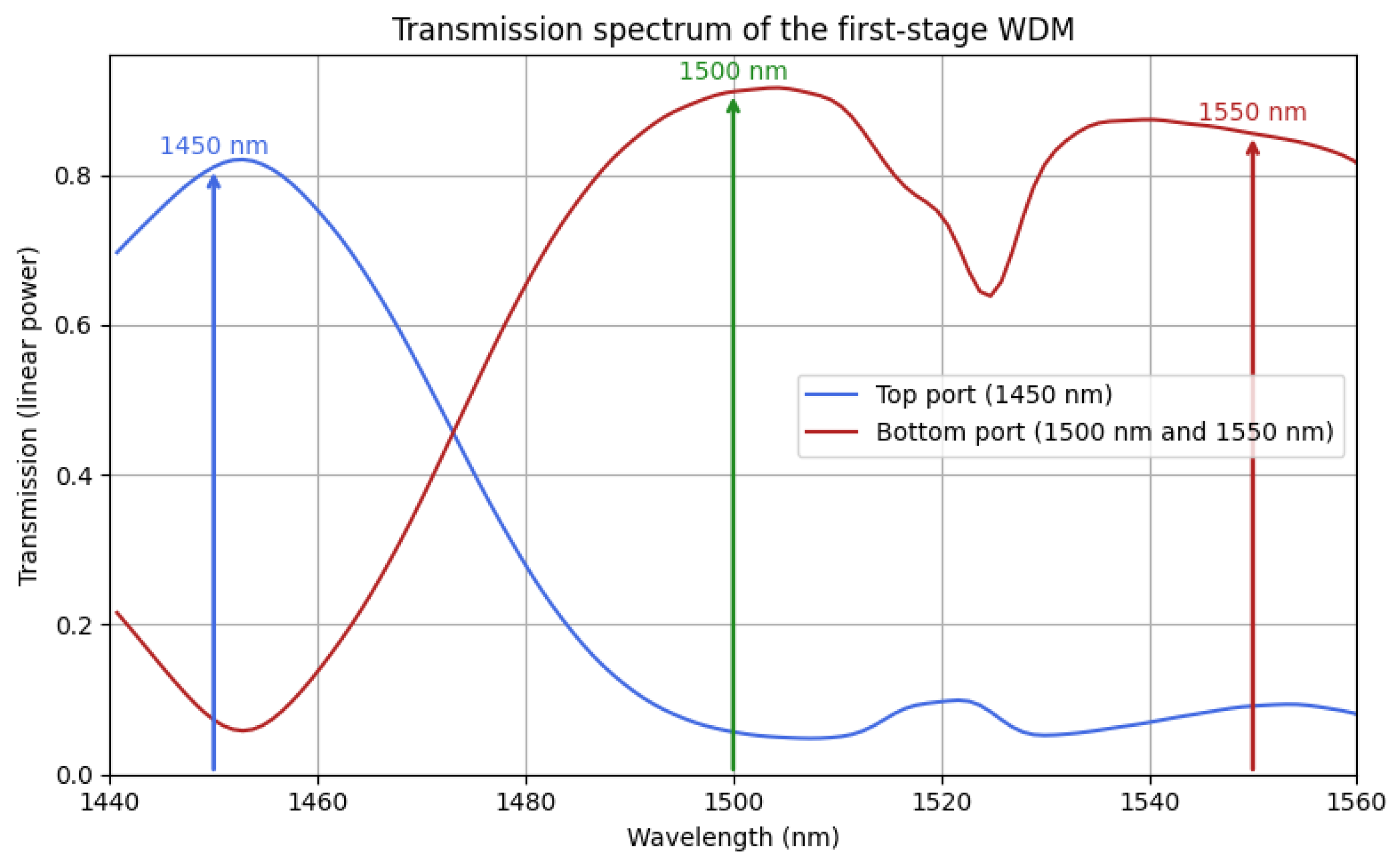
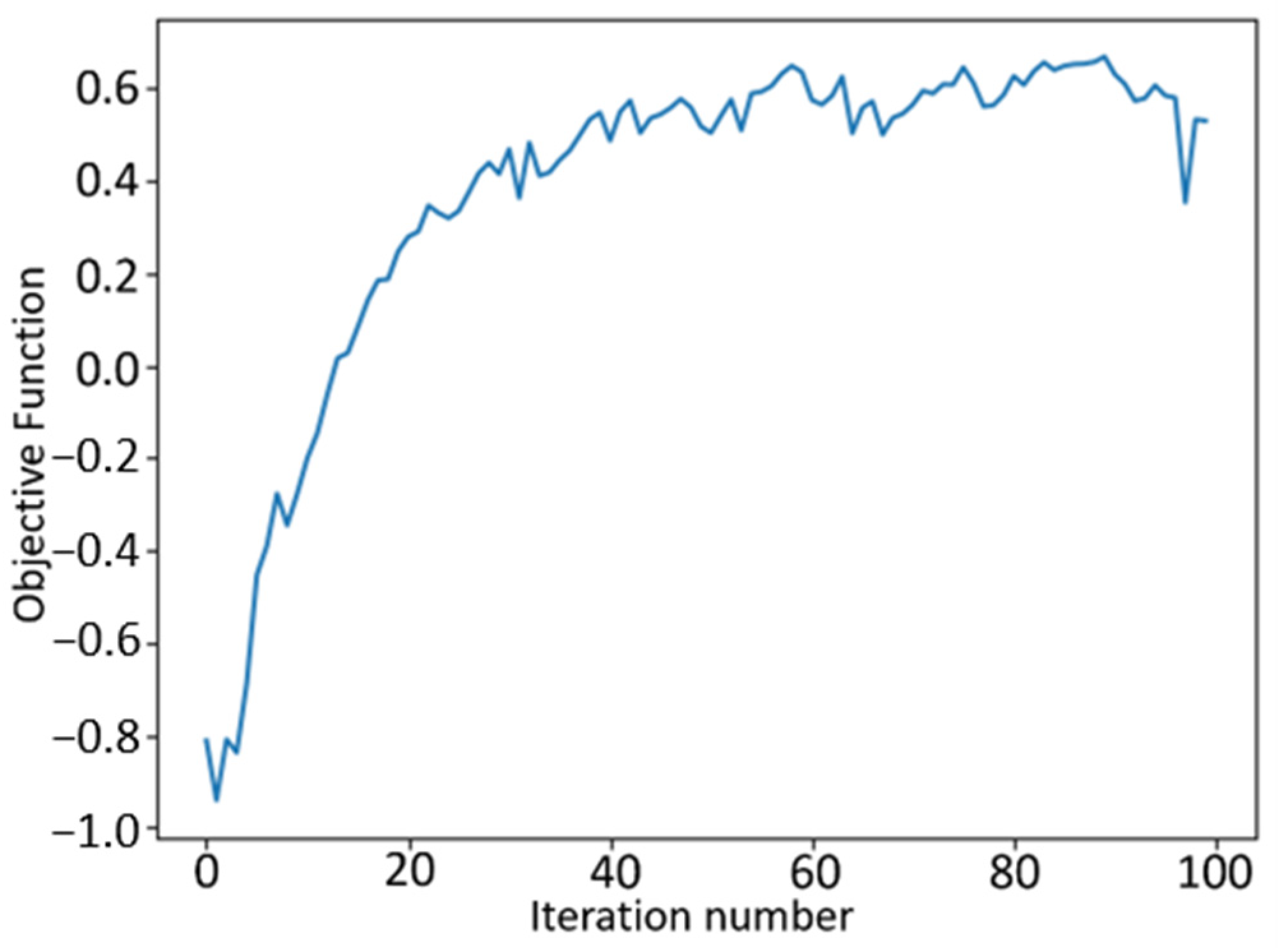
The results of the two-port first-stage WDM are presented in
Figure 2,
Figure 3 and
Figure 4. The optimized structure exhibits wavelength-selective routing with the 1450 nm signal guided to the top output port and the 1500 nm and 1550 nm wavelengths propagating to the bottom waveguide port.
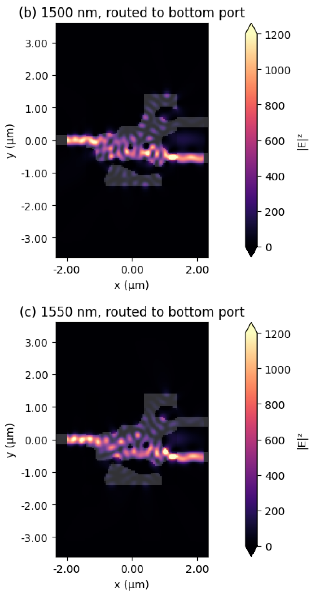
Figure 2 shows the electric field intensity at the three target wavelengths. The 1450 nm signal is clearly directed into the top port, while 1500 nm and 1550 nm are guided into the bottom ports. This validates the effectiveness of the first stage and also prepares a proper input condition for the second stage.
Figure 3 shows the transmission spectrum for the three target wavelengths. Again, the 1450 nm input couples mainly to the top port, while the 1500 nm and 1550 nm inputs continue to the bottom port so that the remaining two target wavelengths are directed downward after this first splitting stage. Away from these wavelengths, the transmissions are below 0.1, showing that unwanted leakage into the wrong ports is largely suppressed. This confirms that the first stage already performs a coarse wavelength separation, sending 1450 nm upward and leaving the longer wavelengths for the second stage to process. The transmission results confirm that the first stage performs efficient wavelength separation.
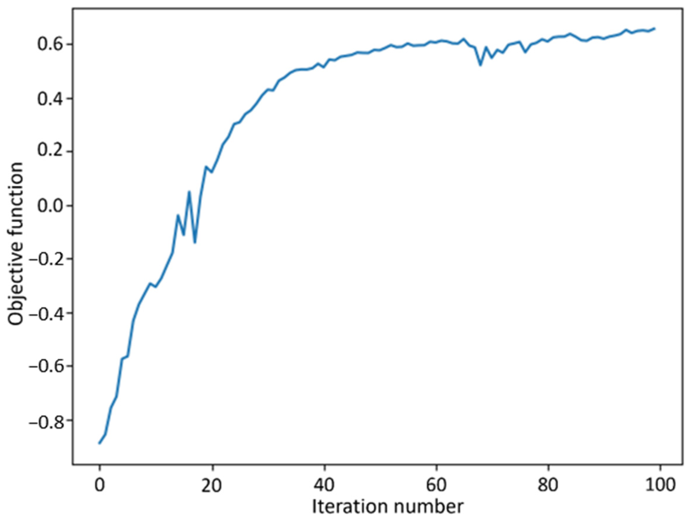
Figure 4 shows the objective function evolution during the optimization of the first-stage WDM unit. The objective function increases rapidly in the early iterations and gradually converges after about 40 iterations, with only minor fluctuations, demonstrating the robustness of the first-stage optimization.
3.2. Results of the Cascaded WDM
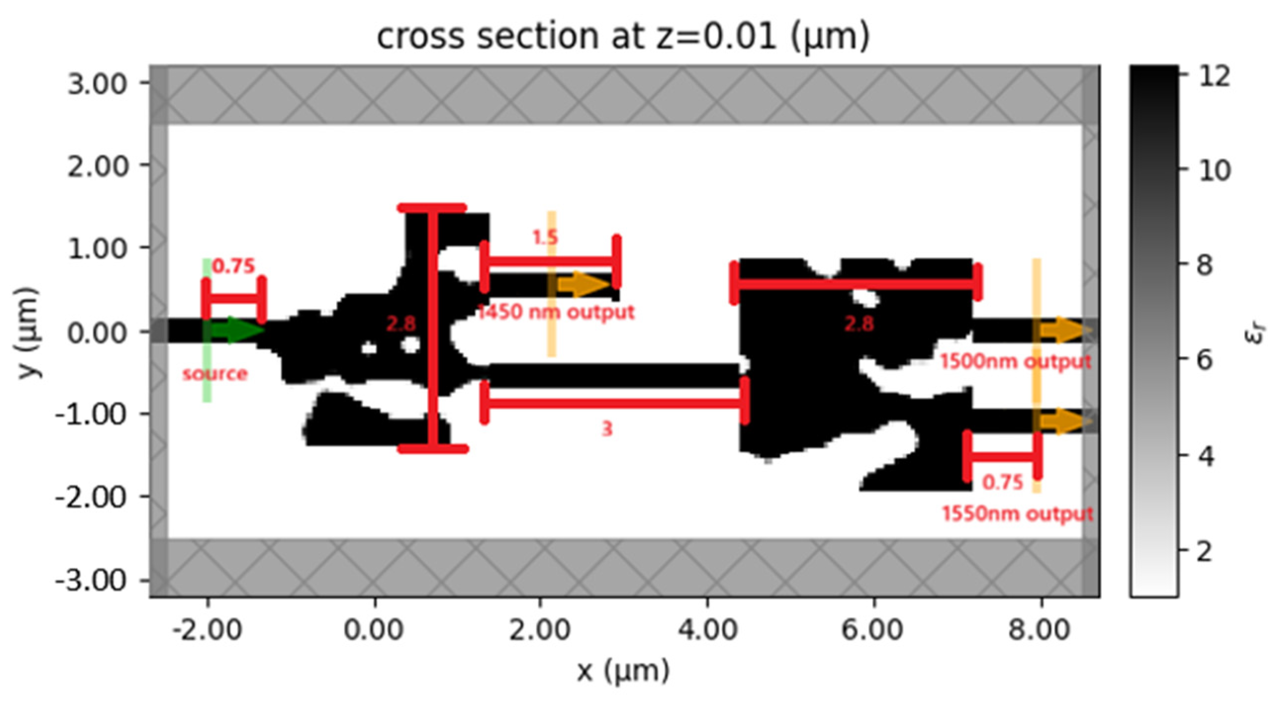
The in-plane layout of the proposed cascaded WDM is shown in
Figure 5. The black regions represent silicon, and the white background represents air. The green arrow indicates the input source and its propagation direction, while the orange arrows indicate the output mode monitors and their detection directions. The main dimensions of the input/output waveguides, inverse-designed regions, and connecting waveguide are labelled in microns.
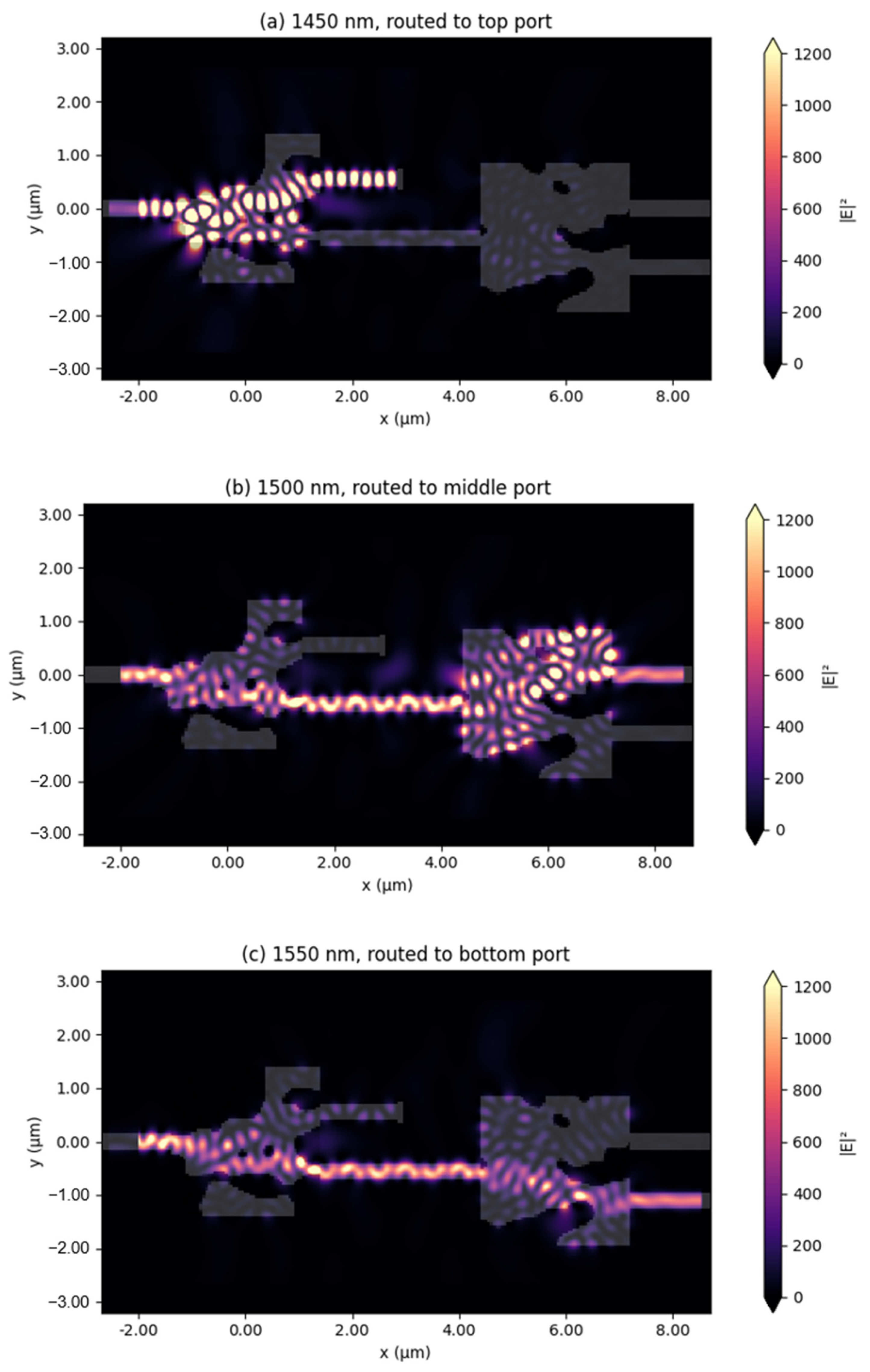
The performance of the 2-stage cascaded WDM device is presented in
Figure 6,
Figure 7 and
Figure 8 and summarized quantitatively in
Table 1. By connecting two optimized two-output stages in series, the cascaded structure enables single-input, three-output wavelength demultiplexing within a compact footprint.
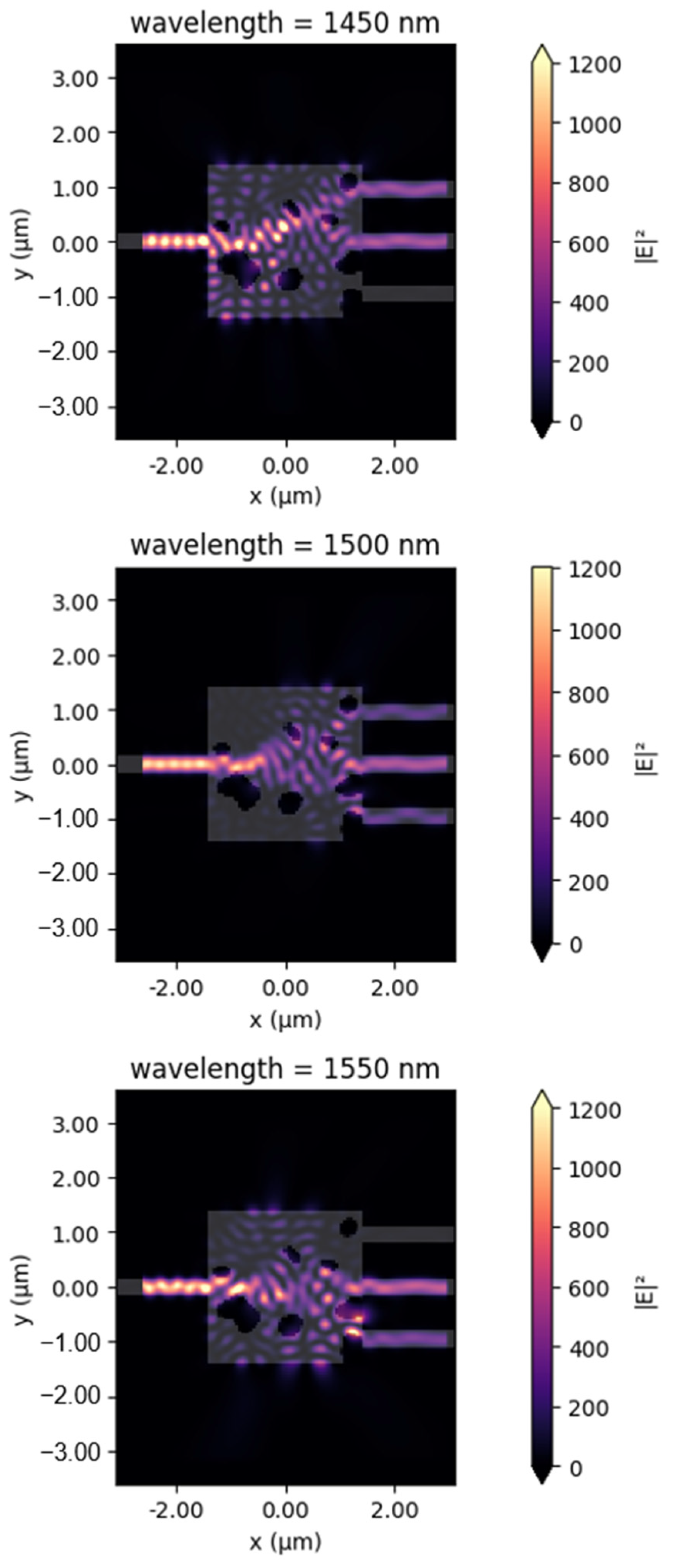
Figure 6 shows the electric field distributions at the three wavelengths. The results confirm that the cascaded device achieves single-input, three-output wavelength demultiplexing. We observe that, compared with the first stage, the 1450 nm wavelength exhibits greater leakage into the middle and bottom channels, whereas the 1550 nm wavelength leaks into the top channel. This is due to the fact that the right side of the domain cell is terminated by a PML boundary during the training of the first stage. However, the first stage is connected to a real load in the final cascaded training, which changes the simulation environment.
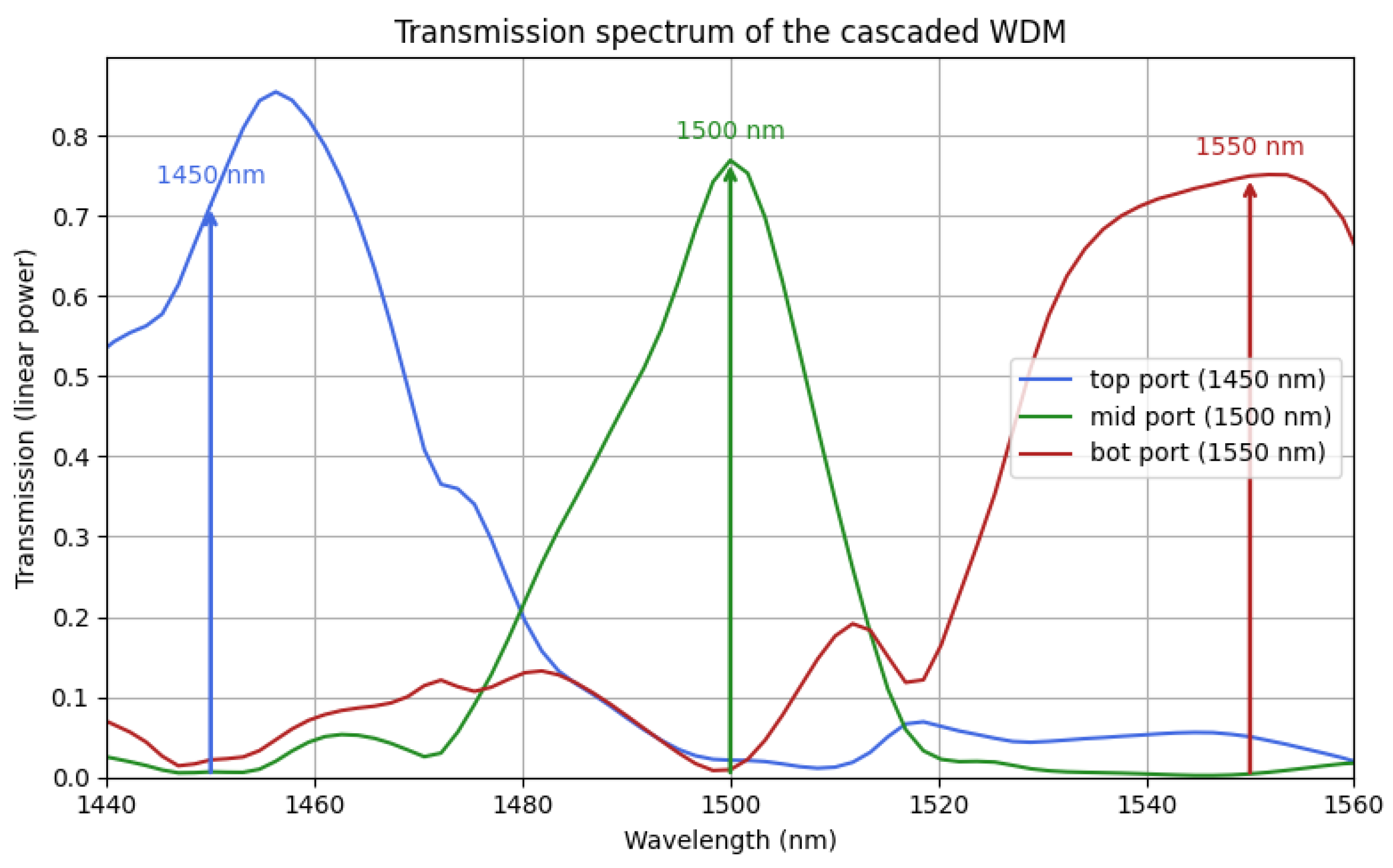
Figure 7 shows the transmission spectrum of the cascaded WDM. The spectrum shows that each port has a clear peak near the wavelength it is expected to handle. The top port peaks around 1450 nm, the middle port peaks around 1500 nm, and the bottom port peaks around 1550 nm. The three target wavelengths are separated and enter the correct channels.
The peak transmission is greater than 0.7. When the wavelength is far from the target wavelength, the signal at each port will drop rapidly below 0.1. This drop indicates that most of the unwanted power will not leak to the wrong port, so the crosstalk is much lower compared to the previous single-stage situation.
Figure 8 shows the objective function evolution during the second-stage optimization. Similar to the first-stage training, the objective function increases rapidly in the early iterations and reaches a converged regime after approximately 50 iterations. Although larger fluctuations are observed due to the increased structural complexity and interaction with the fixed first-stage unit, the optimization remains stable overall, confirming the effectiveness of the cascaded training strategy.
Overall, the cascading design work is reasonable. It achieves the separation of three channels, and the isolation degree between the channels is within an acceptable range. The spectrum is not perfect, and there will still be some fluctuations, making the curve look a bit chaotic. But importantly, the concept itself has already been verified. By dividing tasks into smaller stages rather than attempting to solve all problems in one stage, the optimization process becomes more stable.
As shown in
Table 1, the cascaded WDM significantly reduces crosstalk across all ports compared to the single-stage WDM.
To benchmark the proposed cascaded WDM against representative compact and inverse-designed wavelength demultiplexers,
Table 2 summarizes the number of channels, wavelength spacing, footprint, validation method, insertion loss or transmission, and crosstalk or extinction-ratio values reported in the literature. The present design achieves simulated three-channel routing within a 17.745 μm
2 footprint, with a minimum target-port transmission above 0.71, corresponding to an insertion loss below approximately 1.5 dB, and crosstalk below −9.97 dB. Compared with the experimentally demonstrated three-channel demultiplexer by Su et al. [
18], the proposed cascaded device is smaller while maintaining a comparable simulated insertion-loss level; however, its crosstalk is weaker than recent low-crosstalk reports that use photonic-crystal filtering or SWG/MMI-assisted designs [
19,
30,
31,
32]. Thus, the main contribution of the present work is not a record crosstalk value, but a compact cascaded inverse-design strategy that simplifies the three-output optimization problem. This comparison also identifies the most important improvements needed for a stronger publication case: fabrication-tolerance analysis, measured spectra, and additional crosstalk-suppression stages.
4. Discussion
The first stage effectively separates the three wavelengths at 1450, 1500, and 1550 nm in the desired directions: the transmission of all three channels is above 0.8.
After adding the second stage, the transmission of the three output channels generally decreases by approximately 0.1. For the middle and bottom output ports, this is because the light, passing through the second stage, experiences scattering losses similar to those in the first stage. This loss results in a transmission drop of approximately 0.13 per waveguide stage. This is verified by simulation, with transmission generally decreases by approximately 0.16 upon passing through the first stage. When passing through the second stage, the transmission generally decreases by approximately 0.1. These results indicate that scattering loss accumulates as additional stages are introduced. As a result, the reduction in transmission becomes a key factor limiting the scalability of cascaded WDM architecture, particularly when extending to a larger number of stages.
For the top output port, although it experiences scattering loss once, the structure’s shape indicates that the straight waveguide between the two stages inadvertently forms an equivalent Fabry–Perot cavity with the devices on both sides. This causes the incident light to reflect back and forth between the two surfaces, resulting in multiple interference effects. The output exhibits transmission peaks and suppression bands, with periodic spectral distribution and interference enhancement or reduction at specific wavelengths. This is why the transmission spectrum of the first stage appears smoother, while that of the second stage appears undulating. This is often a side effect in cascaded WDM systems, resulting in reduced transmission, intra-band ripple, and inter-channel crosstalk.
These conditions are also related to the load change after the second stage is added. In the first stage of training, the right side is the PML. After cascading, the right side is replaced by the “real structure” of the second stage. Under the training environment of the first stage, the first stage will no longer be optimal after the second stage is added. This situation is almost unavoidable because the training process requires a specific order. If the second stage is trained first, the correct input of the intermediate coupled waveguide cannot be used. If trained simultaneously, the result is equivalent to designing a single-input, three-output waveguide over a larger area. In this case, the inverse design optimization process is often unstable, and the objective function has difficulty converging to a suitable value.
Although the effective refractive indices of the two trainings are almost identical in this simulation, interface mode-field mismatch is also a consideration in cascaded WDM designs. This is manifested in the fact that the “actual output field” of each stage is not necessarily equal to the “target fundamental mode” of the next stage, and some of them are coupled to higher-order or radiative modes. While this mismatch becomes more noticeable as the number of cascaded stages increases, its impact is generally less significant than the transmission loss introduced by additional inverse-designed regions.
Compared with the single-stage design, the cascaded structure only needs to deal with two channels at each stage. The objective function is therefore simpler, and the optimization converges faster and more stably. A single-stage device with three or more outputs is essentially a high-dimensional multi-objective problem, as also noted in prior three-channel inverse-designed demultiplexer work [
16]. The cascaded structure breaks this down into smaller parts, reducing the parameter space and making it easier for the optimizer to find a solution. Since each stage only performs a two-way split, the crosstalk is also greatly reduced.
Building upon this training framework, the cascaded architecture may be further extended to support a larger number of output channels and a broader operating wavelength range. Hierarchical cascading topologies, such as tree-based architectures, could be explored to improve scalability while limiting cumulative transmission loss and inter-channel crosstalk. In addition, incorporating fabrication tolerance analysis is essential to enhancing the robustness and manufacturability of large-scale cascaded WDM designs.
Previous WDM and triplexer devices have been demonstrated using directional couplers, MMIs, MMRs and AWGs [
33]. These approaches have achieved important advantages, including low insertion loss, experimentally verified operation, polarization-insensitive designs, and mature access-network implementations. However, many of them rely on predefined wavelength-routing mechanisms, such as self-imaging, resonance, phase matching, or grating diffraction, and their device dimensions are often constrained by these physical principles [
34,
35,
36,
37]. In contrast, inverse design provides a more flexible route by directly searching for compact wavelength-routing geometries according to the desired optical response.
Compared with these conventional approaches, the present cascaded inverse-designed WDM provides a more compact and flexible design route. Instead of relying on a specific analytical wavelength-routing mechanism, such as self-imaging, resonance, phase matching, or grating diffraction, the device geometry is directly optimized according to the desired output transmission objectives. This allows non-intuitive scattering structures to be formed within a very small design region.
Nevertheless, several limitations remain. First, the present work is based on two-dimensional numerical simulations using a silicon-in-air model. Explicit substrate, buried oxide, and top-cladding layers are not included, and therefore, a full three-dimensional SOI implementation should be investigated in future work. Second, the current study focuses on simulated optical performance, and neither fabrication nor experimental transmission measurements have yet been carried out. Third, fabrication tolerance, sidewall roughness, minimum feature-size constraints, and polarization dependence require further analysis before practical implementation.
5. Conclusions
This work investigated the challenges of inverse-designed multi-output wavelength division multiplexers on silicon, where direct single-stage optimization often suffers from unstable convergence and severe inter-channel crosstalk, especially under compact footprint constraints. To address these limitations, a cascaded inverse design strategy was proposed, in which the multi-output demultiplexing task is decomposed into a sequence of two-output WDM stages optimized sequentially.
Using a full-wave FDTD and adjoint-based optimization framework, we designed and analyzed a single-input, three-output cascaded WDM device. Numerical results demonstrate that the proposed cascaded architecture successfully routes three target wavelengths at 1450 nm, 1500 nm, and 1550 nm into distinct output ports, achieving a minimum transmission exceeding 0.71 and inter-channel crosstalk below −9.97 dB within a compact footprint of 17.745 μm2. Compared with direct single-stage multi-output designs, the cascaded approach exhibits improved optimization stability and reduced channel competition, at the cost of moderate transmission degradation due to additional cascading.
Overall, this study shows that cascaded inverse design provides a practical and scalable pathway for realizing compact multi-channel WDM devices on silicon photonic platforms. While the present device does not yet replace experimentally demonstrated conventional triplexer technologies, it demonstrates the potential of inverse design to compress multi-wavelength routing functions into an ultra-compact footprint and to provide additional design flexibility for future integrated photonic WDM systems.