


Abstract
The development of quantum computers presents a great challenge for current cryptographic algorithms. Post-quantum cryptography has been proposed to secure against quantum computers in the near future. Modular polynomial multiplication is a frequent arithmetic operation in post-quantum cryptography. In this paper, a low-cost and efficient pipelined architecture for modular polynomial multiplication in Saber has been proposed and synthesized with the Virtex UltraScale + xcu200-fsgd2104-2-e board. It can achieve a frequency of 250 MHz and only uses 11,499 LUTs, 7034 FFs and 32 IOs.
1. Introduction
Research on large-scale quantum computers has increased recently [1]. IBM Quantum and UC Berkeley experimented with the IBM Quantum “Eagle” 127 qubits quantum processor and demonstrated that a quantum computer could outperform leading classical simulations by learning and mitigating errors in the system and by measuring accurate expectation values for circuit volumes at a scale beyond brute-force classical computation [2,3,4]. Google Quantum AI used the Sycamore quantum processor and determined the conditions under which quantum computers can outperform classical supercomputers [5,6]. The development of quantum computers presents a great challenge for current cryptographic algorithms used for information and communication security. The mathematical problems behind those cryptographic algorithms such as RSA and ECC could be easily solved with quantum computers in the near future. Post-quantum cryptography (also called quantum-resistant cryptography) has been proposed to secure against quantum computers. The NIST published three post-quantum cryptography standards FIPS 203, FIPS 204 and FIPS 205, which derived from CRYSTALS-Dilithium, CRYSTALS-KYBER and SPHINCS+ on 13 August 2024 [7,8,9].
Lattice-based cryptography has been applied in quantum-resistant cryptographic algorithms such as Kyber [10] and Saber [11], which are based on the difficulty of solving the learning-with-errors (LWE) problem over module lattices. The most frequent arithmetic operation used in lattice-based cryptography is modular polynomial multiplication. For example, the polynomial ring Rq in Kyber is represented by Zq[X]/(Xn + 1), where n = 256 and q = 3329. A similar polynomial ring, Rq, is used in Saber except q = 213. Feng et al. proposed a multi-lane NTT (number theoretic transform) algorithm with a customized memory-addressing strategy and round constant managing scheme to speed up the modular polynomial multiplication [12]. Li et al. proposed a reconfigurable modular polynomial multiplier with the butterfly unit (BU) structure, which was composed of modular addition, subtraction and multiplication [13]. A parallelized NTT-based modular polynomial multiplier was presented in [14] to support lattice-based homomorphic cryptographic schemes.
However, NTT-like polynomial multiplication cannot be applied in Saber due to its use of the two-power moduli (q = 213) [11]. Tan et al. proposed a Karatsuba-based modular polynomial multiplier with the fast finite-impulse-response (FIR) filter architecture and extended it to fast M-parallel architectures [15]. A high-throughput parallel and scalable schoolbook polynomial multiplier was proposed by unrolling the inner loop of the schoolbook polynomial multiplication with a highly parallel pipelined structure (maximum eight parallel cores) in [16]. Its minimum costs were 47,654 LUTs, 23,872 FFs and 1 BRAM in the Virtex UltraScale + FPGA board. Zhu et al. proposed a crypto-processor LWRpro, which applied an eight-level recursive split hierarchical framework to reduce degree-256 polynomial multiplication to coefficient-wise multiplication [17]. A domain-specific co-processor, which distributed computing at the micro-architectural level for polynomial multiplication in Saber, was proposed in [18]. Wong et al. proposed a four-layer hierarchical Karatsuba polynomial multiplier with degree-16 sub-polynomials computed by schoolbook polynomial multiplication and implemented on a Xilinx Zynq UltraScale + FPGA (ZCU102) [19]. A parallel polynomial multiplier was proposed and applied in the instruction-set co-processor architecture for lattice-based cryptography (Saber as a case study) with the implementation on Xilinx UltraScale + XCZU9EG-2FFVB1156 FPGA [20]. Other post-quantum cryptography algorithms like FrodoKEM [21], NTS-KEM [22], NewHope [23] and NTRU [24] also use polynomial multiplications as the core operation.
In this paper, a cost-efficient pipelined architecture for modular polynomial multiplication is proposed. The contributions of the proposed polynomial multiplier are the following:
- (1)
- Serial input and serial output (SISO): The coefficients of two polynomials are input serially. One coefficient of the multiplicand and one coefficient of the multiplier are input simultaneously by one clock cycle. The coefficient of the product is output serially. The first coefficient of the product will be generated and output after 256 clock cycles (n = 256). The input pins and output pins are reduced dramatically with SISO.
- (2)
- Simple process element (PE) design: Each PE only includes two arithmetic operations: modular addition and modular multiplication, except the first PE, which only performs modular multiplication. In total, 256 simple PEs are required in the architecture. The PEs are repeatedly used to calculate the partial product to save hardware cost.
- (3)
- Pipelined architecture: The product coefficient will be generated through the pipelined architecture. In total, 256 clock cycles are needed to generate all the product coefficients.
- (4)
- Cost-efficient design: The proposed architecture has been synthesized with the target on a Virtex UltraScale + xcu200-fsgd2104-2-e board. It only costs 11,499 LUTs, 7034 FFs and 32 IOs. The number of equivalent slices and the product of area and latency have been reduced dramatically compared to the previous designs.
2. Cost-Efficient Pipelined Architecture for Modular Polynomial Multiplication
The modular polynomial multiplication a(x) s(x) mod (x8 + 1) is used as an example to illustrate the design. Suppose a(x) = a7x7 + … + a1x + a0, s(x) = s7x7 + … + s1x + s0, Table 1 demonstrates the polynomial multiplication of a(x) s(x) with the schoolbook algorithm. The sum of each column will be the coefficient of the product.
Table 1.
Polynomial multiplication of a(x) s(x), a(x) = a7x7 + … + a1x + a0, s(x) = s7x7 + … + s1x + s0.
In the modular polynomial multiplication a(x) s(x) mod (x8 + 1), we can derive the following:
x14 mod (x8 + 1) = x14 − x6 (x8 + 1) = −x6
x13 mod (x8 + 1) = x13 − x5 (x8 + 1) = −x5
…
x9 mod (x8 + 1) = x9 − x (x8 + 1) = −x
x8 mod (x8 + 1) = x8 − (x8 + 1) = −1
Table 2 illustrates the modular polynomial multiplication a(x) s(x) mod (x8 + 1). The sum of each column will be the coefficient of the modular product.
Table 2.
Modular polynomial multiplication of a(x) s(x) mod (x8 + 1), a(x) = a7x7 + … + a1x + a0, s(x) = s7x7 + … + s1x + s0.
In Table 2, the coefficients of a(x) are in an order from a0 to a7 in each column. In each row, the coefficient of s(x) is the same. The order of the coefficients of s(x) from each row are s7, s6, s5, s4, s3, s2, s1, s0, −s7, −s6, −s5, −s4, −s3, −s2, −s1. One column of the clock cycle is included in the table. The modular polynomial multiplication of a(x) s(x) can be easily implemented with pipelined PEs and shift registers to store the coefficients of s(x). The product of coefficients aisj in each row are the multiplications in each clock. Each PE includes a modular multiplier and a modular adder/subtractor. Algorithm 1 is the proposed algorithm for serial-input serial-output pipelined modular polynomial multiplier.
| Algorithm 1 Serial-input serial-output pipelined modular polynomial multiplier |
| Input: s[255:0] 4 bit array, a[255:0] 13 bit array, clock, reset Output: p[255:0] p = a(x) s(x) mod (x256 + 1) // SR[256:0] Shifter Registers, R[255:0] Register, PR[255:0] Pipeline Registers If Reset SR[256:0] = 0, R[255:0] = 0; Else At each clock cycle, do {Input one coefficient of s(x) (beginning from MSB) to SR[0]; Input one coefficient of a(x) (beginning from LSB) to the specified location of R; Shift SR to right by 4 bits; If (clock counter > 256) m_output = −SR[256]; // change the sign of SR[256] Else m_output = SR[0]; PE[0] = m_output * R[0] mod q; PR[0] = PE[0]; For (i = 1; i < 256; i++) { PE[i] = (m_output * R[i] + PE[i − 1]) mod q; PR[i] = PE[i] } } Output p[j] = PR[255] serially after 256 clock cycles (j is from 255 to 0, MSB of p(x) output first) |
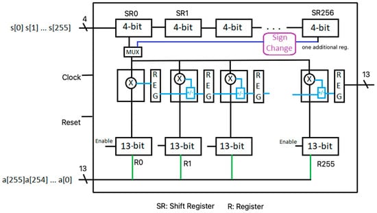
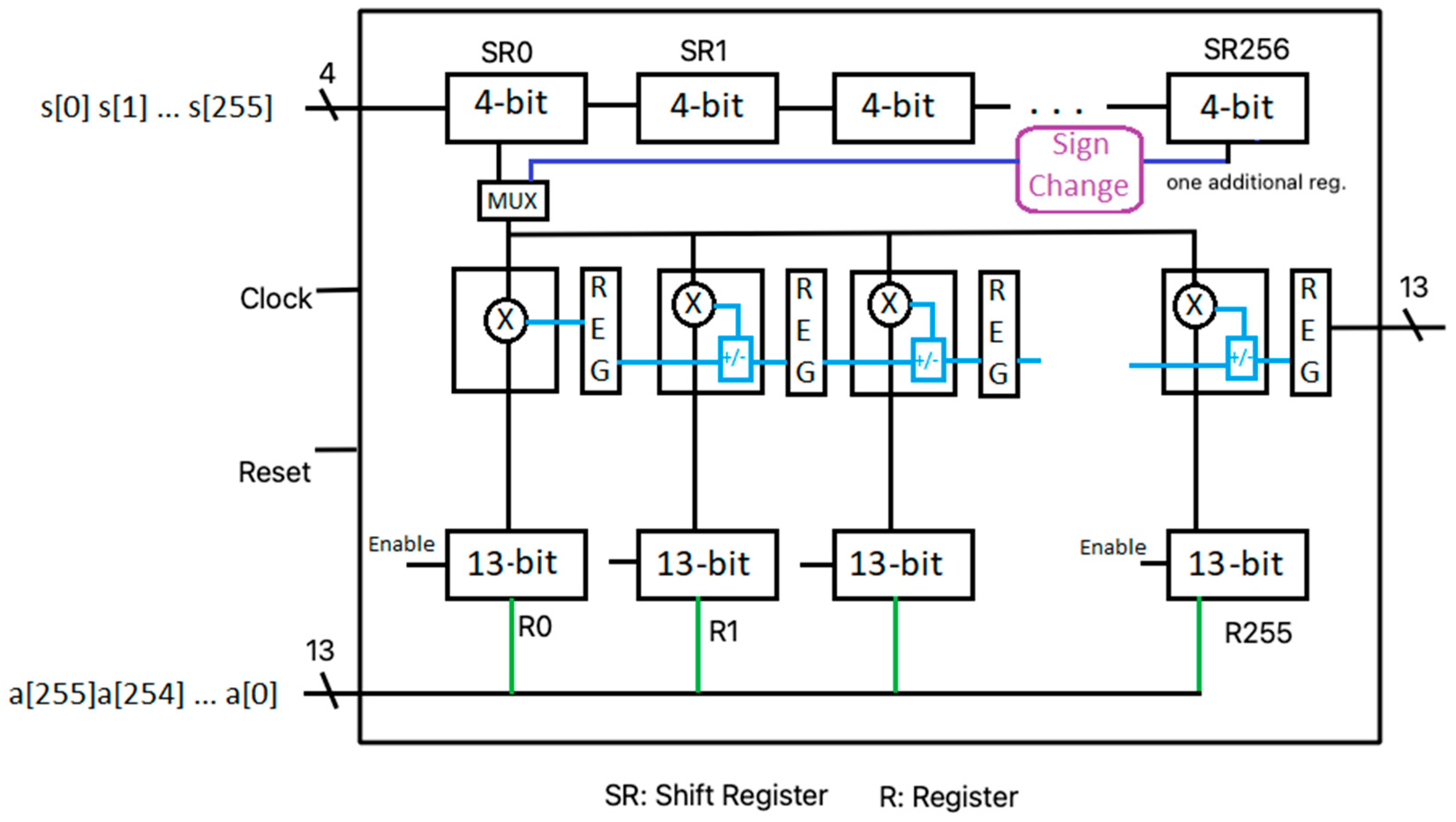
Figure 1 illustrates the proposed architecture. The top-row registers are 256 shifter registers to store the coefficients of s(x), which are input serially starting from the most significant coefficient s[255]. One additional register SR[256] is added at the end to store the shifted coefficients from the previous register. The coefficient shifted into this last register needs a sign-change operation.
Figure 1.
The proposed cost-efficient SISO pipelined modular polynomial multiplier.
The multiplexer is controlled by a clock counter.
The output of the multiplexer is as follows:
If clock counter > 256 output = the result of sign-change operation
else output = Register SR[0]
The bottom-row registers store the coefficients of a(x), which can also be input serially starting from the least significant coefficient a[0] to save on the number of input ports. A counter of the clock cycles is required to enable the register to receive the serial-input coefficient on the specified clock cycle.
In Saber, the modular polynomial multiplication is expressed as a(x) s(x) mod x256 + 1, where the coefficient of a(x) is 13 bits; the coefficient of s(x) is the secret coefficient in the range of [−5, 5] for LightSaber, [−4, 4] for Saber and [−3, 3] for FireSaber [11]. The coefficients of s(x) are serially input to a group of 4 bit shift registers beginning with the most significant bit (s[255]). The coefficient of a(x) is also serially input to another group of registers beginning with the least significant bit (a[0]). Those registers are controlled by enable signals. In the first clock, a[0] is input to the left-most register, a[1] is input to the second register in the second clock, and so on. After 256 clocks, the coefficient in the last 4 bit register will go through a function of sign change. The output of the sign change will be the input for each PE in the architecture. In the meantime, MUX will select the second input as the output after 256 clocks. Also, the shifting registers continue working, that is, the register SR[254] will be shifted to the last register.
For the modular polynomial multiplication in Zq[X]/(Xn + 1), the proposed algorithm can be implemented with a multiplexer, a sign-change module, n + 1 4-bit shift registers, 2n 13-bit registers and n PEs. Each PE includes one modular multiplier (ai × sj mod q), and one adder/subtractor, except the first PE, which only includes one modular multiplier. It takes n clock cycles to generate all the product coefficients.
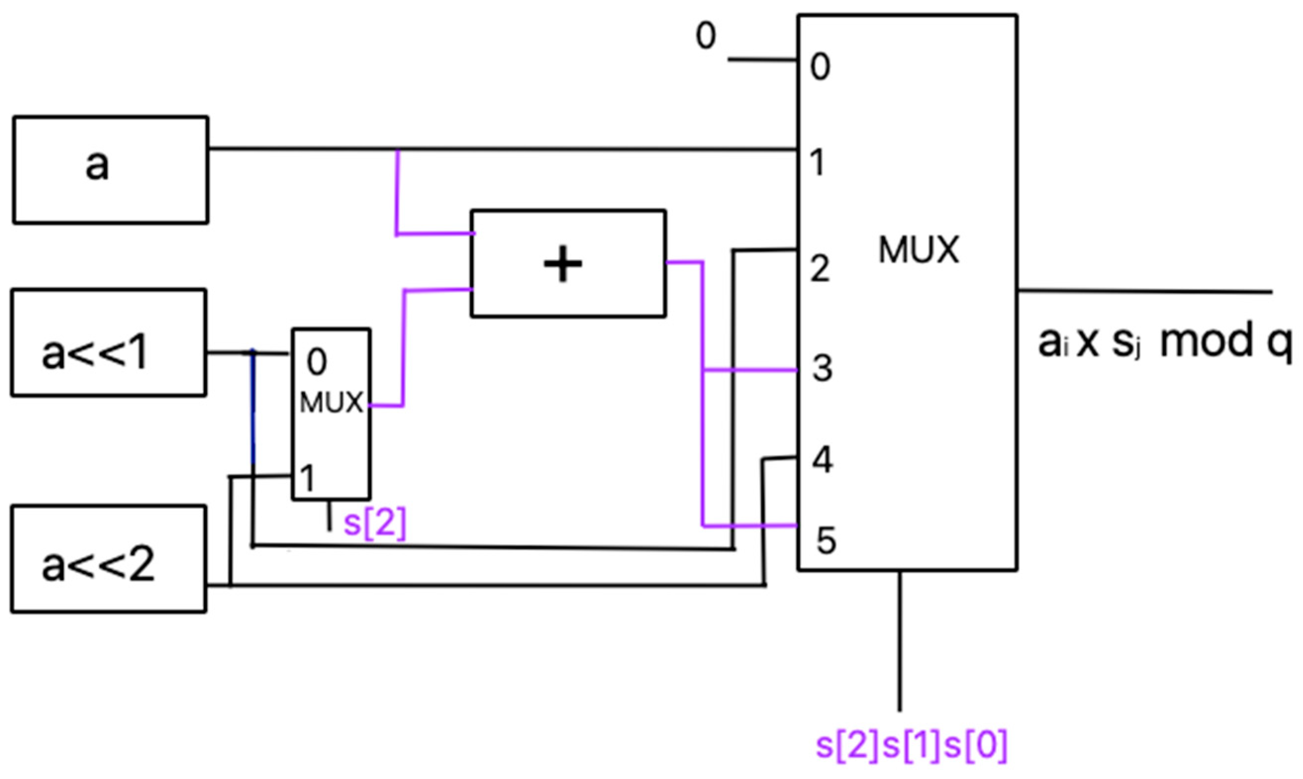
The modulus in Saber is the power of 2 (q = 213), which is very easily implemented with the bitwise logical “and” operation. The modular multiplication algorithm (Algorithm 2) proposed by Roy and Basso [20] is applied, and one more output is added in the proposed design to control the modular addition/subtraction. The coefficient of s(x) is represented with a 4 bit sign-magnitude number, that is, s[3] is the sign bit (0: positive, 1: negative) and s[2]s[1]s[0] is the absolute value of the coefficient.
| Algorithm 2 Modular multiplier [20] |
| Input: a: 13 bit number, s: 4 bit sign-magnitude number with s[3] as the sign bit and the following bits as the absolute value of s Output: a · s modulo q, s[3]. r0 = 0 r1 = a, r2 = a << 1, r3 = a + r2, r4 = r2 << 1 r5 = a + r2 reurn r_k and s[3], where k = s[2]s[1]s[0] |
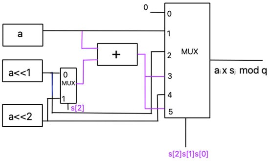
s[3] will be connected to the initial carry c_0 of the adder/subtractor. If s[3] = 0, then addition is performed. If s[3] = 1, then subtraction is performed. Figure 2 illustrates the logic diagram for ai × sj mod q.
Figure 2.
The logic diagram for ai × sj mod q.
3. Performance and Comparison
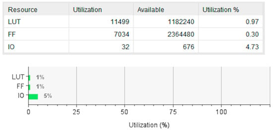
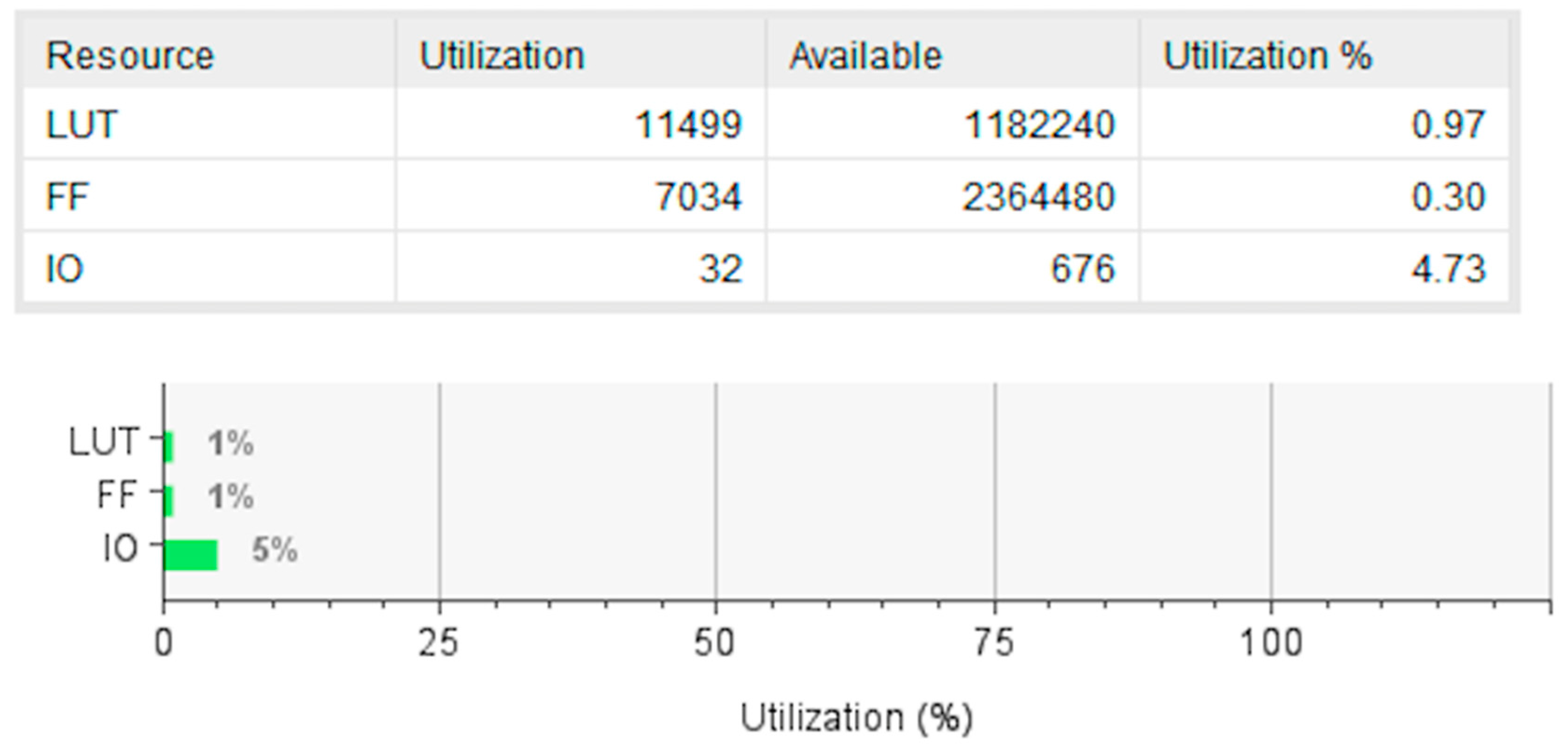
The proposed low-cost and efficient pipelined modular polynomial multiplier for Saber has been synthesized with the AMD Vivado Design Suite on the target of the Virtex UltraScale + xcu200-fsgd2104-2-e board. It can achieve a frequency of 250 MHz and only uses 11,499 LUTs, 7034 FFs and 32 IOs. Figure 3 is the utilization report.
Figure 3.
Synthesis utilization report (Virtex UltraScale + xcu200-fsgd2104-2-e board).
Each PE has the same structure, which includes one modular multiplier (ai × sj mod q) and one adder/subtractor, except the first PE, which includes only one modular multiplier. This simple PE design can decrease the delay of the critical path. Also, those PEs run in parallel and are repeatedly used at each clock to reduce the hardware resources.
The performance comparison with the previous designs is illustrated in the following Table 3. The number of equivalent slices is used for a fair comparison. It can be seen that the proposed design achieves the least number of equivalent slices and the least ATP (the product of Area and Latency).
Table 3.
Performance comparison.
4. Conclusions
Post-quantum cryptography has been proposed to secure against the near-future large-scale quantum computers. In this paper, a low-cost and efficient pipelined serial-in serial-out modular polynomial multiplier in Saber has been proposed and synthesized with a Virtex UltraScale + xcu200-fsgd2104-2-e board. The total number of LUTs and FFs decreased dramatically compared with that in previous work. The proposed multiplier can be embedded in the post-quantum crypto-processor for Saber and improve the processing speed and throughput to provide security services in the era of quantum computing.
Funding
This research received no external funding.
Data Availability Statement
The original contributions presented in this study are included in the article. Further inquiries can be directed to the corresponding author.
Conflicts of Interest
The author declares no conflict of interest.
References
- Gibney, E. Quantum gold rush: The private funding pouring into quantum start-ups. Nature 2019, 574, 22–24. [Google Scholar] [CrossRef] [Scilit]
- Kim, Y.; Eddins, A.; Anand, S.; Wei, K.X.; Berg, E.v.D.; Rosenblatt, S.; Nayfeh, H.; Wu, Y.; Zaletel, M.; Temme, K.; et al. Evidence for the utility of quantum computing before fault tolerance. Nature 2023, 618, 500–505. [Google Scholar] [CrossRef] [Scilit]
- Ryan, M.; Davis, R.; Janechek, J.; Letzter, R. You Need 100 Qubits to Accelerate Discovery with Quantum. October 2023. Available online: https://www.ibm.com/quantum/blog/100-qubit-utility (accessed on 17 February 2025).
- Ryan, M. A New Paper from IBM and UC Berkeley Shows a Path Toward Useful Quantum Computing. June 2023. Available online: https://www.ibm.com/quantum/blog/utility-toward-useful-quantum (accessed on 17 February 2025).
- Morvan, A.; Villalonga, B.; Mi, X.; Mandrà, S.; Bengtsson, A.; Klimov, P.V.; Chen, Z.; Hong, S.; Erickson, C.; Drozdov, I.K.; et al. Phase transitions in random circuit sampling. Nature 2024, 634, 328–333. [Google Scholar] [CrossRef] [Scilit] [PubMed]
- Garisto, D. Google Uncovers How Quantum Computers Can Beat Today’s Best Supercomputers. October 2024. Available online: https://www.nature.com/articles/d41586-024-03288-3 (accessed on 17 February 2025).
- National Institute of Standards and Technology. Module-Lattice-Based Key-Encapsulation Mechanism Standard. FIPS 203. August 2024. Available online: https://nvlpubs.nist.gov/nistpubs/FIPS/NIST.FIPS.203.pdf (accessed on 17 February 2025).
- National Institute of Standards and Technology. Module-Lattice-Based Digital Signature Standard. FIPS 204. August 2024. Available online: https://nvlpubs.nist.gov/nistpubs/FIPS/NIST.FIPS.204.pdf (accessed on 17 February 2025).
- National Institute of Standards and Technology. Stateless Hash-Based Digital Signature Standard. FIPS 205. August 2024. Available online: https://nvlpubs.nist.gov/nistpubs/FIPS/NIST.FIPS.205.pdf (accessed on 17 February 2025).
- Avanzi, R.; Bos, J.; Ducas, L.; Kiltz, E.; Lepoint, T.; Lyubashevsky, V.; Schanck, J.; Schwabe, P.; Seiler, G.; Damien Stehlé, D. CRYSTALS-Kyber Algorithm Specifications. August 2021. Available online: https://pq-crystals.org/kyber/data/kyber-specification-round3-20210804.pdf (accessed on 17 February 2025).
- Basso, A.; Mera, J.; D’Anvers, J.-P.; Karmakar, A.; Roy, S.; Beirendonck, M.; Vercauteren, F. SABER: Mod-LWR Based KEM. June 2021. Available online: https://www.esat.kuleuven.be/cosic/pqcrypto/saber/files/saberspecround3.pdf (accessed on 17 February 2025).
- Feng, X.; Li, S.; Xu, S. RLWE-Oriented High-Speed Polynomial Multiplier Utilizing Multi-Lane Stockham NTT Algorithm. IEEE Trans. Circuits Syst. II Express Briefs 2020, 67, 556–559. [Google Scholar] [CrossRef] [Scilit]
- Li, M.; Tian, J.; Hu, X.; Wang, Z. Reconfigurable and High-Efficiency Polynomial Multiplication Accelerator for CRYSTALS-Kyber. IEEE Trans. Comput.-Aided Des. Integr. Circuits Syst. 2023, 42, 2540–2551. [Google Scholar] [CrossRef] [Scilit]
- Mert, A.C.; Ozturk, E.; Savas, E. Design and Implementation of a Fast and Scalable NTT-Based Polynomial Multiplier Architecture. In Proceedings of the 2019 22nd Euromicro Conference on Digital System Design (DSD), Kallithea, Greece, 28–30 August 2019; pp. 253–260. [Google Scholar] [CrossRef] [Scilit]
- Tan, W.; Wang, A.; Zhang, X.; Lao, Y.; Parhi, K.K. High-Speed VLSI Architectures for Modular Polynomial Multiplication via Fast Filtering and Applications to Lattice-Based Cryptography. IEEE Trans. Comput. 2023, 72, 2454–2466. [Google Scholar] [CrossRef] [Scilit]
- Wang, J.; Yang, C.; Zhang, F.; Hou, J.; Meng, Y.; Xiang, S.; Su, Y. A High-Throughput and Scalable Schoolbook Polynomial Multiplier for Accelerating Saber on FPGA Using a Novel Winograd-Based Architecture. IEEE Trans. Circuits Syst. II Express Briefs 2024, 71, 2344–2348. [Google Scholar] [CrossRef] [Scilit]
- Zhu, Y.; Zhu, M.; Yang, B.; Zhu, W.; Deng, C.; Chen, C.; Wei, S.; Liu, L. LWRpro: An energy-efficient configurable crypto-processor for Module-LWR. IEEE Trans. Circuits Syst. I Regul. Pap. 2021, 68, 1146–1159. [Google Scholar] [CrossRef] [Scilit]
- Mera, J.M.B.; Turan, F.; Karmakar, A.; Roy, S.S.; Verbauwhede, I. Compact domain-specific co-processor for accelerating module lattice based KEM. In Proceedings of the 57th ACM/IEEE Design Automation Conference (DAC), San Francisco, CA, USA, 20–24 July 2020; pp. 1–6. [Google Scholar]
- Wong, Z.-Y.; Wong, D.C.-K.; Lee, W.-K.; Mok, K.-M.; Yap, W.-S.; Khalid, A. KaratSaber: New Speed Records for Saber Polynomial Multiplication Using Efficient Karatsuba FPGA Architecture. IEEE Trans. Comput. 2023, 72, 1830–1842. [Google Scholar] [CrossRef] [Scilit]
- Roy, S.S.; Basso, A. High-speed Instruction-set Coprocessor for Lattice-based Key Encapsulation Mechanism: Saber in Hardware. IACR Trans. Cryptogr. Hardw. Embed. Syst. 2020, 2020, 443–466. [Google Scholar]
- Alkim, E.; Bos, J.; Ducas, L.; Longa, P.; Mironov, I.; Naehrig, M.; Nikolaenko, V.; Peikert, C.; Raghunathan, A.; Stebila, D. FrodoKEM Learning with Errors Key Encapsulation. June 2021. Available online: https://frodokem.org/files/FrodoKEM-specification-20210604.pdf (accessed on 17 February 2025).
- Albrecht, M.; Cid, C.; Paterson, K.; Tjhai, C.; Tomlinson, M. NTS-KEM. November 2019. Available online: https://drive.google.com/file/d/1N3rv4HKCt9yU4xn6wuepsBUrfQW8cuFy/view (accessed on 17 February 2025).
- Alkim, E.; Avanzi, R.; Bos, J.; Ducas, L.; Piedra, A.; Pöppelmann, T.; Schwabe, P.; Stebila, D. NewHope Algorithm Specifications. April 2020. Available online: https://newhopecrypto.org/data/NewHope_2020_04_10.pdf (accessed on 17 February 2025).
- Chen, C.; Danba, O.; Hoffstein, J.; Hülsing, A.; Rijneveld, J.; Schanck, J.; Schwabe, P.; Whyte, W.; Zhang, A. NTRU Algorithm Specifications. March 2019. Available online: https://ntru.org/f/ntru-20190330.pdf (accessed on 17 February 2025).

Disclaimer/Publisher’s Note: The statements, opinions and data contained in all publications are solely those of the individual author(s) and contributor(s) and not of MDPI and/or the editor(s). MDPI and/or the editor(s) disclaim responsibility for any injury to people or property resulting from any ideas, methods, instructions or products referred to in the content. |
© 2025 by the author. Licensee MDPI, Basel, Switzerland. This article is an open access article distributed under the terms and conditions of the Creative Commons Attribution (CC BY) license (https://creativecommons.org/licenses/by/4.0/).