


Abstract
The dual reliance on surface-mount technology (SMT) and pin-through-hole (PTH) assembly lines in high-volume printed circuit board (PCB) manufacturing induces logistical bottlenecks, excessive operational costs, and elevated thermal stress on components. This study presents the optimization of a wireless detector terminal production line by integrating Pin-in-Paste (PiP) technology within a Six Sigma DMAIC (Define, Measure, Analyze, Improve, Control) framework. By accurately calculating the required solder volume () and stencil aperture dimensions based on pin and pad geometries, the wave soldering process was eliminated without altering existing thermal profiles. The integration consolidated the assembly into a single heat cycle, ensuring IPC-A-610 Class 2 compliance for barrel fill ratios. The results demonstrate a 97% reduction in average assembly costs, yielding annual savings of USD 92,513 while eliminating USD 44,025 in work-in-progress (WIP) inventory. Furthermore, the single-reflow approach mitigated component thermal degradation and reduced the facility’s carbon footprint by an estimated 13.32–17.76 metric tons of CO2 equivalent annually. This research validates a comprehensive methodology for transitioning to PiP technology, offering a sustainable, cost-effective framework for operational excellence in the electronics’ manufacturing industry.
1. Introduction
The manufacturing of modern electronic systems is governed by a rigorous paradigm where market competitiveness relies on achieving high-volume production rates and minimizing operational expenditures without compromising the structural or functional integrity of the final product [1]. These systems, ranging from telecommunication hardware to industrial safety sensors, rely on Printed Circuit Boards (PCBs) as the fundamental structural and electrical backbone [2]. Although the industry has largely transitioned toward surface-mount technology (SMT) to leverage high-speed automated assembly, through-hole technology (THT) remains indispensable for components requiring superior mechanical robustness, such as connectors and power modules [3,4].
Traditionally, this technological duality necessitates a hybrid assembly approach utilizing disparate soldering processes, typically reflow soldering for surface-mount devices (SMDs) and wave or selective soldering for THT components. However, such dual-line configurations induce logistical bottlenecks, extended lead times, and excessive work-in-progress (WIP) inventories [3,5]. The emergence of Pin-in-Paste (PiP) technology, alternatively referred to as through-hole reflow (THR) or intrusive reflow, represents a critical evolution in mitigating these inefficiencies, aligning with recent industry imperatives to optimize printed circuit board production toward sustainable manufacturing [6,7,8] by integrating THT soldering into the standard SMT reflow cycle.
While current research has successfully validated the technical viability of the PiP process [5,6]—specifically evaluating the metallurgical performance of lead-free Sn-Ag-Cu (SAC) solder alloys, predominantly SAC305 (96.5% Sn, 3.0% Ag, 0.5% Cu) [9], and deploying Artificial Neural Networks (ANNs) for defect prediction [10]—the literature predominantly isolates these technical parameters from holistic operational efficiency [2,3]. This fragmentation leaves a critical gap regarding how PiP technology translates into systemic manufacturing improvements. This study addresses this void by presenting a comprehensive framework that synchronizes metallurgical quality with Lean Six Sigma methodologies [11,12]. Specifically, this study utilizes the DMAIC framework to optimize operational efficiency and synchronize production flow, utilizing the precise metallurgical volumetric requirements of the PiP process as strict quality inputs. The core novelty of this research lies in demonstrating that the transition to PiP is not merely a logistical adjustment to eliminate throughput mismatch, but a strategic enabler for the ‘Lean-to-Green’ manufacturing paradigm—a methodological integration strongly supported by recent applications of Green Lean Six Sigma [13,14]—concurrently driving drastic cost reductions, eliminating non-value-adding transport, and significantly lowering the facility’s carbon footprint.
2. Materials and Methods
To systematically execute the transition to PiP technology and ensure rigorous process optimization, the Lean Six Sigma DMAIC (Define, Measure, Analyze, Improve, and Control) methodology was adopted as the structural framework [11,12]. This five-phase sequence, illustrated in Figure 1, provides a data-driven roadmap to minimize process variation, synchronize production flow, and eliminate non-value-adding activities [15,16,17].
Figure 1.
DMAIC steps for the implementation of Pin-in-Paste (PiP) technology.
2.1. Definition Phase
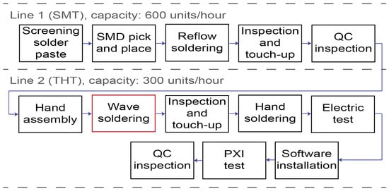
Motion sensor PCBs represent a high-volume product line for the facility, with an annual output of approximately 1,000,000 units distributed across two distinct production lines (baseline layout mapped in Figure 2). The primary objective of this project was to implement PiP technology to eliminate the wave soldering stage, which was previously dedicated solely to assembling the positive and negative battery terminals. To preserve established product integrity, two strict operational constraints were defined: both the solder paste printing parameters for existing SMDs and the pre-established reflow oven thermal profile had to remain unaltered. Consequently, the Critical to Quality (CTQ) metrics were defined around the reduction in operational expenses (lead-free solder alloy, flux, electrical consumption, and stencil fabrication) and the synchronization of production throughput.
Figure 2.
Baseline process map for PCB assembly prior to wave soldering elimination, detailing throughput capacities for surface-mount technology (SMT) and through-hole technology (THT) lines.
2.2. Measurement Phase
During this phase, baseline consumption, manual assembly cycle times, and component thermal resistance were quantified. Consumable expenditures for wave soldering were monitored over a 12-month period, establishing a baseline cost of USD 71,180 (comprising lead-free solder bars, flux, and energy), detailed in Table 1, plus an additional USD 3688 for wave solder pallet fabrication. Furthermore, the critical quality characteristic for the PTH assembly was defined as the barrel fill ratio of the battery terminals. In accordance with IPC-A-610 Class 2 acceptance criteria [18], the lower specification limit (LSL) was firmly set at 75%. Finally, the thermal durability of the terminals was verified via the manufacturer’s Material Safety Data Sheet (MSDS), confirming a fusion temperature of 870 °C, which provides a robust safety margin against the 270 °C peak reflow temperature.
Table 1.
Baseline monthly expenditure for wave soldering consumables (solder, flux, and electrical power) over a 12-month period prior to PiP integration.
2.3. Analysis Phase
Data analysis revealed a severe throughput mismatch between the two production layouts: Line 1 (SMT) operated at a capacity of 600 units/h, while Line 2 (THT and wave soldering) was restricted to 300 units/h, creating a significant logistical bottleneck. By eliminating the wave soldering process, the baseline expenditure of USD 74,868 (consumables and stencils) for 982,456 PCBs translates directly into potential operational savings. Regarding human resource allocation, relocating the two operators responsible for terminal insertion from Line 2 directly to Line 1 (pre-reflow) ensures complete line synchronization. This integration allowed for the total elimination of Line 2 without introducing new bottlenecks in Line 1. Thermally, the substantial delta between the terminal fusion temperature (870 °C) and the peak reflow temperature (270 °C) confirmed the thermodynamic viability of consolidating the assembly into a single heat cycle.
2.4. Improvement Phase
At Line 1, SMT technology and reflow soldering are utilized for component mounting. To solder the positive and negative terminals on this line, it is necessary to achieve the ideal joint features of pin-through-hole (PTH) technology, i.e., a 100% filled barrel and a proper fillet formed on the terminals. To achieve this, it is essential to determine the required solder volume (), which is proportional to the stencil hole dimensions.
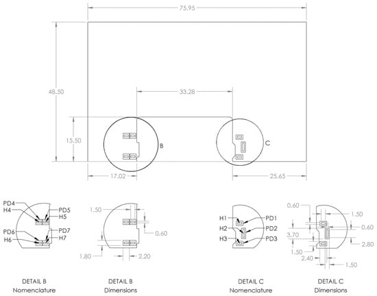
The stencil hole dimensions are calculated based on the hole, pin, and pad dimensions. To accurately determine the required solder volume, a detailed spatial analysis of the components was conducted. Figure 3 presents the CAD layout of the PCB (designed using SolidWorks 2025, Dassault Systèmes, Vélizy-Villacoublay, France), specifically detailing the geometrical configuration and assigned numbering system for the positive and negative terminals (H1 to H7, P1 to P7, and PD1 to PD7). The specific physical dimensions extracted from this technical drawing are compiled in Table 2.
Figure 3.
CAD layout of the PCB detailing the geometrical configuration, dimensions, and nomenclature of the positive and negative terminal footprints. Dimensions are in millimeters and correspond to the volumetric parameters detailed in Table 2.
Table 2.
Geometrical dimensions (length, width, and depth in millimeters) and calculated volumes for the through-holes (H1–H7), pin terminals (P1–P7), and surface pads (PD1–PD7).
Following the methodology established by Phil Zarrow and validated by Krammer et al. [19,20], the required printing solder volume () to ensure complete joint saturation is calculated using the following equation:
where represents the total solder volume required to fill the through-hole, and is the physical volume occupied by the pin terminal. These terms are multiplied by an expansion factor of two to compensate for the volumetric shrinkage (approximately 50%) that solder paste undergoes during the reflow process.
Subsequently, to calculate the precise stencil aperture dimensions, the required printed area () is defined as follows:
where represents the standard stencil thickness (selected as 0.127 mm), and 0.80 serves as an empirical adjustment factor optimized for single fillet formation. Finally, the length and width of each stencil aperture were derived by applying the length-to-width ratio of each corresponding pad (RLApad).
The resulting target values for length and width for each stencil aperture, along with the foundational metrics used for the calculation, are presented in Table 3.
Table 3.
Calculated volumetric requirements and stencil aperture dimensions for PiP implementation, including required solder volume (), printing area (), and pad length-to-width ratio (RLApad).
Based on these mathematical results, the total required solder volume for printing each PCB was established as 8.88 mm3.
2.5. Control Phase
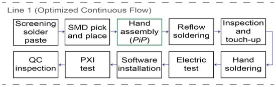
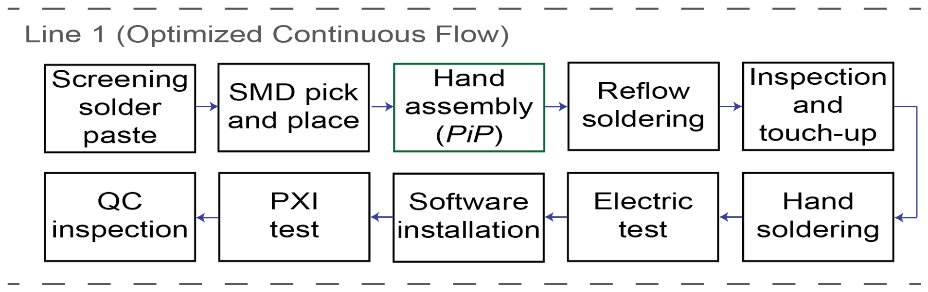
To institutionalize the optimized continuous-flow process, the new sequence, methods, materials, labor allocations, and tools were standardized through updated Standard Operating Sheets (SOSs) [21]. Concurrently, the electronic routing registers controlled by the facility’s Business Planning and Control System (BPCS)—mandatory for compliance in automotive and industrial PCB manufacturing—were systematically revised. These administrative controls ensure stringent adherence to the new PiP protocol, preventing regression to the legacy wave soldering process and permanently securing the operational gains. The resulting optimized continuous-flow process map is illustrated in Figure 4.
Figure 4.
Optimized process map for PCB assembly after PiP implementation, demonstrating continuous flow integration.
3. Results
By implementing PiP technology, the wave soldering process was eliminated from the wireless sensor PCB assembly line. As a direct result, all expenses associated with soldering bars, flux, specialized wave stencils, and targeted electrical energy consumption were eradicated. Furthermore, the wave soldering equipment was physically removed from the production floor; this high-value capital equipment has since been repurposed to manufacture a new product line for the company, avoiding significant secondary investment.
The transition to PiP technology introduced a minor variable expenditure related to the increased paste solder usage for each PCB, quantified at USD 0.00225871 per unit. This was calculated by multiplying the added paste volume per PCB (8.88 mm3) by the volumetric paste solder cost (1 mm3 = USD 0.00025436). Table 4 presents a comprehensive comparison of the production costs before and after PiP technology implementation, detailing the monthly cost variations and the net financial savings achieved.
Table 4.
Comparative analysis of monthly PCB assembly costs and total verified annual savings following the integration of PiP technology.
As demonstrated by the consolidated data in Table 4, the average PCB assembly cost decreased by 97%, culminating in total verified annual savings of USD 92,513. It is important to note that ‘Before’ costs represent empirical financial expenditures (actual material and energy billing), which exhibit natural month-to-month fluctuations due to varying scrap rates, line stops, and process inefficiencies inherent to the legacy wave soldering process.
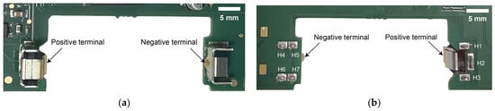
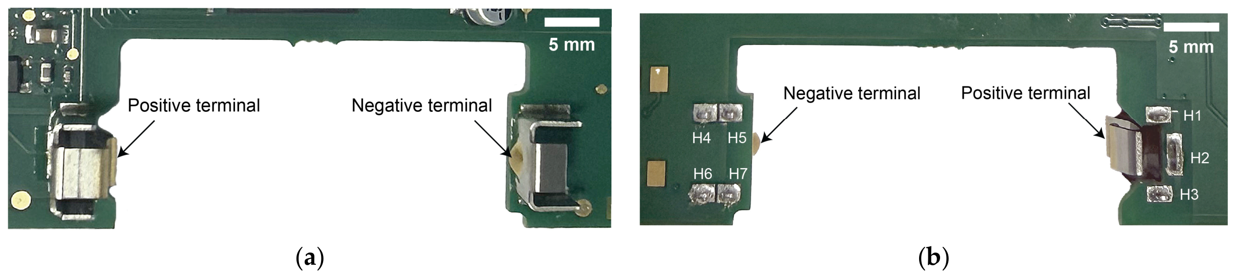
An additional, yet critical, benefit realized from this technological transition was the structural optimization of the PTH assembly. The micro-photographic analysis of the negative and positive terminals validates the metallurgical success of the PiP process consolidation. Figure 5 presents a composite visual validation. Figure 5a shows the top-side insertion of the pins into the PTH. Figure 5b provides a magnified posterior view of the solder joints after reflow. As visually evidenced, robust external solder fillets were formed on the solder side, demonstrating optimal wetting and successful joint consolidation without visible surface voids or bridge defects, adhering to the surface acceptability criteria of IPC-A-610 Class 2 for wetting. The product engineering department corroborated these visual findings by subjecting the assemblies to rigorous soak testing and functional electrical analyses, confirming uncompromised mechanical robustness and electrical continuity.
Figure 5.
Visual validation of the PiP solder joints: (a) top–down view of the consolidated motion sensor PCB; (b) magnified posterior view showing robust solder fillet formation and wetting on the battery terminal pins after reflowing.
Operationally, the manufacturing line now runs in a continuous flow from the initial print to the final stage. This continuous-flow paradigm successfully eliminated work-in-progress (WIP) floor inventory valued at USD 44,025. Concurrently, it eliminated 4.2 km per day of internal material transportation (avoiding a logistics cycle of 105 m traversed 40 times per day). Total operational overhead was further minimized by the total elimination of a legacy touch-up workstation and two redundant quality inspections, as can be observed by comparing the original process map (Figure 2) with the optimized flow (Figure 4) [22].
4. Discussion
The transition to PiP technology facilitated a continuous-flow manufacturing model, successfully correcting the substantial throughput mismatch between SMT and THT assembly stages [5,6,21]. From a material science perspective, consolidating the process into a single heat cycle delivers significant metallurgical advantages: it minimizes the excessive growth of intermetallic compounds (IMCs) and mitigates the risk of thermal degradation in adjacent SMD components, which typically occurs during consecutive reflow and wave thermal cycles [6,7,9]. The environmental co-benefits of this implementation represent a substantive contribution to Green Manufacturing objectives. Wave soldering machines are historically among the most energy-intensive systems in electronics’ assembly, consuming an average of 15–20 kWh [3,5]. Based on the facility’s documented operational schedule of 8 h per day and 250 working days per year, eliminating the wave soldering process reduced electrical consumption by an estimated 30,000–40,000 kWh annually. Applying the carbon intensity factor for Mexico’s national electrical grid (0.444 kg CO2/kWh, as reported by SEMARNAT), this translates directly to a reduction of 13.32–17.76 metric tons of CO2 equivalent per year [23]. Beyond energy savings, wave soldering processes inherently generate hazardous alloy dross due to the oxidation of the molten solder bath, typically at a rate of 3–5% of the total mass consumed. Eliminating this process prevents the generation of approximately 35–60 kg of SAC305 dross per year (calculated based on a 3–5% oxidation rate of the 1190 kg of solder consumed annually), which would otherwise require specialized hazardous material disposal procedures under Mexican environmental regulation NOM-052-SEMARNAT-2005 [24]. Additionally, the liquid flux required for wave operations is a major source of volatile organic compound (VOC) emissions; eliminating the flux stream further reduces the facility’s atmospheric impact. These comprehensive outcomes align tightly with the Lean-to-Green framework, which advocates for the integration of quantifiable environmental sustainability indicators alongside financial performance metrics within the DMAIC framework, ensuring that ecological accountability is fully institutionalized.
5. Conclusions
The implementation of Pin-in-Paste (PiP) technology via a structured Six Sigma DMAIC framework successfully optimized a high-volume PCB assembly line by eliminating the wave soldering process. This transition was executed without altering the established solder paste printing parameters for SMD components or the pre-set reflow oven thermal profile, thereby ensuring strict compliance with IPC-A-610 Class 2 standards. By subjecting the assemblies to a single heat cycle, the added thermal stress on sensitive surface-mount devices was eliminated. In the highly competitive global electronics’ manufacturing market, the operational and financial benefits realized in this study are highly substantial: an annual operational soldering cost reduction of 97%, yielding USD 92,513 in direct savings, a floor inventory (WIP) reduction of USD 44,025, and the elimination of 4.2 km per day of non-value-adding material transport. Furthermore, the project minimized personnel safety risks associated with batch transfer and provided clear Green Manufacturing advantages, reducing greenhouse gas emissions by up to 17.76 metric tons of CO2 equivalent annually while eliminating hazardous dross and VOC emissions. This study provides a validated and scalable framework for facilities seeking to achieve concurrent economic and environmental operational excellence.
Although the PiP methodology successfully consolidated the thermal cycle and eliminated wave soldering inefficiencies in this specific case study, certain limitations must be acknowledged. Future research should focus on long-term thermo-mechanical reliability testing—such as subjecting the PiP joints to accelerated thermal cycling and vibration tests—to fully understand the microstructural evolution of the intermetallic compound (IMC) layer over extended operational lifespans. From an operational automation perspective, future improvements will evaluate transitioning positive and negative terminal packaging to tape-and-reel feeding. This would enable automated SMT pick-and-place insertion, completely eliminating residual manual assembly from the optimized line and advancing toward fully automated continuous flow. Furthermore, while validated in a high-volume sensor manufacturing context, this Lean-to-Green framework offers a scalable blueprint that can be generalized and adapted for higher-complexity assemblies in the automotive and telecommunications sectors, where stringent joint reliability and environmental sustainability are equally critical imperatives.
Author Contributions
Conceptualization, C.J.-V. and D.C.-M.; methodology, C.J.-V. and D.C.-M.; validation, B.S.-S. and G.M.-C.; formal analysis, A.V.-M. and D.C.-M.; investigation, C.J.-V.; data curation, A.V.-M., C.J.-V., B.S.-S. and G.M.-C.; writing—original draft preparation, D.C.-M. and C.J.-V.; writing—review and editing, D.C.-M., J.O.D.-R. and M.A.L.-M.; visualization, B.S.-S., G.M.-C. and D.C.-M.; supervision, D.C.-M. All authors have read and agreed to the published version of the manuscript.
Funding
This research received no external funding.
Data Availability Statement
The data presented in this study is available on request from the corresponding author. Full schematic designs and uncropped macroscopic images of the PCB are not publicly available due to strict corporate confidentiality and intellectual property agreements.
Conflicts of Interest
The authors declare no conflicts of interest.
Abbreviations
The following abbreviations are used in this manuscript:
| PCB | Printed Circuit Board |
| SMT | Surface-Mount Technology |
| PiP | Pin-in-Paste (Intrusive Reflow) Technology |
| DMAIC | Define, Measure, Analyze, Improve, and Control |
| PTH | Pin-Through-Hole Technology |
| THT | Through-Hole Technology |
| WIP | Work-In-Process Inventory |
| SMD | Surface-Mount Device |
| SOS | Standard Operating Sheet |
| BPCS | Business Planning and Control System |
| COPQ | Cost of Poor Quality |
| AXI | Automated X-ray Inspection |
| CTE | Coefficient of Thermal Expansion |
| IMC | Intermetallic Compound |
| VOC | Volatile Organic Compound |
| SAC | Sn–Ag–Cu (Lead-free solder alloy) |
| SAC305 | 96.5% Sn, 3.0% Ag, 0.5% Cu alloy composition |
References
- Hammad, M.; Panaousis, M.; Ali, H.; Khan, W.A. Transforming the Electronics Manufacturing Sector. In Smart Manufacturing Blueprint: Navigating Industry 4.0 Across Diverse Sectors; Springer Series in Advanced Manufacturing; Springer: Cham, Switzerland, 2025; pp. 115–163. [Google Scholar]
- Łyczek, M.; Skarka, W. Review of Methods for PCB Panel Depanelization and Methods for Correct Assembly of Electronic Components on PCB Panels. Electronics 2024, 13, 1255. [Google Scholar] [CrossRef] [Scilit]
- Seidel, R.; Kästle, C.; Ockel, M.; Franke, J. Impact of THT-hole dimensioning on manufacturability in selective wave soldering. Microelectron. Reliab. 2022, 137, 114773. [Google Scholar] [CrossRef] [Scilit]
- Benke, M.; Miko, T.; Koncz-Horvath, D.; Varga, D. Rapid fatigue testing of Through Hole Technology solder joints. Mater. Today Commun. 2025, 47, 113003. [Google Scholar] [CrossRef] [Scilit]
- O’Neill, T.; Jelinske, L. Pin in Paste (PIP) Assembly. Reg. Events 2020, 11, reEJIWO18054. [Google Scholar] [CrossRef] [Scilit]
- Al-Ma’aiteh, T.I.; Krammer, O.; Illés, B. Transient Numerical Modelling of the Pin-in-Paste Technology. Appl. Sci. 2021, 11, 4670. [Google Scholar] [CrossRef] [Scilit]
- Bozsóki, I.; Géczy, A.; Illés, B. Overview of Different Approaches in Numerical Modelling of Reflow Soldering Applications. Energies 2023, 16, 5856. [Google Scholar] [CrossRef] [Scilit]
- Sun, Z.; Huang, X.; Wei, B.; Li, Y. SDD-RT-DETR: A Lightweight and Efficient Printed Circuit Board Surface Defect Detection Method Based on an Improved RT-DETR Toward Sustainable Manufacturing. Sustainability 2026, 18, 2518. [Google Scholar] [CrossRef] [Scilit]
- Zhang, S.; Liu, Y.; Zhang, H.; Zhou, M.; Xue, Y.; Zeng, X.; Cao, R.; Chen, P.-H. Effects of Sn-Ag-x layers on the solderability and mechanical properties of Sn-58Bi solder. Weld. Int. 2021, 35, 16–23. [Google Scholar] [CrossRef] [Scilit]
- Martinek, P.; Illés, B.; Codreanu, N.; Krammer, O. Investigating Machine Learning Techniques for Predicting the Process Characteristics of Stencil Printing. Materials 2022, 15, 4734. [Google Scholar] [CrossRef] [Scilit] [PubMed]
- Mittal, A.; Gupta, P.; Kumar, V.; Owad, A.A.; Mahlawat, S.; Singh, S. The performance improvement analysis using Six Sigma DMAIC methodology: A case study on Indian manufacturing company. Heliyon 2023, 9, e14625. [Google Scholar] [CrossRef] [Scilit] [PubMed]
- Daniyan, I.; Adeodu, A.; Mpofu, K.; Maladzhi, R.; Katumba, M.G.K.-K. Application of lean Six Sigma methodology using DMAIC approach for the improvement of bogie assembly process in the railcar industry. Heliyon 2022, 8, e09043. [Google Scholar] [CrossRef] [Scilit] [PubMed]
- Mogatusi, S.; Takalani, T.; Gupta, K. Leveraging Six Sigma DMAIC for Lean Implementation in Mechanical Workshops. Appl. Sci. 2025, 15, 11788. [Google Scholar] [CrossRef] [Scilit]
- Albar, A.M.; Alsharedah, Y.A.; Irfan, O.M.; Shewakh, W.M. Integrating Lean Six Sigma with Sustainability Goals in Saudi Food Processing: A Case Study Using a Quantitative Framework for Measuring Sustainability Contributions and Cultural Enablers. Sustainability 2026, 18, 2202. [Google Scholar] [CrossRef] [Scilit]
- Monday, L.M. Define, Measure, Analyze, Improve, Control (DMAIC) Methodology as a Roadmap in Quality Improvement. Glob. J. Qual. Saf. Healthc. 2022, 5, 44–46. [Google Scholar] [CrossRef] [Scilit] [PubMed]
- Deepak, D.; Farwaha, H.S.; Alqahtani, F.M.; Dwivedi, S.; Singh, R.P.; Singh, P.; Ranjan, N.; Kumar, A. Enhancement in production efficiency using DMAIC methodology of six sigma. Sci. Rep. 2025, 15, 45109. [Google Scholar] [CrossRef] [Scilit] [PubMed]
- Wang, C.-N.; Nguyen, T.-D.; Nguyen, T.-T.T.; Do, N.-H. The performance analysis using Six Sigma DMAIC and integrated MCDM approach: A case study for microlens process in Vietnam. J. Eng. Res. 2025, 13, 538–550. [Google Scholar] [CrossRef] [Scilit]
- IPC. IPC-A-610H: Acceptability of Electronic Assemblies; Association Connecting Electronics Industries: Bannockburn, IL, USA, 2020. [Google Scholar]
- Zarrow, P. Reflow Soldering of Through-Hole Components. J. Surf. Mt. Technol. 1999, 12, 13–16. [Google Scholar] [CrossRef] [Scilit]
- Krammer, O.; Varga, B.; Dušek, K. New method for determining correction factors for pin-in-paste solder volumes. Solder. Surf. Mt. Technol. 2017, 29, 2–9. [Google Scholar] [CrossRef] [Scilit]
- Amjad, M.H.H.; Shovon, M.S.S.; Begum, M.; Hasan, A.S.M.M. Analyzing Lean Six Sigma Practices in Engineering Project Management: A Comparative Analysis. Am. J. Technol. Adv. 2025, 2, 157–169. [Google Scholar] [CrossRef]
- Wang, C.-N.; Vo, T.T.B.C.; Le, D.-S.; Chung, Y.-C. Optimizing Production Line Efficiency via DMAIC, VSM and FMEA: A Case Study of an Electronics Manufacturing Services Company. Eng. Manag. J. 2025, 1–19. [Google Scholar] [CrossRef] [Scilit]
- SEMARNAT. Factor de Emisión del Sistema Eléctrico Nacional. Available online: https://www.gob.mx/cms/uploads/attachment/file/981194/aviso_fesen_2024.pdf (accessed on 17 June 2026).
- SEMARNAT. Norma Oficial Mexicana NOM-052-SEMARNAT-2005. Available online: https://www.dof.gob.mx/normasOficiales/1055/SEMARNA/SEMARNA.htm (accessed on 17 June 2026).



Disclaimer/Publisher’s Note: The statements, opinions and data contained in all publications are solely those of the individual author(s) and contributor(s) and not of MDPI and/or the editor(s). MDPI and/or the editor(s) disclaim responsibility for any injury to people or property resulting from any ideas, methods, instructions or products referred to in the content. |
© 2026 by the authors. Licensee MDPI, Basel, Switzerland. This article is an open access article distributed under the terms and conditions of the Creative Commons Attribution (CC BY) license.