


Abstract
The Linear Equivalence Signature Scheme (LESS) is a code-based post-quantum candidate in the National Institute of Standards and Technology’s (NIST) standardization process for additional digital signatures. In this paper, we present an area-efficient FPGA accelerator for the Reduced Row Echelon Form (RREF) kernel of LESS, designed for embedded RISC-V SoCs where resource overhead is the primary constraint. Our architecture targets the scheme’s primary computational bottleneck: the linear-algebra core responsible for RREF processing. By implementing an optimized pivot-reuse workflow, our design significantly reduces redundant row-reduction operations across related computations. The accelerator features a matrix-oriented execution engine paired with a streaming control interface to minimize synchronization overhead. Implementation on a Xilinx Artix-7 FPGA shows that despite its compact footprint, the accelerator achieves up to 21× speedup over the embedded software RREF baseline. By prioritizing a minimalist footprint, our design requires only 1.38 to 8.7 KeSlice, depending on the targeted security level. By covering all LESS security levels and providing comparisons with existing post-quantum cryptographic hardware, this work establishes a performance baseline for a signature scheme that has remained largely unexplored in the hardware domain.
1. Introduction
Modern cryptography is a fundamental component of secure digital systems, enabling confidential communication, authentication, and data integrity. The security of currently deployed public-key schemes, such as RSA, Diffie–Hellman, and Elliptic-Curve Cryptography (ECC), relies on the computational hardness of problems like integer factorization and discrete logarithms. However, the advent of quantum computing challenges this assumption. Specifically, Shor’s algorithm [1] demonstrates that these problems can be solved efficiently on a sufficiently powerful quantum computer, threatening the security of existing public-key infrastructures. In response to this systemic vulnerability, the National Institute of Standards and Technology (NIST) initiated a comprehensive standardization process to identify and vet quantum-resistant primitives [2].
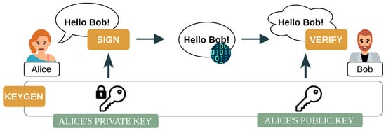
This transition to Post-Quantum Cryptography (PQC) focuses on two primary pillars of secure communication: Key Encapsulation Mechanisms (KEMs), which replace traditional Public-Key Encryption for secure key exchange, and Digital Signature (DS) schemes, which ensure the authenticity and integrity of data. While the initial NIST standardization process successfully identified a first set of quantum-resistant schemes, the selected digital signatures were predominantly based on structured lattices and hash functions. To ensure a diversified portfolio of security assumptions and to explore algorithms with different performance trade-offs, such as smaller signature sizes or faster verification, NIST launched a call for additional digital signature schemes, commonly referred to as the PQC “on-ramp”. In October 2024 (https://csrc.nist.gov/News/2024/pqc-digital-signature-second-round-announcement—accessed on 16 April 2026), NIST announced the 14 candidates selected to advance to the second round of this on-ramp process, highlighting the ongoing evolution of the PQC landscape. Fundamentally, these candidates all implement a standard digital signature scheme, which provides non-repudiation in a public-key setting. As illustrated in Figure 1, which depicts a standard communication scenario between a sender (Alice) and a receiver (Bob), a digital signature scheme typically consists of three core algorithms:
Figure 1.
Digital Signature Scheme.
- Key Generation (KEYGEN): The sender, Alice, computes a mathematically linked public and private key pair (). She securely stores her private key and openly distributes her public key.
- Signing (SIGN): To authenticate a given message (M), Alice uses her private key () to generate a unique digital signature () bound to that specific message.
- Verification (VERIFY): Upon receiving the message and the signature, the receiver, Bob (or any other entity), uses Alice’s public key () to check the validity of against M. The algorithm outputs a Boolean “accept” or “reject” signal, ensuring the message was genuinely signed by Alice and has not been altered in transit.
Despite their robust security guarantees, these post-quantum algorithms, including the new on-ramp candidates, introduce significant computational overhead compared to their classical counterparts. They frequently rely on complex mathematical foundations involving high-degree polynomial arithmetic, large matrix operations, or intensive hashing sequences. This creates a severe performance bottleneck, particularly for embedded systems and Internet-of-Things (IoT) devices constrained by limited power budgets and low clock frequencies. Consequently, hardware acceleration has emerged as a vital necessity to make PQC viable in real-time, resource-constrained environments. In the landscape of hardware acceleration, various loosely coupled coprocessors have already been proposed. However, the vast majority of these works target the already standardized algorithms, focusing on specific primitives like lattice-based schemes or hash-based signatures [3,4,5,6,7,8,9]. In contrast, research exploring dedicated hardware architectures for new candidates is only just beginning to emerge [10,11,12,13,14,15].
Addressing the need for efficient implementations of the newer candidates, this work proposes a hardware accelerator for one of the on-ramp algorithms: LESS, the Linear Equivalence Signature Scheme [16,17]. LESS is a code-based signature scheme whose execution time, as identified through software profiling, is overwhelmingly dominated by a single computational kernel: the Reduced Row Echelon Form (RREF) computation. Although LESS did not advance to the subsequent stage of NIST’s additional digital signature standardization process [18], it remains one of the few code-based signature schemes that reached the later phases of the evaluation. Furthermore, rather than implementing the entire signature scheme in hardware, we adopt a modular approach that accelerates only the RREF computations and focuses on efficient hardware/software co-design for linear-algebra kernels, making this work applicable to a broader class of code-based and matrix-oriented post-quantum cryptographic constructions. The proposed loosely coupled accelerator is integrated within a RISC-V-based embedded platform using X-HEEP [19], a lightweight microcontroller-class system designed for the research and rapid prototyping of hardware extensions. This design choice maximizes hardware efficiency while preserving the flexibility of the general-purpose processor to handle the remaining protocol logic. The main contributions of this work can be summarized as follows:
- Profiling of the LESS digital signature scheme on an embedded RISC-V software flow, identifying the RREF computation as the dominant kernel to be accelerated;
- Design of an area-centric FPGA accelerator for the RREF kernel of LESS, targeting embedded deployments where logic footprint, BRAM occupation, and power consumption are primary design constraints;
- Integration of the accelerator as a loosely coupled memory-mapped peripheral in a RISC-V SoC, with DMA-based matrix transfers and interrupt-driven synchronization to account for realistic software/hardware communication overhead;
- Evaluation of the proposed design across the LESS security levels on a unified Xilinx Artix-7 implementation flow, reporting kernel-level acceleration, full SIGN/VERIFY impact, resource occupation, power estimates, and comparison with existing FPGA implementations.
Organization. The rest of the paper is organized as follows: Section 2 describes the theoretical background of LESS, its algorithmic structure, and the profiling conducted to identify its main bottlenecks when executing on a 32-bit System on Chip (SoC). Section 3 presents the architectural details of the proposed design, and Section 4 details its integration into the target platform. Finally, Section 5 evaluates the architecture in terms of performance, resource utilization, and scalability across different security levels, while Section 6 discusses future developments of the works. Finally, Section 7 presents the conclusions of this work.
2. Background
This section outlines the motivation of this work and the essential background of the LESS signature scheme [16,17]. It presents the underlying algebraic principles, details the construction of the scheme, and describes its core algorithms, with a focus on the computational structures that drive the execution cost.
2.1. Application Value and Motivation for Hardware Acceleration
Beyond computational latency, one of the principal challenges limiting the adoption of post-quantum digital signatures in embedded platforms is their hardware cost. Existing hardware accelerators for PQC signatures frequently prioritize throughput through extensive parallelization, resulting in implementations that require tens of thousands of LUTs and substantial on-chip memory resources. While such architectures are appropriate for servers, gateways, and high-end FPGA platforms, they are often incompatible with resource-constrained environments such as IoT nodes, edge devices, secure sensors, and portable systems, where only a small fraction of the available silicon area can be dedicated to cryptographic functions. Consequently, minimizing hardware footprint is not merely an implementation optimization, but a fundamental requirement for practical deployment.
As the transition to Post-Quantum Cryptography (PQC) accelerates, ensuring cryptographic diversity has become paramount to avoid relying on a single family of mathematical hardness assumptions. Within this landscape, code-based cryptography is recognized for its highly conservative security guarantees [17]. LESS stands out as an intriguing candidate because its security is not based on traditional syndrome decoding, but entirely on the Linear Equivalence Problem (LEP). This distinct algebraic foundation provides a crucial structural alternative should unexpected vulnerabilities be discovered in the ubiquitous lattice-based schemes. Recently, LESS has evolved to incorporate canonical forms, a technique that dramatically reduces its signature sizes down to 1– KB for NIST Category 1 security levels. This exceptional compactness makes LESS highly attractive for bandwidth-constrained applications, such as automotive networks, secure boot mechanisms, and distributed Internet-of-Things (IoT) ecosystems where transmitting large cryptographic payloads is prohibitive. Furthermore, when compared to other Zero-Knowledge-based submissions, LESS positions itself as a remarkably strong candidate by offering some of the smallest signature sizes available.
However, this reduction in signature size introduces a fundamental trade-off: computing these canonical forms and the associated Reduced-Row Echelon Forms (RREF) adds significant computational overhead. In software implementations, these dense matrix transformations represent a severe performance bottleneck, consuming the vast majority of the execution time during both signing and verification.
Therefore, while the mathematical elegance and small signature footprint of LESS present clear application advantages, its software latency remains a limiting factor for real-time systems. Hardware acceleration is not merely an optimization, but a necessary enabler. By designing dedicated FPGA architectures to offload these heavy linear algebra operations, we can bridge the gap between LESS’s compact communication requirements and the high-throughput, low-latency execution demanded by modern resource-restricted embedded systems.
2.2. LESS: Signatures from Linear Code Equivalence
LESS (Linear Equivalence Signature Scheme) is a post-quantum cryptographic protocol whose security relies on the hardness of identifying linear equivalences between codes, distinguishing it from traditional decoding-based assumptions. At its core, the scheme publishes one or more transformed versions of a secret linear code, generated via group actions. To prove knowledge of the secret isometry linking these public instances, the signer executes a -protocol, which is made non-interactive using the Fiat–Shamir transform [20].
Notation and preliminaries. Let be the finite field of order q (in the standard LESS parameter sets, q is a small prime, often ). For integers , a matrix defines a linear code through its row space:
Two generator matrices related by left multiplication with an invertible matrix (the group of invertible matrices over ) define the same code, as this operation corresponds to a change of basis in the message space. A monomial matrix has exactly one non-zero entry per row and per column; equivalently, with a permutation matrix P and an invertible diagonal matrix D. Right-multiplication by Q permutes and rescales coordinates, hence maps a code to a monomially equivalent one:
The Linear Equivalence Problem (LEP) asks, given , whether there exist and a monomial Q such that:
In LESS, security relies on the hardness of recovering such a hidden monomial transformation, under appropriate parameter choices and input distributions.
To compare public objects and commitments efficiently inside protocol transcripts, LESS uses a canonical representation based on Reduced Row Echelon Form (RREF). Since RREF depends only on the row space, the unknown left factor S in (1) is eliminated:
As a result, after canonicalization, only the effect of the monomial right action remains. During verification, LESS further canonicalizes the non-pivot part (typically denoted V in a systematic form ). Each non-pivot column is normalized (e.g., via lexicographic minimization under column scaling), and the columns are then sorted. This ensures that equivalent representations do not affect the input to the Fiat–Shamir hash function.
LESS parameters. LESS is instantiated with code parameters and protocol parameters , where t denotes the number of (simulated) -protocol rounds, is the fixed Hamming weight of the challenge vector (i.e., the number of non-zero challenges among the t rounds), and s is the number of public/secret challenge slots. Table 1 summarizes the parameter values for the different LESS variants across the three NIST security levels. Increasing t reduces the soundness error. The fixed-weight challenge structure enables compact transcripts, while larger values of s increase the public key size but allow for shorter signatures.
Table 1.
LESS parameter sets and public key/signature sizes.
2.3. LESS Algorithm
Below, the algorithms are written at the scheme level. Concrete byte layouts follow the LESS NIST API and the repository structure [21].
LESS.KeyGen. Key generation (Algorithm 1) samples a base matrix from a public seed and derives secret monomial inverses from additional seeds. It then publishes the corresponding RREF-compressed matrices. The public key consists of , used to reconstruct , together with the compressed RREF representations of each .
The secret key contains the seeds used to generate the monomial inverses ; the identity slot is implicit and therefore not stored. It is important to note that while key generation requires computing RREFs to derive these public representations, it is a one-time setup operation. Consequently, it is executed entirely in software on the host CPU and is not offloaded to the hardware accelerator.
| Algorithm 1 LESS.KeyGen |
|
LESS.Sign. LESS signatures (Algorithm 2) are generated via a Fiat–Shamir transformation of a multi-round -protocol with fixed-weight challenges. The signer first produces t commitments by sampling ephemeral monomials and computing the corresponding canonical commitment encodings . A digest d is then computed by hashing all commitments together with the message and a salt. This digest is expanded into a challenge vector of fixed Hamming weight . To compress the transcript, only the responses corresponding to non-zero challenges are included in the signature. The remaining randomness is recovered by the verifier using a seed-tree construction.
For each non-zero challenge , the response encodes a compressed description of the monomial transformation that maps the public slot to the commitment in round i. In the literature, this response is typically described as an encoding of [22].
| Algorithm 2 LESS.Sign |
|
LESS.Verify. Verification (Algorithm 3) reconstructs all commitments from the signature as follows:
- If , the verifier regenerates from the corresponding seed-tree leaf and recomputes the commitment via .
- If , the verifier decodes the response into a monomial transformation, applies it to the public matrix , and then canonicalizes the result by computing its RREF representation followed by lexicographic minimization and lexicographic sorting of the non-pivot columns.
Finally, the verifier hashes the reconstructed commitments and checks whether the resulting digest matches d.
| Algorithm 3 LESS.Verify |
|
2.4. LESS Profiling
To pinpoint the primary computational bottlenecks and guide the hardware architecture, the LESS reference implementation was profiled using ASIP Designer [23]. The analysis relied on inputs derived from the official Known Answer Tests (KATs) to guarantee deterministic execution and reproducibility across varying security levels.
As detailed in Table 2, the profiling results reveal a heavily skewed computational load. The generator_RREF_pivot_reuse function thoroughly dominates the execution, consuming 87.73% of the total clock cycles during the signing procedure. From a theoretical perspective, the standard sequential RREF transformation of a generator matrix requires an asymptotic time complexity of finite field operations. Concurrently, the total deterministic space complexity needed to store the matrix payload and its tracking structures is bounded by . Conversely, other essential tasks, such as canonical form computation and Keccak-based hashing, contribute only a marginal fraction to the overall latency. The performance of the LESS signing algorithm is hence bottlenecked almost entirely by the RREF kernel, which predominantly arises during the SIGN and VERIFY phases. As a result, any optimization targeting this function directly translates into significant end-to-end performance improvements. Conversely, the remaining components of the algorithm account for only a limited fraction of the total latency. Canonical form computations, while related to the RREF process, involve simpler post-processing steps such as column normalization and sorting, and therefore incur a lower computational cost. Similarly, Keccak-based hashing operations, although essential for security, are efficiently handled and contribute only marginally to the overall cycle count.
Table 2.
Computational workload distribution of the LESS signing procedure.
Consequently, dedicating hardware acceleration to the RREF function offers the highest potential for minimizing total execution time.
3. Hardware Implementation
The proposed hardware design for the RREF computation is implemented as an autonomous, loosely coupled compute engine. By offloading the row-reduction procedure to dedicated hardware, the system achieves a clear separation of concerns between software orchestration and hardware execution. The host processor is solely responsible for initial configuration, defining matrix dimensions and security parameters, and pushing the input dataset to the accelerator. Once triggered, the hardware independently manages all algorithmic phases, including pivot selection, row scaling, and elimination.
This decoupled execution model frees the host from cycle-level synchronization while allowing the accelerator to exploit internal parallelism and local memory for deterministic, high-throughput operation.
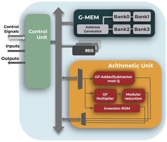
Architecturally, the accelerator mirrors the reference software implementation (https://www.less-project.com/—accessed on 12 December 2025), mapping the algorithmic phases onto a state-machine-driven datapath optimized for parallel execution. As illustrated in Figure 2, the core internal modules comprise:
Figure 2.
Top-Levelarchitecture of the RREF Accelerator.
- Control Unit: The centralized FSM that acts as the brain of the accelerator, dynamically sequencing operations and managing the activation and reset of all other internal modules.
- G-MEM: On-chip BRAM storage for the generator matrix. This memory-centric approach was adopted after early full-register prototypes exceeded available LUT and register limits, even for the smallest parameter sets.
- Arithmetic Unit: A parallelized suite of operators dedicated to finite-field addition, subtraction, multiplication, and multiplicative inversion over .
- REG: A generic block representing the internal storage elements. This encompasses both the dedicated state registers used to track historical and current pivot positions (the was/is pivot registers), as well as the temporary pipeline buffers utilized for intermediate data storage during multi-cycle row manipulations.
At the interface level, communication between the accelerator and the host system is abstracted into three broad categories. The external connections routed to the Control Unit are generically grouped as inputs, outputs, and control signals. The inputs form the data channels carrying the initial generator matrix, historical pivot maps, and configuration parameters into the system. The outputs handle the return streams, passing the fully reduced matrix and updated pivot maps back to the host. Finally, the control signals encompass all the single-bit handshakes, start triggers, read/valid markers, and status flags required to coordinate the data flow and algorithmic phases without exposing the cycle-level complexity to the software layer.
- Control Unit and Execution Model
The Control Unit (CU) sequences the execution of the RREF algorithm. Rather than relying on a deeply pipelined dataflow architecture, the design uses a centralized Finite State Machine (FSM) that operates on the matrix stored in the on-chip BRAM (G-MEM). Operations are executed using a word-parallel memory access pattern (processing four 8-bit finite-field elements per cycle). The FSM abstracts the complexity of multi-cycle memory operations (read–modify–write sequences) and orchestrates the computation through four primary algorithmic phases:
- Preprocessing: before performing standard elimination, the accelerator leverages previously identified pivot information to pre-align the matrix structure. It scans the set of known pivot columns and applies the required row swaps to restore non-zero entries to their canonical diagonal positions. Restricting this procedure to historical pivot columns bounds the execution time and avoids unnecessary searches.
- Pivot Discovery: starting from the active diagonal position, the CU searches downwards across the rows of the current column to locate a non-zero element. If a valid pivot is found in a subsequent row, the unit executes a word-parallel row swap to bring it to the diagonal. To optimize performance, this phase conditionally reuses historical pivot maps to bypass redundant searches when valid structural knowledge already exists.
- Row Normalization: once a pivot is aligned, the row must be scaled so that the pivot element becomes exactly 1. The CU fetches the pivot element, computes its multiplicative inverse over , and sequentially applies this scaling factor to the entire pivot row. Exploiting the 32-bit datapath, four elements are scaled and written back to memory simultaneously.
- Column Elimination: the normalized pivot row is used as a reference to zero-out the pivot column entries in all other rows. The CU iterates through every non-pivot row, fetches the element in the pivot column to use as an elimination multiplier, and applies the standard Gaussian elimination rule. Entire rows are updated using word-parallel finite-field multiply-and-accumulate operations until the pivot column is fully cleared.
Upon the successful iteration of these four phases across all matrix columns, the engine concludes the reduction process. The finalized matrix, along with the updated pivot tracking maps, is then explicitly streamed back to the host to complete the hardware–software synchronization.
- G-MEM
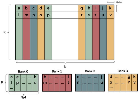
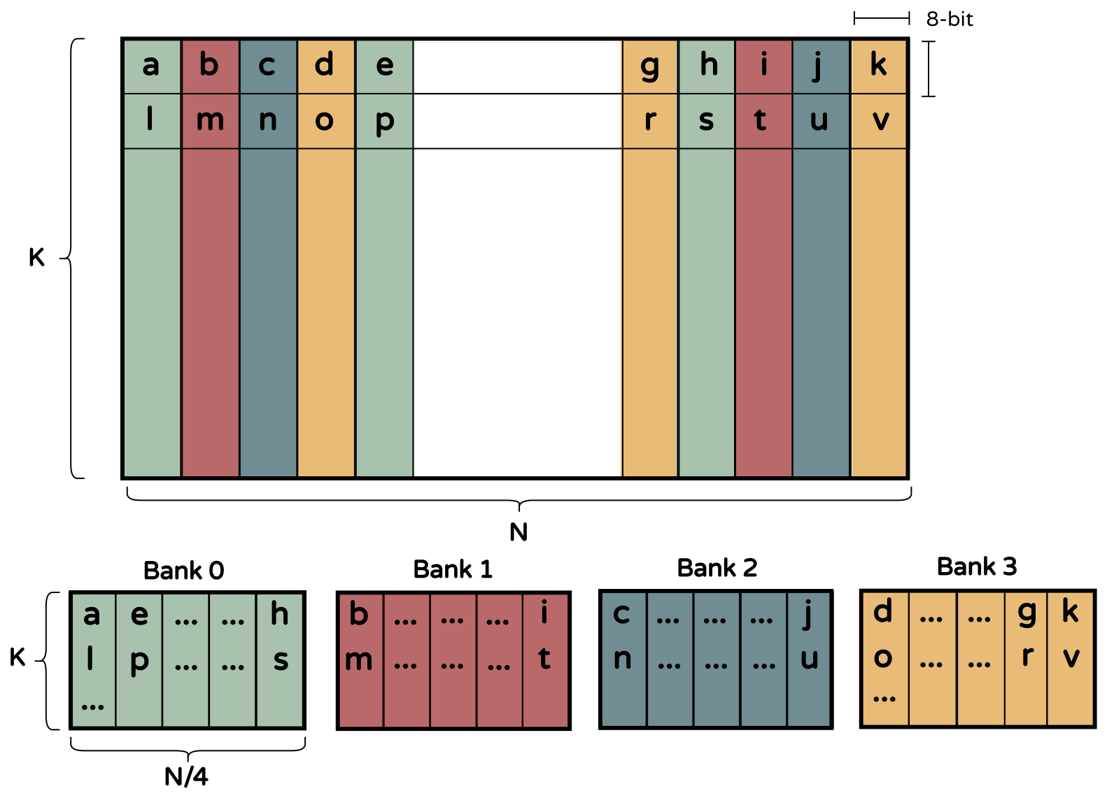
The Generator Matrix Memory (G-MEM in Figure 2) serves as the primary on-chip storage for the matrix G, utilizing synchronous FPGA Block RAM (BRAM) resources to balance storage capacity with access speed. Given that the RREF algorithm is inherently memory-bound due to frequent row-based read–modify–write operations, this subsystem is engineered to sustain high throughput while minimizing the utilization of LUT and flip-flop resources. Logically, the matrix is organized in row-major order, where each field element is represented by a single 8-bit byte. This allows the Control Unit (CU) to calculate the specific linear address for any element at position using the formula . Physically, the memory is partitioned into four parallel 8-bit banks (Bank 0 to Bank 3), an interleaved organization detailed in Figure 3.
Figure 3.
Interleaved organization of the synchronous memory storing matrix G. The memory stores exactly GELEMS = K × N field elements. Each square block represents a single 8-bit field element.
This banking scheme enables the accelerator to access a full 32-bit word, containing four consecutive field elements, in a single clock cycle by concatenating the outputs: . To maintain efficiency during non-aligned operations, the system employs an Address Alignment and Rotation block. When a request is made, the 32-bit address is decomposed into a word index () and a byte offset (). A rotation network or barrel shifter then realigns the retrieved bytes based on the registered offset, ensuring that unaligned reads do not incur performance penalties or require multiple memory cycles. Similarly, the write path leverages a 4-bit byte-enable signal () to update specific field elements within a word, facilitating precise row modifications without needing a pre-fetch read cycle. The entire memory architecture is optimized for a deterministic 1-cycle latency for both reads and writes. This predictability is a critical architectural feature, as it allows the CU to schedule finite-field arithmetic operations via the mem_phase micro-sequencer with cycle-accurate precision. This ensures that the parallel lanes of the Arithmetic Unit are fed with fresh data exactly when needed, maximizing the overall throughput of the reduction process.
- Arithmetic Unit
The mathematical operations required by the RREF algorithm over are executed by a low-overhead, purely combinational Arithmetic Unit (AU). To maintain architectural modularity, these finite-field primitives are implemented as synthesizable functions within a shared package and are directly invoked by the CU during matrix transformations. To maximize the efficiency of the 32-bit memory subsystem, the AU is designed with a four-lane parallel structure. This organization allows the processing of four field elements in a single clock cycle, matching the word-width of the generator matrix memory and ensuring that arithmetic execution does not become a bottleneck for the memory-bound reduction process.
Field Representation and Modular Reduction. The choice of the finite field with significantly simplifies the hardware implementation. Since 127 is a Mersenne prime (), modular reduction can be performed without the need for complex and resource-intensive division circuitry. The reduction logic exploits the property that . Consequently, any 14-bit product x resulting from the multiplication of two field elements can be reduced by folding the upper 7 bits onto the lower 7 bits:
In the proposed implementation, matrix elements are stored as 8-bit bytes for alignment with standard memory structures, even though only 7 bits are mathematically significant. Intermediate multiplication results are stored in a 16-bit format to prevent overflow before the reduction stage.
The AU provides three core primitives to the Control Unit:
- Modular Addition/Subtraction: these units handle the row combinations required during the Gaussian elimination phase, ensuring results remain within the range (GF-adder/subtractor mod Q in Figure 2).
- Modular Multiplication: four parallel multipliers execute the scaling and elimination rules (GF Multiplier). As depicted in Figure 2, each lane is followed by a combinational reduction stage (Modular Reduction).
- Multiplicative Inversion: due to the small size of the field, the multiplicative inverse is implemented via a 128-entry Lookup Table (LUT) (Inversion ROM). This provides constant-time latency for the pivot normalization step, avoiding the complexity of the Extended Euclidean Algorithm.
Since the AU is entirely combinational, its operational latency is fully absorbed into the micro-phased execution model of the Control Unit. During the SCALE_ROW_LOOP phase, the AU normalizes the pivot row by broadcasting a single precomputed scaling factor across the four multiplier lanes. In the REDUCE_COL_LOOP phase, the unit performs a parallel multiply-and-subtract operation to eliminate pivot column entries in the target rows. By activating these arithmetic blocks only during specific FSM states, the design minimizes unnecessary switching activity and power consumption.
- REG
The REG block (Figure 2) groups the internal register structures required to support pivot tracking and row-level operations. It provides the temporary storage and state persistence needed to coordinate data movement between the CU, the on-chip memory, and the AU. Pivot information is maintained through two N-bit register vectors, was_pivot and is_pivot, encoding previously known and newly discovered pivot positions, respectively. The was_pivot vector is initialized by the host and enables the reuse of prior structural information during preprocessing and pivot discovery, reducing unnecessary searches. The is_pivot vector is updated during execution and returned at completion. Both are implemented as synchronous register arrays, ensuring single-cycle access with minimal hardware cost. Row operations are supported by a set of temporary registers that buffer matrix data during read–modify–write sequences. Since the matrix is accessed as 32-bit words, these registers store intermediate values while data is fetched from memory, processed by the AU, and written back. In particular, the REG block includes:
- Row buffers: temporary storage for matrix words during swap and elimination operations;
- Scaling registers: holding the pivot inverse used during row normalization;
- Elimination registers: storing the coefficient used to eliminate pivot-column entries in target rows.
A set of index and address registers tracks the current position within the matrix and drives memory addressing, allowing the CU to traverse rows and columns across the different phases of the algorithm. A lightweight micro-phased execution scheme is used to align memory accesses with computation, decomposing each operation into a sequence of tightly scheduled steps that account for the synchronous memory latency.
4. Integration
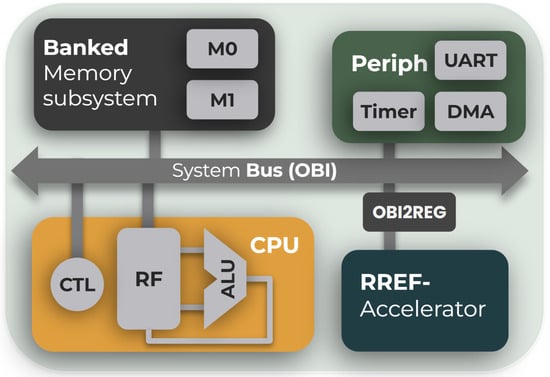
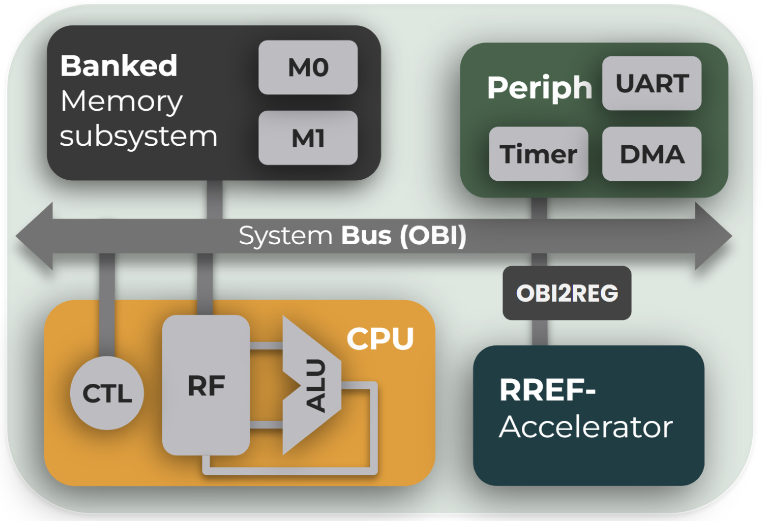
The RREF accelerator is integrated into the X-HEEP (https://github.com/x-heep/x-heep—accessed on 1 July 2025) platform as a loosely coupled memory-mapped peripheral (Figure 4). This modular approach is specifically tailored for resource-constrained environments: by offloading the long, data-intensive RREF transformation to an autonomous core, the system preserves the primary RISC-V processor for high-level protocol logic while minimizing the total silicon footprint.
Figure 4.
Top-Level architecture of the RREF Accelerator integrated into X-HEEP.
To prevent the performance bottlenecks typical of low-power SoCs, the interface strictly bifurcates control and data paths. While control signals and compact metadata (e.g., pivot maps) are managed via lightweight MMIO registers, the dense matrix payload G bypasses the CPU entirely. Instead, bulk data is handled by the system’s DMA controller, ensuring high-throughput streaming directly into the accelerator’s local memory without cycle-stealing from the host.
A lightweight driver abstracts the hardware complexity, providing a consistent execution model for both cycle-accurate simulation and FPGA validation. The driver replaces inefficient polling with an interrupt-driven synchronization scheme utilizing the platform’s PLIC. This allows the CPU to enter a low-power state via the wfi (Wait-For-Interrupt) instruction during hardware execution. The workflow is organized into four deterministic phases:
- Initialization: The driver enables PLIC interrupts and configures initial runtime parameters, such as pivot reuse limits, via Memory-Mapped I/O (MMIO).
- Offloading & Execution: The CPU initiates the DMA transfer for the matrix payload G, while the pivot metadata is packed into 32-bit words and written to MMIO registers. Once the start command is issued, the CPU sleeps until the hardware asserts the completion interrupt.
- Results Retrieval: Upon waking, the driver triggers a reverse DMA transfer to stream the reduced matrix back to main memory. Simultaneously, the CPU retrieves the updated pivot masks directly from the hardware output registers.
- Verification: The driver confirms the successful culmination of all streams and checks the hardware status registers for operational errors before returning control to the higher-level LESS signature protocol.
By keeping control-heavy logic in software and accelerating only the dominant computational kernel, this co-design achieves the high-security guarantees of the LESS scheme within a minimalist hardware footprint, making it ideal for devices where silicon area is at a premium.
5. Results
This section evaluates the proposed RREF accelerator within the LESS software–hardware flow. All hardware measurements are reported on a unified Xilinx Artix-7 target, namely the xc7a100tftg256-2 device. The use of a single implementation target enables a fair comparison between the different LESS security levels and avoids attributing device-dependent effects to architectural properties. The accelerator is described in synthesizable RTL and is integrated as a loosely coupled memory-mapped peripheral. Its architecture does not rely on vendor-specific arithmetic macros and communicates with the host through standard MMIO control registers and DMA-based data transfers. Therefore, the design can be retargeted to other FPGA-based RISC-V SoCs by adapting the memory and interconnect wrappers. However, since timing, routing, BRAM mapping, and power strongly depend on the selected device, the quantitative results reported in this section are intentionally restricted to the Artix-7 flow.
The software baseline is obtained by executing the original RREF software routine within the same embedded RISC-V software flow used to drive the accelerator. The code is compiled for the RV32IM instruction set using the -O2 optimization level. Cycle counts are collected using the platform cycle counter over 100 Known Answer Test vectors and are averaged across the executions. Therefore, the reported software baseline should be interpreted as an embedded RISC-V baseline, not as a comparison against desktop-class CPUs or high-performance processors.
5.1. Performance
To clarify the scope of the measurements, three different performance levels are reported. First, Table 3 isolates a single RREF call and compares the original software implementation with the hardware-accelerated execution. Second, Table 4 reports the complete offload cost, including host-side preparation, DMA matrix upload, MMIO pivot transfer, interrupt-driven synchronization, hardware computation, matrix readback, and final synchronization. Third, Table 5 reports the impact of the accelerator when inserted into the full LESS SIGN and VERIFY flows. This separation prevents the standalone kernel speedup from being confused with the complete system-level speedup.
Table 3.
Original Software vs. Optimized Hardware for a Single RREF Function Call.
Table 4.
Cycle breakdown of the hardware-accelerated RREF execution.
Table 5.
System-level performance: Original vs. Optimized cycles for Sign and Verify.
Table 3 reports the performance of a single RREF computation. The accelerator achieves a speedup of approximately 20–21× with respect to the embedded RISC-V software baseline. This value refers only to the RREF kernel and should not be interpreted as the speedup of the complete LESS signature flow.
The full offload cost is detailed in Table 4. The execution is divided into three phases: Prep, which includes DMA setup, matrix upload, interrupt configuration, and pivot metadata transfer; Compute, which corresponds to the autonomous hardware execution; and Readback, which includes matrix retrieval, pivot-vector readback, and synchronization. The measured overhead remains below 1% for all security levels, showing that DMA-based transfers and interrupt-driven synchronization are sufficient to prevent the RISC-V host interface from dominating the execution time.
When integrated into the full LESS protocol flow, the proposed hardware accelerator provides substantial end-to-end performance gains for both Sign and Verify operations, as detailed in Table 5. Across the evaluated parameter sets, the system-level speedup ranges from to over . The considered parameter sets correspond to the different LESS security levels, each defined by specific matrix dimensions that determine the size of the generator matrix and the overall computational workload.
Although, as highlighted by the profiling results reported in Table 2, the RREF computation remains by far the dominant kernel in the LESS signing and verification flow, the acceleration obtained in Table 5 is lower than the standalone kernel speedup. The total speedup is indeed limited by the non-accelerated portions of the protocol, such as hashing, control flow logic, and data movement. Notably, the overall efficiency gains scale positively with the security level. As matrix dimensions and the number of iterations increase, the RREF kernel becomes a larger fraction of the total execution time, enabling the hardware to achieve a higher return on investment. From a security perspective, the accelerator is designed to exhibit constant-time behavior. Unlike software implementations where branching on non-zero elements can introduce significant timing side-channels, the hardware FSM manages pivot discovery and row elimination through a deterministic sequence of operations. The control flow depends only on the public matrix dimensions and the configuration parameters, rather than the secret values of the field elements. To verify this stability, we analyzed the execution of 100 iterations using different KAT vectors. The results show a negligible cycle-count variance, typically less than 300 cycles, which, for executions lasting millions of cycles, confirms a high degree of temporal determinism in the evaluated cycle counts. However, this observation is not sufficient to claim resistance against power, electromagnetic, or fault attacks, which require a dedicated leakage and fault-injection assessment.
Furthermore, results for the KeyGen phase are not reported in this evaluation. Although the key generation process mathematically computes RREFs to derive the public key matrix slots (as detailed in Algorithm 1), this is a one-time setup procedure typically executed offline by the host processor. The highly repetitive generator_RREF_pivot_reuse workload, which dictates the strict latency constraints of the scheme, occurs exclusively during the Sign and Verify phases. Therefore, the KeyGen phase does not utilize the proposed hardware accelerator.
5.2. Area
The hardware footprint remains exceptionally compact across all synthesized configurations, as summarized in Table 6. In accordance with our primary design requirement of area-efficiency, the architecture maintains a minimalist profile even when scaled to the highest security levels. Specifically, the design requires fewer than 3700 LUTs and 1600 Flip-Flops for Category 5 security, utilizing an order of magnitude less logic than existing high-throughput implementations. This confirms that the substantial system-level speedup is achieved without compromising the feasibility of deployment on resource-constrained edge devices. Table 6 details the post-implementation resource consumption, highlighting the accelerator’s lean integration profile.
Table 6.
Post-implementation hardware resources of the LESS accelerator across security levels.
By deliberately opting for a more serialized, area-optimized execution engine, we ensure that the architecture is integration-limited rather than compute-limited. This design philosophy provides the necessary timing closure slack to allow for seamless porting across different FPGA fabrics, including those with lower performance grades, without sacrificing the core objective of a compact, secure digital signature solution.
5.3. Power
Power consumption measurements for the synthesized accelerator are reported in Table 7. The estimates were obtained after place-and-route on the target FPGA platform and include both static and dynamic contributions. Overall, the proposed architecture maintains a relatively low power footprint across all evaluated security levels. As expected, the dynamic power consumption increases with the matrix dimensions and with the amount of active hardware resources required by larger configurations. In particular, the higher BRAM and DSP utilization of the Level 5 implementation leads to the largest dynamic contribution. Nevertheless, the total power consumption remains below 230 mW even for the most demanding configuration.
Table 7.
Post-implementation power consumption of the LESS accelerator across security levels.
The results further confirm the area-oriented design philosophy adopted throughout this work. Since the architecture relies on a serialized execution model with limited parallel arithmetic units, the switching activity remains comparatively modest despite the substantial performance acceleration achieved at the system level.
5.4. Comparison with Existing FPGA Implementations
Table 8 compares the proposed design with representative FPGA implementations of post-quantum digital-signature accelerators, including CROSS [10], CRYSTALS-Dilithium [24], and the original LESS hardware reported by Beckwith et al. [22]. The comparison is mainly intended to position the proposed architecture in terms of hardware footprint. Absolute latency comparisons are intentionally avoided when prior works do not report compatible cycle counts or implement a different portion of the cryptographic scheme.
Table 8.
Comparison with State-of-the-Art FPGA Implementations (Xilinx Artix-7).
This distinction is particularly important for LESS. The design in [22] implements a high-throughput architecture for the complete scheme, whereas the proposed work accelerates the dominant RREF kernel within a software/hardware RISC-V flow. Consequently, the main conclusion drawn from Table 8 is not that the proposed design is the fastest absolute implementation, but that it occupies a substantially smaller area point in the design space.
The resulting KeSlice values, defined in Equation (2), further highlight the area efficiency of the architecture.
The proposed accelerator reduces the logic footprint by adopting a serialized four-lane datapath and local BRAM-based matrix storage instead of aggressive unrolling. This design choice trades maximum throughput for compactness, enabling LESS acceleration on FPGA devices where large high-throughput designs would be difficult or impossible to integrate.
While previous LESS hardware focuses on maximizing throughput via massive parallelism, requiring up to 104k LUTs for Category 5 security, our architecture implements the same security level using just 3649 LUTs. This represents a reduction in logic resources of approximately 28×. By prioritizing a minimalist, four-lane serialized datapath over aggressive unrolling, we enable the deployment of LESS on entry-level FPGA families that were previously incapable of hosting such a signature scheme.
6. Future Works
While this work establishes a strong baseline for area and performance, evaluating and hardening the design against physical attacks remains a critical direction for future research. As a cryptographic primitive intended for embedded and security-sensitive deployments, resilience against Side-Channel Analysis (SCA), including power analysis, timing, electromagnetic (EM) emissions, and fault injection, is paramount. The current architecture does not implement explicit physical countermeasures, making this a strictly out-of-scope aspect for the present evaluation. Future investigations must rigorously analyze potential leakage vectors introduced by the FSM’s data-dependent micro-operations (such as pivot discovery, conditional pivot reuse, row swaps, and column elimination), memory-access patterns, and the constant-time LUT-based inversion. To address these vulnerabilities, future work will explore integrating low-overhead hardware masking protocols into the architecture. One promising approach is to implement a multi-share masking scheme across the finite-field arithmetic unit lanes, effectively splitting secret matrix elements into statistically independent shares. This deployment will require redesigning the combinational inversion ROMs and multiplier pipelines using glitch-resistant, masked cell styles, such as Domain-Oriented Masking (DOM) [25] or Threshold Implementation (TI) [26,27], to secure the non-linear algebraic operations against power analysis attacks. Given our primary focus on an area-centric deployment, evaluating the resulting hardware trade-offs in silicon area, power overhead, and throughput will be critical to preserving the accelerator’s lightweight footprint. Additionally, future works will explore the scalability and versatility of the proposed hardware structures. The underlying architectural principles, specifically the interleaved banked memory subsystem, address alignment and rotation network, and the structural pivot-reuse strategy, provide a highly adaptable blueprint. These concepts are potentially transferable to optimize Gaussian elimination across other matrix-based problems and could be leveraged to accelerate other Post-Quantum Cryptography (PQC) candidates heavily bottlenecked by multivariate linear algebra, such as the QR UOV signature scheme. However, understanding the limits of this generalization will be essential. For instance, adapting the accelerator to significantly larger finite fields would likely require replacing the low-overhead combinational arithmetic and inversion ROMs with more complex, multi-cycle datapath structures, while scaling to massively larger matrix dimensions could eventually expose memory bandwidth as a primary limiting factor.
7. Conclusions
The presented work demonstrates that efficient hardware acceleration of the LESS digital signature scheme can be achieved without relying on large and resource-intensive architectures. To the best of our knowledge, this represents not only the second hardware accelerator proposed for LESS, and the first to explicitly adopt an area-centric design perspective, but also a practical approach for implementing linear-algebra-dominated post-quantum cryptographic workloads on resource-constrained hardware platforms. By specifically targeting the RREF computational bottleneck and leveraging a lightweight, memory-centric architecture, the proposed solution enables significant system-level speedups while maintaining an exceptionally small hardware footprint. In contrast to existing approaches that prioritize parallelism and peak performance at the expense of area, this work deliberately explores a different design point, focusing on compactness and ease of integration within resource-constrained embedded platforms. The resulting architecture requires at most 5.58 KeSlices at the highest security level, making it suitable for low-cost FPGAs and microcontroller-class systems where silicon area is a primary constraint. The design principles explored in this work may serve as a foundation for future compact accelerators targeting other matrix-based and code-based signature schemes.
Author Contributions
Conceptualization, G.C., A.D. and V.P.; methodology, G.C., A.D. and V.P.; implementation, G.C., A.D. and V.P.; validation, G.C., A.D. and V.P.; data curation, G.C., A.D. and V.P.; writing—original draft preparation, G.C., A.D. and V.P.; writing—review and editing, A.D., V.P., M.M. and G.M.; visualization, A.D., V.P., M.M. and G.M.; supervision, M.M. and G.M. All authors have read and agreed to the published version of the manuscript.
Funding
This research received no external funding.
Data Availability Statement
The original contributions presented in this study are included in the article. Further inquiries can be directed to the corresponding authors.
Conflicts of Interest
The authors declare no conflicts of interest.
References
- Shor, P.W. Algorithms for quantum computation: Discrete logarithms and factoring. In Proceedings of the 35th Annual Symposium on Foundations of Computer Science; IEEE: New York, NY, USA, 1994; pp. 124–134. [Google Scholar]
- Moody, D.; Perlner, R.; Smith-Tone, D.; Robinson, A.; Peralta, R.; Chen, L. Post-Quantum Cryptography: NIST’s Plan for the Future; Technical Report NISTIR 8105; National Institute of Standards and Technology: Gaithersburg, Maryland, 2016. [Google Scholar]
- Banerjee, U.; Ukyab, T.S.; Chandrakasan, A.P. Sapphire: A Configurable Crypto-Processor for Post-Quantum Lattice-based Protocols. IACR Trans. Cryptogr. Hardw. Embed. Syst. 2019, 2019, 17–61. [Google Scholar] [CrossRef]
- Fritzmann, T.; Sharif, U.; Müller-Gritschneder, D.; Reinbrecht, C.; Schlichtmann, U.; Sepulveda, J. Towards Reliable and Secure Post-Quantum Co-Processors based on RISC-V. In Proceedings of the 2019 Design, Automation & Test in Europe Conference & Exhibition (DATE); IEEE: New York, NY, USA, 2019; pp. 1148–1153. [Google Scholar] [CrossRef] [Scilit]
- Dolmeta, A.; Martina, M.; Masera, G. ATHOS: A Hybrid Accelerator for PQC CRYSTALS-Algorithms Exploiting New CV-X-IF Interface. IEEE Access 2024, 12, 182340–182352. [Google Scholar] [CrossRef] [Scilit]
- Aikata, A.; Mert, A.C.; Imran, M.; Pagliarini, S.; Roy, S.S. KaLi: A Crystal for Post-Quantum Security Using Kyber and Dilithium. IEEE Trans. Circuits Syst. I Regul. Pap. 2023, 70, 747–758. [Google Scholar] [CrossRef] [Scilit]
- Banerjee, U.; Das, S.; Chandrakasan, A.P. Accelerating Post-Quantum Cryptography using an Energy-Efficient TLS Crypto-Processor. In Proceedings of the 2020 IEEE International Symposium on Circuits and Systems (ISCAS); IEEE: New York, NY, USA, 2020; pp. 1–5. [Google Scholar] [CrossRef] [Scilit]
- Berthet, Q.; Upegui, A.; Gantel, L.; Duc, A.; Traverso, G. An Area-Efficient SPHINCS+ Post-Quantum Signature Coprocessor. In Proceedings of the 2021 IEEE International Parallel and Distributed Processing Symposium Workshops (IPDPSW); IEEE: New York, NY, USA, 2021; pp. 180–187. [Google Scholar] [CrossRef] [Scilit]
- Saarinen, M.J.O. Accelerating SLH-DSA by Two Orders of Magnitude with a Single Hash Unit; Cryptology ePrint Archive, Paper 2024/367; Springer: Cham, Switzerland, 2024. [Google Scholar] [CrossRef] [Scilit]
- Karl, P.; Antognazza, F.; Barenghi, A.; Pelosi, G.; Sigl, G. High-Performance FPGA Accelerator for the Post-quantum Signature Scheme CROSS; Cryptology ePrint Archive, Paper 2025/1161; IACR: Santa Barbara, CA, USA, 2025. [Google Scholar]
- Deshpande, S.; Howe, J.; Szefer, J.; Yue, D. SDitH in Hardware; Cryptology ePrint Archive, Paper 2024/069; IACR: Santa Barbara, CA, USA, 2024. [Google Scholar]
- Deshpande, S.; Lee, Y.; Nawan, M.; Nawaz, K.; Niederhagen, R.; Paek, Y.; Szefer, J. Unified MEDS Accelerator; Cryptology ePrint Archive, Paper 2025/796; IACR: Santa Barbara, CA, USA, 2025. [Google Scholar]
- Ni, Z.; Khalid, A.; Zhang, Z.; Cui, Y.; Liu, W.; O’Neill, M. HRaccoon: A High-performance Configurable SCA Resilient Raccoon Hardware Accelerator. IACR Trans. Cryptogr. Hardw. Embed. Syst. 2025, 2025, 413–436. [Google Scholar] [CrossRef] [Scilit]
- Shrivastava, R.; Banerjee, U. Post-Quantum HAWK Signature Acceleration with RISC-V-Based Hardware-Software Co-Design. In Proceedings of the 2026 39th International Conference on VLSI Design & 25th International Conference on Embedded Systems (VLSID); IEEE: New York, NY, USA, 2026; pp. 437–442. [Google Scholar] [CrossRef] [Scilit]
- Ye, Z.; Huang, J.; Huang, T.; Bai, Y.; Li, J.; Zhang, H.; Li, G.; Chen, D.; Cheung, R.C.C.; Huang, K. PQNTRU: Acceleration of NTRU-Based Schemes via Customized Post-Quantum Processor. IEEE Trans. Comput. 2025, 74, 1649–1662. [Google Scholar] [CrossRef] [Scilit]
- LESS Team. LESS: Linear Equivalence Signature Scheme—Specification Document; NIST PQC Digital Signature Project Submission; LESS Team: Amstelveen, The Netherlands, 2023. [Google Scholar]
- Beckwith, L.; Esser, A.; Persichetti, E.; Santini, P.; Zweydinger, F. LESS is Even More: Optimizing Digital Signatures from Code Equivalence; Cryptology ePrint Archive, Paper 2025/1424; IACR: Santa Barbara, CA, USA, 2025. [Google Scholar]
- National Institute of Standards and Technology (NIST). Post-Quantum Cryptography: Additional Digital Signature Schemes—Round 3 Additional Signatures. 2026. Updated 14 May 2026. Available online: https://csrc.nist.gov/projects/pqc-dig-sig/round-3-additional-signatures (accessed on 2 June 2026).
- Machetti, S.; Schiavone, P.D.; Müller, T.C.; Peón-Quirós, M.; Atienza, D. X-HEEP: An Open-Source, Configurable and Extendible RISC-V Microcontroller for the Exploration of Ultra-Low-Power Edge Accelerators. arXiv 2024, arXiv:2401.05548. [Google Scholar] [CrossRef] [Scilit]
- Fiat, A.; Shamir, A. How to prove yourself: Practical solutions to identification and signature problems. In Proceedings of the Advances in Cryptology—CRYPTO’ 86: Proceedings; Springer: Berlin/Heidelberg, Germany, 1987; pp. 186–194. [Google Scholar]
- LESS Team. LESS Reference and Optimized Implementations (GitHub Repository). 2025. Available online: https://github.com/less-sig/LESS (accessed on 1 April 2026).
- Beckwith, L.; Wallace, R.; Mohajerani, K.; Gaj, K. A High-Performance Hardware Implementation of the LESS Digital Signature Scheme. In Proceedings of the Post-Quantum Cryptography (PQCrypto 2023); Lecture Notes in Computer Science; Springer: Berlin/Heidelberg, Germany, 2023; Volume 14154, pp. 57–90. [Google Scholar] [CrossRef] [Scilit]
- Synopsys, Inc. ASIP Designer, Version X-2025.12; Synopsys, Inc.: Mountain View, CA, USA, 2026.
- Zhao, C.; Zhang, N.; Wang, H.; Yang, B.; Zhu, W.; Li, Z.; Zhu, M.; Yin, S.; Wei, S.; Liu, L. A Compact and High-Performance Hardware Architecture for CRYSTALS-Dilithium. IACR Trans. Cryptogr. Hardw. Embed. Syst. 2021, 2022, 270–295. [Google Scholar] [CrossRef] [Scilit]
- Gross, H.; Mangard, S.; Korak, T. Domain-Oriented Masking: Compact Masked Hardware Implementations with Arbitrary Protection Order. In Proceedings of the 2016 ACM Workshop on Theory of Implementation Security, New York, NY, USA; TIS ’16; Association for Computing Machinery: New York, NY, USA, 2016; p. 3. [Google Scholar] [CrossRef] [Scilit]
- Nikova, S.; Rechberger, C.; Rijmen, V. Threshold Implementations Against Side-Channel Attacks and Glitches. In Proceedings of the Information and Communications Security; Lecture Notes in Computer Science; Springer: Berlin/Heidelberg, Germany, 2006; Volume 4307, pp. 529–545. [Google Scholar] [CrossRef] [Scilit]
- Dhooghe, S.; Nikova, S.; Rijmen, V. Threshold Implementations in the Robust Probing Model. In Proceedings of the ACM Workshop on Theory of Implementation Security; TIS@CCS 2019; ACM: New York, NY, USA, 2019; pp. 30–37. [Google Scholar] [CrossRef] [Scilit]

Disclaimer/Publisher’s Note: The statements, opinions and data contained in all publications are solely those of the individual author(s) and contributor(s) and not of MDPI and/or the editor(s). MDPI and/or the editor(s) disclaim responsibility for any injury to people or property resulting from any ideas, methods, instructions or products referred to in the content. |
© 2026 by the authors. Licensee MDPI, Basel, Switzerland. This article is an open access article distributed under the terms and conditions of the Creative Commons Attribution (CC BY) license.