Abstract
The present study investigates the application of electric resistive heating to photovoltaic (PV) panels, aimed at enabling their subsequent thermo-mechanical delamination. The key process parameters—namely current magnitude and applied voltage—required for direct electro-resistive heating are identified, and the process is experimentally demonstrated under laboratory conditions. The electric resistive heating of a composite photovoltaic panel, consisting of a solar cell layer (crystalline silicon, c-Si, with a metallic grid), a backsheet, and a glass layer, is analyzed in detail using a virtual model of a single-crystal silicon solar cell implemented as coupled electric-thermal analysis. The temperature dependence of the electrical resistance of the solar cell layer is experimentally measured, and exponential relationships are derived and subsequently incorporated into the numerical model. The virtual model results are validated, demonstrating that, for a given geometry and configuration of the conductive metallic grid (busbars and fingers), the electrical resistance of the semiconductor layer containing the p–n junction governs the temperature achieved during electro-resistive heating as a function of the applied current. Furthermore, results for the terminal current and voltage, current density in the busbars and fingers, electric field intensity, and the resulting temperature within the semiconductor layer of the single-crystal silicon solar cell are presented and analyzed.
1. Introduction
Photovoltaics have been among the fastest-growing technologies for electricity generation worldwide over the past decade, with installed capacity expanding at a rate that has significantly exceeded earlier forecasts [1,2,3]. By the end of 2025, cumulative solar capacity had reached close to 2900 GW worldwide [4,5]. In the second quarter of 2025, renewable energy sources accounted for 54.0% of net electricity generation in the EU, a growth from 52.7% in the same period of 2024 [6]. Yet, only about 10% of solar panels are recycled after reaching the end of their life cycle, which has driven significant research interest in the development of improved solar panel recycling technologies [7,8].
The increasing number of installed PV panels, along with their replacement by newer and more efficient technologies, constitutes a significant technological challenge associated with their recycling [9,10,11,12]. The delamination of end-of-life photovoltaic (PV) panels represents a critical stage in their recycling process [13,14,15].
Electric resistive delamination is characterized by high energy efficiency and a targeted application of the heating effect, enabling maximal utilization of the intrinsic structural features of the photovoltaic panel [16,17,18].
The delamination of the composite structure of crystalline silicon (c-Si) photovoltaic (PV) panels can be achieved through mechanical separation of the glass layer, for example, by multidirectional bending [19], followed by heating and removal of the fractured glass. Such bending is enabled by the favorable mechanical properties (notably tensile strength) of the laminated backsheet combined with the solar cell layer [20], which consists of a thermoplastic polymer sheet (Tedlar—Polyvinyl fluoride) coated on both sides with adhesive ethylene-vinyl acetate (EVA) layers.
A major challenge associated with this delamination approach arises after the mechanical removal of the glass fragments, namely the separation of the semiconductor solar cell layer, which is encapsulated within the EVA layer and strongly bonded to the polymer substrate. Mechanical removal of the semiconductor layer is hindered by its relatively small thickness (approximately 200–400 μm). Therefore, the final separation (delamination) of the layers can be facilitated by heating to moderately low temperatures.
Thermal separation of the laminated structure is feasible due to the pronounced difference between the softening and melting temperatures of the adhesive and those of the supporting polymer. The encapsulant material (EVA) softens within the temperature range of 130–170 °C, whereas the polymer substrate remains thermally stable up to approximately 300 °C. However, the method for heating the backsheet–solar cell assembly and the encapsulating adhesive remains an open question, despite the availability of various thermal approaches (e.g., hot air flow, contact heating, or the application of intense optical radiation energy through the glass layer).
The aim of this study is to evaluate the feasibility of the resistive heating of the photovoltaic structure for the purpose of delamination. In particular, the efficiency of electric resistive heating of the semiconductor layer—interconnected by a metallic grid (aluminium fingers, busbars, and copper interconnect ribbons)—is compared with other heating techniques, such as high-frequency (HF)/radio-frequency (RF) and microwave heating. In determining the possible methods for heating the panel using an electromagnetic field, it was found that electric resistive heating is the most effective and practical option. The use of a microwave field causes damage to the metal mesh and fragmentation of the semiconductor layer, making it unsuitable for recycling. The use of a high-frequency alternating electromagnetic field causes dielectric heating of the polymer substrate, whose mechanical integrity is critical for delamination.
The effectiveness of the electric-resistive heating process applied to the semiconductor layer with a p–n junction and metallic grid, as well as the corresponding operational conditions, are experimentally demonstrated and further analyzed using a virtual unit cell model implemented in COMSOL Multiphysics. The validated simulation aims to assess the influence of the electrical conductivity of both the aluminium-alloy metallic grid and the semiconductor layer on the electric resistive heating process.
2. Electric Resistance Heating Experimental Technique
2.1. Test Samples
A schematic view and cross-sectional representation of a single PV cell, positioned between two aluminium-alloy busbars with interconnecting fingers, are shown in Figure 1.
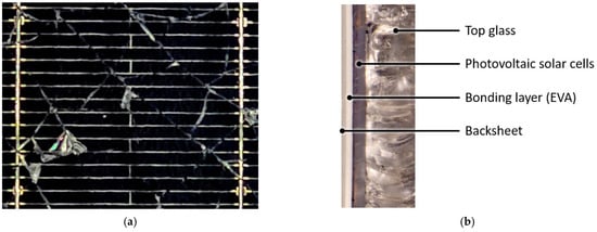
Figure 1.
Single-crystal silicon solar cell with broken glass layer, metal mesh, c-Si layer and back sheet: (a) view from the front side (tenfold magnification); (b) cross-section of the PV panel (thirtyfold magnification).
The specimens used in the electric resistive heating experiments consist of strips extracted from a PV panel, containing several individual cells (Figure 1a). These specimens include the semiconductor layer encapsulated within the adhesive material, copper interconnects, the supporting substrate, and the fractured glass layer (Figure 1b).
2.2. Electric Resistance Heating
The thermal behavior of the polymer layer and the semiconductor layer with an integrated metallic grid can be most reliably evaluated under electro-resistive heating conditions. However, the applied electric current must be maintained at a constant level to avoid overheating and potential failure of the metallic grid. Heating is initiated in the copper interconnects and busbars, leading to changes in the electrical conductivity of the semiconductor. As a result, the semiconductor begins to conduct electric current (Figure 2, thereby further enhancing the heating effect within the metallic grid.
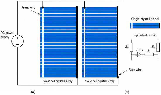
Figure 2.
A schematic of the resistive heating of the solar panel: (a) general connection diagram; (b) equivalent electrical circuit of a single cell.
Direct electric resistive heating is implemented using a specially designed clamping fixture for a longitudinal strip of the PV panel, with an effective working area of 55 × 95 mm. The strip width encompasses three busbars and approximately eight (2 × 4) individual cells. Both mechanical fixation and electric current supply are achieved using solid copper electrodes positioned at both ends of the strip. The terminal regions on both sides of the PV strip are prepared by removing the glass layer, ensuring proper electric contact for current injection into the three busbars via copper interconnect ribbons.
A direct current (DC) power supply is used for current control in the range of 1.0–1.2 A at a voltage of 15–20 V. Temperature measurements are carried out using a thermal imaging camera in combination with two thermocouples attached to the strip.
The equivalent circuit of a single cell is shown in Figure 2b. The equivalent circuit consists of the resistances of the connecting conductors (Rw) and the resistance of the doped silicon crystal (Rs). The Rs has the highest value and is therefore the dominant factor determining the current in the circuit and, consequently, the heating process.
In this configuration, the photovoltaic semiconductor elements play a stabilizing role, on the one hand defining the current level in the circuit, and on the other hand contributing to a more uniform heat distribution both within the bulk and across the surface of the entire panel.
The efficiency of electro-resistive heating of the layer is governed by the magnitude of the current supplied through the busbars. At I = 1 A the temperature reaches approximately 120–130 °C for about 30 s, whereas at I = 1.2 A within the same time period, it increases to approximately 140–150 °C. The presence of three longitudinal busbars results in a current distribution of approximately 0.3–0.4 A per busbar, as well as a voltage drop of about 5–7 V across each solar cell. Electrical breakdown, accompanied by melting of the Tedlar substrate and burnout of the metallic grid, occurs when the current is increased to approximately 5 A.
A relatively uniform heat distribution is achieved within the volume of the cell under this type of heating (Figure 3a), indicating that at this temperature the electric current is conducted not only through the metallic grid but also through the semiconductor itself. The p–n junction is activated upon heating, resulting in an increase in its electrical conductivity.
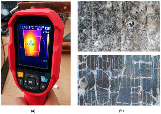
Figure 3.
Electric resistance heating of a strip of a PV panel: (a) temperature measurement during heating using a thermal imaging camera; (b) view of the strip after processing at different magnifications.
The structure of the semiconductor layer processed via electric resistive heating beneath the glass layer remains intact; no fragmentation is observed after the treatment, although local melting of the PVF substrate is detected in certain regions (Figure 3b).
To evaluate the effect of electric-resistive heating on the composite structure of the PV panel, it is necessary to determine the electric resistance of its current-carrying components, namely the busbar–finger grid and the behavior of the silicon semiconductor layer with a p–n junction. During electric resistive heating (Figure 3), a uniform heating of the silicon layer was observed, indicating that the semiconductor located between the grid and the aluminum foil increases its electrical conductivity.
2.3. Specific Temperature Dependencies of the Specific Resistance of Solar Cell Layer
The electric resistance was determined by direct measurement in the semiconductor layer of the photovoltaic structure after removal of the glass layer. The electric resistivity of the samples was measured using an Agilent 4294A (Santa Clara, CA, USA) impedance analyser combined with the 42941A impedance pin probe test fixture. An advanced I–V probing method for ultra-thin gate oxide impedance evaluation directly above the silicon panel was employed [21].
The tested crystalline samples had dimensions of 18 × 1 × 0.4 mm, where 0.4 mm corresponds to the sample thickness. A two-component equivalent circuit model (Rp–Cp) was used, where the electric resistivity was derived from the parallel resistive component Rp. The resulting resistivity was found to be 5.1–6.5 Ω·m, which is slightly higher than ρ0 of lightly doped crystalline silicon. This increased resistance may be attributed to the non-uniformity of the samples, microcracks, contamination, and surface contact resistance induced by mechanical damage during glass removal.
According to literature data, the conductivity of crystalline silicon ranges from approximately 0.001 Ω·m (heavily doped material) to 10 Ω·m (lightly doped material), reaching up to 23 kΩ·m for intrinsic (ultra-pure) silicon. In order to obtain the required electrical properties for photovoltaic applications (i.e., to form a p–n junction), monocrystalline, polycrystalline, or amorphous silicon layers are intentionally doped, typically with Sb donors for p-type silicon and P/B acceptors for n-type silicon. Doping increases the concentration of SiO2/SiO and CO/CO2 impurities, which reduces the conductivity of the pure monocrystalline layer to 1.8–2.0 Ω·m at the reference temperature [22].
The measurements were performed after mechanical removal of the glass layer and the EVA dielectric layer deposited on the silicon (Si) surface. The measured value of the specific electric resistivity of this layer at room temperature was ρ0 = 5.1–6.5 Ω·m, which is slightly higher than that of lightly doped crystalline silicon. The corresponding electric conductivity (σ0 = 1/ρ0) is σ0 = 0.15–0.20 S/m.
The increased resistivity is most likely attributed to the non-uniform thickness of the silicon layer fragments, the presence of microcracks, contamination, and surface contact resistance, all of which are induced by mechanical stress during glass removal.
The experimentally obtained values of the temperature-dependent electric resistivity ρ(T) during gradual heating up to 200 °C over approximately 150 s are presented in Figure 4.
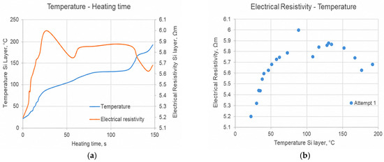
Figure 4.
Experimental results from the measurement of the specific resistivity of the doped semiconductor layer with a p–n junction on an undamaged sample with the glass layer removed (attempt 1): (a) temperature–time curve; (b) variation in specific electrical resistivity as a function of heating temperature.
Experimental results show that upon heating up to 200 °C, the electric resistivity of the doped silicon layer increases to a maximum value, ρmax. In the temperature range of 80–110 °C, a pronounced step-like change is observed, followed by a slight decrease. This behavior is most likely associated with the activation (turn-on) of the p–n junction within this temperature interval, which leads to an increase in its electrical conductivity.
While under normal photovoltaic operation—i.e., extraction of the electric energy generated by the p–n junction—it is important to consider the variation in its electric resistance at temperatures up to 80 °C; in the case of reverse current injection through the grid, the governing factor for the electric resistive heating process is the temperature dependence of the semiconductor layer above 100 °C.
Approximation of the experimental data, i.e., their formalization into a general mathematical relationship for the variation in specific resistivity, enables subsequent numerical simulation and detailed analysis, although not accounting for the step associated with p–n junction activation. Neglecting this transition-related discontinuity in the modeling of the photovoltaic semiconductor layer allows for improved agreement between the mathematical functions and the experimental results obtained during electric resistive heating.
Temperature dependencies of the specific resistivity in semiconductors are typically described by exponential relationships, either using a monotonically decaying function
or by an exponential saturation model as
where T is the heating temperature of the semiconductor in °C; ρmax is the maximum specific resistivity at 200 °C.
The data from both experiments were modelled using nonlinear regression, and the parameters of the relationships (1) and (2) were determined using the least-squares method. To assess the quality of the approximation, the coefficient of determination, R2, was calculated.
The third function (dashed line) for both experiments was obtained via log-linear extrapolation, based on the hypothesis that functions with high ρmax correspond to samples with significant structural modifications, those with intermediate ρmax correspond to samples with minor structural changes, and those with low ρmax correspond to samples without structural alterations, i.e., samples without mechanically removed glass layers.
The results regarding the parameters of the parallel dependencies corresponding to function (1) are as follows (Figure 5a):
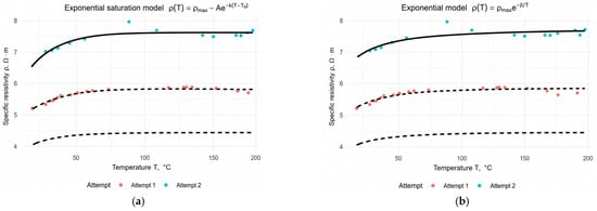
Figure 5.
Graphical representation of the numerical expressions describing the variation in specific resistivity for different coefficients of the exponential functions: (a) dependencies according to the model represented by function (1); (b) dependencies according to the model represented by function (2).
- -
- With high = 7.796 Ωm and = 3.072 (solid line), ;
- -
- With intermediate = 5.920 Ωm and = 2.663 (dotted), ;
- -
- With low = 4.495 Ωm and = 2.308 (dashed line).
Accordingly, the following parameters were obtained for expression (2) (Figure 5b):
- -
- With high = 7.641 Ωm, = 1.102 Ωm and = 0.05555 (solid line), and ;
- -
- With intermediate = 5.795 Ωm, = 0.6386 Ωm and = 0.05538 (dotted line), and ;
- -
- With low = 4.395 Ωm, = 0.370 Ωm and = 0.05521 (dashed line).
2.4. Specific Temperature Dependencies of the Conductive Metal Mesh (Busbars and Fingers)
The main role in electric-resistive heating is played by the metallic grid of fingers and busbars, which primarily conducts the electric current. Their geometric parameters—namely the cross-sectional area of the busbars and fingers, as well as the density of the metallic grid—determine both the current density () they carry and the distribution of the electric field intensity (E) within the semiconductor layer.
The silicon (Si) semiconductor layer mainly enables a relatively uniform temperature distribution; however, it also undergoes heating due to its partial electric conductivity.
The type of aluminium alloy used for the deposition of the metallic grid implies a linear temperature dependence of its electric resistance variation as
where T is the heating temperature of the alloy (°C); ρ0 is the specific electric resistivity at room temperature; and α is the temperature coefficient of electric resistivity.
The metallic grid in the solar cell consists of an Al–Si eutectic alloy, which is applied via screen printing and subsequent firing, resulting in a specific resistivity higher than that of pure aluminium. For the aluminium alloys used in solar cells, Matthiessen’s rule [23] is applied to determine the total resistivity, taking into account impurities in the aluminium paste as well as defects introduced during the firing process. According to literature data, the specific resistivity of such an alloy is in the range = 3.0 ÷ 6.5 × 10⁻⁸ Ω.m, which is two to three times higher than the corresponding values for technically pure aluminium, while the temperature coefficient governing this increase is = 0.0039 K−1.
3. Electric Resistance Heating Modeling
Simulation modeling of the electric resistive heating process of the photovoltaic structure for the purpose of delamination was implemented in COMSOL Multiphysics 5.4.0.388. The virtual model corresponds to a single cell of a crystalline silicon (c-Si) PV panel, which was also used in the experimental electric resistive heating studies.
A stationary study was selected, combined with a two-step parametric sweep (auxiliary sweep) of the terminal current magnitude over a time range between 30 and 60 s. The standard COMSOL Multiphysics modules were employed, namely Electric Currents and Heat Transfer in Solids, coupled via the Multiphysics interface, which includes Electromagnetic Heating and Temperature Coupling.
3.1. Definition of Geometry and Material Properties
A single unit cell with dimensions of 18 × 24 mm was implemented, incorporating all layers of the composite photovoltaic structure, as well as two busbars with an interconnecting network of aluminium-alloy fingers. The virtual model consists of the following main layers (Geometry):
- PVF (polyvinyl fluoride) Tedlar layer—with a thickness of 0.94 mm;
- Si cell p–n junction layer—with a thickness of 0.4 mm, suitable for thick-film Si panels with a thickness of 300–500 µm;
- EVA (ethylene-vinyl acetate) layers—two layers, each with a thickness of 0.04 mm (40 µm);
- Glass layer—with a thickness of 3.2 mm;
- Polymer composite material supporting the solar cells—with a thickness of 1.4 mm;
- Metallic grid composed of aluminium-alloy fingers (Al-alloy fingers) with a diameter of 0.03 mm and busbars with a diameter of 0.3 mm, deposited on the semiconductor from the glass side;
- Aluminium foil layer with a thickness of 0.04 mm, deposited on the opposite side of the semiconductor, facing the polymer layer.
The thickness of 400 µm selected for the simulation is suitable for the model of thick-film Si panels developed in COMSOL, which does not quite converge when an exponential function is introduced to describe the change in electrical resistance in thin silicon layers, for example, below 270 µm.
The material properties of the defined geometric elements were obtained from literature sources [24,25], the COMSOL material library, and in-house measurements, primarily concerning the variation in the electric resistance of the semiconductor layer with increasing temperature. The material properties of the virtual Silicon Solar Cell are shown in Table 1.

Table 1.
Definition of Materials Properties of the virtual Silicon Solar Cell.
The transition was introduced using exponential relationships, the derivation of which is described in Section 2.3. The specific electric resistivity of the aluminium alloy used for the busbars, fingers, and foil varies within the range = 3.0 ÷ 6.5 × 10⁻⁸ Ω.m (corresponding to an eutectic Al–Si alloy) and is implemented as a linear temperature dependence, as described in Section 2.4. The temperature-dependent variation in the electric resistivity of the solar cell layer is introduced via the Electric Currents module—Current Conservation interface.
3.2. Power Supply Implementation
The power supply of the single cell is provided by a constant current , applied via a terminal to the upper part of the two busbars, while grounding is applied on the opposite side to the aluminium foil using the standard Electric Currents module. The two current-carrying parts are not directly short-circuited; instead, they are separated by the silicon semiconductor layer, which is subjected to the electric field established between the fingers/busbars and the metallic foil.
Electric-resistive heating is implemented using the standard Electromagnetic Heating interface for a simulation time of 30 or 60 s, with terminal current values ranging from 0.1 to 0.8 A, corresponding to a resulting voltage of up to 14 V. Heat transfer between the layers is modelled using the Heat Transfer in Solids module, assuming an ambient temperature of 20 °C.
The finite element mesh is defined with different element sizes for the individual layers of the single cell as follows: Extra coarse for the glass layer and the semiconductor, Normal for the silicon semiconductor layer, and Finer for the EVA layers, the metallic grid, and the aluminium foil.
4. Results
The analysis of the electric resistive heating process of the photovoltaic panel was carried out by evaluating the behavior of the simulated virtual cell within the COMSOL Multiphysics environment. A key role in this process is played by the electrically conductive metallic components (busbars/fingers and the aluminium foil), which are not directly connected, as they are separated by the silicon (Si) semiconductor layer (with a p–n junction), which also conducts electric current and undergoes heating.
This virtual model does not include copper interconnectors, as the primary objective is to clarify the influence of the electrical conductivity of the doped semiconductor layer on the electric resistive heating process.
The simulation model was validated against the temperatures achieved during laboratory experiments within the volume of the PV panel strip for the corresponding magnitude of the applied current (Figure 4).
4.1. Temperature-Dependent Variation in the Electric Resistance of the Si Solar Cell Layer
The electric resistance of the intermediate semiconductor layer and the variation in its electric conductivity during the heating process influence the temperature reached by the cell. Based on the experimental results from the measurement of the specific resistivity of the semiconductor layer extracted from the photovoltaic structure, two exponential relationships, (1) and (2), were derived.
The experimental values were obtained after removal of the glass layer, which implies a certain degree of structural degradation of the semiconductor. Therefore, lower electric resistance values are expected for the doped silicon in an intact, fully assembled solar panel.
The variation in the electric resistance of the semiconductor layer was modeled using parallel forms of relationships (1) and (2) with different coefficients, i.e., with different maximum values of ρmax, but with similar exponential coefficients.
To determine the variation in the electric resistance within the unit cell, a computational probe point (Cut Point 3D) was defined in the software at the center of the semiconductor layer (i.e., at the p–n junction). This point is positioned between the elements of the metallic grid without direct electric contact with them.
The resulting variation in the specific electric conductivity with increasing temperature, evaluated at this point using both the primary and the parallel forms of the exponential relationships (1) and (2), is presented in Figure 6.
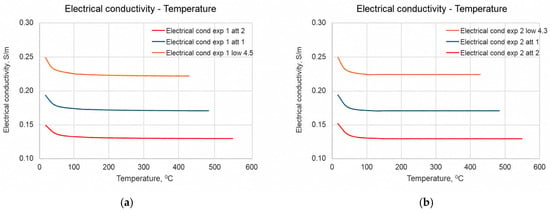
Figure 6.
Variation in the specific electric resistivity of the Si layer in the simulation of electric resistive heating of a single cell: (a) using exponential relationship (1); (b) using exponential relationship (2).
The variation in the specific electric conductivity as a function of temperature for the two types of exponential relationships indicates that there is no fundamental difference between the use of a monotonically decaying function of type (1) and an exponential saturation function of type (2), provided that they adequately represent the experimentally obtained values of electric resistance.
The temperature distribution within the volume of the unit cell at a terminal current of 0.5 A, for electric resistance corresponding to the two exponential relationships (1) and (2), is presented in Figure 7, where it is shown that the maximum temperature reached in both cases corresponds to the location of the semiconductor layer, while the heating of the remaining layers is mainly due to heat transfer from it.
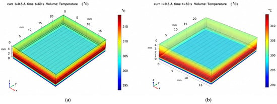
Figure 7.
Temperature distribution in a single solar cell during electric resistive heating at It = 0.5 A (attempt 1): (a) using relationship (1); (b) using relationship (2).
The maximum temperature shown in Figure 7 corresponds to a Si semiconductor layer thickness of 400 µm, which is the same as the thickness of the sample actually used in the laboratory experiments. If the thickness of the Si layer is reduced by 25%, i.e., from 400 µm to 300 µm, the maximum temperature decreases by 5% for every 100 µm of Si layer thickness. When using exponential relationship 1, then the maximum temperature drops from 315 °C to 300 °C, and when using relationship 2, it drops from 310 °C to 295 °C. This indicates that when using electric resistance heating for photovoltaic panels with a silicon layer, the metal grid plays a key role, while the silicon layer serves a stabilizing function.
As shown in Figure 7, for the same magnitude of the terminal current It, the type of exponential relationship introduced does not significantly affect the temperature achieved during electric resistive heating. When relationship (2) is used, the temperature is slightly lower than that obtained with relationship (1), namely by approximately 4 °C at It = 0.4 A, increasing to about 8 °C at It = 0.8 A.
The terminal voltage Ut exhibits a similar trend to the temperature, with the differences between the two relationships remaining minimal, within the range of 0.2 to 0.4 V.
Due to the small differences in the achieved temperature and the negligible deviations in the terminal voltage when using the two relationships, the subsequent analysis will consider only the specific electric resistivity of the semiconductor layer described by a monotonically decaying function, implemented through exponential relationship (1).
4.2. Distribution of the Electric Potential and Temperature Within the Cell
The terminal supply (i.e., of the two busbars of the virtual cell) with increasing current magnitudes in the range from 0.1 to 0.8 A corresponds to the range of the conducted experiments on the PV panel strip. The distribution of the electrical potential Uw within the cell volume and in a cross-section of the cell (Cut Line 3D) passing through one of the busbars is shown in Figure 8.
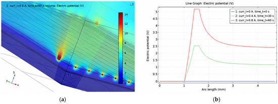
Figure 8.
Variation in electric potential in the single solar cell: (a) in the volume at terminal current = 0.8 A; (b) in the transverse line at terminal current between = 0.4 A and = 0.8 A.
The variation in the terminal current magnitude It determines the electric potential U and the temperature reached during electric resistive heating of the structure. A transverse line was introduced at the center of the cell in order to determine the temperature distribution across the cell cross-section. This line does not intersect the elements of the metallic grid of busbars and fingers, but passes through all structural layers of the cell.
The temperature distribution along this central transverse line of the cell cross-section, as well as the variation in the temperature gradient magnitude (Temperature gradient magnitude [K/mm]), are shown in the following Figure 9.
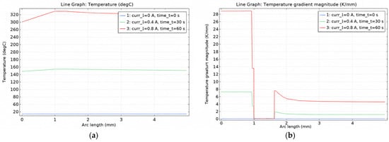
Figure 9.
Variation in temperature by electro-resistive heating in the transverse line of the single solar cell at terminal current between = 0.4 A and = 0.8 A: (a) temperature variation; (b) temperature gradient magnitude.
The temperature distribution in the cross-section of the single cell confirms the conclusion regarding the maximum temperature reached in the Si layer presented in the previous figure, while further complementing it with its variation in depth. A plateau is observed (Figure 9a), corresponding to the thickness of the Si layer, which is surrounded by a sharp temperature drop within the two EVA layers, followed by a gradual linear decrease in the glass layer and the supporting polymer.
A similar geometric distribution is observed in the evaluation of the temperature gradient across the cell cross-section (Figure 9b).
The heating of the intermediate Si layer is relatively uniform, while the heating of the remaining electrically non-conductive layers in the cross-section of the composite panel is governed by heat transfer from the semiconductor layer (Figure 9). The temperature reached in the aluminium-alloy busbars is slightly higher (by fractions of a degree) than that of the semiconductor layer.
The maximum temperatures that can be achieved during real heating for thermal delamination are limited by the eutectic phase transition (melting) temperature of the aluminium-alloy grid (577 °C), as defined in the Al–Si phase diagram, which also leads to local melting of the supporting polymer layer.
The obtained geometric distribution indicates that the increase in temperature within the Si layer, which in turn governs the heating of the two EVA layers, represents an optimal mechanism for heat delivery aimed at softening/melting the adhesive material and enabling subsequent thermo-mechanical delamination.
4.3. Variation in Current Density and Electric Field Intensity
The current–voltage characteristic between the variation in the terminal current magnitude [A] and the terminal voltage Ut [V], shown in Figure 10a, is linear. The magnitude of the applied terminal current also determines the variation in the temperature reached both in the metallic grid and in the intermediate semiconductor layer (Figure 10b). The temperature difference between the Al-alloy grid and the Si layer is negligible, reaching only 1–2 °C for It values above 0.5 A.
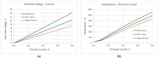
Figure 10.
Variation in the voltage in the metallic grid and the temperature of a single cell at different values of terminal current and electric resistance of the Si layer: (a) terminal voltage variability, (b) temperature variability.
From the graphs presented in Figure 10 it can be seen that the temperature of the single cell is primarily determined by the magnitude of the current supplied to the metallic grid; however, the maximum values of electric resistive heating also depend on the conductivity, i.e., on the manner in which the electric resistance of the intermediate semiconductor layer varies.
The variation in the terminal current magnitude [A] determines the current density J [A/mm2] in the busbars, and consequently in the fingers and the aluminium foil (Figure 11b). The current density in the electrically conductive components—primarily in the busbars of the metallic grid—as well as the electric field intensity between the two metallic layers (the grid and the foil), governs the heating of the PV panel. To represent the distribution of current density within the composite photovoltaic structure, a 3D visualization of the current density [A/mm2] within the volume of the unit cell was used (Figure 11a), along with a cross-sectional plot (Figure 11b).
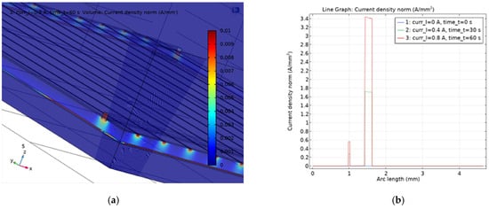
Figure 11.
Variation in the current density in the single solar cell: (a) in the volume at terminal current = 0.8 A; (b) in the transverse line at terminal current between = 0.4 A and = 0.8 A.
To represent the distribution of the current density [A/mm2] and the electric field intensity [V/mm], a mid-cross-section of the PV panel was used, passing through one of the busbars and the aluminium foil (Figure 11b).
The comparison of the variation in the current density in the busbar and in the aluminium foil with increasing terminal current magnitude (Figure 11), as well as the distribution of the electric field intensity in the semiconductor layer (Figure 8), confirms the conclusion from the laboratory experiment that the current supplied to the busbars determines the parameters of electro-resistive heating of the cell.
The temperature distribution during electro-resistive heating is, however, relatively uniform and depends on the characteristics of the individual layers of the PV panel (Figure 12). The maximum temperature values observed in the semiconductor layer are nearly equal to the heating of the metallic conductive components (metal grid and foil).
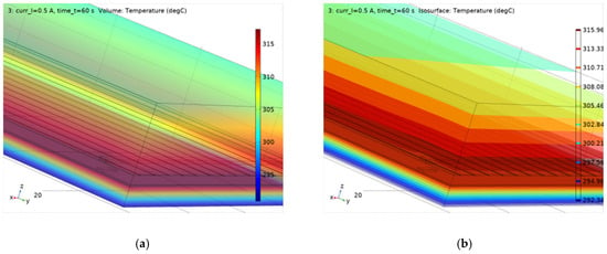
Figure 12.
Variation in the temperature in the single solar cell: (a) temperature distribution; (b) isotherms distribution.
The variation in the electric field intensity cross the individual layers of the PV panel as a function of the terminal current is presented in Figure 13.
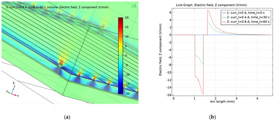
Figure 13.
Variation in the electric field intensity: (a) in the volume at terminal current = 0.8 A; (b) in the transverse line at terminal current between = 0.4 A and = 0.8 A.
The determined relationships between the achieved temperature and the terminal current are strictly linear (Figure 14), demonstrating the specific characteristics of the electric resistive heating process of the single cell.
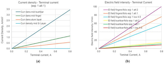
Figure 14.
Variation in current density and electric field intensity at different values of terminal current: (a) current density in the metallic grid and foil, (b) electric field intensity in the Si layer at different semiconductor resistivities.
The evaluation of the differences in electric field intensity between the two electrically conductive (metallic) components of the cell, located on both sides of the semiconductor layer, shows that significantly higher values of are observed at the fingers compared to the busbars. These differences increase with increasing terminal current and likely determine the growing contribution of the fingers to the electric resistive heating of the semiconductor layer.
5. Discussion
The determination of the temperature at different magnitudes of the terminal current supplied to the ends of the two busbars of a single-crystal silicon solar cell shows good agreement with the experimental results for values of = 0.3 ÷ 0.4 A.
The temperature of electric resistive heating of the semiconductor layer in the single-crystal silicon solar cell, , is primarily determined by the magnitude of the terminal current and, consequently, by the current density in the metallic grid. However, variations in the specific electric resistivity of the aluminium alloy of the busbars and fingers within the range = 3.0 ÷ 6.5 × 10⁻⁸ Ω.m (corresponding to an eutectic Al–Si alloy) do not significantly affect the achieved temperature or its distribution.
The maximum temperature values of the single cell achieved during electro-resistive heating depend on the electrical resistance of the intermediate semiconductor Si layer. At the same terminal current , variation in the maximum electric resistivity of the doped silicon layer changes the electric field intensity from 1.9 to 6.7 V/mm, resulting in an increase in the Si layer temperature from 141 °C to 274 °C (Figure 15b).
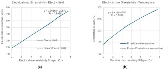
Figure 15.
Effect of the Si layer resistivity on the heating of the unit cell at a terminal current = 0.4 A on: (a) electric field intensity ; (b) maximum temperature achieved during electro-resistive heating.
From Figure 15a it can be seen that there is a linear dependence between the resistivity of the Si layer and the electric field intensity, similar to that observed for the terminal voltage Ut. In contrast, the maximum temperature reached in the Si layer, , exhibits an almost linear but still power-law-type dependence (Figure 15b). The current density in the metallic grid (busbars, fingers, and aluminium foil) is not affected by variations in the electric resistivity of the semiconductor layer, but depends solely on the magnitude of the applied terminal current .
The novelty of the present study lies in the utilization of direct current applied through the existing conductive network of the photovoltaic panel, enabling internally generated resistive heating without the need for external heating sources. Furthermore, the study combines experimental investigations with FEM-based multiphysics simulations, allowing detailed analysis and validation of the thermo-mechanical delamination process. An additional innovative aspect is the incorporation of temperature-dependent semiconductor conductivity into the numerical model, providing a more accurate representation of the electrical and thermal behavior of photovoltaic cells during heating and an additional validation of the process.
The proposed approach aims to contribute to the emerging field of low-impact next-generation photovoltaic recycling technologies, as it has the potential to offer advantages over conventional methods such as furnace heating, characterized by high thermal inertia, and chemical delamination processes, which generate hazardous chemical waste [26]. Unlike conventional external heating techniques (hot-air, furnace, infrared) or volumetric electromagnetic approaches (microwave/RF), the proposed method utilizes the intrinsic conductive architecture of the PV cell itself—including busbars, fingers, and the semiconductor layer—to generate localized internal heating directly within the multilayer structure. Such localized heating may reduce unnecessary thermal exposure of the module components, thereby decreasing overall energy demand and minimizing secondary degradation of recoverable materials. Another advantage of the proposed method is the absence of aggressive chemical reagents, representing a significant environmental advantage compared to solvent-based delamination methods.
The experimental observations indicate that the semiconductor layer remains structurally intact after heating within the investigated temperature range. The typical energy input for the investigated laboratory-scale samples was in the range of several hundred joules per heating cycle, corresponding to the range of 0.0001–0.001 kWh depending on the applied current and heating duration.
Nevertheless, additional investigations involving full-scale photovoltaic panels are required. In larger modules, potential challenges associated with heat distribution may arise, requiring higher energy input and electrical supply from multiple contact locations, particularly in cases involving degraded or partially damaged busbar networks. These aspects will be addressed in the next stage of the research. At the current stage of the study, no quantitative evaluation has yet been performed regarding the purity levels or the potential reuse quality of the separated fractions, including glass, silicon, metals, and polymeric materials, as such characterization is beyond the scope of the present work and will be conducted in future studies. A comprehensive assessment of the overall energy efficiency and the potential industrial applicability of the proposed process will be possible only after conducting experiments with different types of real-size photovoltaic panels.
6. Conclusions
The parameters of direct electric resistive heating were determined, and it was found that this approach provides the best results in terms of achieving an optimal temperature distribution in close proximity to the adhesive material and ensuring precise control of the heating process.
Through direct measurements of the semiconductor layer extracted from the photovoltaic structure after removal of the glass layer, it was confirmed that the electric resistance of the Si layer in the PV panel is structure-sensitive, i.e., dependent on its structural integrity, including mechanically induced defects and imperfections.
A relationship between the electric conductivity of the semiconductor layer in solar cells and the heating temperature for the p–n junction and a shift toward intrinsic conductivity was established. Two types of exponential dependencies were derived, analyzed, and compared through simulation modeling.
A virtual model of a single photovoltaic cell for a model of thick-film Si photovoltaic panels was developed in COMSOL Multiphysics, corresponding to the parameters of the composite material used in the real experiments. The model was analyzed and validated against the experimentally observed effects of electric resistive heating under laboratory conditions. The electric current parameters used to realize electric resistive heating of a PV panel strip were employed as input parameters and confirmed through simulation results.
Using the virtual model, it was established that, under specific terminal current conditions, identical geometrical features, and a given specific electric resistivity of the metallic grid, the electric conductivity of the semiconductor layer plays the dominant role in the electric resistive heating of the PV panel.
Author Contributions
Conceptualization, V.K. R.D., E.T. and M.Z.; methodology, V.K. R.D., E.T. and M.Z.; writing—original draft preparation, V.K. R.D., E.T. and M.Z.; software, M.Z., K.D., V.M., V.K. and D.A.; resources, M.Z., K.D., V.M., V.K. and D.A.; visualization, M.Z., K.D., V.M., V.K. and D.A.; validation, V.M., K.P., E.T., A.N., D.A. and K.D.; investigation, V.K., R.D., V.M., D.A. and A.N.; writing—review and editing, V.K., M.Z., K.P., V.M. and R.D.; supervision, E.T., Y.S., K.P. and R.D.; project administration, Y.S., K.D.; funding acquisition, Y.S. All authors have read and agreed to the published version of the manuscript.
Funding
This study is financed by the European Union-Next Generation EU, through the National Recovery and Resilience Plan of the Republic of Bulgaria, grant number: project № BG-RRP-2.004-0005.
Data Availability Statement
The original contributions presented in this study are included in the article. Further inquiries can be directed to the corresponding authors.
Conflicts of Interest
The authors declare no conflicts of interest.
Abbreviations
The following abbreviations are used in this manuscript:
| EVA | Ethylene-vinyl acetate |
| PV | Photovoltaic |
| PVF | Polyvinyl fluoride |
References
- Czepło, F.; Borowski, P.F. Innovation Solution in Photovoltaic Sector. Energies 2024, 17, 265. [Google Scholar] [CrossRef]
- Rynska, E. Review of PV Solar Energy Development 2011–2021 in Central European Countries. Energies 2022, 15, 8307. [Google Scholar] [CrossRef]
- Yamaguchi, M. Current Status and Future Direction of Photovoltaics. Appl. Sci. 2025, 15, 9416. [Google Scholar] [CrossRef]
- Ember. World Adds a Record-Breaking 814 GW of Solar and Wind in 2025. Available online: https://ember-energy.org/latest-updates/world-adds-a-record-breaking-814-gw-of-solar-and-wind-in-2025/ (accessed on 17 April 2026).
- Stone, S. “Unlike Anything Seen Before”: Record 814 GW of New Solar and Wind Installed Globally in 2025. BusinessGreen, 20 March 2026. Available online: https://www.businessgreen.com/news/4527230/unlike-seen-record-814gw-solar-wind-installed-globally-2025/ (accessed on 17 April 2026).
- European Commission; Eurostat. Solar: Main Source of EU Electricity in June with 22%. Eurostat News Release, 29 September 2025. Available online: https://ec.europa.eu/eurostat/web/products-eurostat-news/w/ddn-20250929-3 (accessed on 17 April 2026).
- Gerold, E.; Antrekowitsch, H. Advancements and Challenges in Photovoltaic Cell Recycling: A Comprehensive Review. Sustainability 2024, 16, 2542. [Google Scholar] [CrossRef]
- Franco, M.A.; Groesser, S.N. A Systematic Literature Review of the Solar Photovoltaic Value Chain for a Circular Economy. Sustainability 2021, 13, 9615. [Google Scholar] [CrossRef]
- Islam, M.T.; Iyer-Raniga, U.; Trewick, S. Recycling Perspectives of Circular Business Models: A Review. Recycling 2022, 7, 79. [Google Scholar] [CrossRef]
- Mulazzani, A.; Eleftheriadis, P.; Leva, S. Recycling c-Si PV Modules: A Review, a Proposed Energy Model and a Manufacturing Comparison. Energies 2022, 15, 8419. [Google Scholar] [CrossRef]
- Todorov, G.; Vasilev, H.; Kamberov, K.; Ivanov, T.; Sofronov, Y. Concept and Virtual Prototyping of Cooling Module for Photovoltaic System. In Proceedings of the 2021 6th International Symposium on Environment-Friendly Energies and Applications (EFEA), Sofia, Bulgaria, 24–26 March 2021; pp. 1–4. [Google Scholar] [CrossRef]
- Chen, P.-H.; Chen, W.-S.; Lee, C.-H.; Wu, J.-Y. Comprehensive Review of Crystalline Silicon Solar Panel Recycling: From Historical Context to Advanced Techniques. Sustainability 2024, 16, 60. [Google Scholar] [CrossRef]
- Liu, S.; Ma, C.; Wang, X.; Lu, S.; Zhang, L.; Wang, Y.; Arzikulov, E. Manufacturing and Application of Glass Fiber Composites Based on CNT Films: Resistance Heating Curing, Health Monitoring and Deicing. Polym. Compos. 2025, 16, 5477. [Google Scholar] [CrossRef]
- Yue, C.; Zhang, Y.; Lu, W.; Zhang, Y.; Wang, P.; Li, Y.; Zhou, H. Realizing the curing of polymer composite materials by using electrical resistance heating: A review. Compos. Part A Appl. Sci. Manuf. 2022, 163, 107181. [Google Scholar] [CrossRef]
- Rahimi, R.; Krol, M. Optimizing electrical resistance heating using a combined modeling approach. Geosci. Can. 2025, 52, 217. [Google Scholar]
- Ghahremani, A.; Adams, S.D.; Norton, M.; Khoo, S.Y.; Kouzani, A.Z. Delamination Techniques of Waste Solar Panels: A Review. Clean Technol. 2024, 6, 280–298. [Google Scholar] [CrossRef]
- Calero, M.; Ramírez-Cantero, J.; Pérez-Huertas, S.; Pérez, A.; Mateos, M.; Blázquez, G. Recycling end-of-life solar panels: A comparative study of thermal and solvent delamination techniques. Sol. Energy Mater. Sol. Cells 2026, 295, 113990. [Google Scholar] [CrossRef]
- Zagorski, M.; Dimitrov, K.; Kamburov, V.; Nikolov, A.; Stoichkov, K.; Stoyanova, Y. An Innovative Approach for Delamination of Solar Panels Using a Heated Metal Wire. Recycling 2025, 10, 104. [Google Scholar] [CrossRef]
- Utility Model BG 5054 U1. Device for Delaminating Single-Sided Photovoltaic Panels. Available online: https://portal.bpo.bg/bpo-registers/utility-models/view/BG_U_2025_6403 (accessed on 17 April 2026).
- Kamburov, V.; Nikolov, A.; Ganchev, D.; Dimitrova, R.; Chernev, G.; Kandeva, M.; Petrov, K. Simulation modeling of the multistage differential bending process of photovoltaic module composite materials. AIP Conf. Proc. 2025, 3274, 070005. [Google Scholar] [CrossRef]
- Agilent Technologies Inc. Agilent Evaluation of MOS Capacitor Oxide C-V Characteristics Using the Agilent 4294A, Application Note 4294-3, 2004. Available online: https://seabaugh.nd.edu/assets/330850/at_man_agilent4294a_moscapacitoroxidec_vchar.pdf (accessed on 17 April 2026).
- Cibira, G. Silicon Resistivity Behaviour. Opt. Optoelectron. 2021, 19, 179–185. [Google Scholar] [CrossRef]
- Blatt, F. Matthiessen’s Rule. In AccessScience; McGraw Hill: New York, NY, USA, 2026. [Google Scholar] [CrossRef]
- Peter, N.; Kabu, O.; Stephen, K.; Antony, D. 3D Finite Element Method Modeling and Simulation of the Temperature of Crystalline Photovoltaic Module. Int. J. Res. Eng. Technol. 2015, 4, 378–384. [Google Scholar] [CrossRef]
- Alami, Y.; Rami, M.; Hajjaj, C.; Benhmida, M.; Faize, A.; Baghaz, E. Three-dimensional thermal modeling and analysis of the heat source, the impact of encapsulation materials and the back sheet of silicon PV modules. Appl. Therm. Eng. 2025, 280, 128430. [Google Scholar] [CrossRef]
- Kiskira, K.; Gerolimos, N.; Priniotakis, G.; Nikolopoulos, D. Life-Cycle Assessment of Innovative Industrial Processes for Photovoltaic Production: Process-Level LCIs, Scale-Up Dynamics, and Recycling Implications. Appl. Sci. 2026, 16, 501. [Google Scholar] [CrossRef]


Disclaimer/Publisher’s Note: The statements, opinions and data contained in all publications are solely those of the individual author(s) and contributor(s) and not of MDPI and/or the editor(s). MDPI and/or the editor(s) disclaim responsibility for any injury to people or property resulting from any ideas, methods, instructions or products referred to in the content. |
© 2026 by the authors. Licensee MDPI, Basel, Switzerland. This article is an open access article distributed under the terms and conditions of the Creative Commons Attribution (CC BY) license.