


Abstract
This study focuses on the impact of plasma-enhanced chemical vapor deposition (PECVD) synthesis parameters on the characteristics of a synthesized vertical array of multi-walled carbon nanotubes (VMWCNT). Catalytic synthesis is carried out on a thin nickel film on a silicon substrate after breakup of the Ni film into nanoparticles during pretreatments–oxidation and reduction. The influence of growth temperature, synthesis duration, plasma parameters, working pressure, and precursor concentration on the morphology and geometry of VMWCNT is investigated. A detailed combination of scanning electron microscopy, Raman spectroscopy, and X-ray photoelectron spectroscopy (XPS) is used to analyze the evolution of geometry, defect density, and nitrogen doping of carbon nanotubes (CNT) with varying synthesis temperatures. The work includes recommendations for adapting PECVD synthesis to achieve predictable and reproducible growth of VMWCNT with optimal properties for specific technological applications.
1. Introduction
The discovery of carbon nanotubes (CNT) by Iijima in 1991 marked the beginning of a new era in nanotechnology [1]. Among them, multi-walled carbon nanotubes (MWCNT), comprising multiple concentric graphene cylinders, have garnered immense interest due to their exceptional mechanical strength, remarkable electrical and thermal conductivity, and high chemical stability [2]. These properties make them ideal candidates for numerous applications, including reinforced polymer composites [3], field emission sources [4], thermal interfaces [5], supercapacitor and battery electrodes [6], chemical sensors [7], and nanoelectronic components [8].
To date, numerous technological approaches to the synthesis of low-dimensional carbon materials have been developed. For example, the classic arc discharge synthesis involves the use of an electric arc between graphite electrodes in an inert gas environment (helium or argon) to vaporize carbon and subsequently form high-density carbon clusters [9]. Despite its low yield and the difficulty of scaling up the process, this technology enables the production of single-walled, few-walled, and multi-walled carbon nanotubes, as well as high-purity graphene, at relatively low cost. Another approach is laser ablation, in which a graphite target is irradiated with powerful pulses or a continuous laser, causing the material to evaporate from the target due to intense localized heating by the laser beam [10]. Significant improvements in the production of single-walled carbon nanotubes became possible after the addition of metal catalysts (nickel and cobalt) to the graphite target, whereas the ablation of pure graphite resulted in other forms of carbon, such as diamonds, fullerenes, and amorphous carbon.
Today, the most widely used approach is chemical vapor deposition (CVD), considered the most promising method due to its flexibility and adaptability to various tasks, scale-up approach, and the fact that the quality of the resulting nanotubes meets the requirements for use in electronics [11]. The synthesis of CNT via the CVD method involves a two-step process: preliminary preparation of the catalyst (e.g., iron, cobalt, nickel, etc.) and the actual synthesis of the nanotubes. A key feature of the synthesis is the decomposition of carbon-rich precursor gases (typically CH4, C2H2, C2H4), which serve as the carbon source for CNT growth. Based on the method of reactant activation, CVD methods are divided into thermal CVD (using the thermal energy of the reactor) and plasma-enhanced CVD (PECVD). It is worth noting that PECVD synthesis is the only method that produces arrays of vertically aligned carbon nanotubes (VACNT) that are grown on a substrate according to a specified topology, controls the alignment and orientation of the CNT, and also enables synthesis at relatively low temperatures, which is critically important for integration with specific substrates and micro/nanoelectronic processes [12]. In addition, the PECVD method is compatible with existing integrated circuit manufacturing technologies, which suggests that it can be scaled up for mass production. In any case, each of the technological approaches listed above has both advantages and limitations, and the method chosen depends on the required quality of the MWCNT and the output volume. The term “quality” in this context encompasses several key metrics [2]:
- Structural crystallinity: The degree of graphitic order, evaluated as the density of defects (vacancies, pentagon–heptagon pairs) within the graphene lattice;
- Morphology: Including average diameter and diameter distribution, number of walls, length, and alignment (e.g., random networks vs. vertically aligned forests);
- Purity: The proportion of MWCNT relative to by-products like amorphous carbon and residual catalyst particles;
- Yield: The total mass or volume of MWCNT produced per unit time or per unit catalyst area.
The quality of the resulting MWCNT is not inherent but is meticulously dictated by the complex interplay of numerous technological parameters of synthesis. A slight variation in a single parameter can alter the growth kinetics and thermodynamics, leading to vastly different outcomes. Therefore, a deep and systematic understanding of the cause–effect relationship between these parameters and the final nanotube quality is paramount.
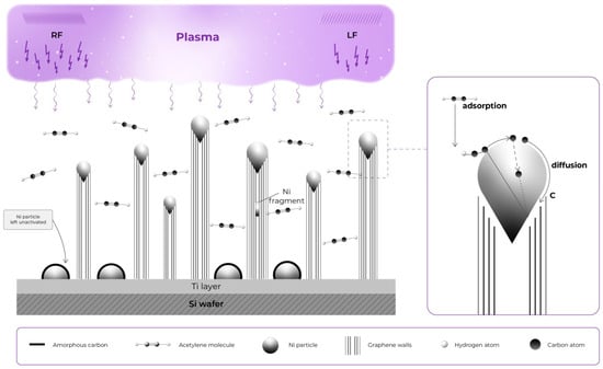
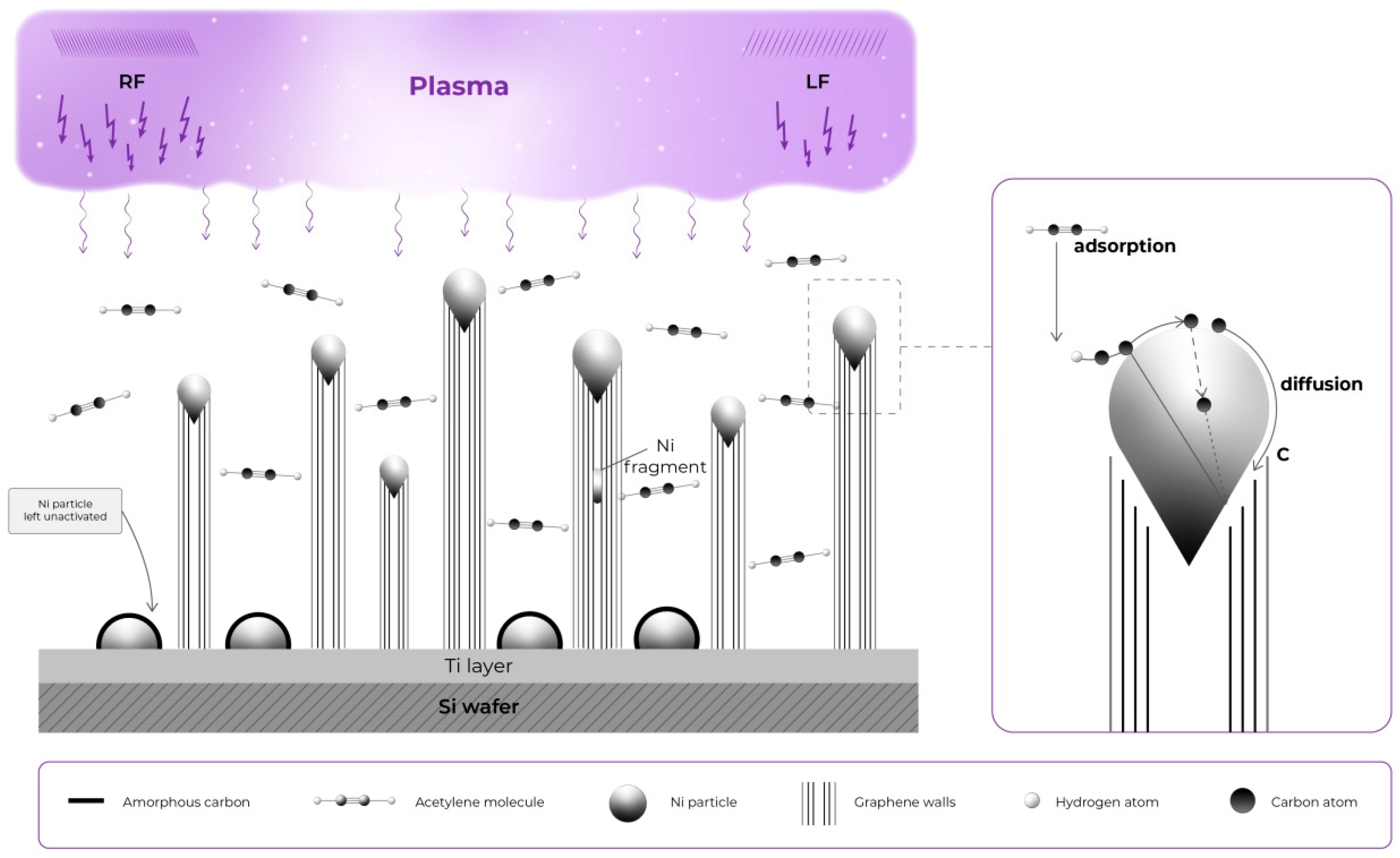
This article aims to provide a comprehensive and detailed experimental demonstration of how the fundamental technological parameters in PECVD synthesis govern the growth mechanisms and determine the structural and morphological quality of vertically aligned MWCNT (Figure 1).
Figure 1.
Schematic process of the VMWCNT synthesis.
The key synthesis parameters include substrate selection, catalyst selection, plasma type and source, plasma power (high-frequency, RF, and low-frequency, LF), operating pressure, temperature, and synthesis duration. We will examine the individual and synergistic effects of each parameter, drawing on experimental data, to provide a comprehensive guide to process optimization.
2. Materials and Methods
Silicon wafers with <100> crystal orientation were used as substrates for the research. A 10 nm Ti underlayer and a 2 nm Ni catalyst layer (99.995% and 99.98% purity (Angstrom Engineering Inc., Cambridge, ON, Canada)) were sequentially deposited through electron beam evaporation.
The growth of MWCNT was performed using a “PlasmaLab System 100” platform (Oxford Instruments plc, Abingdon, UK). The gas reagents O2 (Air Liquide S.A., Paris, France, 99.999%), He (Air Liquide S.A., Paris, France, 99.999%), NH3 (Air Liquide S.A., Paris, France, 99.999%), C2H2 (Air Liquide S.A., Paris, France, 99.5%), and H2 (Air Liquide S.A., Paris, France, 99.9999%) were fed into the Gas-Pod, and the homogeneous mixture was then fed into the process chamber. During the synthesis process, both during the pretreatment stages and during VMWCNT growth, built-in LF (450 kHz) and RF (13.56 MHz) plasma generators were used.
Under standard conditions, the decomposition of a thin catalyst film into particles requires only an increase in temperature. However, in our case, the nickel used as a catalyst must be deposited on an additional sublayer to prevent its interaction with the substrate and the formation of silicide, as well as, in general, with other materials on the sample surface. For this purpose, an additional titanium sublayer is introduced. Titanium and nickel have a phase diagram with complex behavior and can form intermetallic compounds of various compositions, which prevents the decomposition of nickel into individual particles and, consequently, the synthesis of CNT. Our previous studies [13] led to the recommendation of the following sequence of steps for VMWCNT synthesis: oxidation of the catalytic pair, reduction with the formation of nickel catalytic nanoparticles, and direct VMWCNT synthesis. After oxidation, titanium and nickel oxide layers are produced. The reduction process results in the reduction of nickel only; titanium remains as an oxide and acts as an inert layer for the formation of a structured array of nickel nanoparticles (for more details, please see ref. [13]). Hence, the sequence of oxidation–reduction allows the formation of an array of nickel nanoparticles with a uniform size distribution due to the fact that nickel and titanium have different energies for the formation and reduction of their oxides.
Based on these data, an initial process was developed in which VMWCNT arrays grow; the parameters of this process were then modified to determine the influence of specific factors on the characteristics of the carbon nanotube array. Silicon substrates were selected for the experiments because they are standard in microelectronics, readily available, resistant to high temperatures, the gases used in the synthesis, and plasma exposure, and because they are of stable quality with a highly polished surface, thereby ensuring that they do not introduce distortions into the results of the VMWCNT synthesis. The parameters of the main process are given in Table 1. The annealing temperature in the reduction process was equal to the synthesis temperature in all cases.
Table 1.
Main technological parameters of the pretreatment and synthesis processes for carbon nanotubes.
The characteristics of the VMWCNT were investigated using several characterization techniques. The geometry and morphology of arrays and individual nanotubes were observed using scanning electron microscopes (JSM-6010PLUS/LA (JEOL Ltd., Akishima, Japan) and Helios NanoLab 650i DualBeam electron-ion scanning microscope (FEI Company, Hillsboro, OR, USA)) and the JEM-2100 Plus transmission electron microscope (JEOL Ltd., Akishima, Japan). The crystal structure was identified using a Raman spectrometer Jobin Yvon HR 800 (HORIBA, Ltd., Kyoto, Japan) equipped with an Ar+ laser (514.5 nm) with low laser power (0.125 mW). The ID/IG ratio was used as a criterion for identifying defects in the VMWCNT [14,15]. The XPS studies were performed to identify the major forms of nitrogen, carbon, and oxygen in the VMWCNT structure using a Multi-Technique Scanning XPS Microprobe PHI Quantera SXM (Physical Electronics, Inc. (PHI), Chanhassen, MN, USA) with PHOIBOS 150 SPECS Surface Nano Analysis GmbH, Berlin, Germany) hemispherical analyzer (monochromatic Al Kα radiation with a photon energy of 1486.61 eV; end resolution of ∆E = 0.2 eV). All XPS spectra were obtained in fixed analyzer transmission mode, with pass energy of 120 eV for the survey spectra and 40 eV for separated lines. Plasma characteristics were measured using a C10346 multi-range plasma process monitor (Hamamatsu Photonics K.K., Hamamatsu, Japan).
3. Results
This section presents the results of a study examining the dependence of the morphology of synthesized VMWCNT arrays on the main process parameters: temperature, duration, the ratio of high-frequency to low-frequency plasma power, chamber pressure, and the flow rate of the carbon-containing gas. To determine the contribution of each individual parameter to the synthesis result, all process parameters except for the one under investigation were fixed and are summarized in Table 1.
3.1. The Effect of Synthesis Temperature on VMWCNT Growth
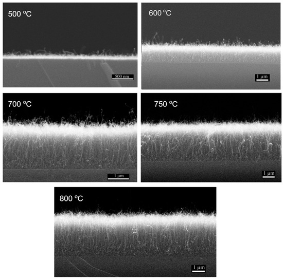
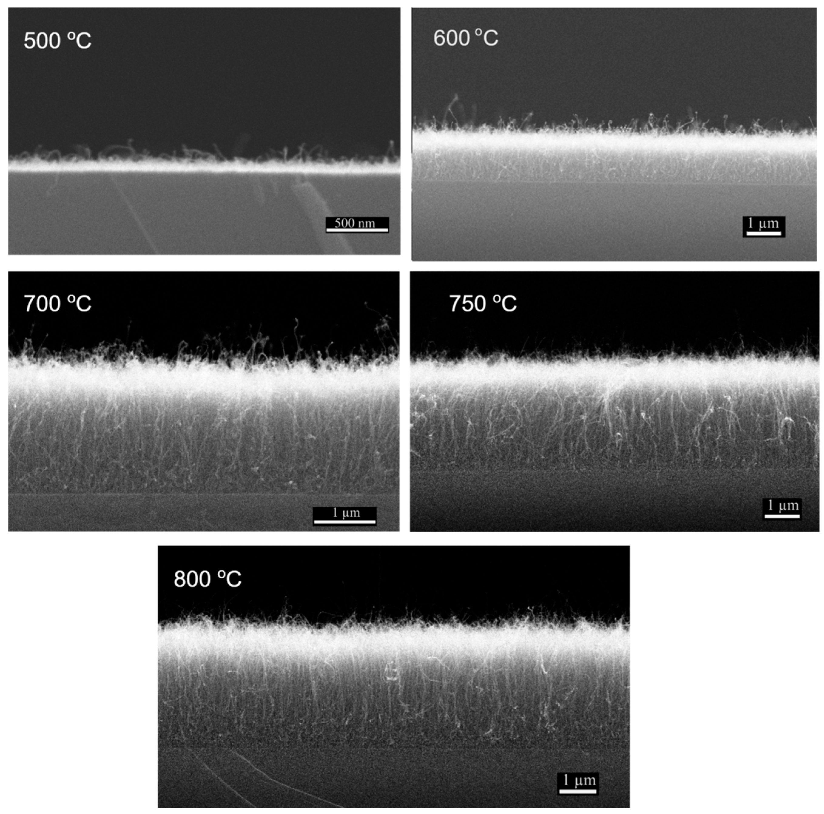
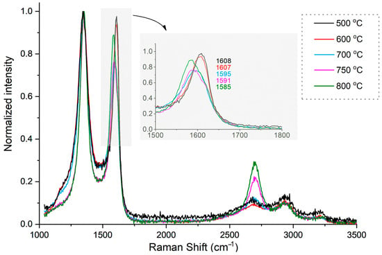
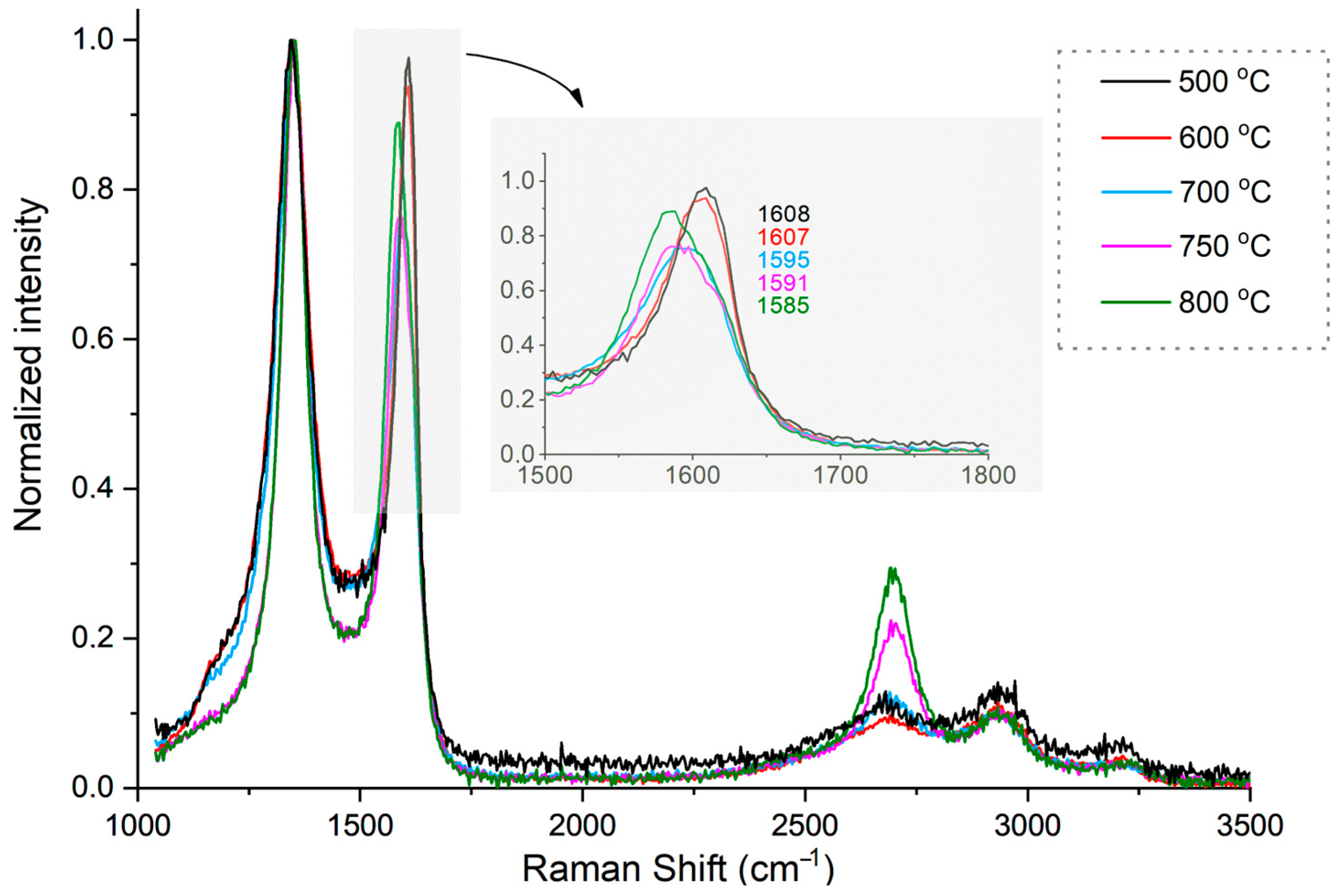
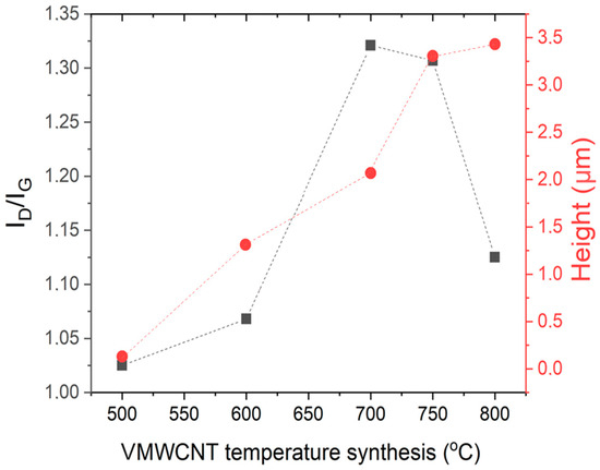
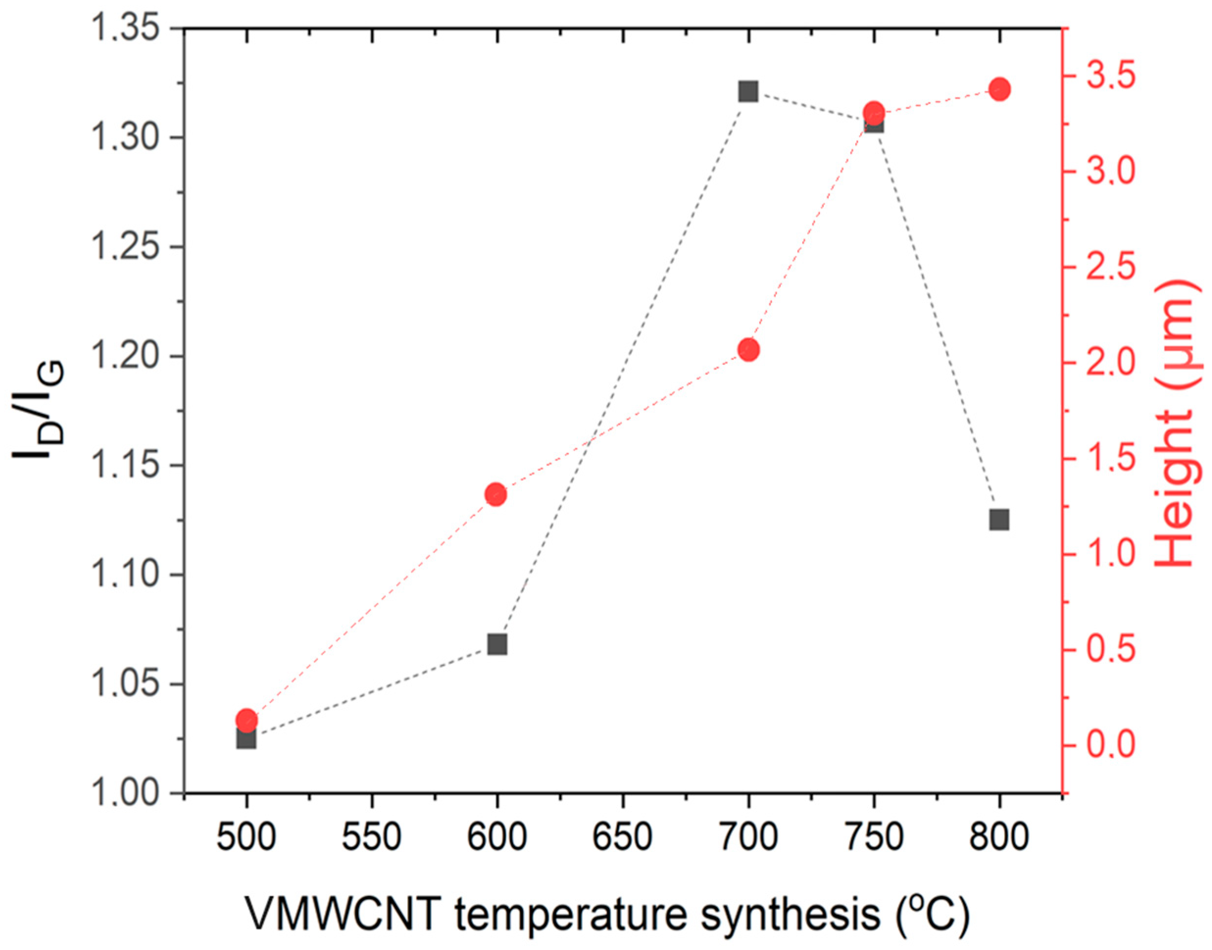
As a first step, an experimental study was conducted to investigate the dependence of the height of VMWCNT arrays on temperature during the synthesis process in the range of 500 °C to 800 °C. In previous studies [13], it was found that for a Ni catalytic layer thickness of 2 nm, a temperature of 500–550 °C is sufficient to initiate synthesis. As the thickness of the catalytic layer increases, the temperature at which it decomposes into individual nanoparticles and the size of the nanoparticles increase, and, accordingly, the synthesis temperature rises. At a constant nickel layer thickness, higher temperature leads to an increase in the height of the VMWCNT array. SEM images of the synthesized arrays are given in Figure 2, and Raman spectra are shown in Figure 3. Figure 4 reflects the correlation between the height of the VMWCNT array and the defect density of the nanotubes.
Figure 2.
SEM images of VMWCNT arrays synthesized at different temperatures (synthesis time 5 min; plasma mode PRF = 20 W, PLF = 30 W; working pressure 3 Torr).
Figure 3.
Raman spectra of VMWCNT arrays synthesized at different temperatures (synthesis time 5 min; plasma mode PRF = 20 W, PLF = 30 W; working pressure 3 Torr).
Figure 4.
The relationship between VMWCNT height and quality at different synthesis temperatures (synthesis time 5 min; plasma mode PRF = 20 W, PLF = 30 W; working pressure 3 Torr).
Figure 2 shows that as the temperature rises, not only does the final height of the VMWCNT array increase, but its morphology also changes significantly, specifically in terms of greater alignment and density. At a synthesis temperature of 500 °C (or lower), nanotube growth is significantly limited: only a few curved nanotubes are visible against the background of a sparse array at the initial stage of growth. Furthermore, at 700 °C, the height of the array increases noticeably, and, at 750 °C, the MWCNT array becomes more oriented perpendicular to the substrate. We attribute the higher proportion of amorphous carbon during low-temperature synthesis (the region of rising Raman intensity at 1500 cm−1) both to the increased defect density of the nanotubes themselves and the amorphous carbon covering the catalyst particles on the substrate that did not become VMWCNT nucleation sites and are visible due to the low height of the array.
A typical Raman spectrum of a PECVD VMWCNT array (Figure 3) includes the main characteristic combination modes and overtones: a defect-induced D line at approximately 1350 cm−1, an intervalley double-resonance process involving iTO phonons near the K-point of the Brillouin zone; the G line in the 1580–1590 cm−1 region, that is, first-order Raman allowed the E2g mode from in-plane stretching of sp2-bonded carbon atoms at the Г-point; the 2D line at approximately 2690 cm−1, arising from a double resonance mechanism involving two antiparallel phonons near the K-point of the Brillouin zone; the defect-activated D+D′ line at 2930 cm−1; and the 2D′ band near 3200 cm−1 associated with an intravalley two-phonon process involving longitudinal optical phonons [16,17]. The results obtained are consistent with known literature data for graphite-like materials [16,18]. The primary quantitative indicator of the defect density is the ID/IG ratio (Figure 4); specifically, the higher the ID intensity relative to IG, the greater the amount of disordered carbon present in the sample [19,20].
In [21,22], it was noted that PECVD synthesis results in the formation of more defective carbon nanotubes compared to conventional CVD due to the relatively low temperatures involved. In our case, the ID/IG ratio ranged from 1 to 1.35, which can be considered an optimal trade-off between defect density and height for CNT obtained via plasma synthesis for the selective growth of nanotubes in microelectronics-compatible processes. To understand the effect of temperature, it is more accurate to describe the dynamics of structural changes in VMWCNT as the temperature drops. In this case, the increase in the ID/IG ratio from 800 °C to 700 °C characterizes a decrease in the size of the nanocrystallite (La) and the inclusion of various carbon surface defects (such as vacancies, bends, Stone–Wales defects, amorphous phase, etc.) [23,24].
However, the sharp drop in the ID/IG ratio between 700 °C and 500 °C, though it may intuitively appear to indicate an improvement in the morphology of the VMWCNT, should not be taken as conclusive evidence. To clarify the results, it is necessary to examine several features in the graph that together form a coherent picture. Synthesis at 500 °C is characterized by higher defect density and amorphization, which is confirmed both by SEM images and by the presence of spectral contributions from modes at ~1200 cm−1 (the left shoulder of the D mode) and 1500 cm−1, associated with the inclusion of sp3 carbon and amorphous carbon [25,26].
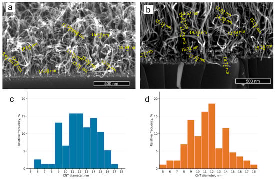
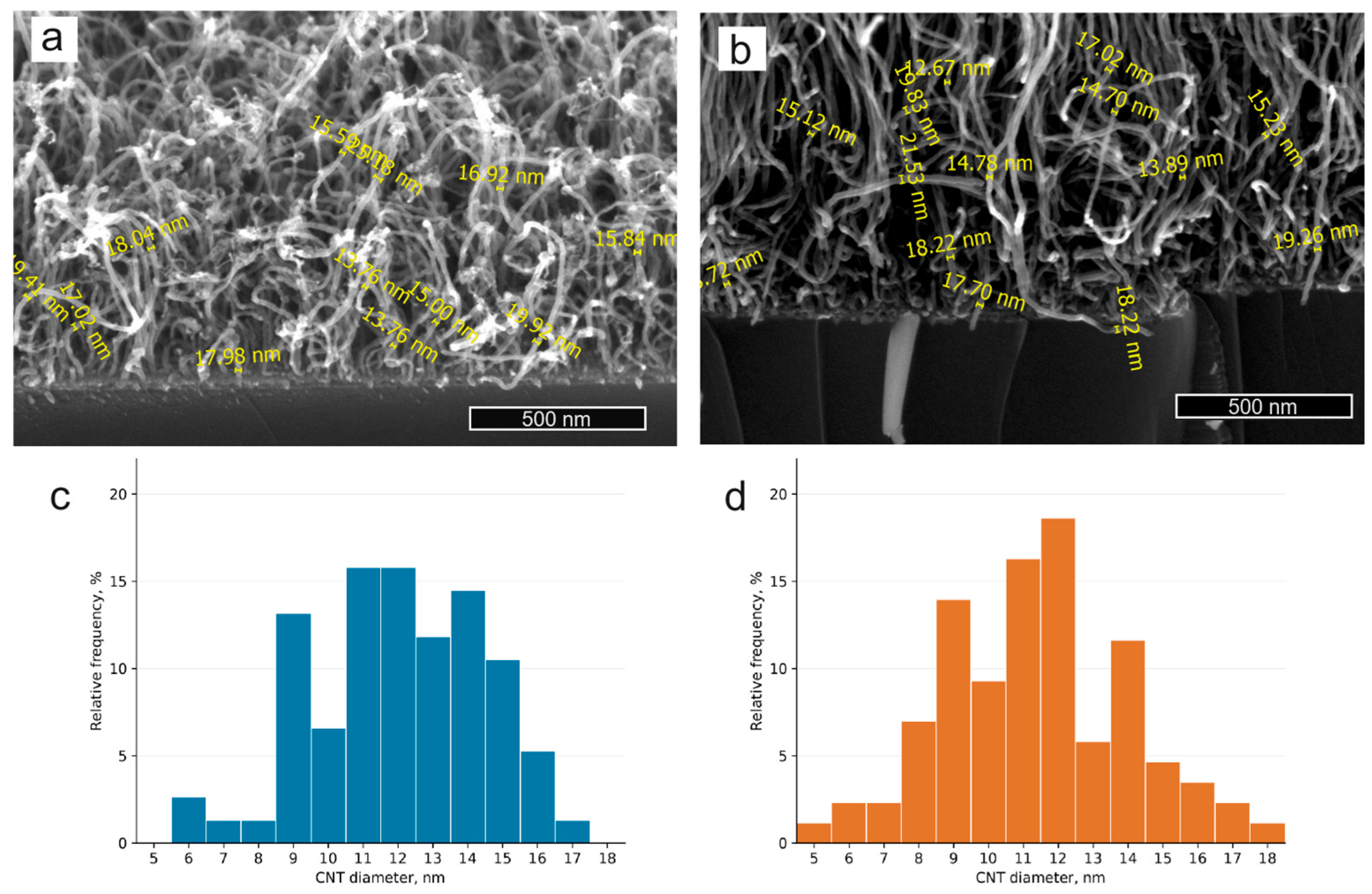
The best graphitization quality for VMWCNT was obtained at temperatures of 750 and 800 °C, as evidenced by the shift of the G band to 1580 cm−1, the decrease in the contribution of the peak at 1500 cm−1, and the absence of a shoulder at 1200 cm−1. An additional factor characterizing the structural features of VMWCNT is the 2D mode, which narrows and becomes more intense at synthesis temperatures of 750 and 800 °C, which is interpreted as an improved graphitic ordering. We suppose that in a taller, better-aligned array, the spectral contribution from thin-walled CNT increases because the major part of the signal is picked up from the top of the array, where the longest, thinnest, and finest CNT are located. Concurrently, a narrowing of the D mode is observed, suggesting the exclusion of multiple types of defects and that defects from distortion (visible in SEM, Figure 5) and bending (Stone–Wales defects, 5- and 7-membered rings) likely prevail [27].
Figure 5.
SEM characterization of VMWCNT synthesized at temperatures of 600 °C (a) and 800 °C (b) (synthesis time 5 min; plasma mode PRF = 20 W, PLF = 30 W; working pressure 3 Torr) with CNT diameter distribution (c,d), respectively. SEM images were taken at an angle of 52 degrees.
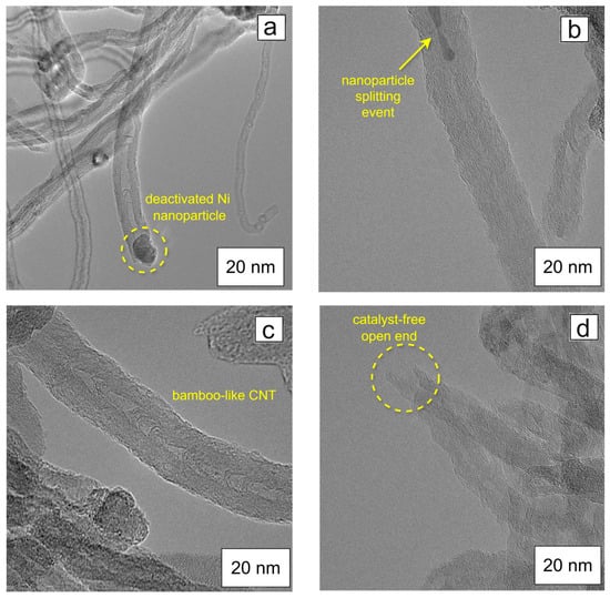
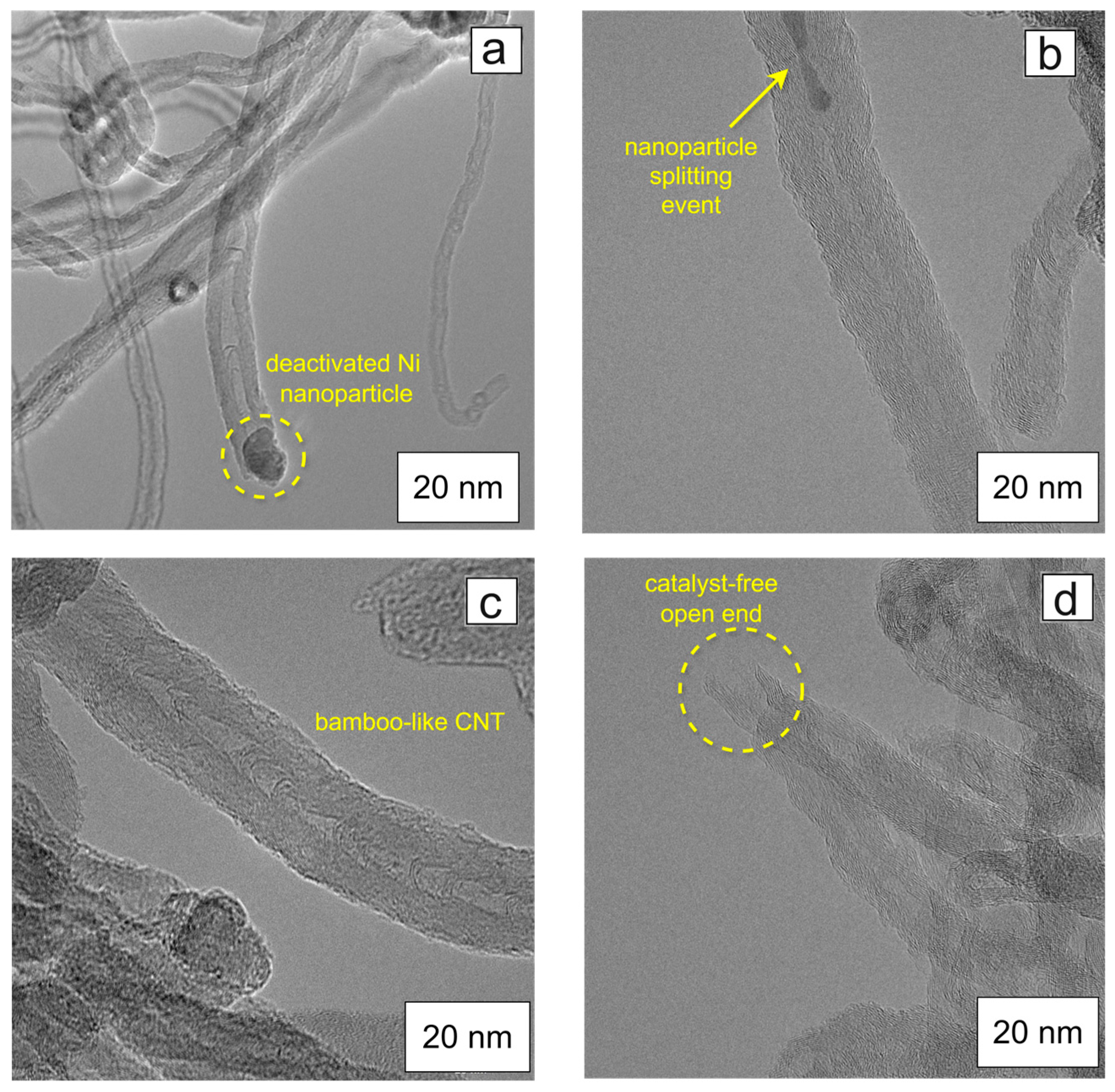
As shown in Figure 6, under our synthesis conditions using a nickel catalyst, only the growth mechanism leading to the formation of carbon nanotubes with a bamboo-like morphology is realized. No other CNT structure is formed in this system due to the specific behavior of the catalyst particle during growth.
Figure 6.
TEM characterization of VMWCNT synthesized at 700 °C on Ni catalyst by PECVD: catalyst deactivation during carbon nanotubes growth due to poisoning of catalyst nanoparticles (a); before encapsulation and deactivation the catalyst nanoparticle undergoes several stages of cleavage (b); typical experimentally obtained bamboo-like CNT (c) and the open end of the CNT, resulting from the release of the catalyst nanoparticle (d).
Visual confirmation of this can be found in [28], where the growth of bamboo-like CNTs on a nickel catalyst was monitored in situ in real time using transmission electron microscopy. The video recordings obtained by Lin P.A. and colleagues clearly show the key moment in the formation of the internal bridge: it occurs when an elongated (stretched) nickel nanoparticle, moving upward within the growing nanotube, leaves behind a closed graphene partition. Thus, each internal cavity of the bamboo-like structure corresponds to one “step” of catalyst movement along the tube axis.
Our TEM images demonstrate the internal structure of the CNT, revealing bamboo-like bridges, catalytic nickel particles, and synthesis termination patterns with encapsulated and released catalyst nanoparticles. The presence of an internal cavities/graphene partition allows us to assume the presence of trapped encapsulated molecular nitrogen, as detected by the XPS data (see below).
The synthesis temperature has a decisive influence on both the total nitrogen concentration in carbon nanotubes and the ratio of its configurations in the graphene lattice. According to the results of the XPS (Table 2), the dependence of the total nitrogen content in CNT is nonlinear. In this case, the fraction of graphitic (substitutional) nitrogen, in which the N atom occupies an sp2-hybridized C node and forms three σ-bonds with neighboring carbon atoms [29,30], steadily increases with rising synthesis temperature. This is consistent with the findings of Korusenko et al. [31], who showed that thermal treatment leads to the transformation of the thermally less stable pyridine (398.7 ± 0.2 eV) and pyrrole (400.3 ± 0.2 eV) configurations into a graphite-like state (401.5 ± 0.2 eV) via a deoxygenation and reconstruction process. This is explained by the fact that graphite-like substitution is energetically most favorable: it minimally deforms the lattice, and the three C–N bonds ensure high structural stability.
Table 2.
Analysis of the element composition in arrays of synthesized VMWCNT.
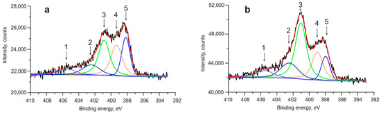
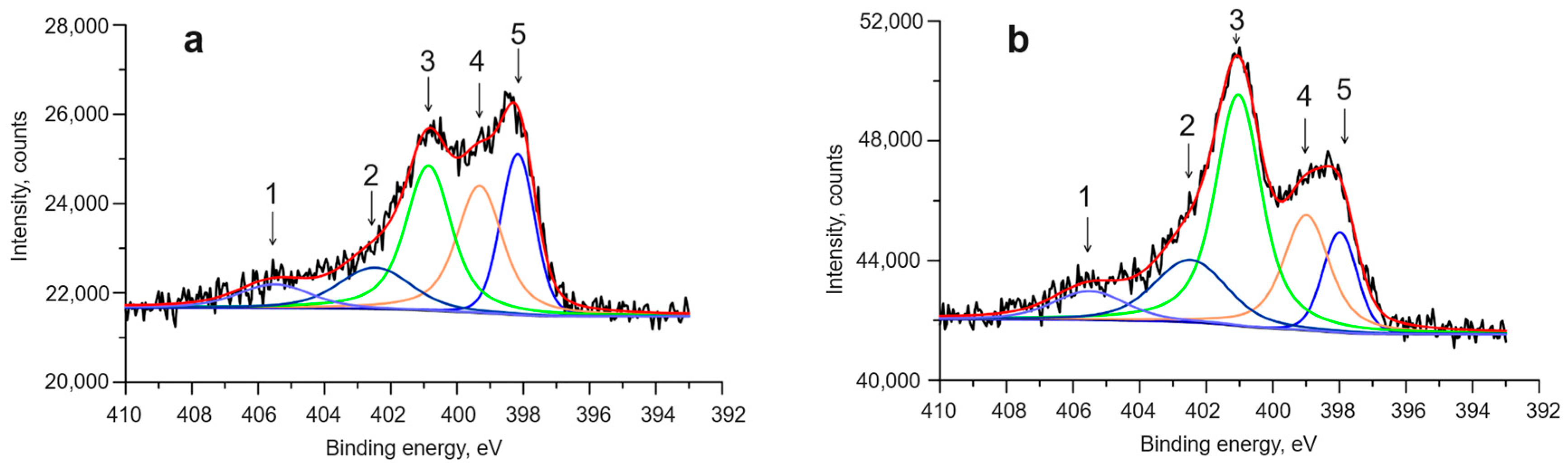
The incorporation of nitrogen into the VMWCNT structure is confirmed by XPS data (Figure 7). The obtained spectrum is deconvoluted into five components, pyridine N (~398.5 eV), pyrrole N (~400 eV), graphite-like N (~401 eV), NOx groups (~404 eV), and encapsulated molecular N2 (~405 eV), which is consistent with the systematic review data by [30], which compiled XPS results for various types of CNT. Let us note that the component at approximately 405 eV corresponds to molecular nitrogen that is mechanically encapsulated inside of the closed inner walls of the nanotubes and, possibly, in interlayer voids. The ability of MWCNT to encapsulate N2 is a well-established assignment for CVD- and PECVD-grown N-doped MWCNTs and was earlier demonstrated in [32,33,34,35].
Figure 7.
N1 s XPS spectra of VMWCNT synthesized at 550 °C (a) and 750 °C (b) (synthesis time 5 min; plasma mode PRF = 20 W, PLF = 30 W; working pressure 3 Torr). The spectral peaks correspond to the following arrangements: 1—pyridine-like, 2—pyrrole-like, 3—graphite-like, 4—with an NOx radical, 5—encapsulated molecular nitrogen.
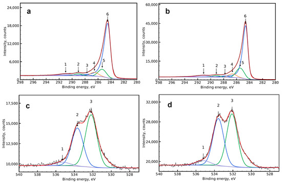
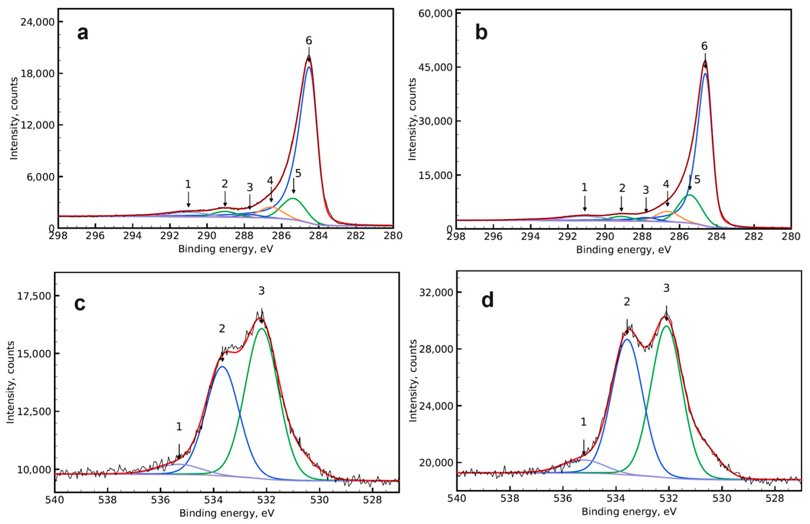
The C1 s and O1 s spectra (Figure 8) of the samples treated at 550 °C and 750 °C indicate the predominantly graphitic nature of the carbon component at both synthesis temperatures and the presence of oxygen-containing surface states. A model comprising six C1 s components and three O1 s components was used to fit the experimental spectra. Because nitrogen is present in the samples (see N1 s spectra), a number of the C1 s components include an unresolved contributions from C–N states.
Figure 8.
C1 s and O1 s XPS spectra of VMWCNT synthesized at 550 °C (a,c) and 750 °C (b,d) (synthesis time 5 min; plasma mode PRF = 20 W, PLF = 30 W; working pressure 3 Torr). The spectral C1 s peaks correspond to the following arrangements: 1—π→π*, 2—O–C=O, 3—C=O, O–C–O, 4—C–O–C, C–OH, C–N, 5—sp3-hybridized carbon, 6—sp2-hybridized carbon, for O1 s, respectively, 1—H2O, 2—O–C, 3—O=C.
The C1 s spectra are dominated by an asymmetric line at 284.5 and 284.6 eV, corresponding to sp2-hybridized carbon in graphitic walls; its position aligns with the 284.3–284.6 eV range established for graphitic materials. Components at 285.5 eV (line 5) represent a defective/disordered environment and may be equated with sp3-carbon content. Components at 286.2 are assigned to carbon bonded to a single oxygen atom (C–O–C, C–OH) with a possible C–N contribution; those at 287.2 to C=O/O–C–O states, with a possible contribution from amide N–C=O; and the component at 289.0 eV to the O–C=O region (carboxyl, ester, and related groups). A broad feature at 291 eV corresponds to the π→π* satellite characteristic of conjugated graphitic rings. This scheme follows the six-component model used for MWCNTs [36,37], although distinguishing between oxygen and nitrogen contributions within a single C1 s line is ambiguous. The area fractions of the C1 s components are sp2—72% and 66%; ~285.5 eV—6% and 9%; ~286.1 eV—7% and 9%; ~287.1 eV—5% and 6%; and ~289.0 eV—2% and 2%. The π→π* satellite accounts for 7% and 7%. These percentages are normalized to the total area of the components within the measured window (including the satellite) and do not represent the atomic fractions of the chemical groups.
In the O1 s spectra, the main components are located at 532.2 and 532.1 eV, as well as 533.6 eV. The third is attributed to double-bonded oxygen (carbonyl and carboxyl groups), and the second to single-bonded oxygen (hydroxyl, ether, and related groups). Literature values for graphite oxides and CNT cite ranges of 531.3–532.0 eV and 533.1–533.5 eV, respectively [38,39]; thus, the observed positions lie at the upper limit of, or slightly above, these intervals. High-energy contributions at 535.5 and 534.9 eV are traditionally associated with adsorbed water [38]; however, energy losses and asymmetry of the main lines are also possible in this region, so this assignment should be considered tentative. The O1 s area fractions are ~532.1 eV—49% and 43%; ~533.6 eV—40% and 44%; and ~535 eV—6% and 6%. The results are consistent with the preservation of the sp2-carbon framework at both synthesis temperatures and with the presence of both single- and double-bonded oxygen-containing surface states.
Based on the data in Figure 5, we suggest that the nanoparticles’ size, and, consequently, the diameter of the growing CNT, is determined primarily by the parameters of the catalyst pretreatments that form the nanoparticles [13]. Raising the synthesis temperature does not lead to a significant change in the size of the catalytic particles, as, by the time synthesis begins, identical pretreatment processes have already set the distribution of nanoparticles across the substrate surface; but, the temperature accelerates the growth process by increasing particle activity and, in conjunction with the action of the plasma, accelerates the formation of nanotube walls.
A temperature of 600 °C was selected as optimal based on two criteria: the quality of the resulting CNT array and compatibility with standard microelectronics processes. At this temperature, the CNT grow at a relatively high rate while retaining sufficient graphitic quality. Moreover, 600 °C lies below the ~660 °C melting point of the aluminum metallization used in CMOS processes, which is essential for CNT integration at later (BEOL) stages of chip fabrication.
3.2. The Effect of Synthesis Duration on VMWCNT Growth
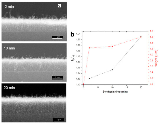
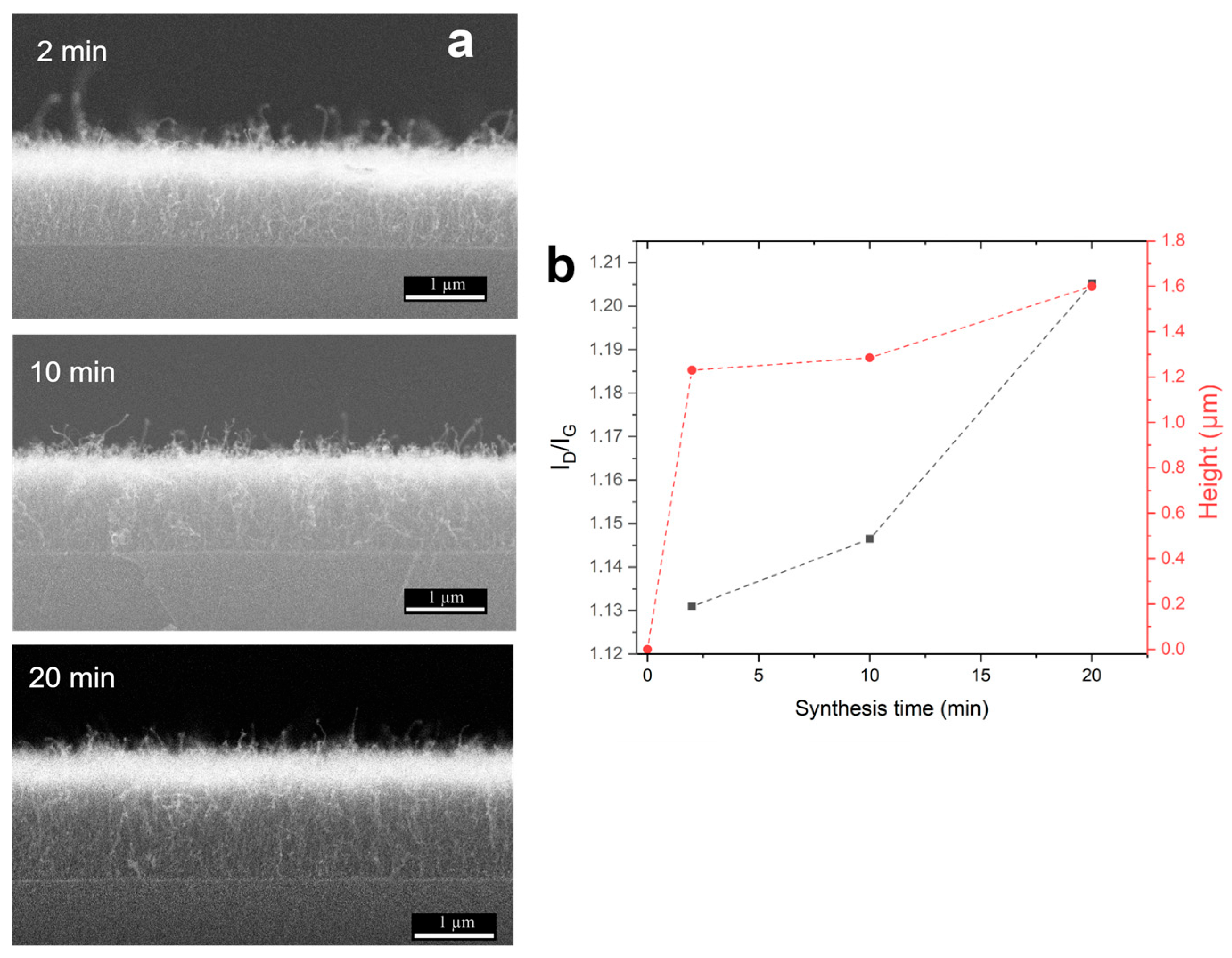
To experimentally investigate the effect of synthesis duration, experiments were conducted with times ranging from 2 to 20 min. Figure 9 shows SEM images of the synthesized arrays.
Figure 9.
SEM images of VMWCNT arrays synthesized over different synthesis durations (a) and a comparison of defect densities (b) (synthesis temperature 600 °C; plasma mode PRF = 20 W, PLF = 30 W; working pressure 3 Torr).
We have experimentally determined that a longer synthesis duration does not lead to a significant increase in the height of the nanotube arrays. This may be due to the fact that after a certain period of time, the catalyst material is consumed due to the periodic disintegration of the particle along the length of the CNT during nanotube growth; the mechanism of nanoparticle evolution and disintegration was investigated in [28]. At the same time, the growth mechanism described in the article results in bamboo-like CNT, and changes in the process parameters have little effect on the internal morphology of the nanotubes. Next, when the particle becomes sufficiently small or stretched and immobilized in the CNT channel, carbon deposited from the atmosphere completely covers it with an amorphous layer, which makes further growth of the carbon nanotube impossible.
Furthermore, increasing the synthesis time has no significant effect on the overall defect density of the MWCNT. At 600 °C, increasing the synthesis time from 2 to 20 min changed ID/IG by less than 6% and produced no detectable shift of the G band. We also note the characteristic presence of spectral contributions from modes at ~1200 cm−1 (the left shoulder of the D mode) and 1500 cm−1, associated with the inclusion of sp3 carbon and amorphous carbon, which is consistent with previously reported data for this temperature. We assume that the duration of synthesis should be selected based on the technical and technological characteristics of the substrates or microelectronic components used, as significant growth in height for the VMWCNT array occurs in the first couple of minutes and does not subsequently introduce significant changes in the final characteristics of the array. Additional experimental studies (not presented here) have shown that the main growth of the arrays occurs during the first minute, after which the growth rate of the VMWCNT decreases sharply.
3.3. The Effect of Plasma Power on VMWCNT Growth
The primary characteristic and most critical parameter of the synthesis process is the power and type of plasma used.
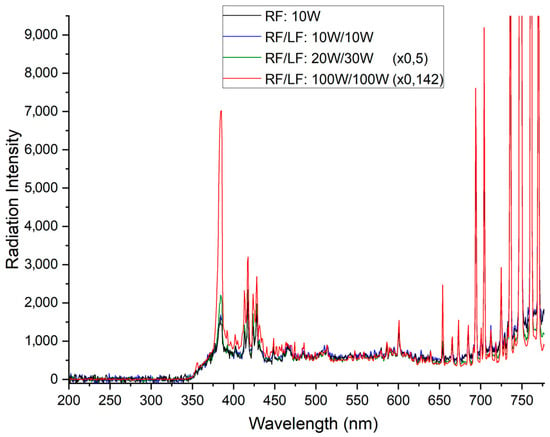
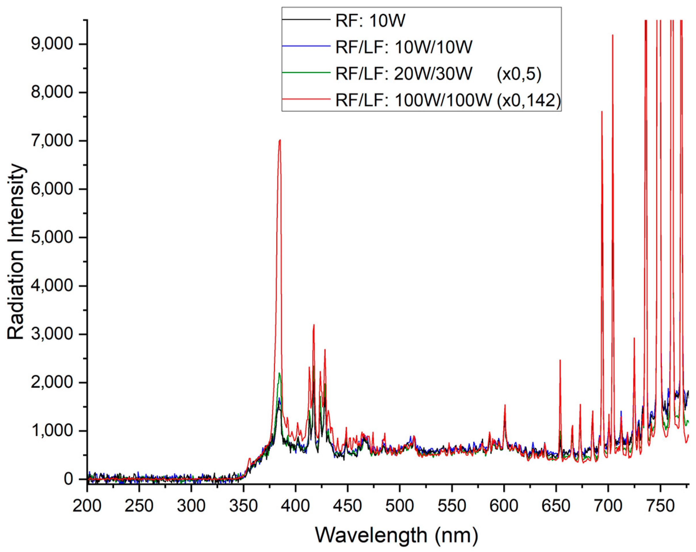
Plasma has a dual effect on MWCNT during growth, stimulating the decomposition of hydrocarbons while simultaneously etching protruding parts of the array, individual tubes, and solid carbon compounds, including amorphous ones, formed during CNT growth on the catalyst. The use of plasma-enhanced chemical vapor deposition also allows for improving the efficiency of MWCNT synthesis at low temperatures by transferring additional energy to the catalyst particles and increasing the rate of carbon diffusion into them [40]. An important challenge is finding a balance between the rate of growth as power increases and the etching process of the forming MWCNT when the threshold power is exceeded. It has been noted [41,42] that the use of high-power plasma in the synthesis of nanotubes not only increases their growth rate but also improves the orientation of the arrays. The optical emission plasma spectra we obtained during synthesis (Figure 10) at minimum and maximum powers (10 W RF and 100 W RF + LF) coincide at all peaks. An increase in power (from 10 W to 100/100 W) only enhances the absolute intensity of the emission (the spectra had to be scaled by factors of ×0.5 and ×0.142 for clarity) but does not alter the qualitative composition of the plasma; the set of excited particles and the ratio of the main lines remain unchanged. Thus, increasing the plasma power does not lead to a change in the nature of the effect but only to its intensification, both in terms of hydrocarbon decomposition and increased catalyst activity, as well as etching of the side walls of the growing VMWCNT.
Figure 10.
Plasma spectra during VMWCNT synthesis obtained with a power of 10 W RF, 10 W RF + 10 W LF, 20 W RF + 30 W LF, and 100 W RF + 100 W LF.
Currently, the following approaches exist to explain the mechanisms by which ion bombardment affects the growth of MWCNT when plasma is used:
- Ion bombardment can introduce defects (interstitial and substitutional atoms) into the structure of nanotubes, leading to distortions and deviations from the average diameter, as well as the amorphization of the MWCNT walls due to etching (caused by the large number of free radicals present in the plasma) [12,43,44].
- For the tip growth mechanism, it is assumed that the catalytic particles at the tip of the growing nanotube protect the tube from harmful ion bombardment (as the electric field intensifies at the tip of the growing structure, plasma ions will primarily act on the tip, thereby reducing the lateral mechanical stress on the tube) [45]; as for the growth mechanism at the base, it is assumed that the catalyst adheres to the substrate and the growing tubes are continuously subjected to ion bombardment [46].
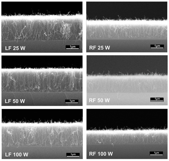
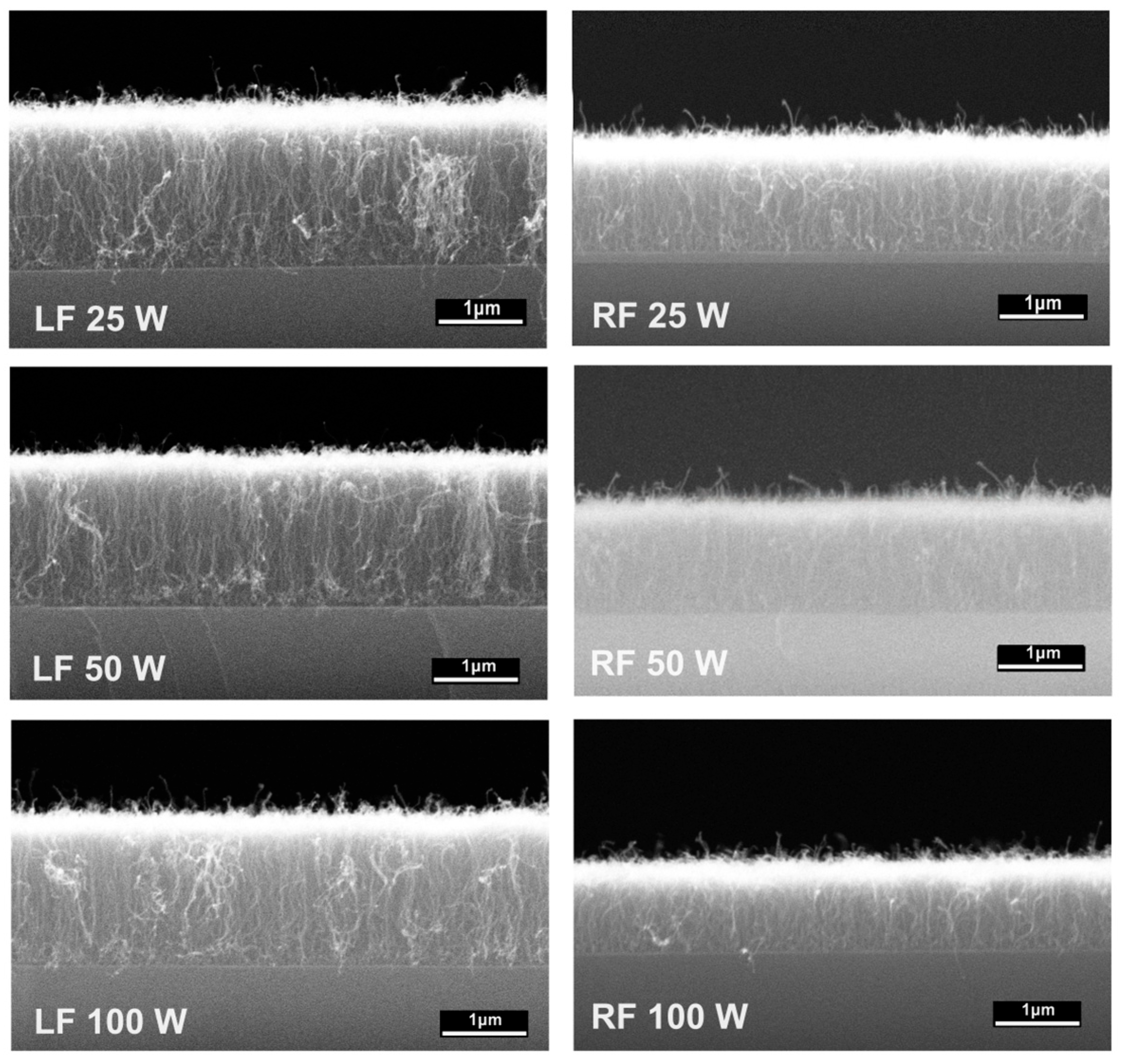
For our study, a set of experimental samples was prepared using RF and LF plasma of varying power levels. The following parameters were selected: for LF, frequency 450 kHz, power 25 W, 50 W, and 100 W; for RF, 13.56 MHz, power 25 W, 50 W, and 100 W. The synthesis time was uniformly set at 5 min. Figure 11 shows SEM images of the formed arrays.
Figure 11.
SEM images of VMWCNT arrays formed at various plasma power and frequency values (synthesis temperature 600 °C; synthesis time 5 min; working pressure 3 Torr).
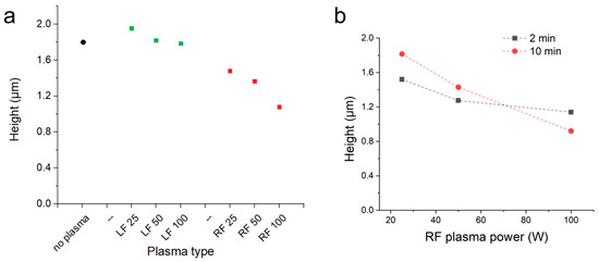
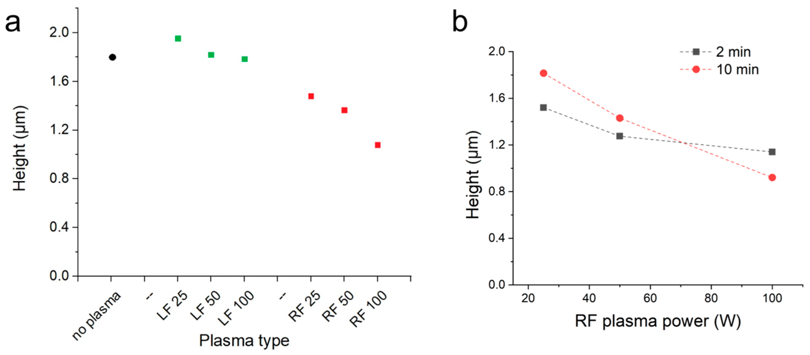
Based on the experimental data obtained, relationships between the height of the VMWCNT arrays and plasma power were plotted for both high-frequency and low-frequency exposure cases, as shown in Figure 12. The technological parameters of the pretreatment and synthesis processes are summarized in Table 1.
Figure 12.
The dependence of the height of the CNT arrays on plasma power for low-frequency and high-frequency irradiation (synthesis time 5 min; synthesis temperature 600 °C; working pressure 3 Torr) (a) and the effect of synthesis duration at different high-frequency plasma powers (b).
In both cases, it was found that increasing the plasma power leads to a gradual decrease in the height of the array due to its etching [47,48] and that the plasma primarily affects the overall appearance of the array and the structure and disorder of its upper part, including the number and type of rare protruding nanotubes. At the same time, changing the synthesis duration affects the height of the array at any plasma power, as demonstrated in studies conducted at different process durations of 2, 5, and 10 min.
3.4. The Effect of Operating Pressure and Gas Concentration on VMWCNT Growth
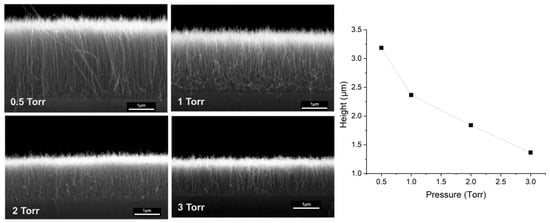
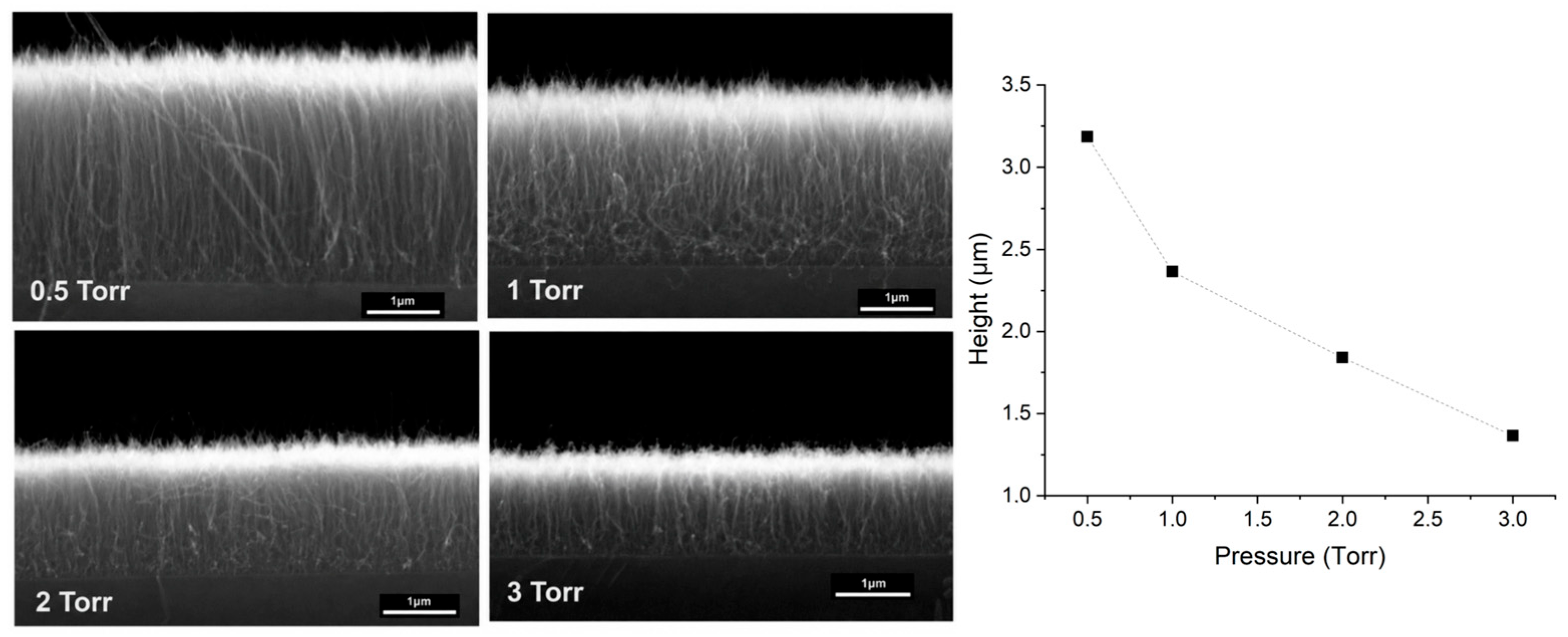
On the one hand, increasing the operating pressure in the reaction chamber during the synthesis process should lead to an increase in the growth rate of the nanotubes, as this raises the concentration of carbon particles. On the other hand, as pressure rises, the free path length of charged particles and radicals diminishes, which will reduce the effectiveness of the plasma’s influence on MWCNT growth. An experimental study on the effect of pressure in the reaction chamber during the synthesis process was carried out in the range of 0.5 to 3 Torr, determined by the chamber’s pumping rate. SEM images of the formed VMWCNT arrays are shown in Figure 13.
Figure 13.
SEM images of VMWCNT arrays after the synthesis process carried out at various pressures in the reaction chamber (synthesis time 5 min; synthesis temperature 600 °C; plasma mode PRF = 20 W, PLF = 30 W) and height tendency.
The results of the studies revealed an inverse linear relationship between the height of the VMWCNT array and the pressure in the reaction chamber. The maximum height was determined for arrays synthesized at a reaction chamber pressure of 0.5 Torr and amounted to 3.2 μm. At a pressure of 3 Torr, the height of the synthesized arrays was 2.5 times smaller at 1.4 μm. A similar trend was observed for CNT synthesized through the CVD method [49]. As suggested in [49], low pressure reduces the gas phase decomposition of the precursor (C2H2), thereby limiting the deposition of amorphous carbon (encapsulation of catalyst particles) and extending the effective lifetime of the catalyst.
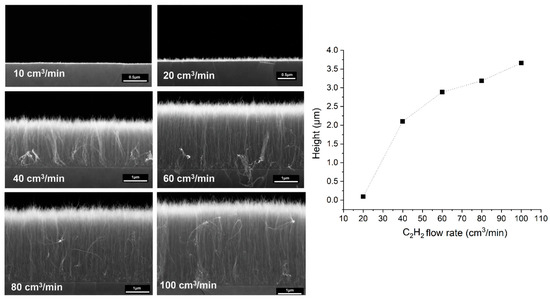
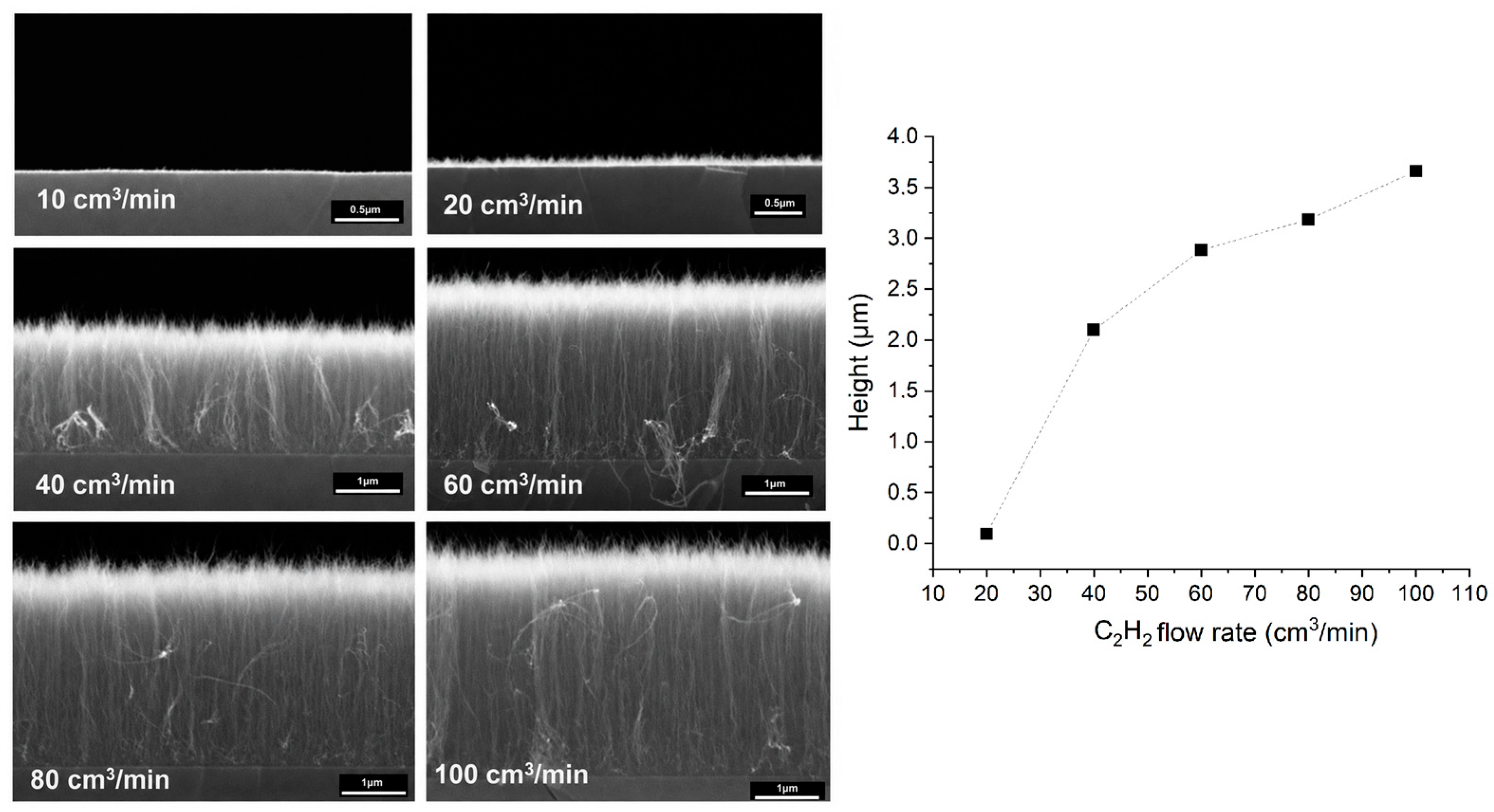
To investigate the effect of hydrocarbon gas concentration on the synthesis process, a set of experimental samples was prepared, for which VMWCNT synthesis was carried out under previously determined optimal synthesis conditions of NH3 flow rate = 100 cm3/min, 600 °C, PRF:PLF = 20 W:30 W, 5 min, and 0.5 Torr but at different hydrocarbon flow rates ranging from 10 to 100 cm3/min right up to the technologically feasible limit. SEM images of the synthesized VMWCNT arrays are shown in Figure 14.
Figure 14.
SEM images of VMWCNT arrays formed at various hydrocarbon flow rates (synthesis time 5 min; synthesis temperature 600 °C; plasma mode PRF = 20 W, PLF = 30 W; working pressure 0.5 Torr) and height tendency.
In the other experiments described in this article, the C2H2 flow rate was set to 100 cm3/min to ensure that a small amount of carbon would not limit the growth rate of the VMWCNT. For the same reasons, a chamber pressure of 3 Torr was initially selected, which, as it turned out, had a negative effect on the height of the array.
It was also experimentally shown that within the investigated range, as the hydrocarbon flow rate decreases, the height of the synthesized VMWCNT arrays decreases until synthesis ceases entirely.
4. Discussion
PECVD is a promising method for synthesizing MWCNT due to its ability to create vertically aligned structures at relatively low temperatures. Optimizing the synthesis parameters requires a careful balance between synthesis temperature and duration, plasma power, catalyst thickness, and gas composition. Varying these parameters allows us to control the dimensional and structural characteristics of nanotubes for various applications. Potentially important application areas include cold cathodes for field emission, which are crucial for electron microscope columns, vacuum microwave generators and amplifiers, and micro-X-ray devices. Currently, existing field emission cathodes suffer from low current density and short operational lifetimes. Research efforts are focused on developing cathodes characterized by long lifetimes, high stability, and resistance to heat, high voltages, and mechanical stress; in this context, CNTs emerge as one of the most promising candidates [50]. Beyond this area, CNT applications are also being developed for black coatings with unmatched efficiency [51,52] and for multifunctional biomedical components [53,54].
The growth of carbon nanotubes during the PECVD process can occur via two main mechanisms [55]. Traditionally, the VLS (vapor–liquid–solid) mechanism is considered, in which the catalyst is in a liquid state and carbon diffuses through the particle volume. However, at the relatively low temperatures of PECVD, the VSS (vapor–solid–solid) model is more relevant, where carbon diffusion occurs along the surface of the solid catalyst particles [56,57]. Depending on the interaction between the catalyst and the substrate, different mechanisms occur: in the case of weak interaction, tip growth takes place, in which the catalyst particle is located at the tip of the growing nanotube [28]; with strong interaction, base growth is observed, where the catalyst remains attached to the substrate [55]. If base growth occurs (the catalyst is attached to the substrate), the vertical alignment of the dense array of CNT is due to collective van der Waals interactions (the crowding effect), as demonstrated in [58]. The authors note that the heterogeneous stress (tensile and compressive) at the interface between the catalyst particle and the carbon fiber creates conditions for the stabilization of growth in the vertical direction; however, any initial deviation from the vertical direction will be exponentially amplified, leading to chaotic growth in random orientations.
In addition, a number of studies have shown that the activation energy for the growth of VMWCNT during PECVD synthesis lies in the range of approximately 0.2–1 eV (e.g., 0.56 eV for vertically aligned tubular MWCNT with 20–30 walls [59], 0.76 eV for PECVD and 1.21 eV for thermal CVD in [60], 0.23 eV for vertically aligned bamboo-type CNT via PECVD [61], and 0.23–0.35 eV for Ni, Co, and Fe catalysts in [62]), which corresponds to the surface diffusion of carbon across nickel (0.3 eV). This confirms that the rate-limiting step is the surface diffusion of carbon atoms on the catalyst particle (for thermal CVD, the activation energy of the C–N bond is higher, and thus the assigned growth-rate-limiting process is bulk diffusion of carbon through the solid catalyst particle) [55].
In the course of our research, and by synthesizing the findings of scientific studies in related fields, we have established the following:
- (1)
- Temperature is a critical parameter that determines both the growth rate and the quality of the resulting nanotubes. As the temperature increases from 500 to 800 °C, the height of the array increases, and the alignment and density of the nanotubes improve. According to Raman spectroscopy data, the best graphitic quality (minimum ID/IG, narrow and intense 2D band, absence of contributions from bands near 1200 and 1500 cm−1) is achieved at 750–800 °C, while at 500 °C the proportion of amorphous and sp3 carbon increases significantly; from the perspective of integration with microelectronic materials, a temperature of approximately 600 °C proves to be technologically optimal, ensuring acceptable growth without degradation of the metallization.
- (2)
- Extending the synthesis duration has a much smaller effect: the main growth in height occurs in the first few minutes, after which the growth rate drops sharply. Extending the duration has virtually no effect on defect density (the ID/IG ratio changes by approximately 6%); therefore, it is advisable to select the duration based on the thermal limit permissible for the specific substrate.
- (3)
- Plasma and ion bombardment play a dual role: increasing plasma power (both high-frequency and low-frequency) improves the orientation and alignment of the arrays by intensifying growth but at the same time increases wall etching, which leads to a reduction in height.
- (4)
- In the studied range of 0.5–3 Torr, the height of the VMWCNT is inversely related to the pressure in the chamber. The maximum height is reached at 0.5 Torr, which is explained by the minimization of the encapsulation of catalyst particles by amorphous carbon due to a decrease in the precursor amount.
- (5)
- The flow rate of the hydrocarbon component determines whether the supply of activated carbon is the rate-limiting step: at fixed optimal temperatures, plasma power, and pressure, a decrease in the hydrocarbon flow rate leads to a reduction in the height of the arrays, up to the point where growth is completely suppressed. Increasing the hydrocarbon concentration in the total gas mixture within the range studied in this article allows for increasing the height of the synthesized VMWCNT.
During growth, plasma exposure stimulates synthesis by generating ions and radicals in the gas phase, removes amorphous carbon from the catalyst surface, and transfers additional energy to the catalyst. Once the active growth phase ends, the plasma’s influence is limited to Ar etching of the CNT and the formation of C–H and C–N species. In this case, both types of plasma gradually reduce the height of the VMWCNT as the power and duration of the process increase.
By simultaneously varying the temperature, synthesis time, plasma power and frequency, pressure, and gas flow rates, it is possible to precisely control the height, diameter, uniformity, and degree of graphitization of the MWCNT for applications in micro- and nanoelectronics. The main factors influencing the growth kinetics of nanotubes are temperature, pressure, and the flow rate of the precursor gas. The differences in the parameters of the arrays obtained during synthesis with different types of plasma are most likely determined by the varying effects on the nanotube walls and, in general, on the quality of the graphite surface, including the alignment of the array due to reactive ion effects on the catalyst particles, which requires further analysis.
5. Conclusions
Our research shows that despite the large number of variable process parameters and their obvious influence on the growth of carbon nanotubes, the main morphological characteristics of the array remain unchanged. The properties of the formed multi-walled carbon nanotubes, including their average diameter, array height, and defect density, can be controlled. The presence of plasma allows for selectively removing CNT with abnormal lengths and ensures finer control over the array height. At the same time, the catalyst, which is located at the top of the growing nanotube and defines its growth through short cycles of nanoparticle lifting along the nanotube channel, determines the specific features of the nanotube’s internal structure, including bamboo-like walls and periodic changes in the direction of growth.
This paper experimentally analyzed the effect of key process parameters on the characteristics of the resulting arrays of multi-walled carbon nanotubes. Apart from temperature, an increase in which leads to both improved nanotube quality and higher array height, the contribution of synthesis duration was evaluated under simultaneous exposure to high- and low-frequency plasma of varying power. The resulting nonlinear dependence of the growth rate on time indicates that under these PECVD conditions, the catalyst nanoparticles utilize their full potential within the first few minutes of the process. During growth, plasma exposure stimulates synthesis by generating ions and radicals in the gas phase, removes amorphous carbon from the catalyst surface, and transfers additional energy to the catalyst. Once the active growth phase ends, the plasma’s influence is limited to Ar etching of the CNT and the formation of C–H and C–N species. In this case, both types of plasma gradually reduce the height of the VMWCNT as the power and duration of the process increase.
Temperature has a significant effect on the types of defects present in CNT. Nitrogen embedded in CNT is initially found in high concentrations in less thermodynamically stable positions, the pyrrole and pyridine sites. As the temperature rises, the concentration of nitrogen in the nanotubes decreases slightly, but there is a significant increase in nitrogen in the more thermodynamically favorable N-graphite-like form, which preserves the structural integrity of the nanotube walls. This further enhances the quality of the CNT, as shown by the results of Raman spectroscopy.
An increase in chamber pressure leads to a decline in VMWCNT height, which appears to be associated with a lower rate of gas renewal, resulting in a carbon deficit in the synthesis site. Within the studied range of acetylene flow rates, a barely noticeable increase in the array rapidly transforms into intense synthesis as the flow rate rises.
The obtained correlations between VMWCNT growth and synthesis parameters could be useful in industrial applications requiring a maximum or controlled array height and stability under harsh conditions—for example, for field emission cathodes.
Author Contributions
Conceptualization, E.P.K.; methodology, A.A.S.; validation, E.P.K.; formal analysis, Y.O.V. and A.A.S.; investigation, Y.O.V., A.A.S., R.M.R., P.A.E., L.S.V. and P.N.V.; resources, V.V.S.; data curation, E.P.K. and Y.O.V.; writing—original draft preparation, E.P.K., Y.O.V. and R.M.R.; writing—review and editing, V.V.S.; visualization, Y.O.V.; supervision, V.V.S.; project administration, E.P.K. All authors have read and agreed to the published version of the manuscript.
Funding
This study was supported by the Ministry of Science and Higher Education of the Russian Federation as part of the government task [project No. FNRM-2024-0001].
Data Availability Statement
The raw data required to reproduce these findings are available upon request by email to the corresponding author: kitsyuk.e@gmail.com.
Acknowledgments
The authors would like to thank R. Chumakov for the XPS analysis. We thank E. Ambrochi for help with the illustrations.
Conflicts of Interest
The authors declare no conflicts of interest. The funders had no role in the design of the study; in the collection, analyses, or interpretation of data; in the writing of the manuscript; or in the decision to publish the results.
Abbreviations
The following abbreviations are used in this manuscript:
| CNT | Carbon nanotubes |
| CVD | Chemical vapor deposition |
| LF | Low-frequency plasma power |
| MWCNT | Multi-walled carbon nanotubes |
| PECVD | Plasma-enhanced chemical vapor deposition |
| RF | High-frequency plasma power |
| SEM | Scanning electron microscopy |
| TEM | Transmission electron microscopy |
| VACNT | Vertically aligned carbon nanotubes |
| VMWCNT | Vertical array of multi-walled carbon nanotubes |
| XPS | X-ray photoelectron spectroscopy |
References
- Ando, Y. Carbon Nanotube: The Inside Story. J. Nanosci. Nanotechnol. 2010, 10, 3726–3738. [Google Scholar] [CrossRef] [Scilit] [PubMed]
- Lehman, J.H.; Terrones, M.; Mansfield, E.; Hurst, K.E.; Meunier, V. Evaluating the Characteristics of Multiwall Carbon Nanotubes. Carbon 2011, 49, 2581–2602. [Google Scholar] [CrossRef] [Scilit]
- Bokobza, L. Multiwall Carbon Nanotube Elastomeric Composites: A Review. Polymer 2007, 48, 4907–4920. [Google Scholar] [CrossRef] [Scilit]
- Milne, W.I.; Teo, K.B.K.; Amaratunga, G.A.J.; Legagneux, P.; Gangloff, L.; Schnell, J.-P.; Semet, V.; Binh, V.T.; Groening, O. Carbon Nanotubes as Field Emission Sources. J. Mater. Chem. 2004, 14, 933–943. [Google Scholar] [CrossRef] [Scilit]
- Tong, T.; Zhao, Y.; Delzeit, L.; Kashani, A.; Meyyappan, M.; Majumdar, A. Dense Vertically Aligned Multiwalled Carbon Nanotube Arrays as Thermal Interface Materials. IEEE Trans. Compon. Packag. Technol. 2007, 30, 92–100. [Google Scholar] [CrossRef] [Scilit]
- Kiamahalleh, M.V.; Zein, S.H.S.; Najafpour, G.; Sata, S.A.; Buniran, S. Multiwalled Carbon Nanotubes Based Nanocomposites for Supercapacitors: A Review of Electrode Materials. Nano 2012, 7, 1230002. [Google Scholar] [CrossRef] [Scilit]
- Schroeder, V.; Savagatrup, S.; He, M.; Lin, S.; Swager, T.M. Carbon Nanotube Chemical Sensors. Chem. Rev. 2018, 119, 599–663. [Google Scholar] [CrossRef] [Scilit] [PubMed]
- Peng, L.M.; Zhang, Z.; Qiu, C. Carbon Nanotube Digital Electronics. Nat. Electron. 2019, 2, 499–505. [Google Scholar] [CrossRef] [Scilit]
- Su, Y.; Zhang, Y. Carbon Nanomaterials Synthesized by Arc Discharge Hot Plasma. Carbon 2015, 83, 90–99. [Google Scholar] [CrossRef] [Scilit]
- Arepalli, S. Laser Ablation Process for Single-Walled Carbon Nanotube Production. J. Nanosci. Nanotechnol. 2004, 4, 317–325. [Google Scholar] [CrossRef] [Scilit] [PubMed]
- Terranova, M.L.; Sessa, V.; Rossi, M. The World of Carbon Nanotubes: An Overview of CVD Growth Methodologies. Chem. Vap. Depos. 2006, 12, 315–325. [Google Scholar] [CrossRef] [Scilit]
- Meyyappan, M.; Delzeit, L.; Cassell, A.; Hash, D. Carbon Nanotube Growth by PECVD: A Review. Plasma Sources Sci. Technol. 2003, 12, 205. [Google Scholar] [CrossRef] [Scilit]
- Kitsyuk, E.P.; Vasilevskaya, Y.O.; Volovlikova, O.V.; Eganova, E.M.; Dudin, A.A. Catalytic Particles Formation from Thin Nickel Films for the Synthesis of Multi-Walled Carbon Nanotubes. Carbon 2024, 229, 119509. [Google Scholar] [CrossRef] [Scilit]
- Brown, S.D.M.; Jorio, A.; Dresselhaus, M.S.; Dresselhaus, G. Observations of the D-Band Feature in the Raman Spectra of Carbon Nanotubes. Phys. Rev. B 2001, 64, 073403. [Google Scholar] [CrossRef] [Scilit]
- Dresselhaus, M.S.; Jorio, A.; Filho, A.G.S.; Saito, R. Defect Characterization in Graphene and Carbon Nanotubes Using Raman Spectroscopy. Philos. Trans. R. Soc. A 2010, 368, 5355–5377. [Google Scholar] [CrossRef] [Scilit] [PubMed]
- Dresselhaus, M.S.; Dresselhaus, G.; Saito, R.; Jorio, A. Raman Spectroscopy of Carbon Nanotubes. Phys. Rep. 2005, 409, 47–99. [Google Scholar] [CrossRef] [Scilit]
- Venezuela, P.; Lazzeri, M.; Mauri, F. Theory of Double-Resonant Raman Spectra in Graphene: Intensity and Line Shape of Defect-Induced and Two-Phonon Bands. Phys. Rev. B 2011, 84, 035433. [Google Scholar] [CrossRef] [Scilit]
- Gouadec, G.; Colomban, P. Raman Spectroscopy of Nanomaterials: How Spectra Relate to Disorder, Particle Size and Mechanical Properties. Prog. Cryst. Growth Charact. Mater. 2007, 53, 1–56. [Google Scholar] [CrossRef] [Scilit]
- Jorio, A.; Saito, R. Raman Spectroscopy for Carbon Nanotube Applications. J. Appl. Phys. 2021, 129, 021102. [Google Scholar] [CrossRef] [Scilit]
- Eckmann, A.; Felten, A.; Mishchenko, A.; Britnell, L.; Krupke, R.; Novoselov, K.S.; Casiraghi, C. Probing the Nature of Defects in Graphene by Raman Spectroscopy. Nano Lett. 2012, 12, 3925–3930. [Google Scholar] [CrossRef] [Scilit] [PubMed]
- Hu, Y.; Guo, C. Carbon Nanotubes and Carbon Nanotubes/Metal Oxide Heterostructures: Synthesis, Characterization and Electrochemical Property. In Carbon Nanotubes—Growth and Applications; IntechOpen: Rijeka, Croatia, 2011. [Google Scholar] [CrossRef] [Scilit] [PubMed]
- Xu, N.; Tsang, S.H.; Tay, B.K.; Teo, E.H.T.; Ng, C.M. Growth of Carbon Nanotubes on Carbon/Cobalt Films with Different sp2/sp3 Ratios. J. Nanomater. 2013, 2013, 730952. [Google Scholar] [CrossRef] [Scilit]
- Ferrari, A.C.; Basko, D.M. Raman Spectroscopy as a Versatile Tool for Studying the Properties of Graphene. Nat. Nanotechnol. 2013, 8, 235–246. [Google Scholar] [CrossRef] [Scilit] [PubMed]
- Puech, P.; Kandara, M.; Paredes, G.; Moulin, L.; Weiss-Hortala, E.; Kundu, A.; Ratel-Ramond, N.; Plewa, J.-M.; Pellenq, R.; Monthioux, M. Analyzing the Raman Spectra of Graphenic Carbon Materials from Kerogens to Nanotubes: What Type of Information Can Be Extracted from Defect Bands? C 2019, 5, 69. [Google Scholar] [CrossRef] [Scilit]
- Sadezky, A.; Muckenhuber, H.; Grothe, H.; Niessner, R.; Pöschl, U. Raman Microspectroscopy of Soot and Related Carbonaceous Materials: Spectral Analysis and Structural Information. Carbon 2005, 43, 1731–1742. [Google Scholar] [CrossRef] [Scilit]
- Düngen, P.; Prenzel, M.; Van Stappen, C.; Pfänder, N.; Heumann, S.; Schlögl, R. Investigation of Different Pre-Treated Multi-Walled Carbon Nanotubes by Raman Spectroscopy. Mater. Sci. Appl. 2017, 8, 628–641. [Google Scholar] [CrossRef]
- Bukunov, K.A.; Vorobyeva, E.A.; Chechenin, N.G. Features of Raman Light Scattering in Arrays of Vertically Aligned Multi-Walled Carbon Nanotubes. Mosc. Univ. Phys. Bull. 2022, 77, 50–56. [Google Scholar] [CrossRef] [Scilit]
- Lin, P.A.; Natarajan, B.; Zwolak, M.; Sharma, R. Metastable Morphological States of Catalytic Nanoparticles. Nanoscale 2018, 10, 4528–4537. [Google Scholar] [CrossRef] [Scilit] [PubMed]
- Arjmand, M.; Sadeghi, S. Nanocomposites Towards Thermoelectric Applications. In Thermoelectrics for Power Generation: A Look at Trends in the Technology; IntechOpen: Rijeka, Croatia, 2016; p. 323. [Google Scholar] [CrossRef] [Scilit] [PubMed]
- Susi, T.; Pichler, T.; Ayala, P. X-Ray Photoelectron Spectroscopy of Graphitic Carbon Nanomaterials Doped with Heteroatoms. Beilstein J. Nanotechnol. 2015, 6, 177–192. [Google Scholar] [CrossRef] [Scilit] [PubMed]
- Korusenko, P.M.; Bolotov, V.V.; Nesov, S.N.; Povoroznyuk, S.N.; Khailov, I.P. Changes of the Electronic Structure of the Atoms of Nitrogen in Nitrogen-Doped Multiwalled Carbon Nanotubes Under the Influence of Pulsed Ion Radiation. Nucl. Instrum. Methods Phys. Res. Sect. B 2015, 358, 131–135. [Google Scholar] [CrossRef] [Scilit]
- Choi, H.C.; Bae, S.Y.; Jang, W.-S.; Park, J.; Song, H.J.; Shin, H.-J.; Jung, H.; Ahn, J.-P. Release of N2 from the Carbon Nanotubes via High-Temperature Annealing. J. Phys. Chem. B 2005, 109, 1683–1688. [Google Scholar] [CrossRef] [Scilit] [PubMed]
- Choi, H.C.; Park, J.; Kim, B. Distribution and Structure of N Atoms in Multiwalled Carbon Nanotubes Using Variable-Energy X-ray Photoelectron Spectroscopy. J. Phys. Chem. B 2005, 109, 4333–4340. [Google Scholar] [CrossRef] [Scilit] [PubMed]
- Zhou, J.; Wang, J.; Liu, H.; Banis, M.N.; Sun, X.; Sham, T.-K. Imaging Nitrogen in Individual Carbon Nanotubes. J. Phys. Chem. Lett. 2010, 1, 1709–1713. [Google Scholar] [CrossRef] [Scilit]
- Kramberger, C.; Thurakitseree, T.; Einarsson, E.; Takashima, A.; Kinoshita, T.; Muro, T.; Maruyama, S. From Isotope Labeled CH3CN to N2 Inside Single-Walled Carbon Nanotubes. Nanoscale 2014, 6, 1525–1528. [Google Scholar] [CrossRef] [Scilit] [PubMed]
- Kwiatkowska, M.; Pełech, R.; Jędrzejewska, A.; Moszyński, D.; Pełech, I. Different Approaches to Oxygen Functionalization of Multi-Walled Carbon Nanotubes and Their Effect on Mechanical and Thermal Properties of Polyamide 12 Based Composites. Polymers 2020, 12, 308. [Google Scholar] [CrossRef] [Scilit] [PubMed]
- Gengenbach, T.R.; Major, G.H.; Linford, M.R.; Easton, C.D. Practical Guides for X-ray Photoelectron Spectroscopy (XPS): Interpreting the Carbon 1s Spectrum. J. Vac. Sci. Technol. A 2021, 39, 013204. [Google Scholar] [CrossRef] [Scilit]
- Mowbray, D.J.; Pérez Paz, A.; Ruiz-Soria, G.; Sauer, M.; Lacovig, P.; Dalmiglio, M.; Lizzit, S.; Yanagi, K.; Goldoni, A.; Pichler, T.; et al. Disentangling Vacancy Oxidation on Metallicity-Sorted Carbon Nanotubes. J. Phys. Chem. C 2016, 120, 18316–18322. [Google Scholar] [CrossRef] [Scilit]
- Easton, C.D.; Morgan, D.J. Critical Examination of the Use of X-ray Photoelectron Spectroscopy (XPS) O 1s to Characterize Oxygen Vacancies in Catalytic Materials and Beyond. J. Vac. Sci. Technol. A 2025, 43, 053205. [Google Scholar] [CrossRef] [Scilit]
- Hofmann, S.; Kleinsorge, B.; Ducati, C.; Robertson, J. Controlled Low-Temperature Growth of Carbon Nanofibres by Plasma Deposition. New J. Phys. 2003, 5, 153. [Google Scholar] [CrossRef] [Scilit]
- Das, D.; Roy, A. Synthesis of Diameter Controlled Multiwall Carbon Nanotubes by Microwave Plasma-CVD on Low-Temperature and Chemically Processed Fe Nanoparticle Catalysts. Appl. Surf. Sci. 2020, 515, 146043. [Google Scholar] [CrossRef] [Scilit]
- Liu, Y.; He, J.; Zhang, N.; Zhang, W.; Zhou, Y.; Huang, K. Advances of Microwave Plasma-Enhanced Chemical Vapor Deposition in Fabrication of Carbon Nanotubes: A Review. J. Mater. Sci. 2021, 56, 12559–12583. [Google Scholar] [CrossRef] [Scilit]
- Luo, Z.; Lim, S.; You, Y.; Miao, J.; Gong, H.; Zhang, J.; Wang, S.; Lin, J.; Shen, Z. Effect of Ion Bombardment on the Synthesis of Vertically Aligned Single-Walled Carbon Nanotubes by Plasma-Enhanced Chemical Vapor Deposition. Nanotechnology 2008, 19, 255607. [Google Scholar] [CrossRef] [Scilit] [PubMed]
- Eswara, S.; Audinot, J.N.; Adib, B.E.; Guennou, M.; Wirtz, T.; Philipp, P. Defect Formation in Multiwalled Carbon Nanotubes Under Low-Energy He and Ne Ion Irradiation. Beilstein J. Nanotechnol. 2018, 9, 1951–1963. [Google Scholar] [CrossRef] [Scilit] [PubMed]
- Neyts, E.C. The Role of Ions in Plasma Catalytic Carbon Nanotube Growth: A Review. Front. Chem. Sci. Eng. 2015, 9, 154–162. [Google Scholar] [CrossRef] [Scilit]
- Gohier, A.; Minea, T.M.; Djouadi, M.A.; Granier, A. Impact of the Etching Gas on Vertically Oriented Single Wall and Few Walled Carbon Nanotubes by Plasma Enhanced Chemical Vapor Deposition. J. Appl. Phys. 2007, 101, 054317. [Google Scholar] [CrossRef] [Scilit]
- Behr, M.J.; Gaulding, E.A.; Mkhoyan, K.A.; Aydil, E.S. Hydrogen Etching and Cutting of Multiwall Carbon Nanotubes. J. Vac. Sci. Technol. B 2010, 28, 1187–1194. [Google Scholar] [CrossRef] [Scilit][Green Version]
- Gohel, A.; Chin, K.; Zhu, Y.; Sow, C.; Wee, A. Field Emission Properties of N2 and Ar Plasma-Treated Multi-Wall Carbon Nanotubes. Carbon 2005, 43, 2530–2535. [Google Scholar] [CrossRef] [Scilit]
- Li, C.H.; Tseng, S.; Lo, S.; Chen, K.; Juang, Z.; Leou, K.; Tsai, C. Pressure Effect of Low-Temperature Growth of Multi-Wall Carbon Nanotubes on Nickel Catalyst/Barrier-Coated Glass by Thermal-CVD. Surf. Coat. Technol. 2006, 200, 3220–3223. [Google Scholar] [CrossRef] [Scilit]
- Li, J.; Tu, Y.; Ma, D.; Yang, Y. Research Progress in Carbon Nanotube-Based Cold Cathode Electron Guns. Nanomaterials 2025, 15, 1403. [Google Scholar] [CrossRef] [Scilit] [PubMed]
- Lehman, J.; Yung, C.; Tomlin, N.; Conklin, D.; Stephens, M. Carbon Nanotube-Based Black Coatings. Appl. Phys. Rev. 2018, 5, 011103. [Google Scholar] [CrossRef] [Scilit]
- Yang, P.; Liu, Y.; Wei, X.; Liu, Y.; Huang, S. Ultra-Black Materials: Fundamentals, Design, and Applications. Laser Photonics Rev. 2026, 20, e02136. [Google Scholar] [CrossRef] [Scilit]
- Kohls, A.; Ditty, M.M.; Dehghandehnavi, F.; Zheng, S.-Y. Vertically Aligned Carbon Nanotubes as a Unique Material for Biomedical Applications. ACS Appl. Mater. Interfaces 2022, 14, 6287–6306. [Google Scholar] [CrossRef] [Scilit] [PubMed]
- Komane, P.P.; Kumar, P.; Choonara, Y.E.; Pillay, V. Functionalized, Vertically Super-Aligned Multiwalled Carbon Nanotubes for Potential Biomedical Applications. Int. J. Mol. Sci. 2020, 21, 2276. [Google Scholar] [CrossRef] [Scilit] [PubMed]
- Kharlamova, M.V. Investigation of Growth Dynamics of Carbon Nanotubes. Beilstein J. Nanotechnol. 2017, 8, 826–856. [Google Scholar] [CrossRef] [Scilit] [PubMed]
- Sato, H.; Hata, K. Growth of Carbon Nanotubes by Plasma-Enhanced Chemical Vapor Deposition. New Diam. Front. Carbon Technol. 2006, 16, 163–176. [Google Scholar]
- Lim, S.; Luo, Z.; Shen, Z.; Lin, J. Plasma-Assisted Synthesis of Carbon Nanotubes. Nanoscale Res. Lett. 2010, 5, 1377. [Google Scholar] [CrossRef] [Scilit] [PubMed]
- Merkulov, V.I.; Melechko, A.V.; Guillorn, M.A.; Lowndes, D.H.; Simpson, M.L. Alignment Mechanism of Carbon Nanofibers Produced by Plasma-Enhanced Chemical-Vapor Deposition. Appl. Phys. Lett. 2001, 79, 2970–2972. [Google Scholar] [CrossRef] [Scilit]
- Chhowalla, M.; Teo, K.B.K.; Ducati, C.; Rupesinghe, N.L.; Amaratunga, G.A.J.; Ferrari, A.C.; Roy, D.; Robertson, J.; Milne, W.I. Growth Process Conditions of Vertically Aligned Carbon Nanotubes Using Plasma Enhanced Chemical Vapor Deposition. J. Appl. Phys. 2001, 90, 5308–5317. [Google Scholar] [CrossRef] [Scilit]
- Ducati, C.; Alexandrou, I.; Chhowalla, M.; Amaratunga, G.A.; Robertson, J. Temperature Selective Growth of Carbon Nanotubes by Chemical Vapor Deposition. J. Appl. Phys. 2002, 92, 3299–3303. [Google Scholar] [CrossRef] [Scilit]
- Hofmann, S.; Ducati, C.; Robertson, J.; Kleinsorge, B. Low-temperature growth of carbon nanotubes by plasma-enhanced chemical vapor deposition. Appl. Phys. Lett. 2003, 83, 135–137. [Google Scholar] [CrossRef] [Scilit]
- Hofmann, S.; Csanyi, G.; Ferrari, A.C.; Payne, M.C.; Robertson, J. Surface Diffusion: The Low Activation Energy Path for Nanotube Growth. Phys. Rev. Lett. 2005, 95, 036101. [Google Scholar] [CrossRef] [Scilit] [PubMed]

Disclaimer/Publisher’s Note: The statements, opinions and data contained in all publications are solely those of the individual author(s) and contributor(s) and not of MDPI and/or the editor(s). MDPI and/or the editor(s) disclaim responsibility for any injury to people or property resulting from any ideas, methods, instructions or products referred to in the content. |
© 2026 by the authors. Licensee MDPI, Basel, Switzerland. This article is an open access article distributed under the terms and conditions of the Creative Commons Attribution (CC BY) license.