


Abstract
High operating temperature mid-wavelength InAs/GaSb superlattice infrared photodetectors with a single heterojunction structure grown by metal–organic chemical vapor deposition are reported. By inserting a fully-depleted wider-gap barrier layer between the absorber and the p-contact, “diffusion-limited” behavior has been achieved for the heterojunction “PNn” device, in contrast to the conventional pin homojunction device. The PNn device with a 50% cutoff wavelength of 4.5 exhibited a dark current of 2.05 10−4 A/cm2 and a peak specific detectivity of 1.28 1011 at 150 K and a reverse bias of −0.1 V.
1. Introduction
Mid-wavelength infrared (MWIR) (3–5 m) detectors are desired for a variety of civilian and military applications such as industrial process monitoring, satellite reconnaissance, and night vision. One critical requirement of the MWIR detectors is the capability of high operating temperature (HOT) operation [1], which reduces the burden of cryogenic cooling significantly and leads to a reduction in size and total cost of the detector system [2]. After decades of development, Sb-based type-II superlattices (T2SLs) has proved to be a viable solution for a variety of infrared detection applications and been considered as a competitive candidate for the HOT MWIR detectors, due to their advantages of band gap tunability, flexibility of band structure engineering [3], large electron effective masses [4], and low Auger recombination [5].
The most important factor affecting the performance of the MWIR detectors at high operating temperature is the dark current, which increases dramatically as the temperature rises and leads to a high noise level. A new type of infrared detectors known as barrier detectors initially proposed by Maimon et al. [6] in 2006 have shown excellent performances in suppressing the generation–recombination (G-R) dark current. The T2SLs with their high design flexibility of band structure inject considerable vitality into the development of the barrier detectors and have motivated various heterostructures, such as the PMn structure [7,8], pMp structure [9], nBn structure [10,11], and pBn structure [12]. However, these structures are usually sophisticated and require a precise control of the thickness and composition. Moreover, these T2SL detectors are normally grown by molecular beam epitaxy (MBE). Although MBE technology can grow SL materials of high-quality, the high cost during mass production remains a crucial challenge.
In the III–V industry, the metal–organic chemical vapor deposition (MOCVD) is dominant in material growth because of its low-cost production and high throughput [13]. In 2011, Huang et al. have demonstrated MOCVD-grown InAs/GaSb based LWIR photodetectors on the InAs substrate, which shows a specific detectivity (D*) of about 6.78 109 at 8 at 78 K [14]. In 2019, Wu et al. reported MOCVD-grown InAs/InAsSb based MWIR photodetectors, which exhibits a peak D* of 1.4 1011 and a 50% cutoff wavelength of 4.6 at 150 K [15]. In our group, we have been using MOCVD for the growth of antimonide-based materials and devices [16,17,18]. We have proposed an Al-free unipolar barrier heterojunction named “PNn” that is suitable for MOCVD growth and have developed a series of high-performance long wavelength photodetectors with such structure. In this study, we demonstrate a MOCVD-grown MWIR detector with a relatively-simple single heterojunction PNn structure, as compared to complicated MWIR structures grown by MBE. A conventional pin homojunction device was used as reference. The PNn device with a 50% cutoff wavelength of 4.5 exhibited a dark current (Jd) of 2.05 10−4 A/cm2 at −0.1 V, a differential-resistance-area product (RA) at zero bias (R0A) of 540.12 , a quantum efficiency (QE) of 32%, and a peak specific detectivity of 1.28 1011 at 150 K.
2. Theory and Experimental
In a photodiode, there are three main current mechanisms, namely diffusion, generation–recombination, and tunneling currents. Among them, the diffusion current is the fundamental mechanism in photodiodes, originating from thermally or optically generated minority carriers within the absorber region. The diffusion current (Jdiff) in a photodiode with n-type absorber can be described by the following expression:
where is the thickness of the absorber, k is the Boltzmann constant, V is the bias voltage, q is the electric charge, is the diffusion coefficient of holes, is the intrinsic concentration of the absorber, and is the diffusion length of holes.
The G-R and tunneling currents occur in the depletion region. For a pin homojunction device, it is mainly troubled by the G-R current. The generation process related to mid-gap traps dominates under reverse bias. In this case, the G-R current can be described by the following simplified expression [6]:
where is the intrinsic concentration of the depletion region, is the Shockley-Read-Hall (SRH) lifetime of minority carriers, and is the depletion width. The has an exponential dependence on the temperature and bandgap through ; therefore, the temperature and bandgap of the depletion region can have a very dramatic effect on the G-R current.
In a photodiode, there are two tunneling mechanisms: band-to-band (btb) tunneling and trap-assisted tunneling (tat) currents. These two tunneling currents can be expressed as [19]:
where E is the electric field, m* is effective mass, is the Planck constant, is the activated trap density, is the bandgap, is the trap energy location, and is the matrix element associated with the trap potential. The exponential terms of the two expressions represent the tunneling probability and have similar forms, except that the former is in terms of and the latter is in terms of . Therefore, the trap-assisted tunneling current is less sensitive to the reverse bias voltage and cannot be ignored at a small reverse bias. Consequently, the bandgap of the depletion region also has a dramatic effect on both band-to-band tunneling and trap-assisted tunneling currents, just like the G-R current.
In the PNn design, the key point is to insert a wide-gap barrier layer (N-region) between a p-type contact layer (P-region) and an n-type absorber layer (n-region). By an appropriate choice of the doping concentration and thickness of the N-region, the depletion region is all limited in the N-region, which, from the above rationale, reduces the dark current associated with the G-R and tunneling current. On the other hand, the valence band offsets between the N-region and n-region should be close to zero in order not to block the transport of photogenerated carriers. For the InAs/GaSb SL, one can change the bandgap by varying the thickness of InAs, while not changing the position of the valence band. This brings great convenience in designing heterojunction SL devices. High performance PNn structure in the LWIR region has been successfully developed [16]. In this paper, the MWIR PNn detector is presented following the same principles.
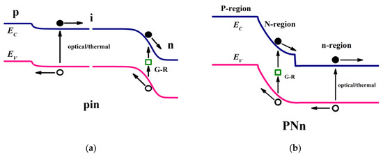
The empirical tight binding (ETB) method [20] is used to calculate the bandgap, conduction band (), and valence band () energies. The GaSb-type interfaces were used in our ETB model. The band diagrams of pin and PNn devices are shown in Figure 1. The pin device is comprised of 9 monolayer InAs/8 monolayer GaSb (9 ML/8 ML) SL designed for a cutoff wavelength of 5 (~248 meV). In the PNn structure, the P-region and N-region are comprised 6 ML/8 ML SL with a bandgap of 357 meV, while the n-region is comprised of 9 ML/8 ML SL, same as the pin device. In the PNn design, the N-region and n-region have the same GaSb sublayer thickness (8 MLs) so that there is no discontinuity in the valance band to block the photocurrent.
Figure 1.
(a) Schematic band diagram of the pin structure; (b) Schematic band diagram of the PNn structure.
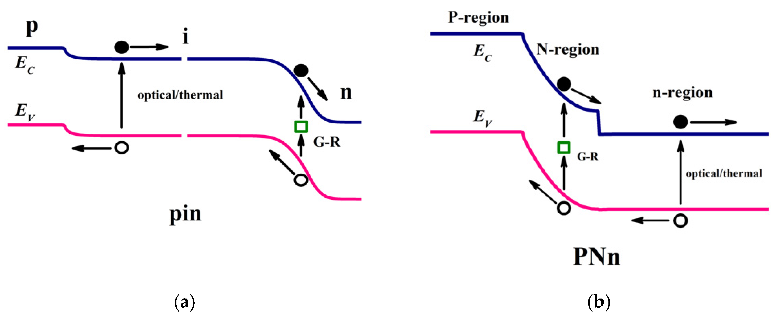
The pin and PNn devices were grown on n-type InAs substrates by MOCVD. GaAs-type interfaces were formed to compensate the compressive strain from the GaSb layers. The other growth details can be found elsewhere [21]. The epitaxial structures of both devices are shown in Figure 2. The pin structure includes a 100 nm thick n-MWSL contact layer doped to 2 1018 cm−3, a 1.7 um thick unintentionally (uid) doped MWSL absorber, a 200 nm thick p-MWSL contact layer doped to 2 1016 cm−3, a 20 nm thick p-GaSb cap doped to 2 1016 cm−3. The PNn structure consisted of a 100 nm thick n-MWSL contact layer doped to 2 1018 cm−3, a 1.7 thick n-region doped to 2 1016 cm−3, a 200 nm thick N-region doped to 4 1016 cm−3, a 250 nm thick P-region doped to 1 1018 cm−3, a 20 nm thick p-GaSb layer doped to 1 1018 cm−3. In the PNn device, the depletion region will be just within the N-region with such thickness and doping level. The undoped InAs/GaSb (9 ML/8 ML) SL absorber could be p-type in nature since undoped InAs is n-type, undoped GaSb is p-type with similar background level, and they will compensate each other, which brings uncertainty; thus, for the PNn device to work, the absorber is intentionally doped to 2 1016 cm−3. The carrier concentrations were verified by Hall measurement using lift-off test method. For material characterization and device fabrication, X-ray diffraction (XRD) was used to evaluate the structural quality of the SLs. The mesa was defined by wet chemical etching using a solution of citric acid and phosphoric acid. Sidewalls were passivated by SU-8 photoresist, and the ohmic contacts were formed by Ti/Pt/Au metal stacks. No antireflection coating was applied to the devices.
Figure 2.
Schematic structures of the PNn and pin devices.
3. Results and Discussion
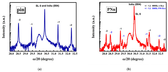
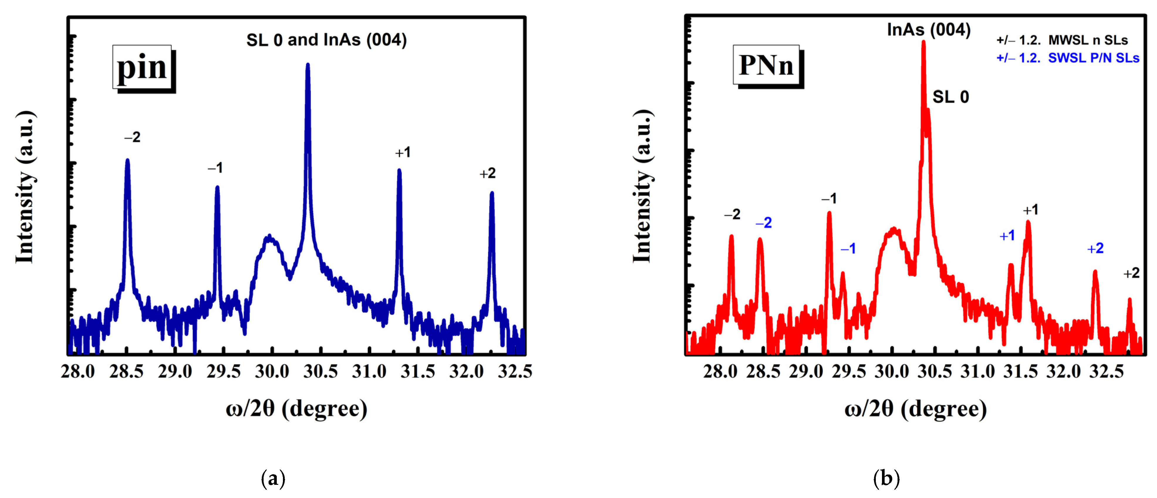
Figure 3 shows the XRD curves in -2 scan mode around InAs (004) for the pin and PNn devices. The periods for the MWSL absorbers are measured to be 5.19 nm and 5.11 nm for the pin and PNn devices, respectively, which match well with the designed thickness of 5.2 nm. Intense satellite peaks of the MWSLs were clearly observed and the full widths at half-maximum (FWHMs) of the MWSLs ± 1th order peaks were below 100 arcsec for both pin and PNn devices, suggesting a good SL structural quality.
Figure 3.
High-resolution XRD scan around InAs (004) of the pin device (a) and the PNn device (b).
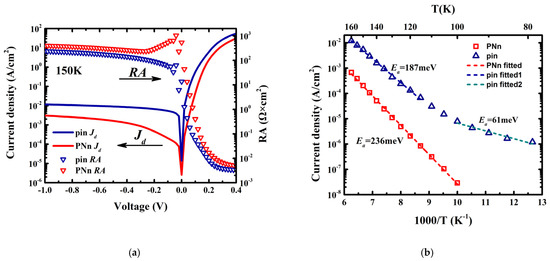
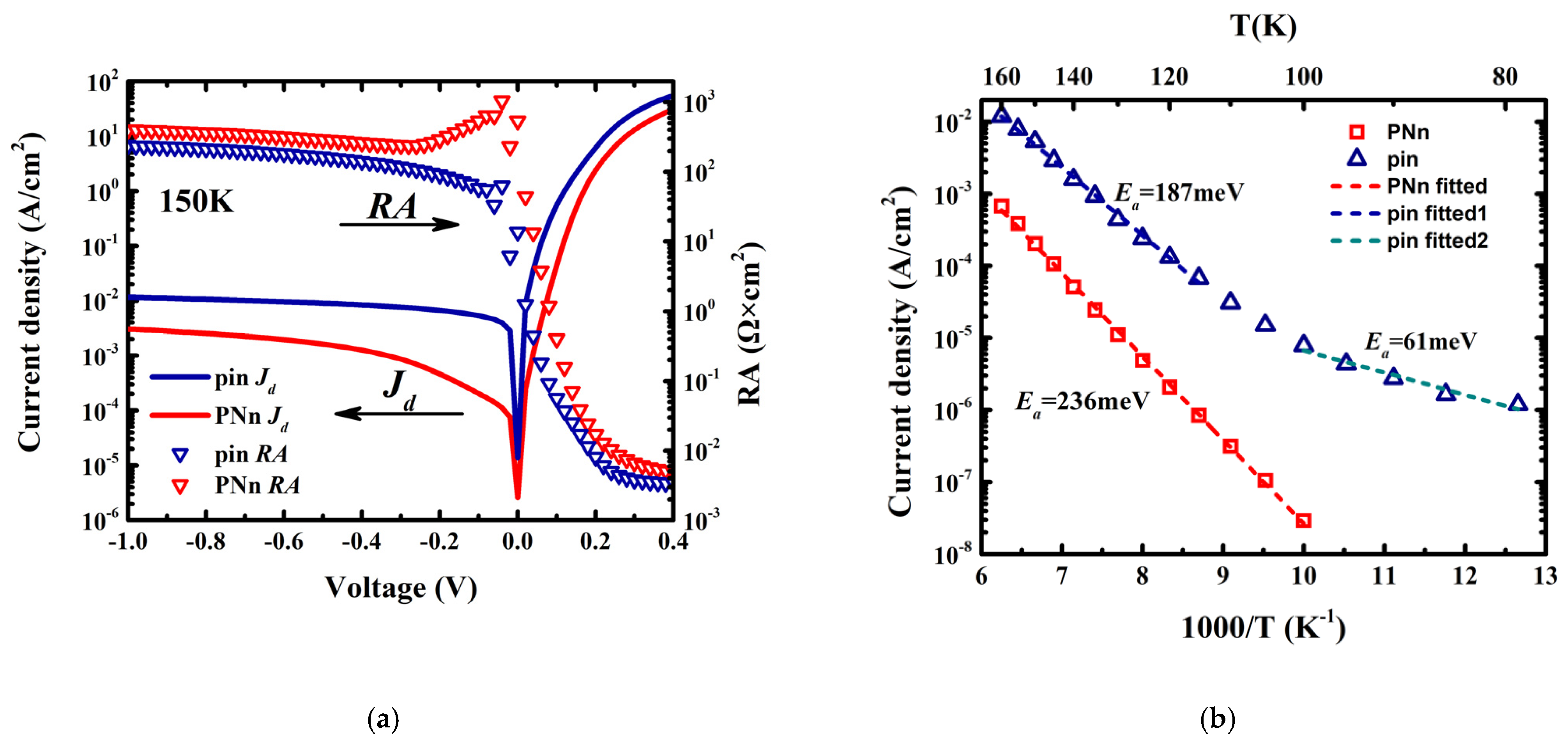
The Jd and RA as a function of the bias voltage of the two devices at 150 K are shown in Figure 4a. A dark current density of 2.05 10−4 A/cm2 and 5.35 10−3 A/cm2 was measured at −0.1 V for the PNn and the pin devices, respectively. R0A values are 150 K for the PNn and the pin devices are 540.12 and 13.74 , respectively. It can be seen that dark current is effectively suppressed in the PNn structure. The diffusion and G-R dark currents increase as the temperature rises but in different ways. The diffusion current is proportional to , whereas the G-R current is proportional to . To investigate the limiting mechanisms of the PNn and pin devices, temperature dependent current–voltage measurements were performed. Figure 4b presents the Arrhenius plot of the dark current density of the PNn and pin devices at −0.1 V applied bias. In the temperature range of 100 to 160 K, the measured dark current of the PNn device can be fitted perfectly with an activation energy of about 236 meV, which is very close to the designed n-region bandgap of 248 meV. It means that the dominant mechanism of dark current in the PNn device is the diffusion current. In comparison, the activation energy of the pin device was extracted to be 187 meV within a temperature range of 130 K to 160 K. This value is about three-fifths of the estimated bandgap energy of the 9 ML/8 ML SL, which implies the dark current mechanism involves both the diffusion and G-R currents. At 80~100 K, the dark current is only slightly sensitive to temperature and the activation energy is about 61 meV, indicating that the trap-assisted tunneling current is dominant. However, the trap-assisted tunneling current becomes insignificant and comparable to the surface contribution at small reverse bias and low temperatures; therefore, the small activation energy may also result from surface leakage.
Figure 4.
(a) The dark current density and the differential-resistance-area product as a function of applied bias measured at 150 K for both pin and PNn devices. (b) Dark current density vs. 1/T for pin and PNn device from 77 K to 160 K.
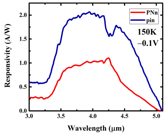
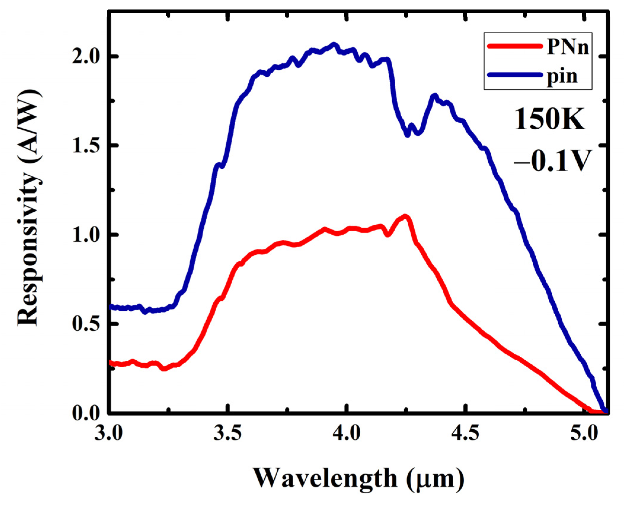
The spectral response () of the detectors was measured by the Nicolet IS50 FTIR system, calibrated by a 600 K blackbody source. The measurements were carried out under −0.1 V bias. The spectral responsivity versus wavelength at 150 K for the PNn and pin devices is shown in Figure 5. At 150 K, the PNn and pin devices exhibit a 50% cutoff wavelength of 4.5 and 4.7 , respectively. The 100% cutoff wavelength for both devices is around 5 , which is close to the design. A peak responsivity of 1.11 A/W and 2.06 A/W was achieved for the PNn and pin devices, respectively, corresponding to a quantum efficiency (QE) of 32% and 65%. The peak response of the PNn device is much lower than in the pin device, which is attributed to the higher doping level in the PNn device and thus a decreased minority diffusion length [3]. A possible potential barrier in the valence band may also account for the lower QE.
Figure 5.
Spectral responsivities of PNn and pin devices.
After the electrical and optical characterizations, the specific detectivity at −0.1 V of the PNn and pin devices was calculated using the following equation:
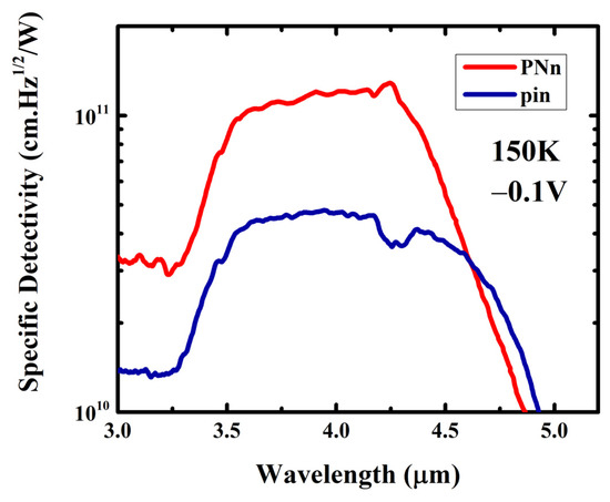
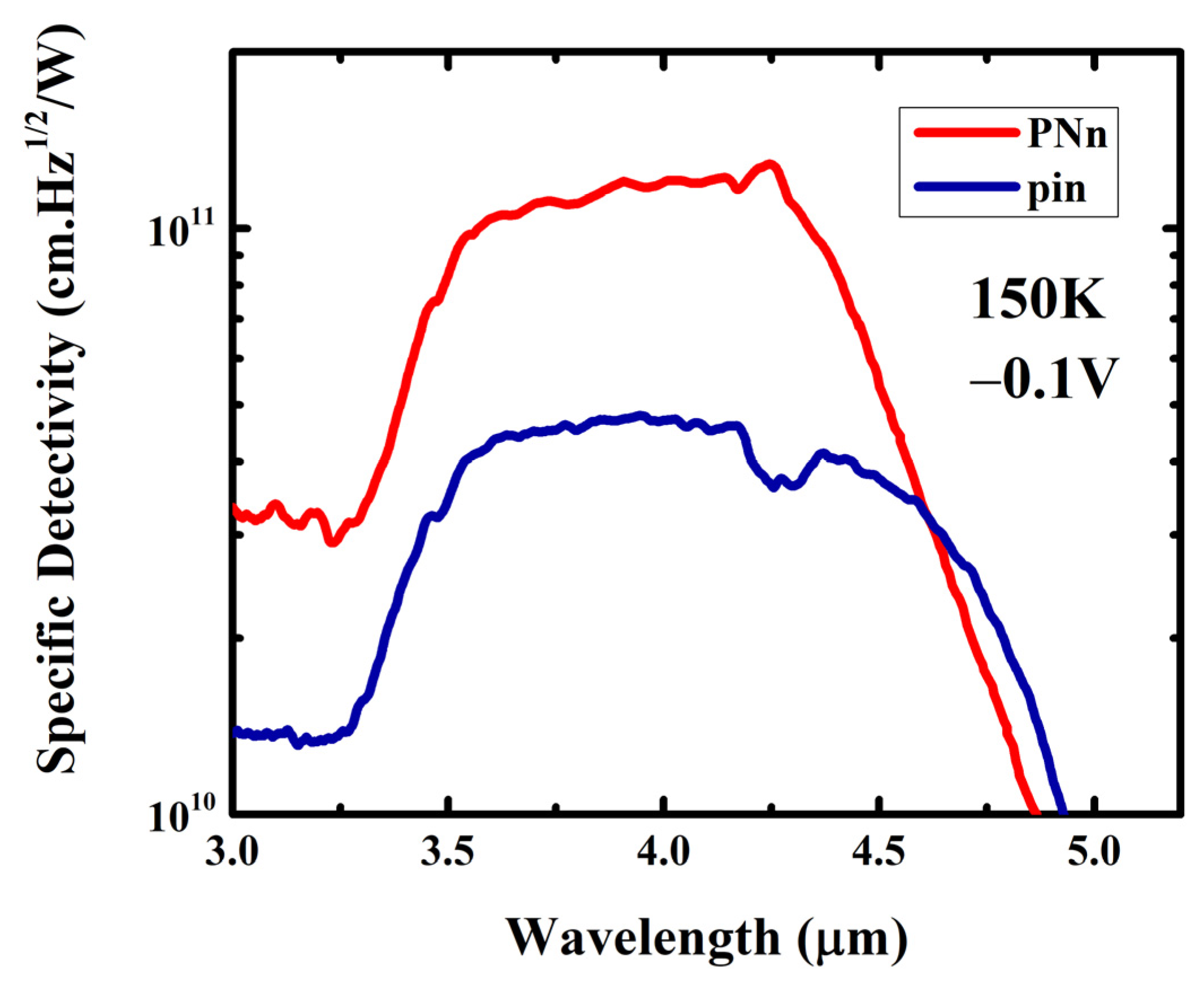
where q is the electric charge, is the dark current density, T is the temperature of the device, k is Boltzmann constant, and R and A are dynamic resistance and diode area, respectively. The calculated D* spectra for the PNn and pin devices at −0.1 V and 150 K are provided in Figure 6, and the device results are summarized in Table 1. The peak D* reaches 1.28 1011 for the PNn device, which is significantly higher than that of the pin device and comparable with those reported for MBE-grown devices with advanced design at similar cutoff wavelengths, with D* ranging from 3.4 1010 to 7.1 1011 [7,8,9,10,12,22,23]. The results of Refs. [10,15] are also shown in the Table 1. It can be seen that there is still substantial room for improvement in both optical and electrical performance of the PNn device. The relatively low QE of the PNn device can be improved by lowering the doping level [24]. A further improvement of the device performance can be expected if a p-type absorber and corresponding double heterostructure structure can be used. By using the p-type absorber, the minority carriers are electrons, which have a higher carrier lifetime leading to an improved QE and reduced diffusion current. Moreover, eliminating potential barriers by optimizing the device structure and doping concentration is also a feasible direction to improve the QE of the device.
Figure 6.
Specific detectivity spectra of the PNn and pin devices.
Table 1.
Summary of the device results at 150 K.
4. Conclusions
In summary, we have investigated mid-wavelength InAs/GaSb SL infrared photodetectors with an Al-free single heterojunction design and a pin homojunction design grown by MOCVD. Their performances have been compared by electrical and optical characterizations. In the PNn heterojunction, a wider-gap barrier layer was inserted between the absorber and the p-contact. XRD scan shows reasonably good structural quality for both devices. Arrhenius plots of the dark current of the PNn device were compared with the pin device. In the temperature range of 100 K to 160 K, the PNn and the pin devices demonstrated an activation energy of 230 meV and 187 meV, respectively, indicating that the PNn structure has successfully suppressed the G-R current and achieved a diffusion-limited behavior, while the pin device is dominated by both the G-R current and diffusion current. At 150 K, the pin device shows a peak QE of 65% and the PNn device shows a peak QE of 32% due to the intentionally-doped n-type absorber. At 150 K and a bias voltage of −0.1 V, the PNn device with a 50% cutoff of 4.5 shows a dark current density of 2.05 10−4 A/cm2 and a peak D* of 1.28 1011 .
Author Contributions
Software, M.L.; investigation, H.Z. (He Zhu), J.L., H.Z. (Hong Zhu) and Y.H. (Yong Huang); data curation, Y.H. (Yunlong Huai) and Z.L.; writing—original draft preparation, H.Z. (He Zhu); writing—review and editing, Y.H. (Yong Huang) and H.Z. (He Zhu). All authors have read and agreed to the published version of the manuscript.
Funding
This research was funded by the National Natural Science Foundation of China, grant number 61874179, 61804161, 62074156, 11874390.
Institutional Review Board Statement
Not applicable.
Informed Consent Statement
Not applicable.
Data Availability Statement
The data that support the findings of this study are available from the corresponding author upon reasonable request.
Acknowledgments
The authors are grateful for the technical support from the School of Physical Science and Technology, ShanghaiTech University.
Conflicts of Interest
The authors declare no conflict of interest.
References
- Martyniuk, P.; Rogalski, A. HOT Infrared Photodetectors. Opto-Electron. Rev. 2013, 21, 239–257. [Google Scholar] [CrossRef] [Scilit]
- Manissadjian, A.; Rubaldo, L.; Rebeil, Y.; Kerlain, A.; Brellier, D.; Mollard, L. Improved IR Detectors to Swap Heavy Systems for SWaP. In Proceedings of the SPIE Defense, Security, and Sensing, Baltimore, MD, USA, 1 May 2012; Andresen, B.F., Fulop, G.F., Norton, P.R., Eds.; pp. 835334–835339. [Google Scholar]
- Kinch, M.A. State-of-the-Art Infrared Detector Technology; SPIE Press: Bellingham, WA, USA, 2014; ISBN 978-1-62841-289-5. [Google Scholar]
- Rogalski, A.; Martyniuk, P.; Kopytko, M. Type-II Superlattice Photodetectors versus HgCdTe Photodiodes. Prog. Quantum Electron. 2019, 68, 100228. [Google Scholar] [CrossRef] [Scilit]
- Haugan, H.J.; Olson, B.V.; Brown, G.J.; Kadlec, E.A.; Kim, J.K.; Shaner, E.A. Significantly Enhanced Carrier Lifetimes of Very Long-Wave Infrared Absorbers Based on Strained-Layer InAs/GaInSb Superlattices. Opt. Eng. 2017, 56, 091604. [Google Scholar] [CrossRef] [Scilit]
- Maimon, S.; Wicks, G.W. NBn Detector, an Infrared Detector with Reduced Dark Current and Higher Operating Temperature. Appl. Phys. Lett. 2006, 89, 151109. [Google Scholar] [CrossRef] [Scilit]
- Razeghi, M.; Abdollahi Pour, S.; Huang, E.; Chen, G.; Haddadi, A.; Nguyen, B. Type-II InAs/GaSb Photodiodes and Focal Plane Arrays Aimed at High Operating Temperatures. Opto-Electron. Rev. 2011, 19, 261–269. [Google Scholar] [CrossRef] [Scilit]
- Sun, Y.; Wang, G.; Han, X.; Xiang, W.; Jiang, D.; Jiang, Z.; Hao, H.; Lv, Y.; Guo, C.; Xu, Y.; et al. 320 × 256 High Operating Temperature Mid-Infrared Focal Plane Arrays Based on Type-II InAs/GaSb Superlattice. Superlattices Microstruct. 2017, 111, 783–788. [Google Scholar] [CrossRef] [Scilit]
- Chen, G.; Haddadi, A.; Hoang, A.-M.; Chevallier, R.; Razeghi, M. Demonstration of Type-II Superlattice MWIR Minority Carrier Unipolar Imager for High Operation Temperature Application. Opt. Lett. 2015, 40, 45. [Google Scholar] [CrossRef] [Scilit]
- Ting, D.Z.; Soibel, A.; Khoshakhlagh, A.; Rafol, S.B.; Keo, S.A.; Höglund, L.; Fisher, A.M.; Luong, E.M.; Gunapala, S.D. Mid-Wavelength High Operating Temperature Barrier Infrared Detector and Focal Plane Array. Appl. Phys. Lett. 2018, 113, 021101. [Google Scholar] [CrossRef] [Scilit]
- Soibel, A.; Ting, D.Z.; Rafol, S.B.; Fisher, A.M.; Keo, S.A.; Khoshakhlagh, A.; Gunapala, S.D. Mid-Wavelength Infrared InAsSb/InAs NBn Detectors and FPAs with Very Low Dark Current Density. Appl. Phys. Lett. 2019, 114, 161103. [Google Scholar] [CrossRef] [Scilit]
- Wu, D.; Li, J.; Dehzangi, A.; Razeghi, M. Mid-Wavelength Infrared High Operating Temperature PBn Photodetectors Based on Type-II InAs/InAsSb Superlattice. AIP Adv. 2020, 10, 025018. [Google Scholar] [CrossRef] [Scilit]
- Juergensen, H. MOCVD Technology in Research, Development and Mass Production. Mater. Sci. Semicond. Process. 2001, 4, 467–474. [Google Scholar] [CrossRef] [Scilit]
- Huang, Y.; Ryou, J.-H.; Dupuis, R.D.; Zuo, D.; Kesler, B.; Chuang, S.-L.; Hu, H.; Kim, K.-H.; Ting Lu, Y.; Hsieh, K.C.; et al. Strain-Balanced InAs/GaSb Type-II Superlattice Structures and Photodiodes Grown on InAs Substrates by Metalorganic Chemical Vapor Deposition. Appl. Phys. Lett. 2011, 99, 011109. [Google Scholar] [CrossRef] [Scilit]
- Wu, D.; Dehzangi, A.; Razeghi, M. Demonstration of Mid-Wavelength Infrared NBn Photodetectors Based on Type-II InAs/InAs1-xSbx Superlattice Grown by Metal-Organic Chemical Vapor Deposition. Appl. Phys. Lett. 2019, 115, 061102. [Google Scholar] [CrossRef] [Scilit]
- Teng, Y.; Zhao, Y.; Wu, Q.; Li, X.; Hao, X.; Xiong, M.; Huang, Y. High-Performance Long-Wavelength InAs/GaSb Superlattice Detectors Grown by MOCVD. IEEE Photon. Technol. Lett. 2019, 31, 185–188. [Google Scholar] [CrossRef] [Scilit]
- Zhao, Y.; Teng, Y.; Hao, X.; Wu, Q.; Miao, J.; Li, X.; Xiong, M.; Huang, Y. Optimization of Long-Wavelength InAs/GaSb Superlattice Photodiodes With Al-Free Barriers. IEEE Photon. Technol. Lett. 2020, 32, 19–22. [Google Scholar] [CrossRef] [Scilit]
- Zhu, H.; Hao, X.; Teng, Y.; Liu, J.; Zhu, H.; Li, M.; Huai, Y.; Huang, Y. Long-Wavelength InAs/GaSb Superlattice Detectors With Low Dark Current Density Grown by MOCVD. IEEE Photon. Technol. Lett. 2021, 33, 429–432. [Google Scholar] [CrossRef] [Scilit]
- Yang, Q.K.; Fuchs, F.; Schmitz, J.; Pletschen, W. Investigation of Trap-Assisted Tunneling Current in InAs/(GaIn)Sb Superlattice Long-Wavelength Photodiodes. Appl. Phys. Lett. 2002, 81, 4757–4759. [Google Scholar] [CrossRef] [Scilit]
- Wei, Y.; Razeghi, M. Modeling of Type-II InAs/GaSb Superlattices Using an Empirical Tight-Binding Method and Interface Engineering. Phys. Rev. B 2004, 69, 085316. [Google Scholar] [CrossRef] [Scilit]
- Li, X.; Zhao, Y.; Wu, Q.; Teng, Y.; Hao, X.; Huang, Y. Exploring the Optimum Growth Conditions for InAs/GaSb and GaAs/GaSb Superlattices on InAs Substrates by Metalorganic Chemical Vapor Deposition. J. Cryst. Growth 2018, 502, 71–75. [Google Scholar] [CrossRef] [Scilit]
- Plis, E.; Klein, B.; Myers, S.; Gautam, N.; Smith, E.P.; Krishna, S. High Operating Temperature Midwave Infrared InAs/GaSb Superlattice Photodetectors on (111) GaSb Substrates. IEEE Electron. Device Lett. 2013, 34, 426–428. [Google Scholar] [CrossRef] [Scilit]
- Ramirez, D.A.; Plis, E.A.; Myers, S.A.; Morath, C.P.; Cowan, V.M.; Krishna, S. High-Operating Temperature MWIR Unipolar Barrier Photodetectors Based on Strained Layer Superlattices. In Proceedings of the Infrared Technology and Applications XLI, Baltimore, MD, USA, 4 June 2015; Andresen, B.F., Fulop, G.F., Hanson, C.M., Norton, P.R., Eds.; p. 945113. [Google Scholar]
- Nguyen, B.-M.; Hoffman, D.; Wei, Y.; Delaunay, P.-Y.; Hood, A.; Razeghi, M. Very High Quantum Efficiency in Type-II InAs/GaSb Superlattice Photodiode with Cutoff of 12 μm. Appl. Phys. Lett. 2007, 90, 231108. [Google Scholar] [CrossRef] [Scilit]

Publisher’s Note: MDPI stays neutral with regard to jurisdictional claims in published maps and institutional affiliations. |
© 2021 by the authors. Licensee MDPI, Basel, Switzerland. This article is an open access article distributed under the terms and conditions of the Creative Commons Attribution (CC BY) license (https://creativecommons.org/licenses/by/4.0/).