


Abstract
RF photonics has emerged as a key technology for the generation and processing of high-frequency RF signals required in 6G wireless communications, photonic radar, and high-resolution sensing systems. In particular, optical heterodyning-based RF signal generation offers the advantage of controlling the RF frequency through optical wavelength tuning. In this study, a dual-wavelength external cavity laser based on a fluorinated polyimide photonic integrated circuit is designed and fabricated. The photonic integrated circuit incorporates waveguide Bragg gratings, thermo-optic phase modulators, and a 2 × 2 multimode interference coupler to realize two external cavity lasers and combine their outputs on a single chip. The high thermo-optic efficiency of the polymer waveguides enables wide and continuous laser wavelength tuning. Based on this tuning capability, optical heterodyne RF signal generation is experimentally demonstrated using the dual-wavelength external cavity laser. The measured RF frequencies closely match the calculated values obtained from the optical wavelength differences. Continuous RF frequency tuning through Bragg wavelength and cavity mode tuning was experimentally demonstrated up to the measurement-limited frequency of 40 GHz, confirming the feasibility of polymer photonic integrated circuits for compact and widely tunable RF photonic sources.
1. Introduction
The generation and processing of high-frequency RF signals are essential for a wide range of applications, including radar, wireless communications, and sensing systems. In particular, high-frequency RF signals enable wide transmission bandwidths and high-resolution measurements and play a crucial role in next-generation communication and precision sensing systems [1,2]. However, as the RF frequency increases, conventional electronic approaches for RF signal generation and processing face fundamental challenges, including bandwidth limitations imposed by the finite response speed of charge carriers, increased transmission losses, electromagnetic interference (EMI), and circuit complexity [3,4,5].
To overcome these limitations, RF photonics has emerged as an alternative approach, as signals can be generated and processed in the optical frequency domain, thereby overcoming the high-frequency limitations of conventional electronic approaches [6]. In particular, optical heterodyning-based RF sources offer wide frequency tunability and stable high-frequency signal generation, making them attractive for various RF photonic applications [7]. Extensive research has been conducted on their applications in millimeter-wave (mmWave) photonic radar, 6G wireless communications, high-resolution imaging, and sensing systems [8,9,10].
The implementation of RF photonic signal generation on a photonic integrated circuit (PIC) enables mass production while improving operational stability through on-chip optical signal generation and processing. In addition, the integration of optical sources, modulators, and photonic components reduces the system footprint, while wafer-scale fabrication enables high reproducibility of device characteristics. With these advantages, extensive research has been conducted on PIC-based RF photonic devices [11,12,13,14,15]. In particular, THz-band signals were generated through optical heterodyning using a PIC-based tunable laser, and wireless data transmission using the THz signals was demonstrated [14]. Furthermore, a transceiver architecture incorporating lasers and an optical frequency comb generator was proposed on a PIC for THz wireless communication [15].
Since the generated RF frequency is determined by the wavelength difference between two optical sources, tunable lasers with wide wavelength tunability play an important role in optical-heterodyning-based RF photonics systems. External cavity lasers (ECLs) have been widely used as tunable laser sources because they provide a wide tuning range and excellent wavelength selectivity. In waveguide-based ECLs, the materials used for the external cavity significantly affect the wavelength tuning characteristics. Si- and Si3N4-based PICs can achieve a wide tuning range using Vernier structures, whereas continuous wavelength tuning is limited by their structural characteristics [16,17,18,19,20]. In contrast, polymer-based PICs can effectively tune the Bragg wavelengths and cavity modes with their high thermo-optic (TO) coefficient and low thermal conductivity. These characteristics enable both a wide RF tuning range and continuous tuning in optical-heterodyning-based RF signal generation [21,22,23,24,25,26]. Based on these advantages, a polymer-PIC-based dual-wavelength ECL (2-λ ECL) was designed and fabricated in this study.
Fluorinated polyimide has high thermal stability, enabling the maintenance of stable characteristics under temperature variations. Moreover, the environmental reliability of polymer thermo-optic devices has been demonstrated in commercial variable optical attenuators (VOAs) [27]. These properties contribute to the environmental stability of the TO tuning elements in the proposed 2-λ ECL. In addition, the substitution of C–H bonds with C–F bonds shifts the absorption bands to longer wavelengths, resulting in low optical absorption in the 1550 nm wavelength band [28,29,30]. Among fluorinated polymer materials, fluorinated polyimide exhibits a high refractive index, enabling the design of high-index-contrast single-mode waveguides and making it suitable for photonic circuit implementation for hybrid integration with InP SLD gain chips [31,32,33]. The proposed PIC is based on a single-mode waveguide with a fluorinated polyimide core. Based on this waveguide, Bragg gratings, TO phase modulators, and a 2 × 2 MMI coupler were designed and fabricated. By integrating these components into a single chip, a 2-λ ECL was implemented, and RF signal generation through optical heterodyning was experimentally demonstrated.
2. Design of Polymer Waveguide Device for 2-λ ECL
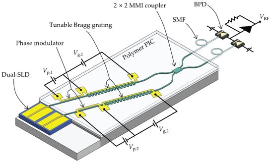
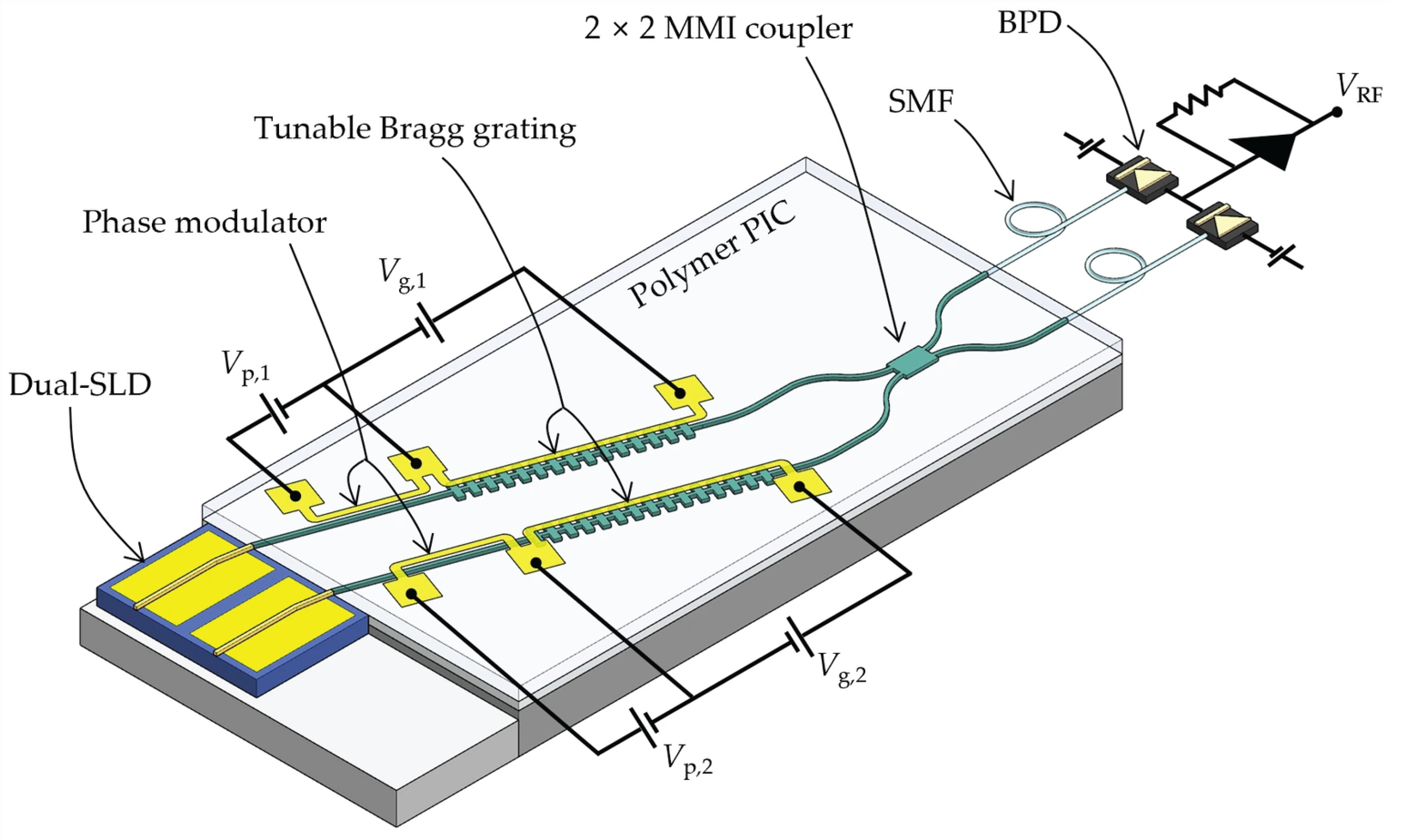
The proposed 2-λ ECL was designed based on PIC technology to integrate two tunable lasers and combine their outputs. The schematic diagram of the polymer PIC-based 2-λ ECL is shown in Figure 1. The device incorporates two ECLs on a single PIC, and the two optical signals are combined using a 2 × 2 MMI coupler. The combined optical signals generate an RF beating signal through optical heterodyning corresponding to the difference between the two optical frequencies.
Figure 1.
Schematicof the 2-λ ECL consisting of a polymer PIC butt-coupled to a dual-SLD gain chip. The polymer PIC integrates tunable Bragg gratings, TO phase modulators, and a 2 × 2 MMI coupler where each Bragg grating and the corresponding SLD form an ECL. The Bragg reflection wavelengths and cavity modes are independently tuned by the grating heaters and TO phase modulators using the control voltages Vg and Vp, respectively. The optical outputs from the two ECLs are combined by the 2 × 2 MMI coupler and guided to a balanced photodetector (BPD) through single-mode fibers (SMFs). The photomixed RF signal is extracted from the BPD as the RF output signal VRF.
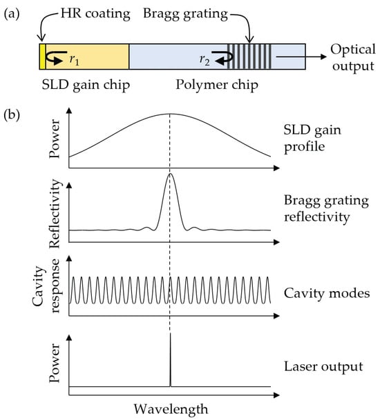
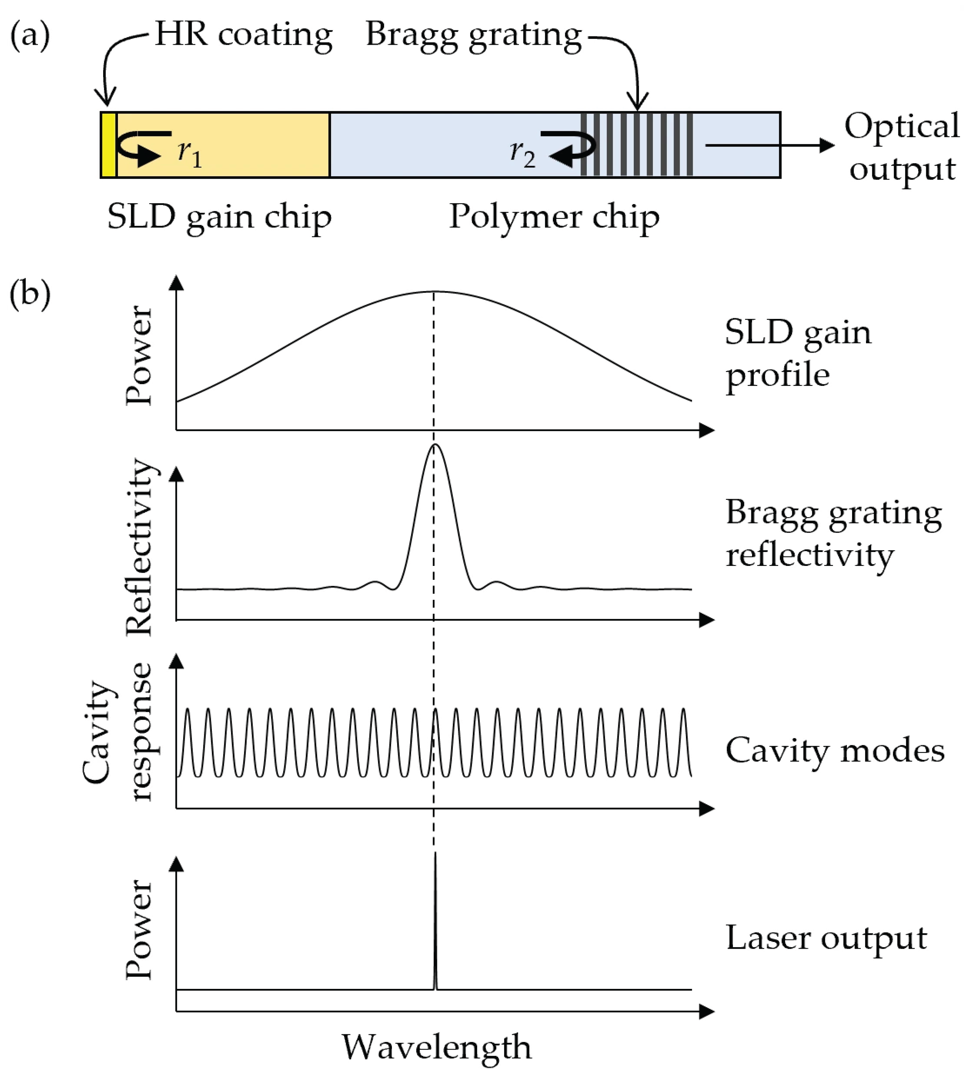
The ECLs are fabricated by butt-coupling an SLD gain chip to a polymer PIC, as shown in Figure 2a, and laser cavities are formed between the HR-coated SLD and the Bragg grating on the PIC. In this structure, the lasing wavelength is selected by the mode with the highest net gain resulting from the overlap of the SLD gain profile, Bragg grating reflectivity, and cavity modes, as shown in Figure 2b.
Figure 2.
(a) Schematic of the ECL composed of an SLD gain chip and a polymer chip with a waveguide Bragg grating. (b) Illustration of the ECL operation showing the SLD gain spectrum, Bragg grating reflectivity, cavity modes, and the resulting laser output determined by the maximum net gain.
A polymer PIC was designed to implement the 2-λ ECL. A Si wafer with a 3-μm-thick thermally oxidized SiO2 layer was used as the substrate, where the SiO2 layer served as the lower cladding. Fluorinated polyimide was used for the core, and ZPU13-430 was used for the upper cladding. The refractive indices of the polyimide core, ZPU13-430 upper cladding, and SiO2 lower cladding at 1550 nm for TE polarization were 1.5613, 1.430, and 1.4458, respectively. A single-mode waveguide with dimensions of 2 × 1.5 μm2 was designed using the effective index method.
To maximize the coupling efficiency between the SLD gain chip and the polymer PIC, the input waveguide tilt angle was determined by considering the tilted output waveguide of the SLD gain chip. Since the output waveguide of the SLD gain chip was tilted by 9° to suppress end-facet reflections, the input waveguide of the polymer PIC was tilted by 20° based on the calculated effective index and Snell’s law.
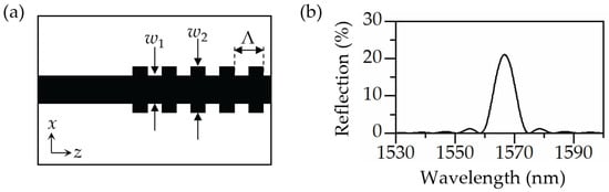
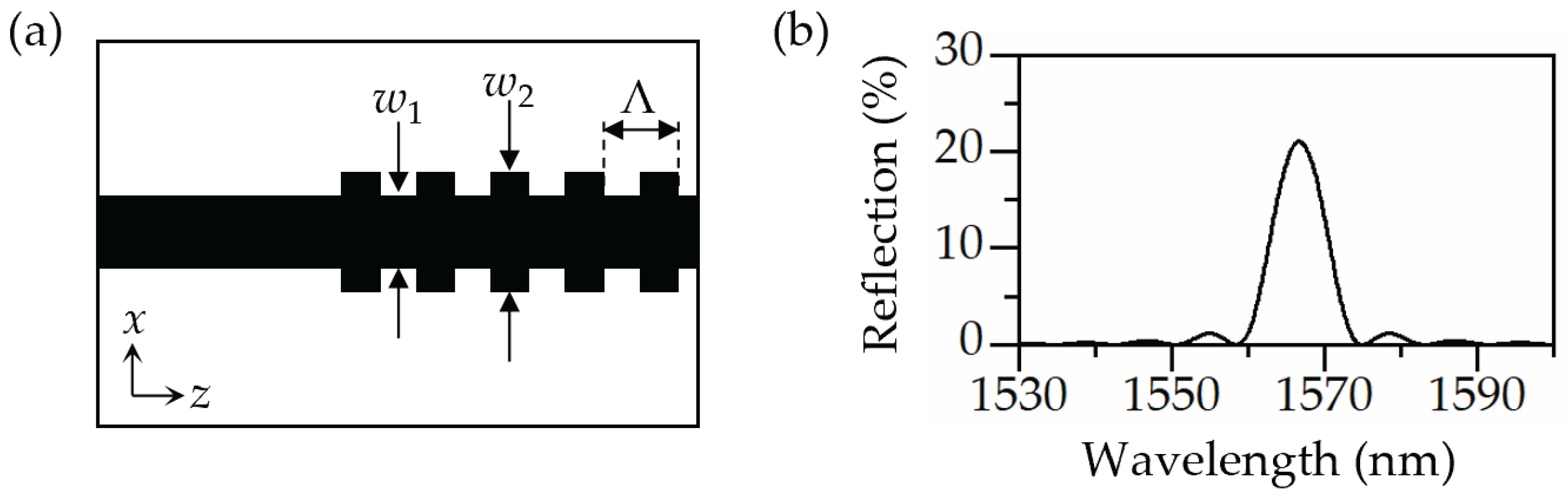
The Bragg grating was designed to have a reflection peak near 1550 nm. As shown in Figure 3a, a sidewall-corrugated waveguide Bragg grating structure was employed. To maintain single-mode operation while ensuring sufficient refractive index modulation, the Bragg grating widths w1 and w2 were set to 2 μm and 3 μm, respectively. Considering the resolution limitation of the contact lithography process, the third-order Bragg condition, which requires a grating period Λ three times longer than that of a first-order Bragg grating at the same Bragg wavelength λB, was adopted, and Λ was set to 1.56 μm. The calculated reflection spectrum of the Bragg grating with an ideal rectangular profile, obtained using the transfer matrix method (TMM), is shown in Figure 3b, confirming that a peak reflectivity of 21% can be achieved at a grating length of lg = 100 μm [34].
Figure 3.
(a) Schematic of the waveguide Bragg grating with w1 = 2 μm, w2 = 3 μm, and a third-order grating period Λ = 1.56 μm. (b) Calculated reflection spectrum of the Bragg grating obtained using the transfer matrix method.
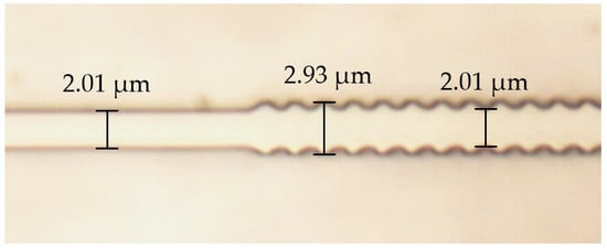
Meanwhile, sidewall rounding may occur due to the characteristics of the contact lithography process, making it difficult to define the designed rectangular grating profile. To confirm this, a test device was fabricated, and the results of the optical microscope image analysis are shown in Figure 4, confirming that a sinusoidal-like sidewall profile resulted from fabrication-induced sidewall rounding.
Figure 4.
Microscope image of the fabricated polymer Bragg grating test structure showing a sinusoidal-like sidewall profile caused by fabrication-induced sidewall rounding.
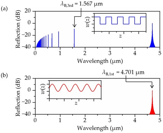
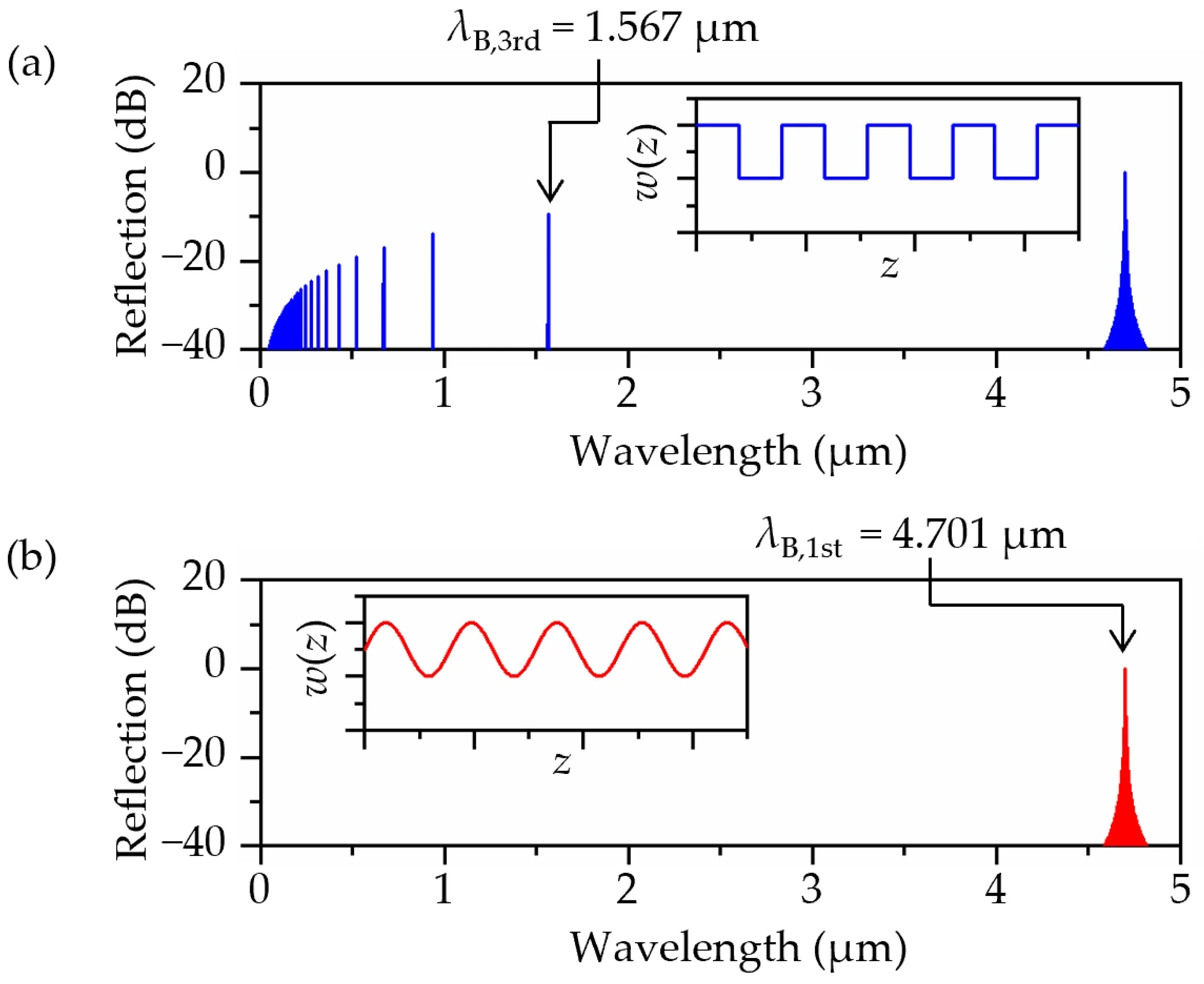
To analyze the effect of the sidewall profile on Bragg reflection, Fourier analysis was performed, and the detailed theoretical derivation is provided in Appendix A. For the rectangular sidewall profile shown in Figure 5a, higher-order Fourier components produce multiple Bragg reflection peaks. The mth-order Bragg condition is given by λB,m = 2ΛNeff/m, where Λ is the grating period, Neff is the effective refractive index, and m is the Bragg order. Accordingly, the first- and third-order Bragg wavelengths were calculated to be 4.701 μm and 1.567 μm, respectively. In contrast, for a perfectly sinusoidal sidewall profile, no Fourier component corresponding to the third-order Bragg condition exists, resulting in the absence of third-order Bragg reflection, as shown in Figure 5b. Therefore, the reduction in reflectivity caused by sidewall rounding should be considered in the design of third- or higher-order Bragg gratings, and lg should be increased to compensate for this effect. Based on this analysis, lg was designed to satisfy the target reflectivity, and it was found that a length of approximately 921 μm was required to achieve a reflectivity of 20%. The detailed design procedure is provided in Appendix A.
Figure 5.
Fourieranalysis of waveguide Bragg gratings with different width profiles, showing the corresponding grating profiles in the insets. (a) Reflection spectrum of the rectangular profile, exhibiting multiple higher-order reflection components where the third-order Bragg wavelength λB,3rd is 1.567 μm. (b) Reflection spectrum of the sinusoidal profile, where higher-order reflection components are suppressed, leaving only the first-order Bragg reflection, with first-order Bragg wavelength λB,1st indicated at 4.701 μm.
A TO phase modulator employing a Cr–Au thin film was designed for Bragg wavelength tuning and cavity mode tuning of the ECL. The design was based on the method reported in [30], and its TO characteristics were analyzed using Lumerical simulations. The effective TO coefficient with respect to the heater temperature was calculated to be −2.31 × 10⁻⁵ K−1, and the power required for a π phase shift, Pπ, was found to be 22.8 mW.
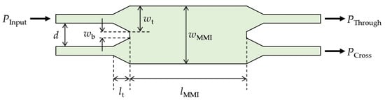
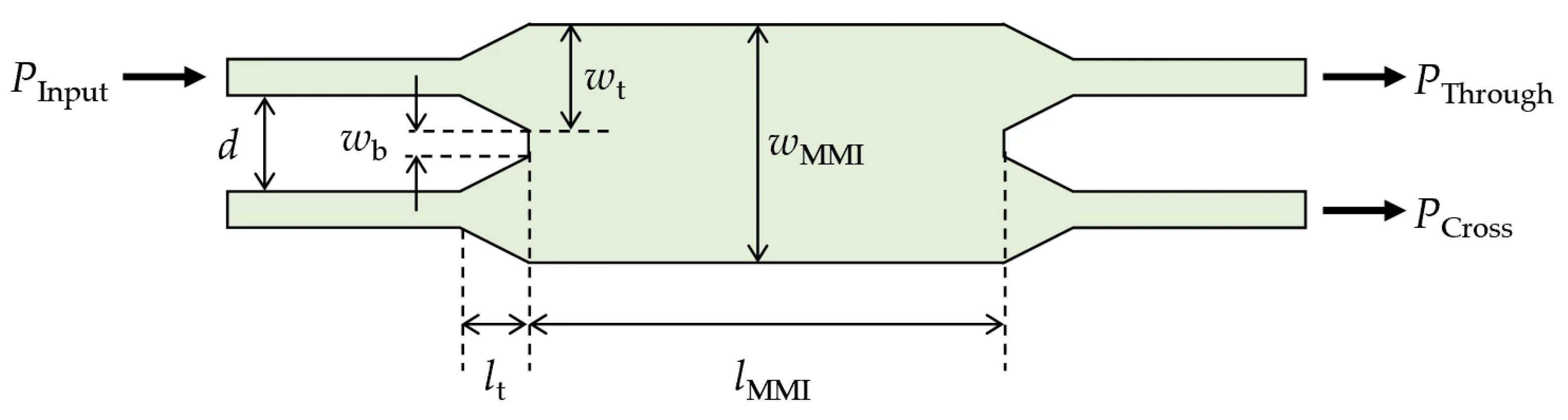
A 2 × 2 MMI coupler was designed to combine two optical signals of different wavelengths, and its schematic diagram is shown in Figure 6. Considering the minimum spacing required to prevent coupling between adjacent waveguides, the separation distance d of 5 μm was used for both the input and output waveguides. In addition, taper structures were employed at the ports to minimize optical loss. The taper width wt and taper length lt were designed to be 4 μm and 10 μm, respectively, resulting in a blunt width wb of 1 μm. The MMI width wMMI was designed to be 9 μm to enable efficient coupling to the symmetric modal field while providing ideal self-imaging characteristics and low loss. A three-dimensional beam propagation method (3D BPM) simulation was performed to optimize the MMI length lMMI. The splitting ratio and excess loss were evaluated as functions of lMMI, and the optimum length was determined to achieve a 50% splitting ratio with minimum excess loss. The optimum condition was obtained at lMMI = 179 μm.
Figure 6.
Schematic of the 2 × 2 MMI coupler illustrating the design parameters, with the distance between adjacent waveguides d, blunt width wb, taper width wt, taper length lt, MMI width wMMI, and MMI length lMMI.
To generate RF signals based on optical heterodyning, a structure that combines the outputs of two ECLs was designed. The optical signals from the two lasers were combined through a coupler, and a beating signal corresponding to the frequency difference between the two lasers was generated and detected by a photodetector (PD). Due to the low-pass filtering effect resulting from the finite response bandwidth of the PD, the optical frequency components are suppressed, and only the RF beating signal is detected.
Two ECLs were designed to initially operate at the same wavelength using identical Bragg grating structures. The Bragg wavelengths were then tuned using grating heaters to introduce a lasing wavelength difference between the two lasers, thereby generating RF signals through optical heterodyning. In addition, the optical path lengths of the cavities were controlled using the cavity phase modulators, enabling continuous and fine tuning of the output wavelengths and RF frequencies without mode hopping.
3. Fabrication of the 2-λ ECL Device
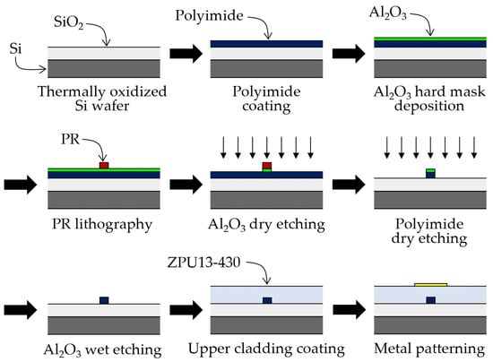
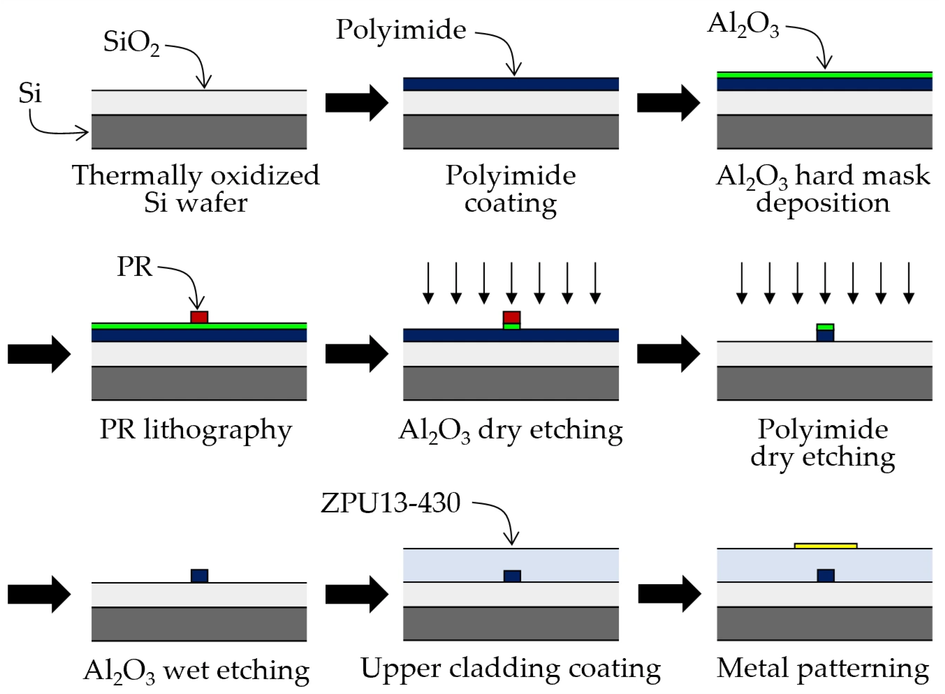
The polymer PIC integrating the designed optical components was fabricated using a wafer-level process, and the fabrication procedure is shown in Figure 7. A thermally oxidized Si wafer was used as the substrate, on which a 1.5-μm-thick polyimide core layer was formed by spin coating. To define the waveguide patterns, a 20-nm-thick Al2O3 layer was deposited by atomic layer deposition (ALD) and used as a hard mask. After photolithography using AZ MiR 701 photoresist (Merck), the Al2O3 hard mask patterns were defined by BCl3 plasma etching, followed by O2 plasma etching of the polyimide core to form the waveguide structures. The residual Al2O3 hard mask was removed by wet etching, and ZPU13-430 polymer was spin-coated to form the upper cladding. Finally, Cr and Au thin films with thicknesses of 10 nm and 100 nm, respectively, were deposited, and the TO phase modulator patterns were defined by photolithography using AZ 5214E photoresist (Merck), followed by metal wet-etching.
Figure 7.
Fabricationprocess of the polymer PIC. A thermally oxidized Si substrate is used as the lower cladding, followed by polyimide coating. An Al2O3 hard mask is deposited by ALD and patterned by photolithography and dry etching. The polyimide core waveguides are then defined by dry etching using the Al2O3 hard mask, and the remaining Al2O3 is subsequently removed by wet etching. Finally, the upper cladding is formed using ZPU13-430 polymer (ChemOptics Inc.), and metal patterns for the TO phase modulators are defined.
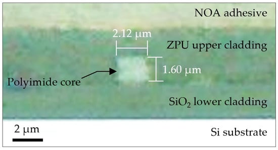
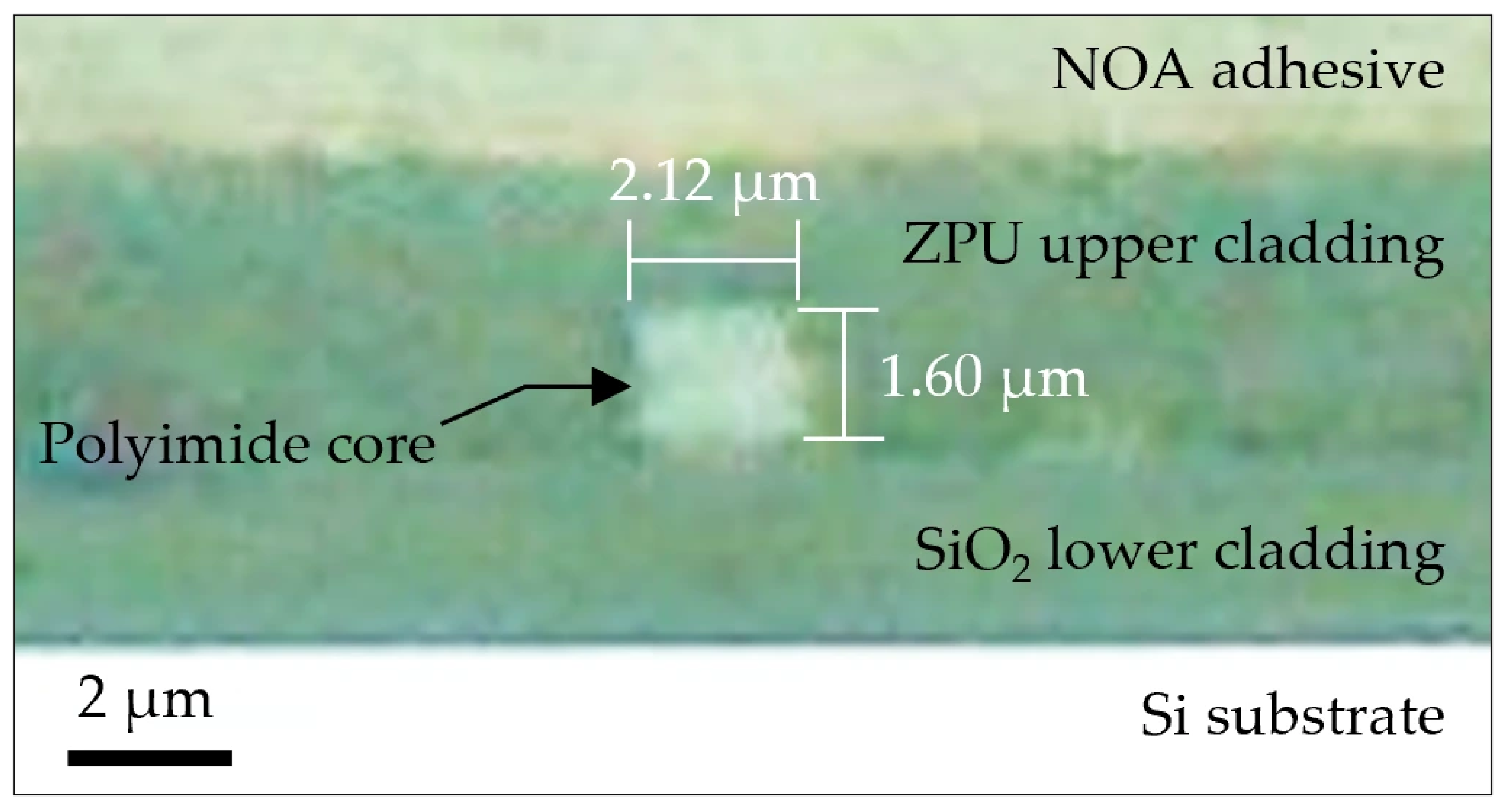
Dicing and polishing were performed for coupling to SMFs and the SLD gain chip, and microscope images of the polished facet are shown in Figure 8. From the cross-sectional image, the structure consisting of a Si substrate, SiO2 lower cladding, a polyimide core, and ZPU upper cladding can be identified.
Figure 8.
Microscope image of the polished end facet. The layered structure consists of Si substrate, SiO2 lower cladding, polyimide core, ZPU13-430 upper cladding, and NOA adhesive layer used for glass lid attachment.
The characteristics of the designed optical components were measured to confirm the optical properties of the polymer PIC. The insertion loss of a straight waveguide with a length of 1 cm was measured to be 3.44 dB using UHNA4 single-mode fibers, and the propagation loss and coupling loss were calculated from the cut-back method to be 1.47 dB/cm and 1.07 dB/facet, respectively.
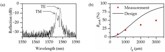
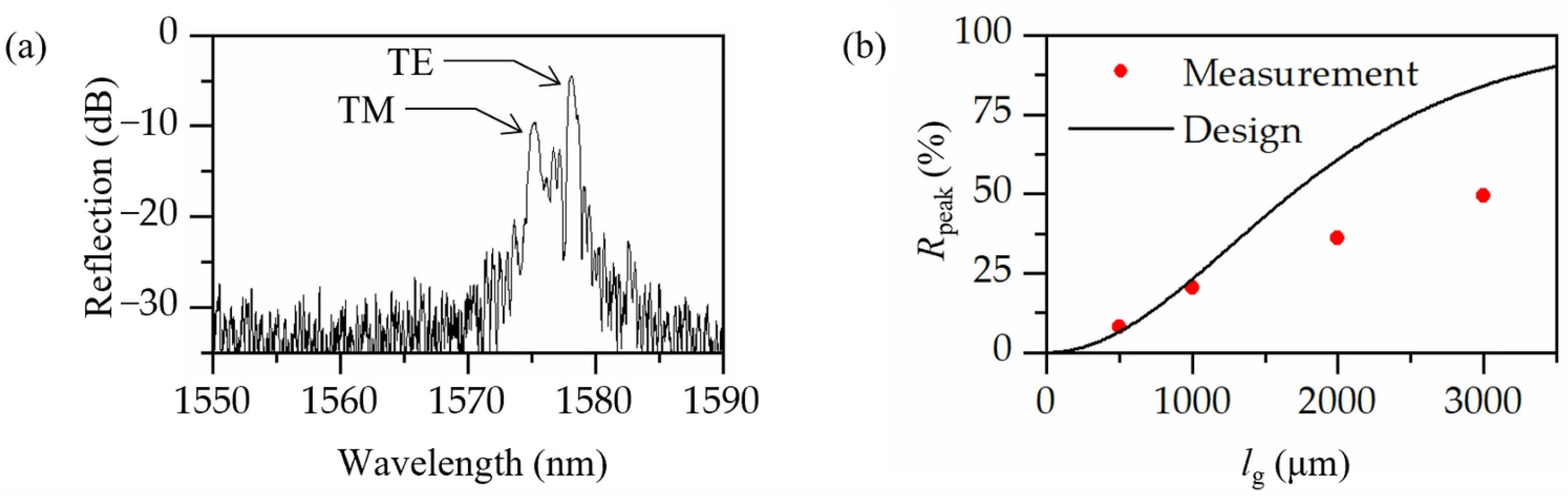
The measured reflection spectrum of the Bragg grating device is shown in Figure 9a. The spectrum was obtained for lg = 2 mm, which was selected to achieve a reflectivity of over 30% and used in the 2-λ ECL device. The reflection spectrum was measured using an SLD source with a polarization controller. Although the polarization controller can optimize the polarization state at a specific wavelength, the same polarization state cannot be maintained over the entire wavelength range due to wavelength dependence. In this experiment, the polarization was adjusted to maximize the TE reflection peak at the TE Bragg wavelength λB,TE. As a result, the TM reflection peak at λB,TM was not completely suppressed, and two reflection peaks corresponding to the TE and TM modes appeared. However, the optical emission from the SLD gain chip used in the ECL is TE-polarized, allowing only the TE mode to reach the lasing threshold and thereby suppressing TM-mode lasing.
Figure 9.
Reflectioncharacteristics of the fabricated polymer waveguide Bragg gratings. (a) Reflection spectrum for lg = 2000 μm. (b) Peak reflectivity, Rpeak, as a function of lg, compared with the designed peak reflectivity. The measured reflectivities are lower than the designed values, indicating that the effective coupling coefficient used in the design was overestimated.
The effective refractive indices Neff were calculated from the measured Bragg reflection peak wavelengths λB,TE and λB,TM. The measured Bragg reflection peak wavelengths were λB,TE = 1577 nm and λB,TM = 1574 nm. Using the Bragg wavelength equation, λB = 2ΛNeff/m (m = 3), Neff,TE and Neff,TM were calculated to be 1.5164 and 1.5135, respectively, with Λ = 1.56 μm. The Neff values calculated from the Bragg reflection peak wavelengths were approximately 0.7% higher than the design values, which was attributed to fabrication errors during the Bragg grating fabrication process.
The designed and measured peak reflectivities of the Bragg grating as a function of lg were compared, as shown in Figure 9b. The measured reflectivities were generally lower than the designed values, indicating that the effective coupling coefficient κeff extracted from the sidewall profile shown in Figure 4 and used in the design was overestimated compared with that of the fabricated devices. κeff is a critical parameter for determining the Bragg reflection characteristics, and its definition and derivation are provided in Appendix A. This difference is attributed to errors in modeling the reflection characteristics based on the sidewall profile. The κeff fitted to the measured reflectivity data in Figure 9b was 3.23 × 10⁻⁴ μm−1, which is lower than the sidewall-profile-derived value of 5.23 × 10⁻⁴ μm−1 used in the design.
The TO phase modulators were characterized using a Mach–Zehnder interferometer, and Pπ was measured to be 20.5 mW, which was close to the simulated value of 22.8 mW. Burnout tests were also conducted to assess the reliability of the TO phase modulators. The cavity phase modulator (10 μm in width and 1 mm in length) exhibited burnout at an applied power of 190 mW, whereas the grating heater (10 μm in width and 2 mm in length) exhibited burnout at 320 mW.
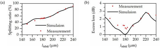
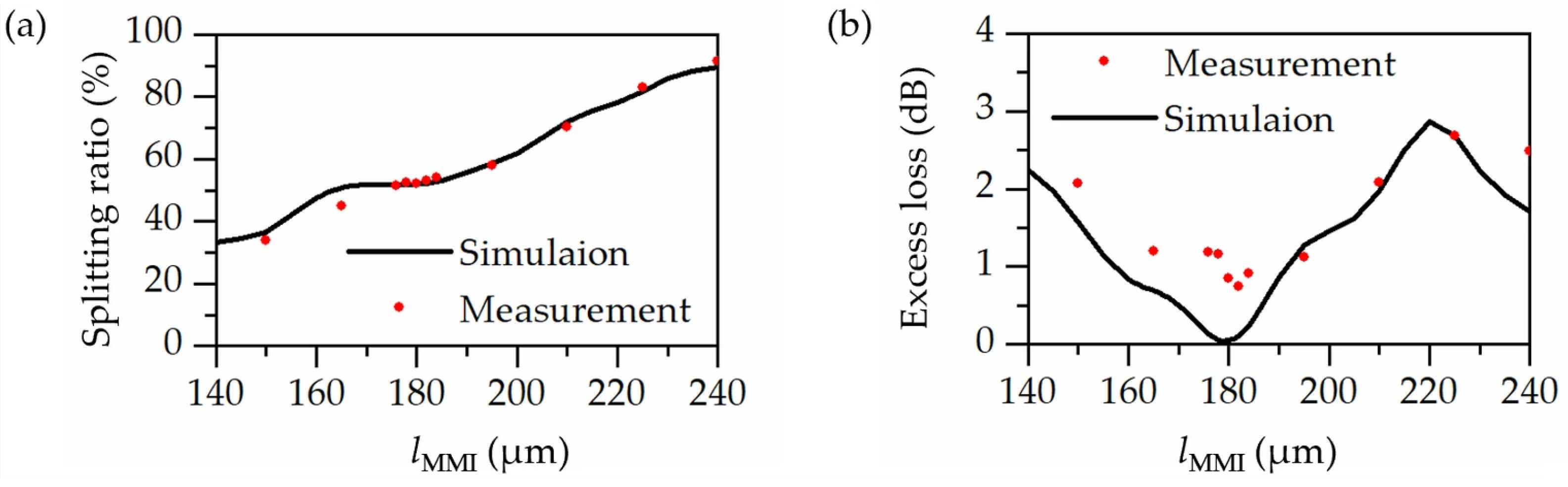
The characteristics of the 2 × 2 MMI coupler were also experimentally investigated. Figure 10 shows the measured and simulated splitting ratios and excess losses as functions of lMMI. A 50:50 splitting ratio was achieved at an lMMI of 178 μm, which is only 1 μm shorter than the simulated optimum. The excess loss also exhibited a dependence on lMMI similar to the simulation results.
Figure 10.
Comparison between simulation and measurement results of the fabricated 2 × 2 MMI coupler. (a) Splitting ratio and (b) excess loss as functions of lMMI. The measured 50:50 splitting ratio was obtained at lMMI = 178 μm, closely matching the simulated optimum length of 179 μm.
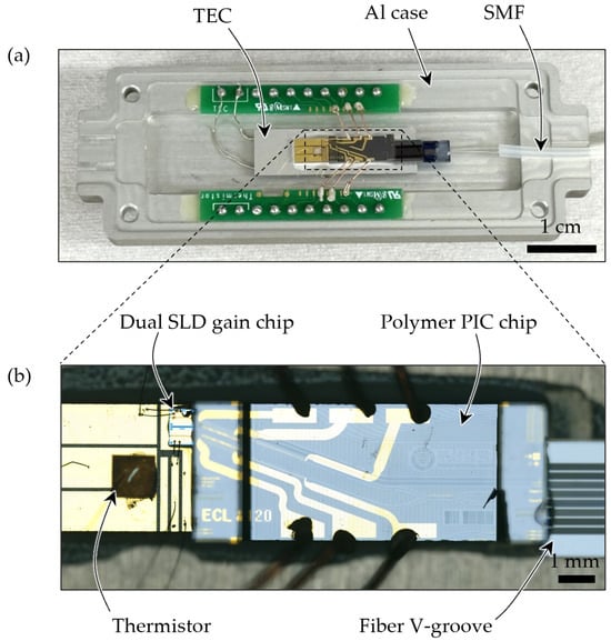
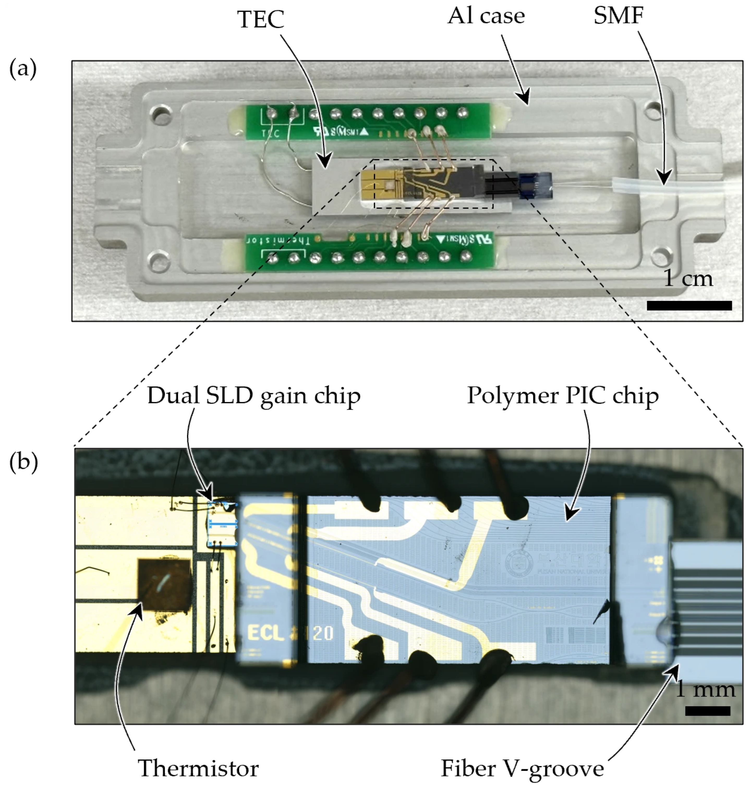
A fiber V-groove was pigtailed to the fabricated polymer PIC for laser output, and the PIC was butt-coupled to an InP-based dual SLD gain chip. An AR coating was applied to the end facet of the gain chip facing the PIC to suppress internal cavity reflections. The gain chip was mounted on an AlN sub-mount with high thermal conductivity for efficient heat transfer. The 2-λ ECL device was packaged in an Al case, as shown in Figure 11. The package includes a TEC and a thermistor, and its temperature was maintained within 0.01 °C using PID control.
Figure 11.
Photograph of the packaged 2-λ ECL. (a) Top view of the device mounted in an aluminum case with TEC control. (b) Enlarged view of the chip region showing the dual SLD gain chip, the polymer PIC chip, the thermistor, and the fiber V-groove.
4. RF Signal Generation Using Optical Heterodyning
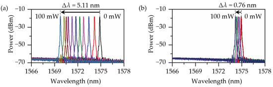
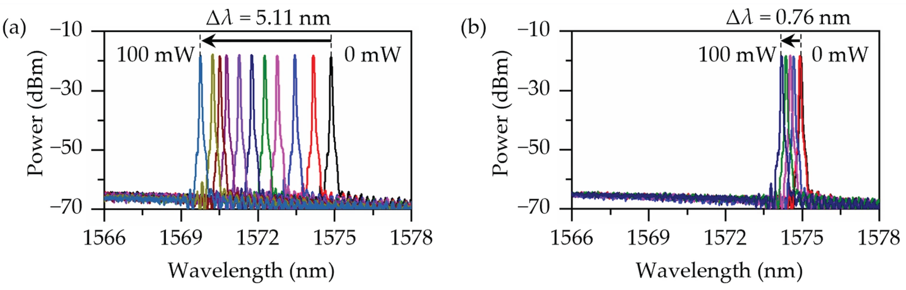
The wavelength tuning characteristics of the fabricated 2-λ ECL were investigated by operating one of the two SLDs, and powers of up to 100 mW were applied to the grating heater and the cavity phase modulator, respectively. The output wavelength shifts were measured as shown in Figure 12. By applying 100 mW to the grating heater, the output wavelength was shifted by −5.11 nm, whereas applying the same power to the cavity phase modulator resulted in a wavelength shift of −0.76 nm. The SMSR of the ECL output was 45.03 dB.
Figure 12.
Wavelengthtuning characteristics of the fabricated 2-λ ECL measured with only one of the two ECLs activated. Powers of up to 100 mW were applied to the TO phase modulators, and the resulting output wavelength shifts are shown for (a) the grating heater and (b) the cavity phase modulator.
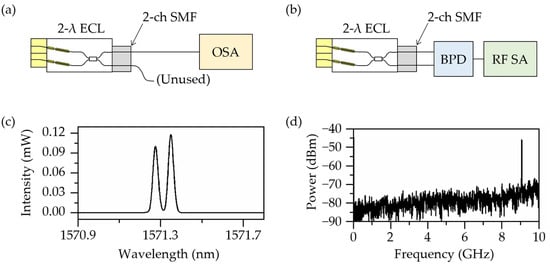
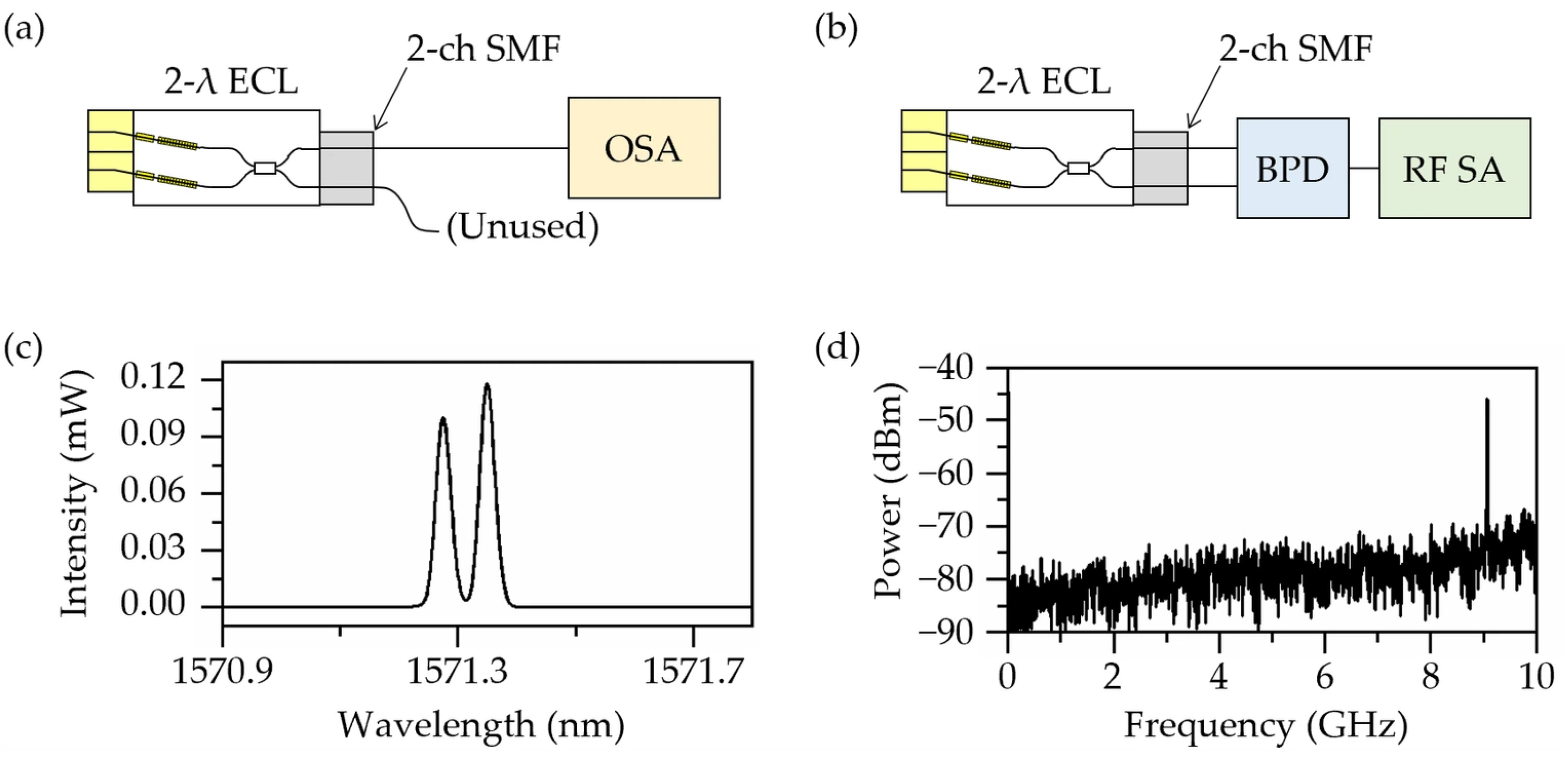
Optical heterodyne RF signal generation was demonstrated by combining the two optical signals with different wavelengths generated by the 2-λ ECL. The experimental setups for optical and RF spectrum measurements are shown in Figure 13a and Figure 13b, respectively. Figure 13c shows the optical output spectrum of the 2-λ ECL with two lasing wavelengths, while Figure 13d shows the corresponding RF spectrum. When the wavelength difference between the two optical signals Δλ is sufficiently smaller than the center wavelength λc, the RF frequency can be approximated as fRF ≈ |cΔλ/λc2|. Using Δλ ≈ 75 pm and λc ≈ 1571 nm obtained from Figure 13c, fRF was calculated to be approximately 9.08 GHz, which is close to the measured RF frequency of 9.07 GHz shown in Figure 13d. The optical spectrum was measured using an Anritsu MS9740B OSA with a wavelength resolution of 0.03 nm, while the RF spectrum was measured using an Anritsu Field Master Pro MS2090A with a resolution bandwidth (RBW) of 10 MHz and a video bandwidth (VBW) of 3.33 MHz. Under free-running operation, the measured RF beat spectral width was 11.22 MHz.
Figure 13.
Experimentaldemonstration of optical heterodyning using the 2-λ ECL. Measurement setups for (a) optical and (b) RF spectra using an optical spectrum analyzer (OSA) and an RF spectrum analyzer (RF SA) with a BPD, respectively. (c) Optical spectrum with a wavelength separation of approximately 75 pm at a center wavelength of approximately 1571 nm, corresponding to a calculated RF frequency of 9.08 GHz. (d) RF spectrum with an RF frequency of 9.07 GHz.
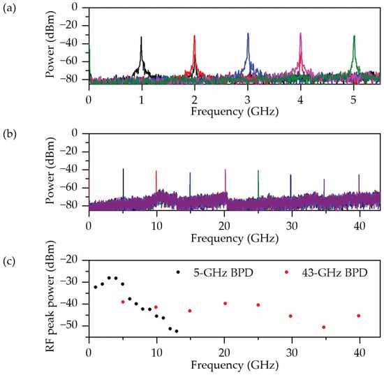
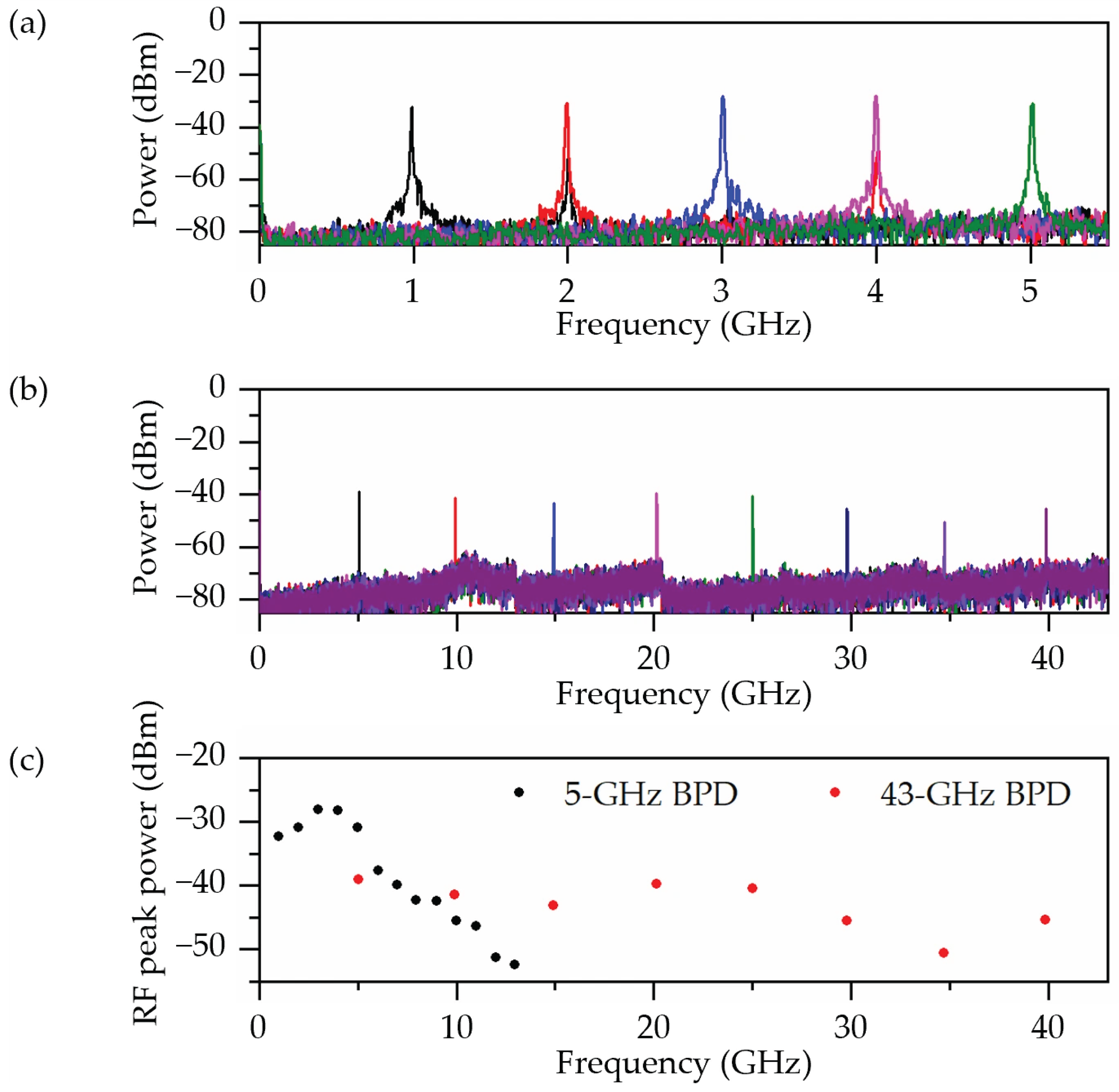
The RF frequency tuning characteristics of the 2-λ ECL were investigated. For the measurements in Figure 14, both SLD gain sections were operated at 60 mA, and the gain chip and polymer PIC were maintained at 25 °C. When operated individually, the total optical output powers from the two MMI ports were −1.21 dBm and −1.36 dBm for the upper and lower ECL channels, respectively. Figure 14a shows the measurement results acquired using a 5-GHz-bandwidth photodetector. Continuous optical wavelength tuning was achieved by Bragg wavelength tuning and cavity mode tuning, and the corresponding RF frequencies are presented at 1-GHz intervals. Despite the free-running operation, distinct RF signals were observed. To investigate higher RF frequencies, a 43-GHz-bandwidth photodetector was employed, and the results are shown in Figure 14b. The RF measurement range was limited to 40 GHz by the RF spectrum analyzer used in the experiment. By tuning the optical wavelengths, RF signals were generated and measured up to this frequency. Figure 14c shows the measured RF peak power as a function of RF frequency. The observed power variation is mainly attributed to the overall frequency response of the RF measurement system, including the BPDs, RF cables, connectors, and RF spectrum analyzer, with a roll-off above 5 GHz for the 5-GHz-bandwidth BPD.
Figure 14.
RF spectraof the generated beat signals were measured using (a) a 5-GHz-bandwidth BPD and (b) a 43-GHz-bandwidth BPD over frequency ranges of 1–5 GHz and 5–40 GHz, respectively. (c) Measured RF peak power as a function of RF frequency for the 5-GHz- and 43-GHz-bandwidth BPDs.
5. Discussion
Table 1 compares the RF characteristics of the proposed 2-λ ECL with those of previously reported dual-wavelength integrated laser sources. The monolithic InP source reported in [35] demonstrated continuous RF tuning from 5 to 110 GHz, whereas hybrid InP/Si and InP/Si3N4 ECLs based on Vernier MRRs provided tuning ranges of several terahertz and narrow linewidths [16,18,19]. A polymer-PIC-based ECL has demonstrated continuous RF tuning over a wide frequency range of up to 1.2 THz [23]. In addition, optical injection locking (OIL) has reduced the RF linewidth from 2.8 MHz under free-running operation to 12 kHz [14] and has also been employed for stabilized RF generation in practical applications [15]. These results support the application of similar stabilization techniques to the proposed 2-λ ECL.
Table 1.
Comparisonof dual-wavelength integrated laser sources for RF generation.
The previously reported polymer/InP 2-λ ECLs employ reverse-operated Y-junctions, which introduce an intrinsic 3 dB combining loss [14,15,23]. In contrast, the 2 × 2 MMI coupler adopted in the present work provides two output ports that can both be utilized, thereby avoiding this intrinsic combining loss. Furthermore, one port can be used for optical injection while the other serves as the output, facilitating the future implementation of OIL.
The RBW-limited RF beat spectral width of 11.22 MHz represents the free-running performance of the two ECLs, and further reduction is required for practical RF/mmWave applications. OIL and an optical phase-locked loop (OPLL) can reduce MHz-level RF beat linewidths to tens of kilohertz, enabling improved carrier phase stability in coherent communications and measurement precision in radar and sensing applications [36,37,38,39]. The integrated 2 × 2 MMI coupler and TO phase modulators provide a suitable architecture for implementing these stabilization techniques to improve the RF linewidth, phase noise, and frequency stability.
6. Conclusions
In this work, we designed and fabricated a 2-λ ECL using a fluorinated polyimide-based polymer PIC and an InP-based dual SLD gain chip. In the proposed polymer PIC, waveguide Bragg gratings, 2 × 2 MMI coupler, and TO phase modulators were integrated, and its structure was designed to combine the outputs of two ECLs on a single chip. The 2-λ ECL was implemented by butt-coupling a dual SLD gain chip to the polymer PIC.
Wavelength tuning characteristics of the fabricated 2-λ ECL were experimentally verified through Bragg wavelength tuning and cavity mode tuning. Optical heterodyning was confirmed by comparing the measured optical wavelengths and the corresponding RF frequency. In addition, RF signals were successfully generated even under free-running operation. Furthermore, continuous RF tuning through optical wavelength control was demonstrated up to the 40 GHz measurement limit of the available RF spectrum analyzer.
The proposed polymer PIC-based 2-λ ECL can be further developed for the integration of RF photonic transceivers on a PIC. Its wide and continuous RF tuning capability makes it well suited for optical-heterodyning-based RF signal sources in radio-over-fiber (RoF) systems, photonic radar, and sensing applications.
Author Contributions
Conceptualization, K.-W.C., E.-S.L., J.J., H.K., G.J.L., S.K. and M.-C.O.; methodology, K.-W.C., E.-S.L., J.J. and M.-C.O.; software, J.J.; validation, G.J.L., S.K. and M.-C.O.; formal analysis, K.-W.C., E.-S.L., J.J., G.J.L., S.K. and M.-C.O.; investigation, K.-W.C., E.-S.L., J.J. and M.-C.O.; resources, G.J.L., S.K. and M.-C.O.; data curation, K.-W.C., E.-S.L., J.J. and M.-C.O.; writing—original draft preparation, K.-W.C., E.-S.L., J.J. and M.-C.O.; writing—review and editing, K.-W.C., E.-S.L., J.J., G.J.L., S.K. and M.-C.O.; visualization, K.-W.C., E.-S.L., J.J. and H.K.; supervision, G.J.L., S.K. and M.-C.O.; project administration, G.J.L., S.K. and M.-C.O.; funding acquisition, G.J.L., S.K. and M.-C.O. All authors have read and agreed to the published version of the manuscript.
Funding
This work was supported by the National Research Foundation of Korea (NRF) funded by the Korean government (MSIT), grant number RS-2026-25493197.
Institutional Review Board Statement
Not applicable.
Informed Consent Statement
Not applicable.
Data Availability Statement
Data is contained within the article.
Conflicts of Interest
The authors declare no conflicts of interest.
Appendix A. Fourier Analysis of the Bragg Grating
In this Appendix, a Fourier-analysis-based design method for waveguide Bragg gratings considering fabrication-induced sidewall rounding is described. The width of the Bragg grating varies periodically along the propagation direction, and this can be expressed by Fourier series as follows [40,41].
Here, z denotes the propagation direction of light, and Cm is the coefficient of the mth-order component in the Fourier expansion. In addition, K = 2π/Λ is the spatial frequency of the grating, and Λ denotes the grating period.
To design the reflection characteristics, the coupling coefficient κ(z) between the forward and backward propagating modes should be considered. κ(z) is determined by the effective refractive index variation Δneff(z) induced by the width variation w(z) along the z-direction. According to coupled mode theory, the reflection amplitude can be expressed as follows.
The reflection amplitude r(λ) in (A2) takes the form of the Fourier transform of κ(z), and because κ(z) is proportional to w(z), the mth Fourier coefficient, Cm, of w(z) directly contributes to the mth-order Bragg reflection amplitude. Here, Δβ(λ) is the detuning parameter, which is defined as follows.
β(λ) is the propagation constant at wavelength λ, and βB,m = mK/2 denotes the propagation constant satisfying the mth-order Bragg condition. According to coupled mode theory, the reflectivity can be expressed as follows [42,43].
Here, κeff is the effective coupling coefficient. The reflectivity of a grating with an ideal rectangular profile can be calculated using the transfer matrix method, and κeff,rec can be extracted from (A4). Using the ratio between the mth Fourier coefficient Cm,ext extracted from the sidewall profile of the test sample and the corresponding coefficient Cm,rec of the ideal rectangular profile, the effective coupling coefficient κeff,ext of the test sample can be calculated as follows.
Therefore, the grating length lg can be adjusted to design a Bragg grating with the target reflectivity.
References
- Leitenstorfer, A.; Moskalenko, A.S.; Kampfrath, T.; Kono, J.; Castro-Camus, E.; Peng, K.; Qureshi, N.; Turchinovich, D.; Tanaka, K.; Markelz, A.G.; et al. The 2023 terahertz science and technology roadmap. J. Phys. D Appl. Phys. 2023, 56, 223001. [Google Scholar] [CrossRef] [Scilit]
- Jornet, J.M.; Petrov, V.; Wang, H.; Popović, Z.; Shakya, D.; Siles, J.V.; Rappaport, T.S. The Evolution of Applications, Hardware Design, and Channel Modeling for Terahertz (THz) Band Communications and Sensing: Ready for 6G? Proc. IEEE 2025, 113, 920–951. [Google Scholar] [CrossRef] [Scilit]
- Nagatsuma, T.; Ducournau, G.; Renaud, C.C. Advances in terahertz communications accelerated by photonics. Nat. Photonics 2016, 10, 371–379. [Google Scholar] [CrossRef] [Scilit]
- Yao, J. Microwave photonic systems. J. Light. Technol. 2022, 40, 6595–6607. [Google Scholar] [CrossRef] [Scilit]
- Capmany, J.; Novak, D. Microwave photonics combines two worlds. Nat. Photon. 2007, 1, 319–330. [Google Scholar] [CrossRef] [Scilit]
- Marpaung, D.; Yao, J.; Capmany, J. Integrated microwave photonics. Nat. Photon. 2019, 13, 80–90. [Google Scholar] [CrossRef] [Scilit]
- Dagli, N. Wide-bandwidth lasers and modulators for RF photonics. IEEE Trans. Microw. Theory Tech. 1999, 47, 1151–1171. [Google Scholar] [CrossRef] [Scilit]
- Zhu, S.; Zhang, Y.; Feng, J.; Wang, Y.; Zhai, K.; Feng, H.; Pun, E.Y.B.; Zhu, N.H.; Wang, C. Integrated lithium niobate photonic millimetre-wave radar. Nat. Photon. 2025, 19, 204–211. [Google Scholar] [CrossRef] [Scilit]
- Kittlaus, E.A.; Eliyahu, D.; Ganji, S.; Williams, S.; Matsko, A.B.; Cooper, K.B.; Forouhar, S. A low-noise photonic heterodyne synthesizer and its application to millimeter-wave radar. Nat. Commun. 2021, 12, 4397. [Google Scholar] [CrossRef] [Scilit]
- Seeds, A.J.; Shams, H.; Fice, M.J.; Renaud, C.C. Terahertz photonics for wireless communications. J. Light. Technol. 2015, 33, 579–587. [Google Scholar] [CrossRef] [Scilit]
- Burla, M.; Cortés, L.; Li, M.; Wang, X.; Chrostowski, L.; Azaña, J. Integrated waveguide Bragg gratings for microwave photonics signal processing. Opt. Express 2013, 21, 25120–25147. [Google Scholar] [CrossRef] [Scilit]
- Zhang, Z.; de Felipe, D.; Katopodis, V.; Groumas, P.; Kouloumentas, C.; Avramopoulos, H.; Dupuy, J.-Y.; Konczykowska, A.; Dede, A.; Beretta, A.; et al. Hybrid photonic integration on a polymer platform. Photonics 2015, 2, 1005–1026. [Google Scholar] [CrossRef] [Scilit]
- Kleinert, M.; de Felipe, D.; Zawadzki, C.; Brinker, W.; Choi, J.H.; Reinke, P.; Happach, M.; Nellen, S.; Möhrle, M.; Bach, H.-G.; et al. Photonic integrated devices and functions on hybrid polymer platform. Proc. SPIE 2017, 10098, 100981A. [Google Scholar] [CrossRef] [Scilit]
- Carpintero, G.; Hisatake, S.; de Felipe, D.; Guzman, R.; Nagatsuma, T.; Keil, N. Wireless data transmission at terahertz carrier waves generated from a hybrid InP–polymer dual tunable DBR laser photonic integrated circuit. Sci. Rep. 2018, 8, 3018. [Google Scholar] [CrossRef] [Scilit]
- Qian, T.; Schuler, B.; Gupta, Y.D.; Deumer, M.; Andrianopoulos, E.; Lyras, N.K.; Kresse, M.; Weigel, M.; Reck, J.; Mihov, K.; et al. Hybrid photonic integrated circuits for wireless transceivers. Photonics 2025, 12, 371. [Google Scholar] [CrossRef] [Scilit]
- Hulme, J.; Kennedy, M.J.; Chao, R.-L.; Liang, L.; Komljenovic, T.; Shi, J.-W.; Szafraniec, B.; Baney, D.; Bowers, J.E. Fully integrated microwave frequency synthesizer on heterogeneous silicon-III/V. Opt. Express 2017, 25, 2422–2431. [Google Scholar] [CrossRef] [Scilit]
- Suzuki, J.; Matsuura, M.; Takabahashi, M.; Suzuki, Y.; Ohata, N. InP/Si integrated laser with high-tolerance-multistep-long-period diffraction grating. In Proceedings of the IEEE 75th Electronic Components and Technology Conference (ECTC), Dallas, TX, USA, 27–30 May 2025; pp. 596–599. [Google Scholar] [CrossRef] [Scilit]
- Mak, J.; van Rees, A.; Lammerink, R.E.M.; Geskus, D.; Fan, Y.; van der Slot, P.J.M.; Roeloffzen, C.G.H.; Boller, K.-J. High spectral purity microwave generation using a dual-frequency hybrid integrated semiconductor-dielectric waveguide laser. OSA Contin. 2021, 4, 2133–2142. [Google Scholar] [CrossRef] [Scilit]
- Guzman, R.; Gonzalez, L.; Zarzuelo, A.; Cesar Cuello, J.; Ali, M.; Visscher, I.; Grootjans, R.; Epping, J.P.; Roeloffzen, C.G.H.; Carpintero, G. Widely tunable RF signal generation using an InP/Si3N4 hybrid integrated dual-wavelength optical heterodyne source. J. Light. Technol. 2021, 39, 7664–7671. [Google Scholar] [CrossRef] [Scilit]
- Heim, D.A.S.; Bose, D.; Liu, K.; Isichenko, A.; Blumenthal, D.J. Hybrid integrated ultra-low linewidth coil stabilized isolator-free widely tunable external cavity laser. Nat. Commun. 2025, 16, 5944. [Google Scholar] [CrossRef] [Scilit]
- Tao, L.; Yang, H.; Liu, J.; Fan, L.; Yang, S. Synthesis and characterization of highly optical transparent and low dielectric constant fluorinated polyimides. Polymer 2009, 50, 6009–6018. [Google Scholar] [CrossRef] [Scilit]
- de Felipe, D.; Zhang, Z.; Brinker, W.; Kleinert, M.; Maese-Novo, A.; Zawadzki, C.; Möhrle, M.; Keil, N. Polymer-based external cavity lasers: Tuning efficiency, reliability, and polarization diversity. IEEE Photonics Technol. Lett. 2014, 26, 1391–1394. [Google Scholar] [CrossRef] [Scilit]
- de Felipe, D.; Happach, M.; Nellen, S.; Brinker, W.; Kleinert, M.; Zawadzki, C.; Möhrle, M.; Keil, N.; Göbel, T.; Petermann, K.; et al. Hybrid polymer/InP dual DBR laser for 1.5 µm continuous-wave terahertz systems. Proc. SPIE 2016, 9747, 974719. [Google Scholar] [CrossRef] [Scilit]
- de Felipe, D.; Kleinert, M.; Zawadzki, C.; Polatynski, A.; Irmscher, G.; Brinker, W.; Möhrle, M.; Bach, H.-G.; Keil, N.; Schell, M. Recent developments in polymer-based photonic components for disruptive capacity upgrade in data centers. J. Light. Technol. 2017, 35, 683–689. [Google Scholar] [CrossRef] [Scilit]
- Xu, Y.; Maier, P.; Blaicher, M.; Dietrich, P.-I.; Marin-Palomo, P.; Hartmann, W.; Bao, Y.; Peng, H.; Billah, M.R.; Singer, S.; et al. Hybrid external-cavity lasers (ECL) using photonic wire bonds as coupling elements. Sci. Rep. 2021, 11, 16426. [Google Scholar] [CrossRef] [Scilit]
- Andrianopoulos, E.; Lyras, N.K.; Tsokos, C.; Qian, T.; Nellen, S.; de Felipe, D.; Groumas, P.; Raptakis, A.; Gounaridis, L.; Keil, N.; et al. Optical generation and transmission of mmWave signals in 5G era: Experimental evaluation paradigm. IEEE Photonics Technol. Lett. 2022, 34, 1011–1014. [Google Scholar] [CrossRef] [Scilit]
- Noh, Y.-O.; Lee, C.-H.; Kim, J.-M.; Hwang, W.-Y.; Won, Y.-H.; Lee, H.-J.; Han, S.-G.; Oh, M.-C. Polymer waveguide variable optical attenuator and its reliability. Opt. Commun. 2004, 242, 533–540. [Google Scholar] [CrossRef] [Scilit]
- Ando, S. Optical properties of fluorinated polyimides and their applications to optical components and waveguide circuits. J. Photopolym. Sci. Technol. 2004, 17, 219–232. [Google Scholar] [CrossRef] [Scilit]
- Kowalczyk, T.C.; Kosc, T.; Singer, K.D.; Cahill, P.A.; Seager, C.H.; Meinhardt, M.B.; Beuhler, A.J.; Wargowski, D.A. Loss mechanisms in polyimide waveguides. J. Appl. Phys. 1994, 76, 2505–2508. [Google Scholar] [CrossRef] [Scilit]
- Lee, E.-S.; Chun, K.-W.; Jin, J.; Oh, M.-C. Frequency response of thermo-optic phase modulators based on fluorinated polyimide polymer waveguide. Polymers 2022, 14, 2186. [Google Scholar] [CrossRef] [Scilit]
- Lee, E.-S.; Chun, K.-W.; Jin, J.; Oh, M.-C. Enhancement of the thermo-optic phase modulation efficiency in silicon nitride waveguides by incorporating an embedded strip within a planar polymer waveguide. Opt. Express 2025, 33, 5099–5107. [Google Scholar] [CrossRef] [Scilit]
- Lee, E.-S.; Chun, K.-W.; Jin, J.; Lee, S.-S.; Oh, M.-C. High-performance optical phased array for LiDARs demonstrated by monolithic integration of polymer and SiN waveguides. Opt. Express 2023, 31, 28112–28121. [Google Scholar] [CrossRef] [Scilit]
- Prakash, D.P.; Scott, D.C.; Fetterman, H.R.; Matloubian, M.; Du, Q.; Wang, W. Integration of polyimide waveguides with traveling-wave phototransistors. IEEE Photonics Technol. Lett. 1997, 9, 800–802. [Google Scholar] [CrossRef] [Scilit]
- Butt, M.A.; Kazanskiy, N.L.; Khonina, S.N. Advances in waveguide Bragg grating structures, platforms, and applications: An up-to-date appraisal. Biosensors 2022, 12, 497. [Google Scholar] [CrossRef] [Scilit]
- Van Dijk, F.; Kervella, G.; Lamponi, M.; Chtioui, M.; Lelarge, F.; Vinet, E.; Robert, Y.; Fice, M.J.; Renaud, C.C.; Jimenez, A.; et al. Integrated InP heterodyne millimeter wave transmitter. IEEE Photonics Technol. Lett. 2014, 26, 965–968. [Google Scholar] [CrossRef] [Scilit]
- Nazarikov, G.; Rommel, S.; Yao, W.; Monroy, I.T. Optical injection locking for generation of tunable low-noise millimeter wave and THz signals. Appl. Sci. 2021, 11, 10185. [Google Scholar] [CrossRef] [Scilit]
- Gonzalez-Guerrero, L.; Guzman, R.; Ali, M.; Zarzuelo, A.; Cesar Cuello, J.; Dass, D.; Browning, C.; Barry, L.; Visscher, I.; Grootjans, R.; et al. Injection locking properties of a dual laser source for mm-wave communications. J. Light. Technol. 2022, 40, 6685–6692. [Google Scholar] [CrossRef] [Scilit]
- Arafin, S.; Simsek, A.; Lu, M.; Rodwell, M.J.; Coldren, L.A. Heterodyne locking of a fully integrated optical phase-locked loop with on-chip modulators. Opt. Lett. 2017, 42, 3745–3748. [Google Scholar] [CrossRef] [Scilit]
- Shen, X.; Costanzo, R.; Singaraju, P.; Blalock, T.N.; Beling, A.; Bowers, S.M. Compact heterogeneously integrated optical phase-locked loop for 10 GHz to 40 GHz optical frequency difference locking. J. Light. Technol. 2024, 42, 2784–2791. [Google Scholar] [CrossRef] [Scilit]
- Parker, M.C.; Walker, S.D. Arrayed waveguide gratings, fiber Bragg gratings, and photonic crystals: An isomorphic Fourier transform light propagation analysis. IEEE J. Sel. Top. Quantum Electron. 2002, 8, 1158–1167. [Google Scholar] [CrossRef]
- Yariv, A. Coupled-mode theory for guided-wave optics. IEEE J. Quantum Electron. 1973, 9, 919–933. [Google Scholar] [CrossRef] [Scilit]
- Othonos, A.; Kalli, K.; Pureur, D.; Mugnier, A. Fibre Bragg gratings. In Wavelength Filters in Fibre Optics; Venghaus, H., Ed.; Springer: Berlin/Heidelberg, Germany, 2006; pp. 189–269. [Google Scholar] [CrossRef] [Scilit]
- Kogelnik, H. Filter response of nonuniform almost-periodic structures. Bell Syst. Tech. J. 1976, 55, 109–126. [Google Scholar] [CrossRef] [Scilit]

Disclaimer/Publisher’s Note: The statements, opinions and data contained in all publications are solely those of the individual author(s) and contributor(s) and not of MDPI and/or the editor(s). MDPI and/or the editor(s) disclaim responsibility for any injury to people or property resulting from any ideas, methods, instructions or products referred to in the content. |
© 2026 by the authors. Licensee MDPI, Basel, Switzerland. This article is an open access article distributed under the terms and conditions of the Creative Commons Attribution (CC BY) license.