


Abstract
A reconfigurable broadband signal channelized reception technique based on parallel Mach–Zehnder modulators (MZMs) is proposed. In the upper branch, the unknown broadband signal is modulated onto the ±1st-order sidebands of a frequency-shifted optical carrier. In the lower branch, N parallel MZMs are employed, with each MZM generating two local oscillator (LO) comb lines, which beat with the broadband signal from the upper branch to produce 4N sub-channels. By adjusting the frequency shift of the acousto-optic frequency shifter (AOFS) and the frequency of the LO signals, the system achieves tunability over an operating frequency band of 8 to 40 GHz, enabling simultaneous tuning of the sub-channel bandwidth, the number of sub-channels, and their center frequencies. Simulation experiments show that this technique can down-convert a wideband signal with a frequency band of 12–16 GHz to eight intermediate frequency (IF) signals with eight center frequencies of 0.5 GHz and a bandwidth of 0.5 GHz and down-convert a wideband signal with a frequency band of 32–40 GHz to eight IF signals with eight center frequencies of 1 GHz and a bandwidth of 1 GHz, and the image rejection ratio (IRR) is greater than 26 dB, the passband power fluctuation is less than 0.5 dB, and the spurious-free dynamic range (SFDR) is 95.17 dB·Hz2/3.
1. Introduction
In electronic warfare, electromagnetic waves are typically utilized to carry out various military activities such as communication, navigation, positioning, reconnaissance and surveillance [1,2]. In the context of an increasingly complex electromagnetic environment, a channelized receiver with wideband instantaneous coverage, capable of simultaneously receiving, processing and demodulating multiple signals and having a good dynamic range, can effectively receive broadband radio frequency signals [3]. Compared to traditional channelized receivers, channelized receivers based on microwave optics can process microwave signals in the optical domain. They not only have the advantages of large instantaneous bandwidth and low loss but also possess the advantages of strong parallel processing capabilities and resistance to electromagnetic interference [4,5].
Currently, the channelization receiving technology based on comb-like light sources can be classified into two types. The first type modulates the signal to be measured onto the comb-like light source to achieve signal multicast. Then, using an optical filter with a periodic frequency response that is slightly different from the free spectral range (FSR) and the spacing of the comb-like lines, the optical signals of different sub-channels can be separated from the multicast signal, and then the narrowband radio frequency (RF) signals of different sub-channels can be obtained through demultiplexer (De-mux) and photoelectric conversion [6,7,8,9,10,11]. However, the channelization scheme based on a single optical frequency comb (OFC) and periodic filters has requirements for the filter to be narrowband, flat-topped, and with steep edges, and the requirements for the filter are relatively high [12,13].
The second type uses one OFC as the signal OFC to modulate the RF signal and the other OFC as the local oscillator (LO) OFC. Together with the modulated optical signal from the first path, they are input into the coherent receiver for coherent beat frequency. Through the in-phase/quadrature (I/Q) coherent demodulation module composed of an optical hybrid and a photodetector, the modulated RF signal is down-converted. After linear demodulation, narrowband sub-channels can be obtained [14,15,16,17]. In reference [18], the two OFCs in the LO OFC are subjected to left and right frequency shifts by an acousto-optic frequency shifter (AOFS), and together with the signal, they enter the image suppression mixer. Finally, the 6 GHz RF signal is divided into six sub-channels with a bandwidth of 1 GHz, achieving parallel reception; however, the measurement range of this scheme cannot be tuned and struggles to meet the measurement requirements for signals with larger bandwidths. In reference [19], only N + 1 signal OFCs and N LO OFCs are used to generate 4N channels. In the experiment, a four-wire signal OFC and a three-wire LO OFC are used to divide the 2–14 GHz wideband signal into 12 sub-channels with a bandwidth of 1 GHz. However, when channelizing broadband signals of different frequency ranges, this scheme requires redesigning the number and spacing of the comb teeth of the OFC. In reference [20], the AOFS is used to frequency shift the OFC to obtain three times the number of sub-channels of the OFC grating line. In the experiment, a three-wire OFC is used to obtain nine different frequencies of LO signals through left and right frequency shifts, achieving simultaneous reception of 18 sub-channels. In reference [21], a microwave photonic channelization receiver based on signal polarization multiplexing is proposed. Two different frequency LO OFCs are used to demodulate the RF signal in the orthogonal polarization state. The experiment verifies that this system can simultaneously receive 16 sub-channels with a bandwidth of 1 GHz. However, in references [17,19,21], the scheme involves polarization state adjustment, which is easily affected by temperature changes, resulting in polarization state drift, and requires frequent calibration. In reference [22], a microwave photonic channelization scheme based on OFCs and a dual-output image suppression mixer is proposed. The simulation results show that the RF signal with an instantaneous bandwidth of 8 GHz can be channelized into eight sub-channels with a bandwidth of 1 GHz. The measurement range of this scheme is small, and the actual measurement requirements for wideband signals need to be further expanded. In reference [23], a broadband microwave photonic channelization receiver based on dual OFCs is proposed, and the frequency measurement range can be adjusted by adjusting the frequency of f0. However, in references [16,20,23], the scheme not only requires generating a flat OFC but also the working frequency band is limited by the spacing of the OFC; even in reference [23], the measurement frequency range can be adjusted, but the working frequency band is still limited by the spacing of the OFC. Reference [24] proposed a broadband reconfigurable instantaneous microwave multifrequency measurement system based on non-uniform OFCs. By using sawtooth wave modulation to generate 2l + 1 rows of non-uniform OFCs, it can measure the frequencies of multifrequency microwave signals within a wide frequency band of 0.01–102 GHz. Although the system has a wider measurement range, it is unable to measure the frequencies of broadband signals.
In parallel to the above system-level approaches, recent advances in integrated microwave photonics have enabled compact channelized receivers. Reference [25] presents an integrated silicon photonics multichannel optical hybrid device for broadband parallel coherent reception. Its average spurious-free dynamic range (SFDR) reaches 80.8 dB/Hz2/3, and the average image rejection ratio (IRR) is 33.26 dB. Reference [26] proposed a reconfigurable microwave photonic channelized receiver chip based on coupled-resonator optical waveguide filter arrays, enabling dynamic bandwidth reconfiguration from 2.25 GHz to 3.12 GHz. These works represent the cutting-edge trend towards high-density integration and scalability that is critical for the future adoption of microwave photonic sub-systems. Compared with these integrated solutions, our parallel-MZM-based architecture offers a wider operating frequency range and enables system reconfigurability without requiring complex filter arrays or high-order optical filters.
In this paper, a reconfigurable wideband signal channelization receiving technology based on parallel MZMs is proposed. In the upper branch, the optical signal is input into an AOFS to perform a frequency shift of ∆f. The frequency-shifted signal is then input into an MZM0 for carrier-suppressed double-sideband (CS-DSB) modulation, modulating the wideband signal to be measured onto the ±1st sidebands. The two sidebands are separated by a De-mux. In the lower branch, the optical signal is input into N MZMs, and N different frequency RF signals are loaded into the N MZMs to achieve CS-DSB modulation and are mixed with the ±1st sideband modulated wideband signal separated by the De-mux in the upper path to receive the wideband signal. The measurement range, reconfigurability, image rejection, channel equalization, and dynamic range of this method are verified through simulation experiments. The spectral bandwidth used within the working frequency band of 8–40 GHz is calculated to be 80 GHz, with a relatively high spectral utilization rate.
2. Theoretical Analysis
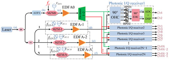
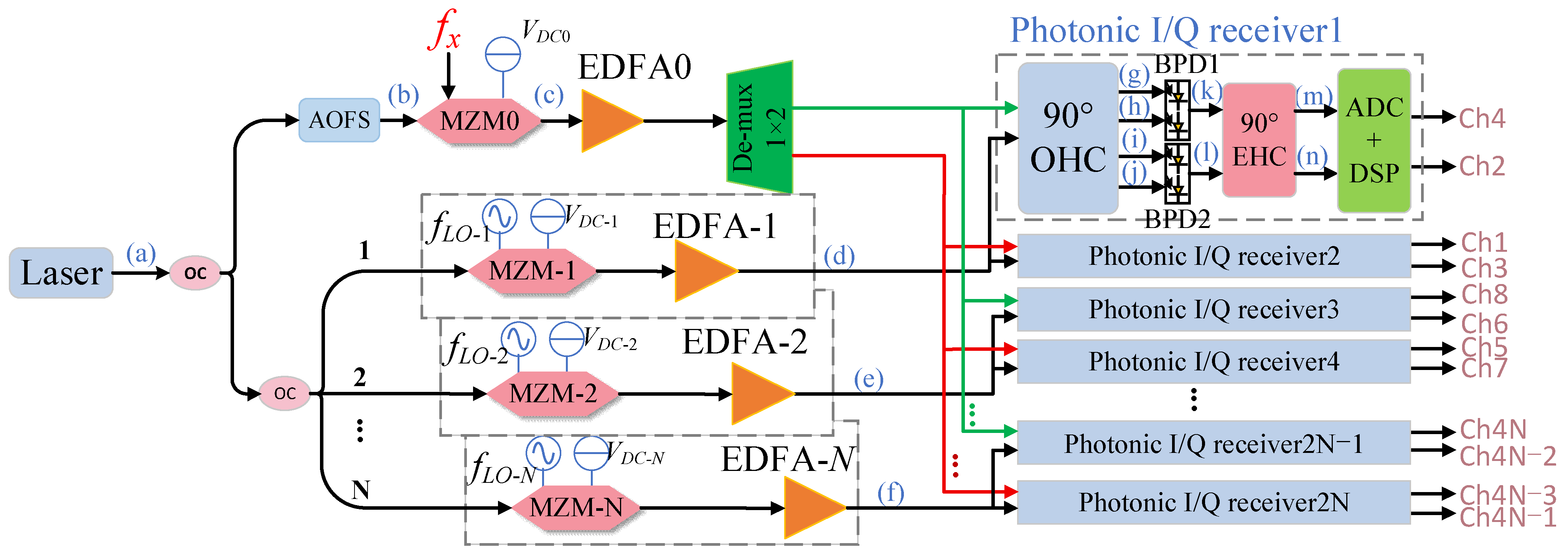
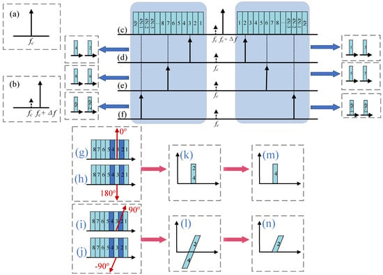
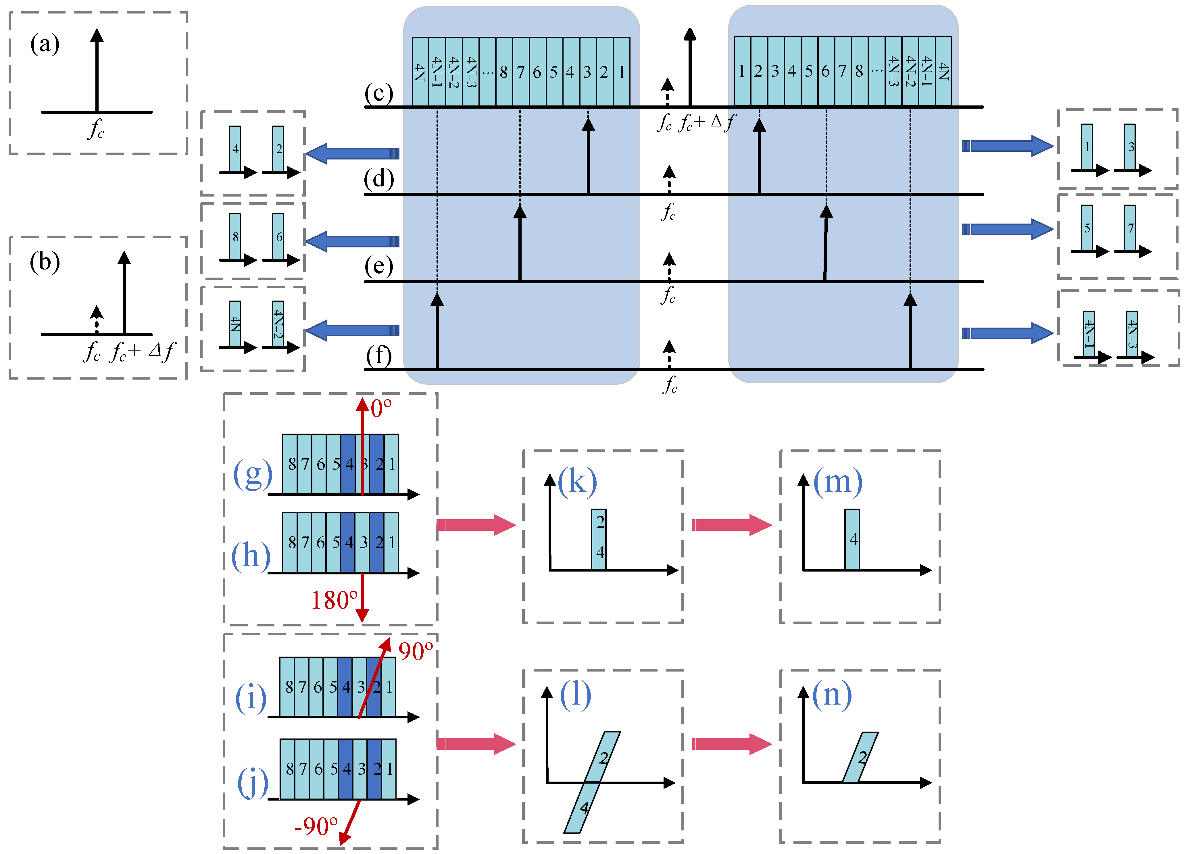
The schematic diagram of this scheme is shown in Figure 1. The continuous laser emits an optical carrier, whose spectrum is shown in Figure 2a. Subsequently, it is input into a 1 × 2 optical coupler (OC) and split into two paths, the upper and lower. In the upper path, the optical carrier is input into an AOFS for frequency shifting, as shown in Figure 2b. The frequency-shifted optical carrier is then input into the MZM0 to achieve CS-DSB modulation, modulating the received wideband signal onto the ±1st-order edges of the shifted optical carrier, as shown in Figure 2c. The modulated signal is amplified by the erbium-doped optical fiber amplifier0 (EDFA0) and then input into the De-mux to separate the two sidebands. In the lower path, the optical carrier first passes through a 1 × N OC to be divided into N paths and is then input into N MZMs. The different frequency LO signals of N paths are respectively loaded onto N MZMs to achieve the LO signal’s CS-DSB modulation, as shown in Figure 2d–f. The upper path’s separated upper and lower sideband wideband signals are respectively combined with the LO optical comb of each branch and then input into the photonic I/Q receiver for beat frequency conversion. The photonic I/Q receiver consists of a 90° optical hybrid coupler (OHC), two balanced photodetectors (BPDs) and a 90° electrical hybrid coupler (EHC). After photoelectric detection by the photonic I/Q receiver, the intermediate frequency (IF) signal is output. Finally, an analog-to-digital converter (ADC) and a digital signal processor (DSP) are used for I/Q amplitude and phase imbalance compensation, as well as for digital domain bandpass filtering to restore the signal of each sub-channel. The specific principle analysis is as follows.
Figure 1.
System schematic diagram.
Figure 2.
Spectra diagrams at each point of the system (a) Output optical spectrum of the optical carrier. (b) Output optical spectrum of the optical carrier after passing through the AOFS. (c) Optical spectrum of the broadband signal after being modulated into the optical domain by MZM0. (d–f) Output spectra after different LO signals are modulated by the MZM. (g–j) Four-channel optical hybrid signals output by the 90° OHC. (k,l) Electrical spectra output by BPD1 and BPD2, respectively. (m,n) Two optical signals output after passing through the 90° EHC.
Let the optical carrier output by continuous wave (CW) laser be
In Equation (1), Ec and fc represent the amplitude and frequency of the optical carrier,
Subsequently, the optical carrier is input into a 1 × 2 OC and split into two branches, one for the upper path and the other for the lower path. Then the optical signals from the upper and lower paths can be respectively expressed as
The optical carrier signal from the upper branch is input into the AOFS and undergoes a frequency shift of ∆f, as shown in Figure 2b. The output signal of the AOFS can be expressed as
The frequency-shifted signal is fed into MZM0 for modulation. Let the expression of the received wideband signal be Vx(t) = Vx sin(2πfx t), where Vx and fx represent the amplitude and frequency of the wideband signal respectively. The MZM0 operates at the minimum transmission point (MITP) and performs CS-DSB modulation on the received wideband signal. Under the condition of small signal modulation, the output signal of MZM0 can be expressed as
In Equation (5), m1 = πVx/Vπ represents the modulation index of MZM0. EMZM0,USB(t) = √2/2EcJ1(m1)exp[j2π(fc + ∆f + fx)t], EMZM0,LSB(t) = √2/2EcJ1(m1)exp[j2π(fc + ∆f − fx)t]. The output spectrum is shown in Figure 2c.
From this, it can be known that the output of MZM0 is the received broadband signal that is modulated onto the ±1st-order sidebands of the frequency-shifted optical carrier, which is then amplified by EDFA and input into the De-mux to separate the two sidebands.
The optical carrier on the lower branch is first divided into N paths through a 1 × N OC, and the expression of the signal output from each path is as follows:
The divided optical carriers are respectively input into N MZMs. N different frequency LO signals are respectively loaded onto N MZMs. The expression of the LO signal is VN (t) = VLO-N sin (2πf LO-N t), where N is a positive integer, VLO-N and f LO-N represent the amplitude and frequency of the Nth LO signal. If all N MZMs operate in MITP mode, the output of the Nth MZM can be expressed as
In Equation (7), mLO-N = πVLO-N/Vπ represents the modulation index of the Nth MZM. Thus, the lower path achieves CS-DSB modulation for N different LO signals.
In the upper branch, the demultiplexer separates the modulated wideband signal into the upper and lower sidebands. When the upper sideband wideband signal EMZM0,USB(t) separated by the demultiplexer is input into the photonic I/Q receiver together with the local oscillator optical comb from the lower branch, the four optical mixing signals output from the 90° OHC with different phase differences (0°, 180°, 90°, and 270°) in the 2Nth photonic I/Q receiver can be expressed as
Similarly, when the lower sideband wideband signal EMZM0,LSB(t) separated by the demultiplexer is input into the photonic I/Q receiver together with the local oscillator optical comb from the lower branch, the four optical mixing signals output from the 90° OHC with different phase differences (0°, 180°, 90°, and 270°) in the (2N − 1)th photonic I/Q receiver can be expressed as
When the upper band wideband signal EMZM0,USB(t) and the LO optical comb are input together into the photonic I/Q receiver, the four signals output from the 90° OHC are sent to two BPDs for photodetection, and the output I/Q signals can be expressed as
In Equation (9), ℜ represents the responsivity of the BPD.
Since the I/Q signals required by the backend are specific frequency IF signals, the output useful I/Q signals are, respectively,
When there is an image signal fj in the photonic I/Q receiver, ∆f − fj + fLO-N = − fLO-N − ∆f + fx. Since the upper sideband broadband signal output by MZM0 and the +1st sideband signal output by MZM-N undergo beat frequency after being combined and result in an effective signal, therefore, in Equation (13), the lower sideband broadband signal output by MZM0 is not described. Thus, the input signal can be expressed as
After being photoelectrically converted by BPD1 and BPD2, we can obtain
Equations (14) and (15) show that beat frequency down-converts the image and unknown signals to the same intermediate frequency band, thereby causing aliasing, as shown in Figure 2k,l. To prevent overlap, the two signals are fed into a 90° EHC, where one signal (I or Q) is phase-rotated by 90° prior to mixing; the output signals of the EHC’s two sub-channels can be expressed as
From Equations (16) and (17), it can be seen that, after demodulation, the target signal and the image signal can be separated, thus achieving the purpose of image suppression. Based on the detected beat frequency signal fbeat = fLO-N − ∆f − fx = ∆f + fj − fLO-N in the sub-channels of the photonic I/Q receiver output, the frequency of the signal to be measured can be measured as
In the formula, N is an integer, corresponding to the Nth LO signal. For positive integer N, all integers from 1 to N need to be taken. Moreover, 4N − 3 and 4N – 1 correspond to the upper and lower ports of the 2Nth receiver.
By the same reasoning, when the lower band wideband signal EMZM0,LSB(t) and the LO optical comb are input into the photonic I/Q receiver, the output signals of the two sub-channels of the 90° EHC can be represented.
Based on the detected beat frequency signal f beat = −fLO-N − ∆f + fx = ∆f − fj + fLO-N in the sub-channels output by the photonic I/Q receiver, the frequency of the signal to be measured can be determined as
In Equation (21), 4N and 4N − 2 correspond to the upper and lower ports of the (2N − 1)th receiver.
3. Simulation Experiment
3.1. Principle Simulation
According to the system principle block diagram shown in Figure 1, a simulation experiment was conducted using VPI to analyze the performance of this system. In the simulation experiment, since there was no AOFS in VPI, based on its function, the frequency shift module was used to replace AOFS for the frequency shift of ∆f. In the simulation, two LO signals were used to verify the performance of the proposed channelization receiving scheme. The laser relative intensity noise (RIN) is set at −130 dB/Hz, as this value is a typical RIN specification for some commercial narrow-linewidth lasers. The main parameters of the key components are shown in Table 1.
Table 1.
Parameter Settings.
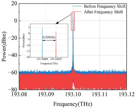
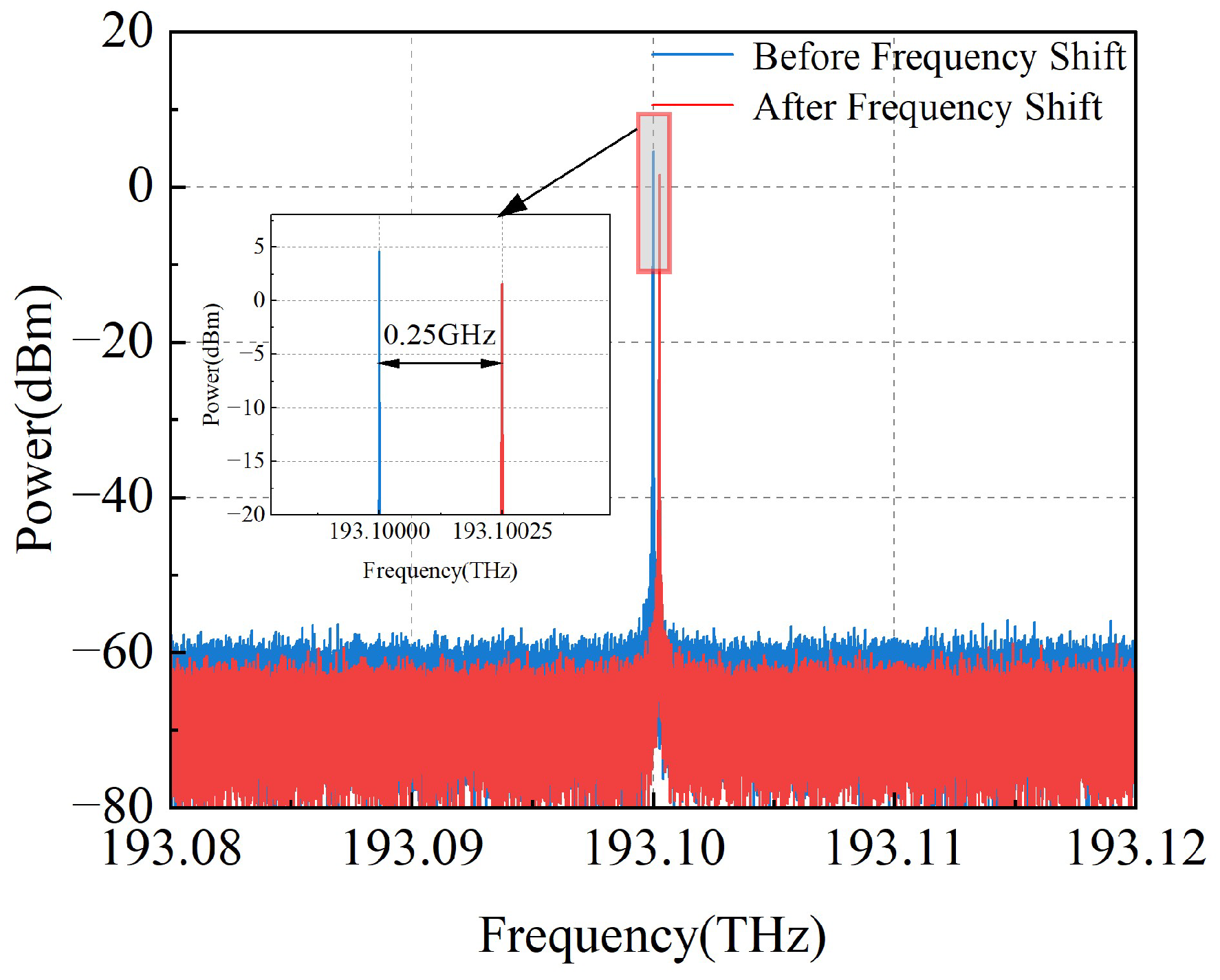
As shown in Figure 3, the optical carrier frequency has been successfully shifted by an amount of Δf = 0.25 GHz. This determines the center frequency and bandwidth of the subsequent sub-channels.
Figure 3.
The optical carrier before and after the AOFS.
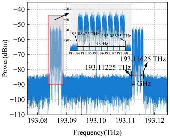
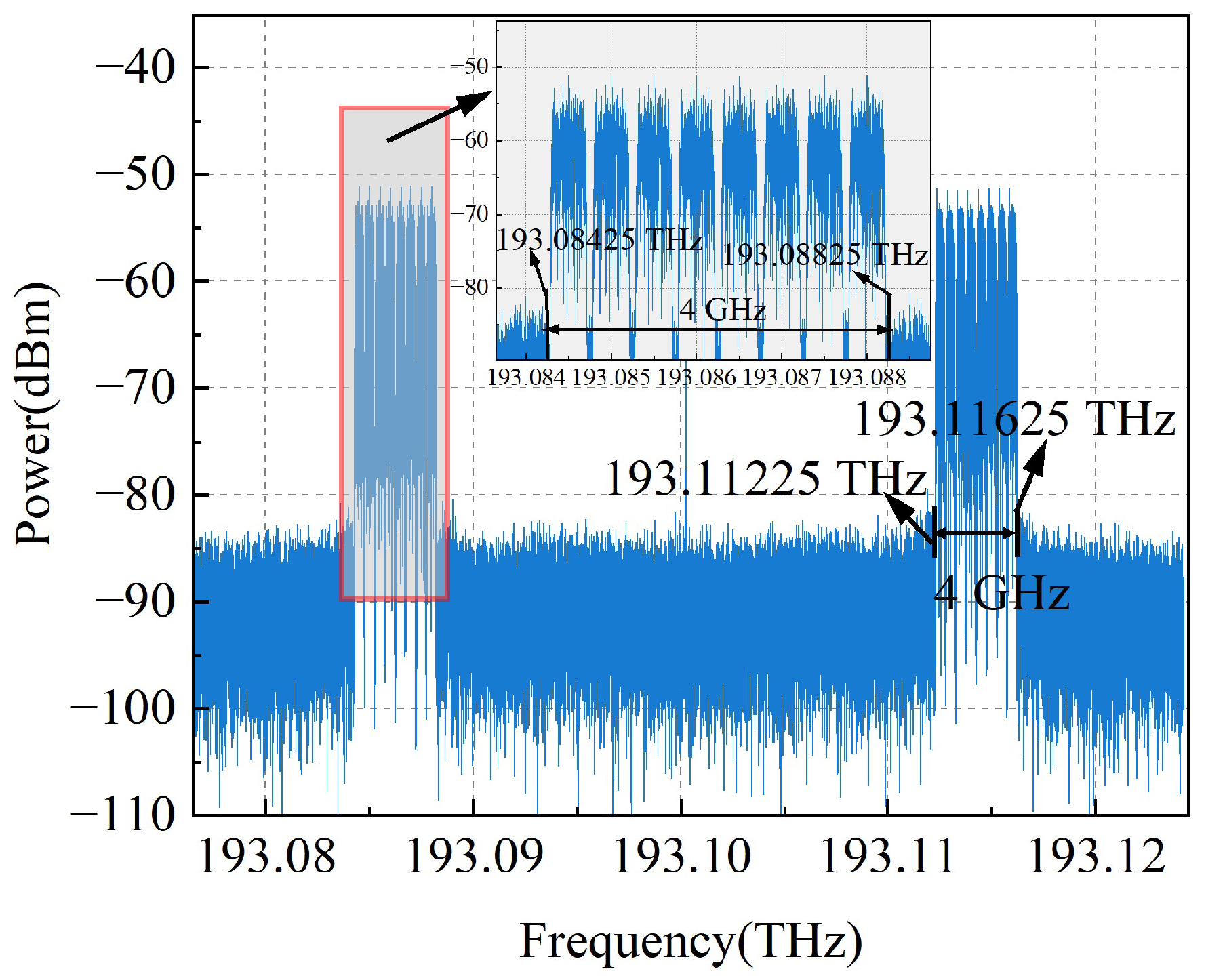
In the simulation, the Symbol Rate was set to 1.5 GHz and the Number of Symbols was set to 2048. The working frequency band of the system was set to 12–16 GHz in the Ku band. The broadband signal generation module concatenated eight signals with a center frequency interval of 0.5 GHz and a bandwidth of 375 MHz each to form a 16-ary quadrature amplitude modulation (16QAM) signal with a total bandwidth of 4 GHz and input it into MZM0 for CS-DSB. The spectrum output by MZM0 is shown in Figure 4.
Figure 4.
Spectrum of the MZM0 Output Signal.
In the lower branch, the optical carrier is divided into two paths via the OC and then input into two MZMs (MZM-1 and MZM-2) for CS-DSB modulation. The frequencies fLO-1 and fLO-2 of the LO signals LO1 and LO2 are set to 13 GHz and 15 GHz respectively, with an amplitude of 1 V. Then, the two LO optical combs output by the two MZMs are shown in Figure 5a,b.
Figure 5.
Output spectra of (a) LO1 and (b) LO2.
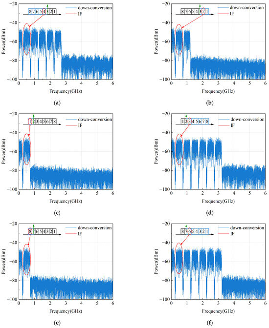
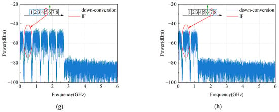
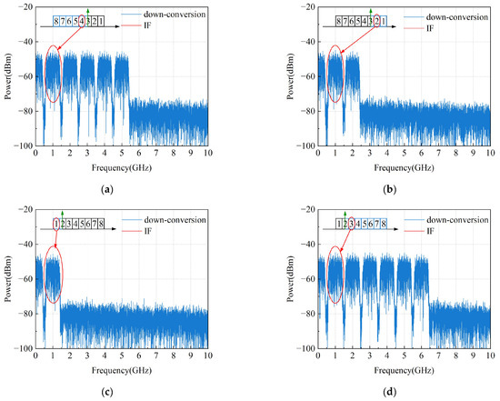
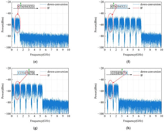
The broadband signal modulated in the upper branch is amplified by an EDFA and then fed into a 1 × 2 De-mux for channel demultiplexing. The bandwidth of the De-mux sub-channels is 4 GHz, with the center frequencies being 193.08625 THz and 193.11425 THz respectively. The lower sideband broadband signal separated by the De-mux are respectively input together with LO1 and LO2 into photonic I/Q receiver 1 and photonic I/Q receiver 3, while the upper sideband broadband signals are respectively input together with LO1 and LO2 into photonic I/Q receiver 2 and photonic I/Q receiver 4. By using the LO optical comb to down-convert the broadband signal, Figure 6 shows the spectrum diagram of the output IF signal. In photonic I/Q receiver 1, as shown in Figure 6a,b, the broadband signals on both sides of LO1 are simultaneously down-converted to IF signals with bandwidths of 2.75 GHz and 1.25 GHz. When the frequency band is set to 0.25–0.75 GHz, substituting fLO-1 = 13 GHz, ∆f = 0.25 GHz and the beat signal fbeat = 0.5 GHz into Equations (21a) and (21b), the center frequencies of Ch4 and Ch2 signals can be calculated as 13.75 GHz and 12.75 GHz respectively. In photonic I/Q receiver 2, as shown in Figure 6c,d, the broadband signals on both sides of LO1 are simultaneously down-converted to IF signals with bandwidths of 0.75 GHz and 3.25 GHz. When the frequency band is set to 0.25–0.75 GHz, substituting fLO-1 = 13 GHz, ∆f = 0.25 GHz and the beat signal fbeat = 0.5 GHz into Equations (18a) and (18b), the center frequencies of Ch1 and Ch3 signals can be calculated as 12.25 GHz and 13.25 GHz respectively.
Figure 6.
Output Spectra of the photonic I/Q receiver. (a) Ch4 in Receiver 1, (b) Ch2 in Receiver 1, (c) Ch1 in Receiver 2, (d) Ch3 in Receiver 2, (e) Ch8 in Receiver 3, (f) Ch6 in Receiver 3, (g) Ch5 in Receiver 4, (h) Ch7 in Receiver 4.
In photonic I/Q receiver 3, as shown in Figure 6e,f, the broadband signals on both sides of the LO1 are simultaneously down-converted to IF signals with bandwidths of 0.75 GHz and 3.25 GHz. When the frequency band is set to 0.25–0.75 GHz for the IF signal, substituting fLO-2 = 15 GHz, ∆f = 0.25 GHz and the beat frequency signal fbeat = 0.5 GHz into Equations (21a) and (21b), the center frequencies of Ch8 and Ch6 signals can be calculated as 15.75 GHz and 14.75 GHz respectively. In photonic I/Q receiver 4, as shown in Figure 6g,h, the broadband signals on both sides of LO2 are simultaneously down-converted to IF signals with bandwidths of 2.75 GHz and 1.25 GHz. When the frequency band is set to 0.25–0.75 GHz for the IF signal, substituting fLO-2 = 15 GHz, ∆f = 0.25 GHz and the beat frequency signal fbeat = 0.5 GHz into Equations (18a) and (18b), the center frequencies of Ch5 and Ch7 signals can be calculated as 14.25 GHz and 15.25 GHz respectively.
Further analysis was conducted on the quality of the demodulated signal. Figure 7 shows the 16QAM signal constellation diagram of the generated eight-channel IF signals and their corresponding error vector magnitude (EVM) values. From the result diagram, it can be seen that this scheme successfully converts a 4 GHz wideband signal channel into eight IF signals with a bandwidth of 0.5 GHz. The EVM values fluctuate between 3.8% and 4.4%, indicating that the demodulated signal has good quality.
Figure 7.
Constellation diagram of the IF signal demodulated by the photonic I/Q receiver. (a) Ch4 in Receiver 1, (b) Ch2 in Receiver 1, (c) Ch1 in Receiver 2, (d) Ch3 in Receiver 2, (e) Ch8 in Receiver 3, (f) Ch6 in Receiver 3, (g) Ch5 in Receiver 4, (h) Ch7 in Receiver 4.
3.2. Reconfigurability Verification
The AOFS frequency shift amount ∆f is changed to 0.5 GHz, then the frequency of the modulated optical carrier after the shift is 193.1005 GHz. The Symbol Rate is changed to 3 GHz, and the working frequency band of the system is set to 32–40 GHz in the Ka band. In the downlink, the frequencies fLO-1 and fLO-2 of the LO signals LO1 and LO2 are changed to 34 GHz and 38 GHz respectively.
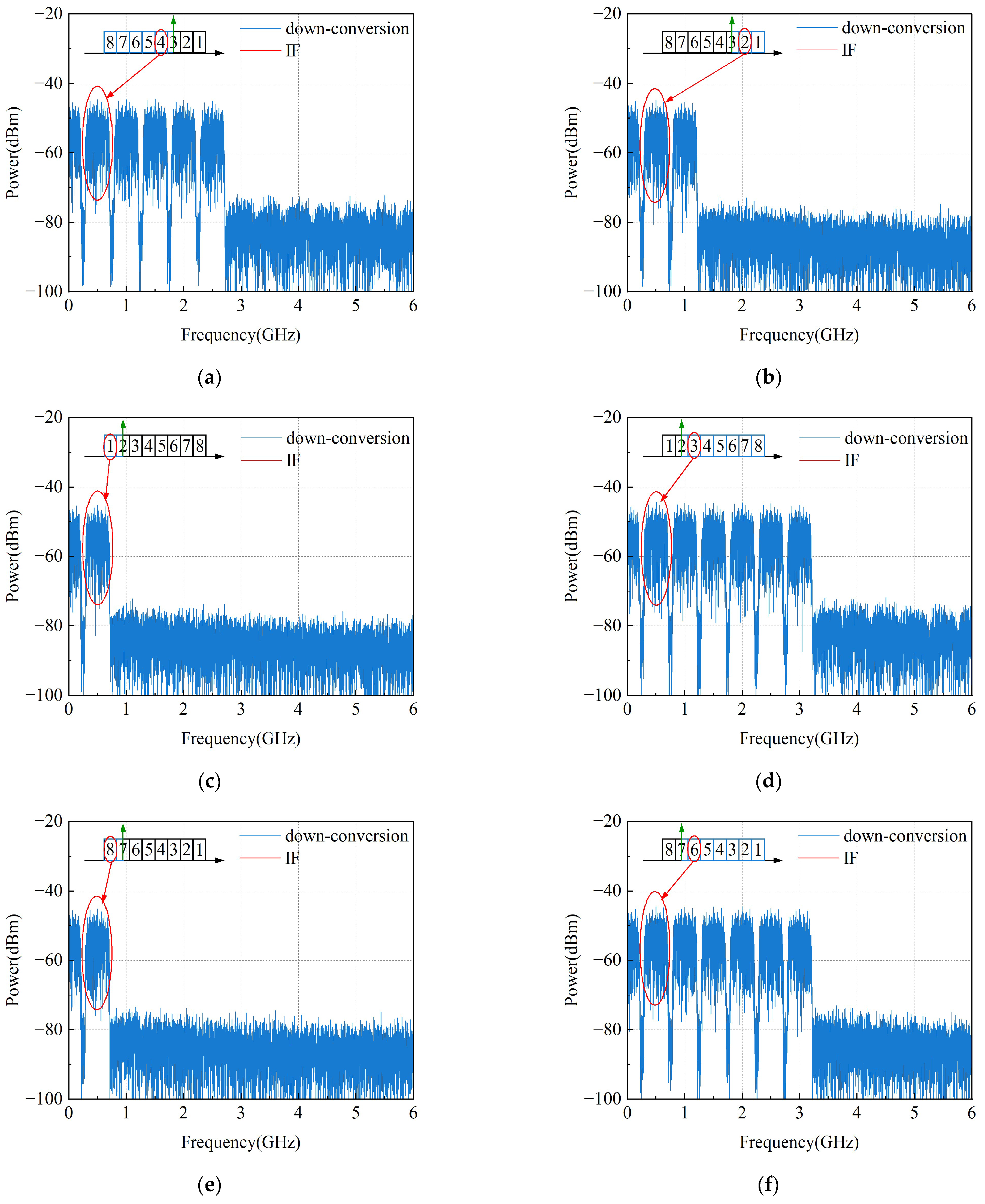
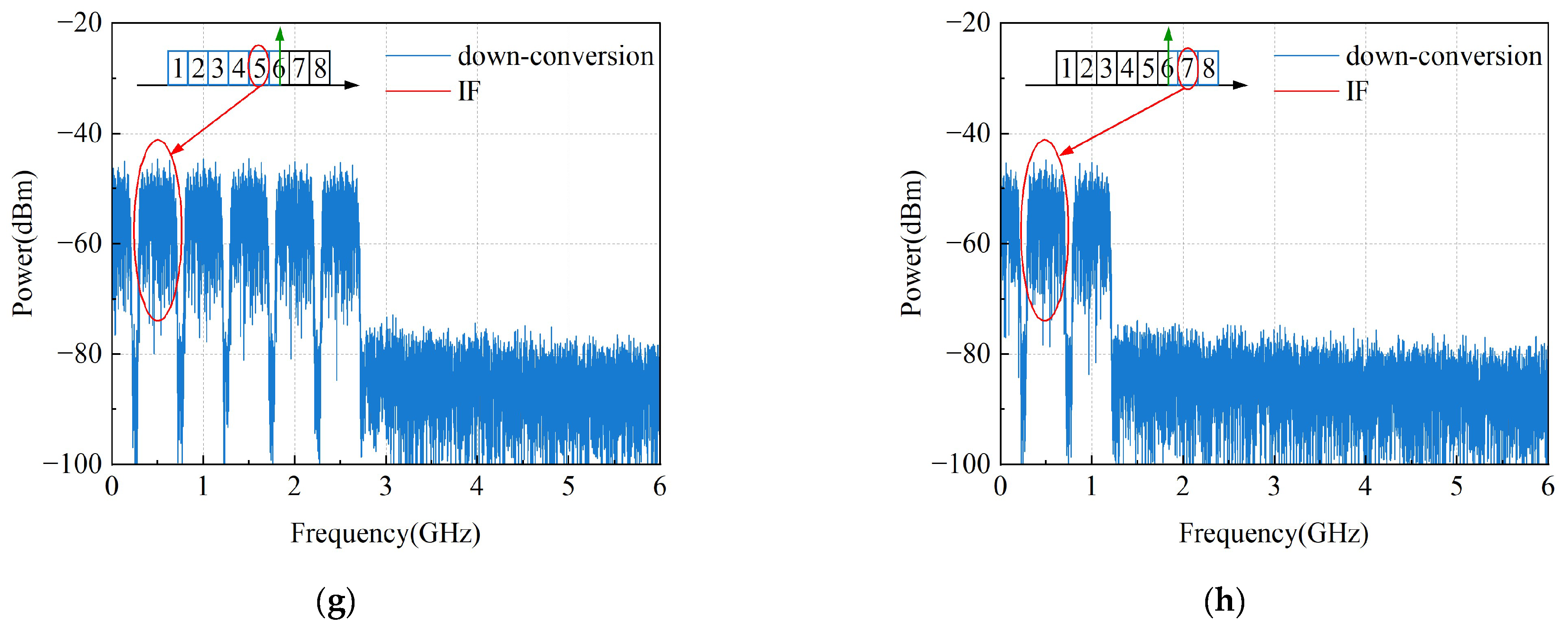
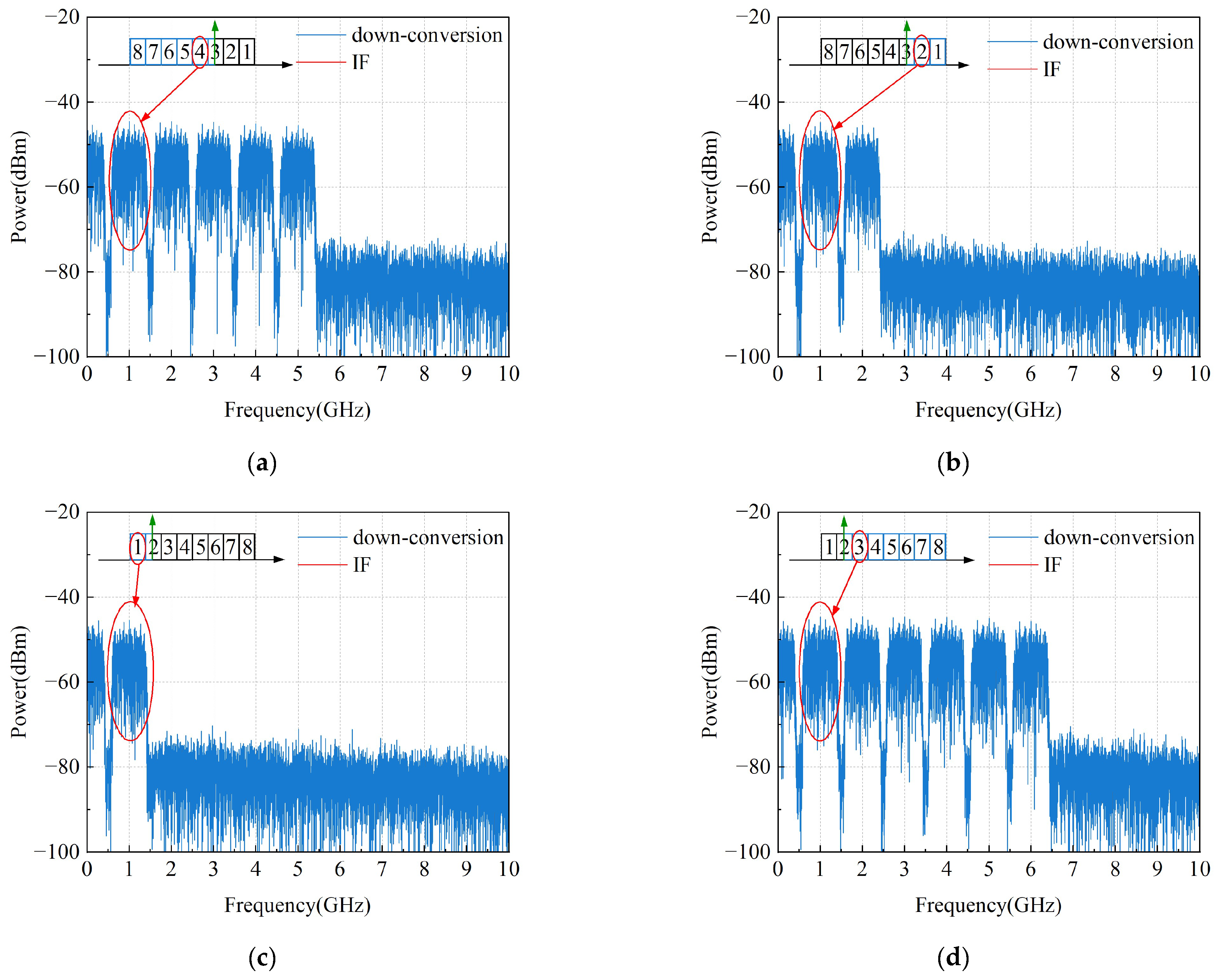
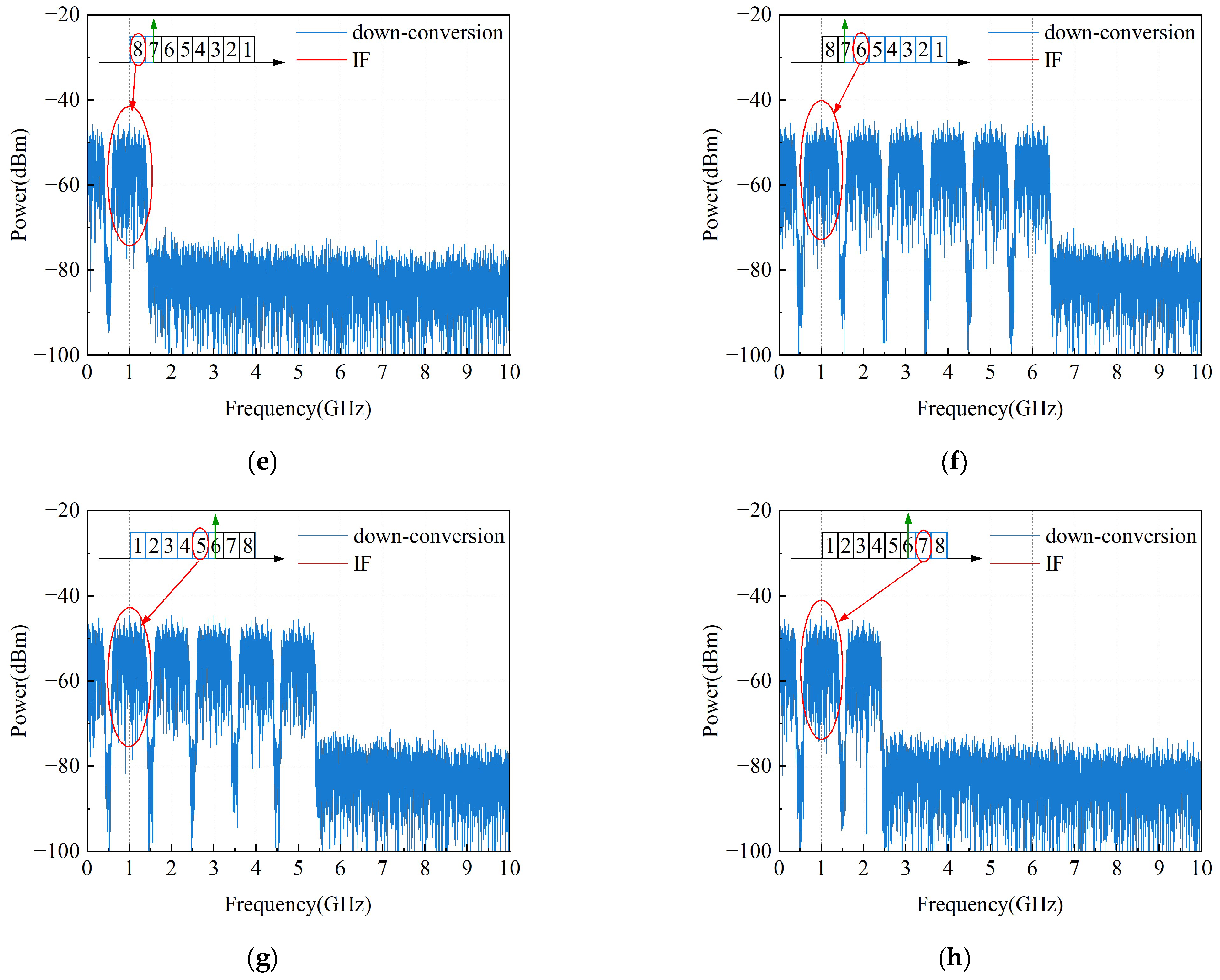
Figure 8 shows the IF spectrogram under the reconfiguration settings. Similar to the previous situation, each photonic I/Q receiver outputs two IF signals with a center frequency of 1 GHz each. By using the updated Δf and LO frequencies and applying Equations (18a)−(21b), the calculated center frequencies of the output sub-channels and the input signal are perfectly consistent. This indicates that the system can seamlessly switch to different frequency bands and sub-channel bandwidths without any hardware modifications, demonstrating the reconfigurability of the system.
Figure 8.
Output Spectra of the photonic I/Q receiver. (a) Ch4 in Receiver 1, (b) Ch2 in Receiver 1, (c) Ch1 in Receiver 2, (d) Ch3 in Receiver 2, (e) Ch8 in Receiver 3, (f) Ch6 in Receiver 3, (g) Ch5 in Receiver 4, (h) Ch7 in Receiver 4.
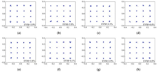
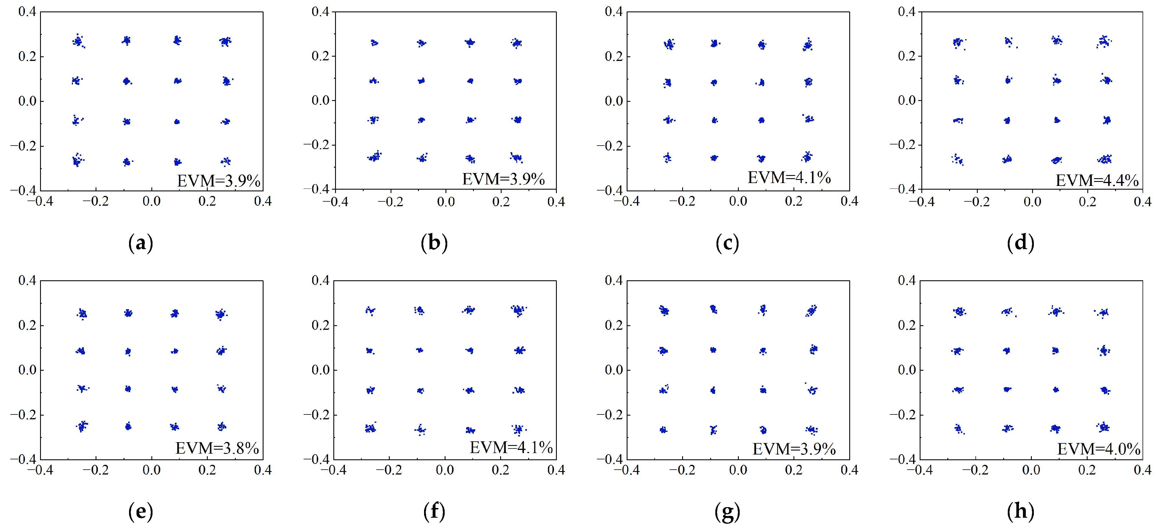
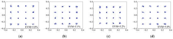
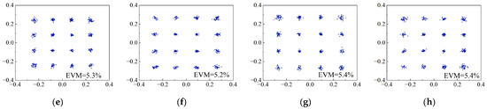
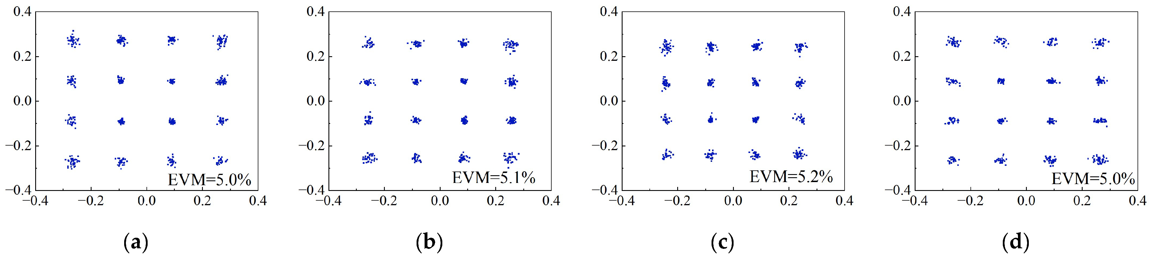
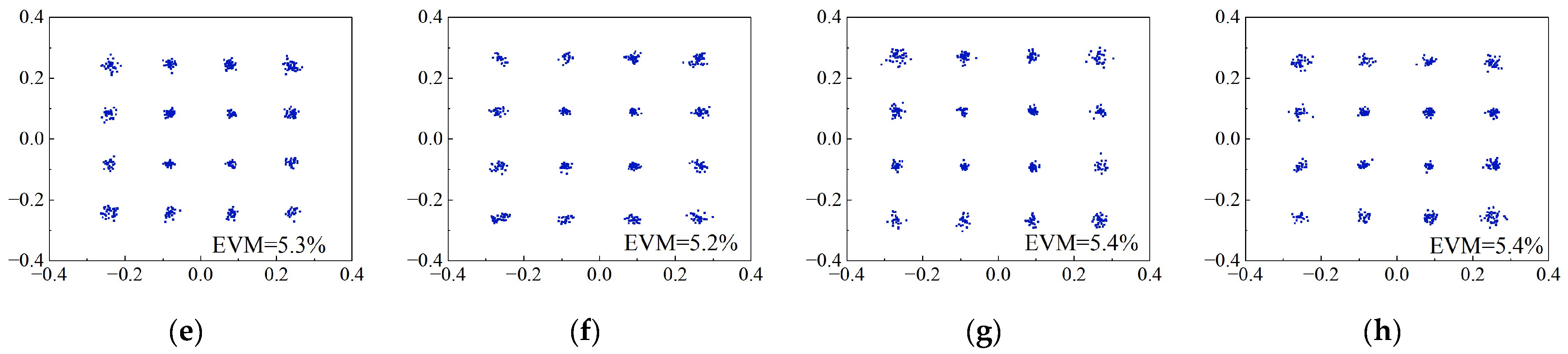
Figure 9 shows the 16QAM signal constellation diagram of the generated eight-channel IF signals and their corresponding EVM values. From the result diagram, it can be seen that this scheme successfully converts the broadband signal channel with a bandwidth of 8 GHz and a frequency range of 32–40 GHz into eight IF signals with a bandwidth of 1 GHz. The EVM values of these signals fluctuate between 5.0% and 5.4%, indicating that the demodulated signals have good quality.
Figure 9.
Constellation diagram of the IF signal demodulated by the photonic I/Q receiver. (a) Ch4 in Receiver 1, (b) Ch2 in Receiver 1, (c) Ch1 in Receiver 2, (d) Ch3 in Receiver 2, (e) Ch8 in Receiver 3, (f) Ch6 in Receiver 3, (g) Ch5 in Receiver 4, (h) Ch7 in Receiver 4.
Compared with the configuration in Section 3.1, this system performs channelization reception for broadband signals in the Ka band (32–40 GHz), with the sub-channel bandwidth being 1 GHz and the sub-channel center frequency being 1 GHz. The number of sub-channels remains at eight. Moreover, the EVM value still stays within the range of 5.0–5.4%, which confirms the reconfigurability of the system. The experimental results confirmed the core advantages of the proposed scheme. When two LO resonator combs with N = 2 generate two sidebands, this system successfully achieves 4N = 8 sub-channels within two frequency bands. By adjusting ∆f and the LO frequency, this system supports simultaneous tuning of sub-channel bandwidth and sub-channel center frequency within the working frequency band of 8–40 GHz.
Increasing the number of MZMs to adjust the number of sub-channels will lead to an increase in the number of system hardware links, raising the complexity of the system. However, in the lower branch, all MZMs operate in exactly the same mode, with highly normalized hardware parameters, significantly reducing the difficulty of debugging and calibration for multiple branches. Meanwhile, the optical paths of the upper and lower branches are independent of each other. Adding a new MZM branch in the lower branch does not require any changes to the core components of the upper branch. Each additional MZM can expand the number of sub-channels by four, enabling an increase in the number of sub-channels at a relatively low cost.
3.3. Image Rejection
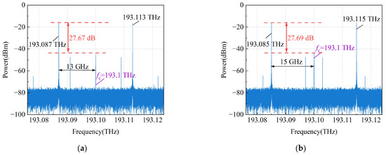
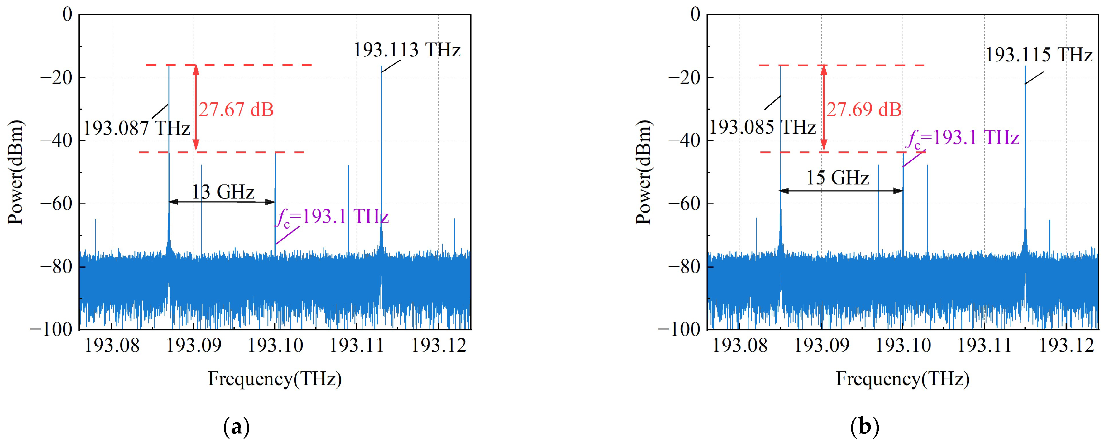
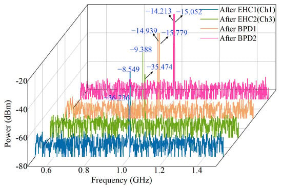
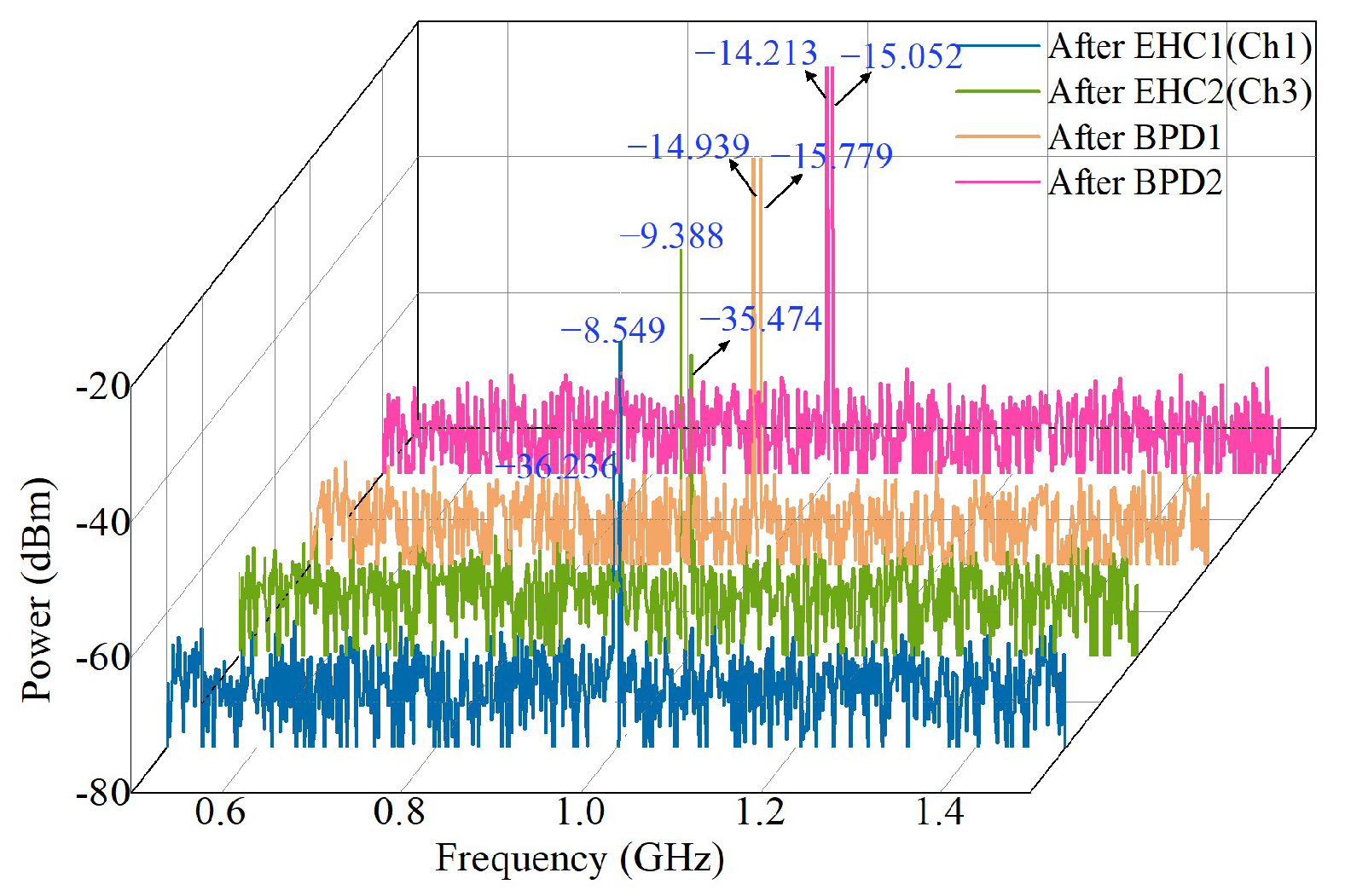
To study the performance of the system’s IRR, RF signals with frequencies of 32.5 GHz and 34.5 GHz were input into the system, respectively located in Ch1 and Ch3 and being image signals to each other. The signals extracted by BPD and 90° EHC are shown in Figure 10. In Figure 10, both signals are down-converted to 1 GHz. The output powers of BPD1 and BPD2 are −14.939 dBm, −15.779 dBm, −14.213 dBm, and −15.052 dBm respectively, with a power difference within 1 dB. After passing through 90° EHC, the frequencies of the two IF signals in Ch1 become −36.236 dBm and −8.549 dBm, and the image rejection ratio of Ch1 is 27.687 dB. The power of the two IF signals in Ch3 becomes −9.388 dBm and −35.474 dBm, and the image rejection ratio of Ch4 is 26.086 dB. Therefore, the I/Q demodulation technique can be utilized to separate the image signals.
Figure 10.
Spectrum of the IF signals output from the BPD and EHC when using RF signals with frequencies of 32.5 GHz and 34.5 GHz.
3.4. Channel Equalization
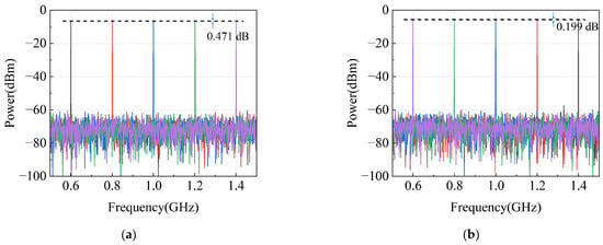
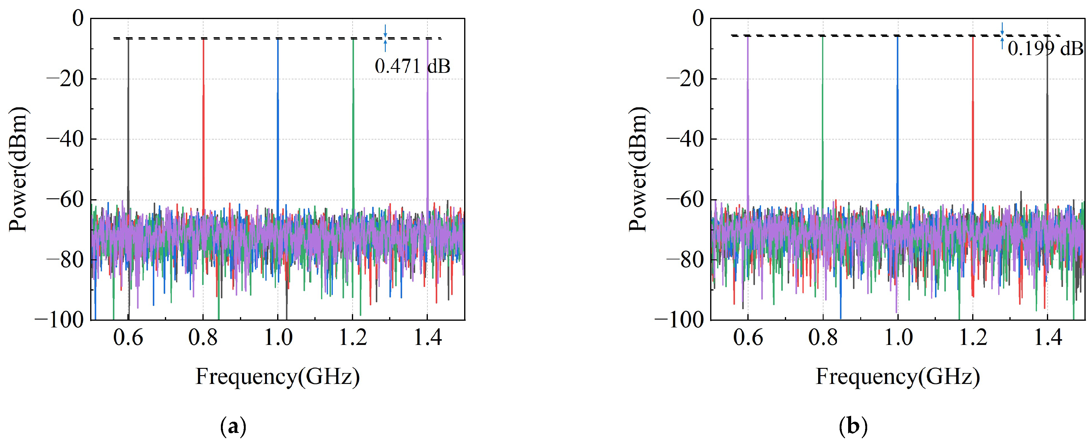
In order to study the channel equalization of the system, a single-frequency signal with an amplitude of 1 V was transmitted at 200 MHz, increasing from 32.1 GHz to 32.9 GHz and from 34.1 GHz to 34.9 GHz respectively. The spectra of the IF signals output from Ch1 and Ch3 of photonic I/Q receiver 2 were measured as shown in Figure 11a,b. From the figures, it can be seen that the input signals were all down-converted to within 0.5–1.5 GHz, and the power fluctuations of different IF signals were less than 0.471 dB, indicating good channel equalization.
Figure 11.
Spectra of the IF signal output from photonic I/Q receiver 2 of (a) Ch1, (b) Ch3.
3.5. Dynamic Range
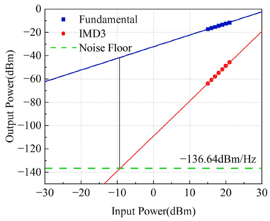
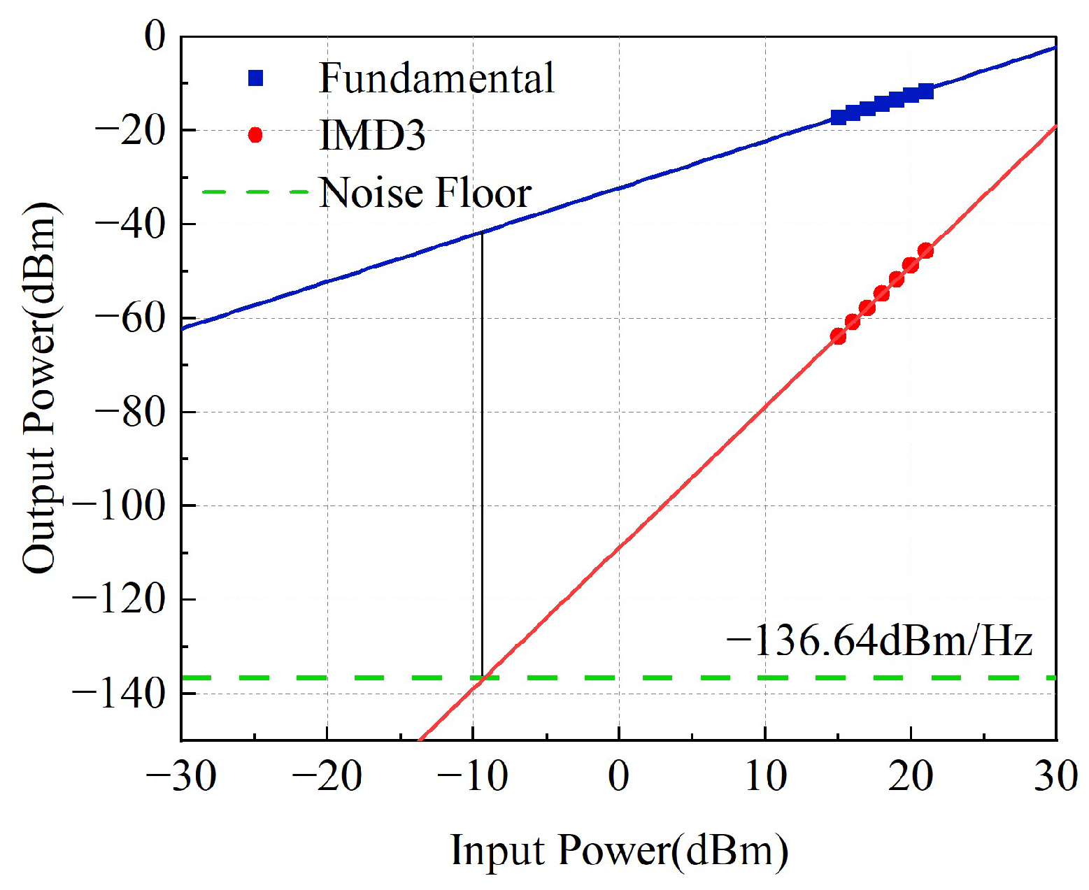
To study the SFDR, while keeping the input LO power unchanged, the SFDR of a channel was measured using a dual-tone signal. When a dual-tone signal with frequencies of 34.49 GHz and 34.51 GHz was loaded on MZM0, the frequencies after down-conversion by the system were 0.99 GHz and 1.01 GHz. When the input signal power was 15 dBm, 16 dBm, 17 dBm, 18 dBm, 19 dBm, 20 dBm, and 21 dBm, the power of the fundamental frequency component and the third-order intermodulation distortion (IMD3) in the output signal was measured. The noise floor of the signal was −136.64 dBm/Hz. From Figure 12, the SFDR of Ch3 can be calculated as 95.17 dB∙Hz2/3.
Figure 12.
The SFDR of the proposed channelizer.
3.6. Comparison of Different Measurement Methods
Furthermore, Table 2 compares the parameters of the recently reported microwave photonic channelization receiving system with the system proposed in this paper. From Table 2, it can be seen that the proposed system has a wider measurement range compared to references [18,19,20,21,22]. Compared to reference [23], although reference [23] has a wider measurement range, the required spectral bandwidth is 200 GHz, and the spectral utilization is relatively low. Therefore, for broadband signal channelization receiving, the proposed system not only has further improvements in the measurement range but also can simultaneously tune the sub-channel bandwidth and the number of sub-channels within the working frequency band and has further improvements in addressing the problem of poor reconfigurability.
Table 2.
Comparison of Different Photon-Assisted Channelization Reception Techniques.
4. Discussion
The proposed reconfigurable wideband signal channelization receiver scheme based on parallel Mach–Zehnder modulators (MZMs) utilizes an acousto-optic frequency shifter (AOFS) combined with carrier-suppressed double-sideband (CS-DSB) modulation in the upper branch and parallel MZMs to generate local oscillator (LO) optical combs in the lower branch. With only N two-comb-line optical combs, 4N sub-channels are generated, achieving simultaneous tuning of sub-channel bandwidth, number, and center frequency over an operating frequency range of 8–40 GHz. Simulation experiments verify successful channelization of wideband signals in the Ku band (12–16 GHz) and the Ka band (32–40 GHz). Compared with existing schemes listed in Table 2, the proposed scheme achieves a favorable balance among wide frequency coverage, spectral efficiency, and reconfigurability, while avoiding the shortcomings of traditional schemes that rely on complex filter arrays, polarization control, or low spectral efficiency. In comparison with recent schemes, Refs. [18,19,20,21,22] exhibit narrow operating bandwidths and relatively fixed sub-channel parameters, making them struggle to adapt to rapidly changing electromagnetic environments. Moreover, Refs. [19,21] employ polarization division multiplexing, which suffers from polarization state drift and requires frequent calibration, thus preventing long-term stable operation. Ref. [23], although offering a tunable wide operating band, can only measure wideband signals with a single-shot bandwidth of 8 GHz, with fixed sub-channel bandwidth and number; moreover, it occupies a large amount of spectral bandwidth because the wideband signal must be multicast onto each signal optical comb line. Refs. [25,26] achieve high integration density but require complex filter arrays. Our scheme focuses on system reconfigurability based on a parallel MZM architecture, maintaining a wide operating band while avoiding the use of complex optical frequency combs. The simultaneous tuning of sub-channel bandwidth, number, and center frequency provides a new solution for wideband signal channelization reception.
5. Conclusions
A broadband reconfigurable channelization receiving scheme based on parallel MZMs is proposed. The core idea is that, by using only N LO signals, each generating two LO optical combs, 4N sub-channels can be generated, thereby achieving efficient spectrum utilization within the working frequency band of 8–40 GHz with a required spectral bandwidth of only 80 GHz. Based on this, by adjusting the frequency shift ∆f of the acousto-optic frequency shifter and the frequency of the LO signals, the system can simultaneously tune the sub-channel bandwidth, the number of sub-channels, and the center frequency of the sub-channels, demonstrating excellent reconfigurability. Additionally, the system employs a photonic I/Q receiver, achieving an image rejection ratio greater than 26 dB, a passband power fluctuation of less than 0.5 dB, and a distortion-free dynamic range of 95.17 dB∙Hz2/3.
Author Contributions
All authors contributed in varying degrees to this paper. Writing—original draft, P.L.; writing—review and editing, M.H.; data curation, J.Z.; visualization, D.M.; supervision, Y.L. All authors have read and agreed to the published version of the manuscript.
Funding
This work was supported in part by the National Natural Science Foundation of China under Grant 62465012 and in part by Yunnan High Level Science and Technology Talents and Innovation Team Selection Special Project under Grant 202405AS350001.
Institutional Review Board Statement
Not applicable.
Informed Consent Statement
Not applicable.
Data Availability Statement
Data underlying the results presented in this paper are not publicly available at this time but may be obtained from the authors upon reasonable request.
Conflicts of Interest
The authors declare no conflicts of interest.
References
- Yang, J.; Li, S.; Xiao, X.; Wu, D.; Xue, X.; Zheng, X. Broadband photonic ADC for microwave photonics-based radar receiver. Chin. Opt. Lett. 2018, 16, 060605. [Google Scholar] [CrossRef] [Scilit]
- Yao, J. Microwave photonic systems. J. Light. Technol. 2022, 40, 6595–6607. [Google Scholar] [CrossRef] [Scilit]
- Xu, W.; Zhu, D.; Pan, S. Coherent photonic radio frequency channelization based on dual coherent optical frequency combs and stimulated Brillouin scattering. Opt. Eng. 2016, 55, 046106. [Google Scholar] [CrossRef] [Scilit]
- Xie, X.; Dai, Y.; Xu, K.; Niu, J.; Wang, R.; Yan, L.; Lin, J. Broadband photonic RF channelization based on coherent optical frequency combs and I/Q demodulators. IEEE Photonics J. 2012, 4, 1196–1202. [Google Scholar]
- Minasian, R.A.; Chan, E.H.W.; Yi, X. Microwave photonic signal processing. Opt. Express 2013, 21, 22918–22936. [Google Scholar] [CrossRef] [Scilit]
- Li, Z.; Zhang, X.; Chi, H.; Zheng, S.; Jin, X.; Yao, J. A reconfigurable microwave photonic channelized receiver based on dense wavelength division multiplexing using an optical comb. Opt. Commun. 2012, 285, 2311–2315. [Google Scholar] [CrossRef] [Scilit]
- Zou, X.; Li, W.; Pan, W.; Yan, L.; Yao, J. Photonic-assisted microwave channelizer with improved channel characteristics based on spectrum-controlled stimulated Brillouin scattering. IEEE Trans. Microw. Theory Tech. 2013, 61, 3470–3478. [Google Scholar] [CrossRef] [Scilit]
- Huang, H.; Zhang, C.; Zhou, H.; Yang, H.; Yuan, W.; Qiu, K. Double-efficiency photonic channelization enabling optical carrier power suppression. Opt. Lett. 2018, 43, 4073–4076. [Google Scholar] [CrossRef] [Scilit]
- Wang, D.; Pan, L.; Wang, Y.; Zhang, Q.; Du, C.; Wang, K.; Dong, W.; Zhang, X. Instantaneous microwave frequency measurement with high-resolution based on stimulated Brillouin scattering. Opt. Laser Technol. 2019, 113, 171–176. [Google Scholar] [CrossRef] [Scilit]
- Wang, D.; Du, C.; Yang, Y.; Zhou, W.; Meng, T.; Dong, W.; Zhang, X. Wide-range, high-accuracy multiple microwave frequency measurement by frequency-to-phase-slope mapping. Opt. Laser Technol. 2020, 123, 105895. [Google Scholar] [CrossRef] [Scilit]
- Zhang, J.; Liao, W. Broadband instantaneous frequency measurement system based on the dual paths of the stimulated Brillouin scattering effect. Curr. Opt. Photonics 2023, 7, 378–386. [Google Scholar]
- Brès, C.-S.; Zlatanovic, S.; Wiberg, A.O.; Radic, S. Reconfigurable parametric channelized receiver for instantaneous spectral analysis. Opt. Express 2011, 19, 3531–3541. [Google Scholar] [CrossRef] [Scilit]
- Tang, Z.; Zhu, D.; Pan, S. Coherent optical RF channelizer with large instantaneous bandwidth and large in-band interference suppression. J. Light. Technol. 2018, 36, 4219–4226. [Google Scholar] [CrossRef] [Scilit]
- Shen, J.; Wu, S.; Li, D.; Liu, J. Microwave multi-frequency measurement based on an optical frequency comb and a photonic channelized receiver. Appl. Opt. 2019, 58, 8101–8107. [Google Scholar] [CrossRef] [Scilit]
- Yang, J.; Li, R.; Dai, Y.; Dong, J.; Li, W. Wide-band RF receiver based on dual-OFC-based photonic channelization and spectrum stitching technique. Opt. Express 2019, 27, 33194–33204. [Google Scholar] [CrossRef] [Scilit]
- Chen, W.; Zhu, D.; Xie, C.; Liu, J.; Pan, S. Microwave channelizer based on a photonic dual-output image reject mixer. Opt. Lett. 2019, 44, 4052–4055. [Google Scholar] [CrossRef] [Scilit] [PubMed]
- Xie, C.; Zhu, D.; Chen, W.; Pan, S. Microwave photonic channelizer based on polarization multiplexing and photonic dual output image reject mixer. IEEE Access 2019, 7, 158308–158316. [Google Scholar] [CrossRef] [Scilit]
- Xue, X.; Zhang, Y.; Chen, B.; Zhang, Y. Microwave photonic channelizer with large instantaneous bandwidth based on AOFS. IEEE Photonics J. 2021, 13, 5500107. [Google Scholar] [CrossRef] [Scilit]
- Zhai, W.; Wen, A.; Gao, Y.; Shan, D.; Fan, Y. An ultraefficient broadband photonic channelizer based on polarization-division multiplexing and integrated dual-polarization coherent detection receiver. IEEE Trans. Microw. Theory Tech. 2022, 70, 1821–1831. [Google Scholar] [CrossRef] [Scilit]
- Chen, B.; Dong, Q.; Cao, B.; Zhai, W.; Gao, Y. Broadband Microwave Photonic Channelizer with 18 Channels Based on Acousto-Optic Frequency Shifter. Photonics 2023, 10, 107. [Google Scholar] [CrossRef] [Scilit]
- Chen, B.; Wang, J.; Li, Y.; Tan, J.; Liang, C.; Dong, Q. A Microwave Photonic Channelized Receiver Based on Polarization-Division Multiplexing of Optical Signals. Photonics 2024, 11, 834. [Google Scholar] [CrossRef] [Scilit]
- Zhao, J.; Wei, Y.; Meng, Q. Microwave photonic channelized receiver based on optical frequency comb and dual output image-reject mixer. In Proceedings of the 6th International Conference on Electronics and Communication, Network and Computer Technology (ECNCT), Guangzhou, China, 19–21 July 2024; pp. 146–149. [Google Scholar]
- Zhang, J.; Li, P.; Liu, X.; Pu, J.; Ma, D. Microwave photonic channelizer based on dual optical frequency combs for instantaneous frequency measurement of broadband microwave signals. Appl. Opt. 2025, 64, 10262–10272. [Google Scholar] [CrossRef] [Scilit]
- Ji, Q.; Zhang, J.; Zhang, J.; Ma, D. Broadband reconfigurable instantaneous microwave multifrequency measurement system based on a nonuniform optical frequency comb. Appl. Opt. 2024, 63, 7556–7565. [Google Scholar] [CrossRef] [Scilit]
- Lin, T.; Fan, Y.; Zhang, J.; Yu, W.; Guo, Z.; Li, L.; Xin, Z.; Lei, M.; Xiong, Z.; Wang, H.; et al. Integrated Silicon Photonic Multichannel Optical Hybrid for Broadband Parallel Coherent Reception. ACS Photonics 2026, 13, 2023–2030. [Google Scholar] [CrossRef] [Scilit]
- Fan, Y.; Li, L.; Guo, Z.; Wang, H.; Xiong, Z.; Deng, H.; Lin, T.; Lv, J.; Ni, Z. Simulation design of reconfigurable microwave photonic channelized receiver based on coupled-resonator optical wave-guide filter array. Acta Phys. Sin. 2026, 75, 010403. [Google Scholar] [CrossRef] [Scilit]

Disclaimer/Publisher’s Note: The statements, opinions and data contained in all publications are solely those of the individual author(s) and contributor(s) and not of MDPI and/or the editor(s). MDPI and/or the editor(s) disclaim responsibility for any injury to people or property resulting from any ideas, methods, instructions or products referred to in the content. |
© 2026 by the authors. Licensee MDPI, Basel, Switzerland. This article is an open access article distributed under the terms and conditions of the Creative Commons Attribution (CC BY) license.