


Abstract
Metasurfaces, planar structures made on a subwavelength scale, enable state-of-the-art manipulation of light and have become a promising solution for compact optical devices. However, fabrication of these nanoscale structures relies on demanding processes, limiting their integration into diverse structures, including three-dimensional ones. In this study, we develop a manufacturing and transfer technique that renders the manipulation and deposition of metasurfaces achievable with high freedom by embedding the nanostructure into a flexible polymer matrix. A metasurface consisting of a TiO2 nanoparticle array fabricated by nanoimprint lithography was encapsulated within a poly(methyl methacrylate) (PMMA) layer through spin-coating. The layer containing the metasurface was then detached from the original SiO2 substrate using wet-etching, becoming a free-standing soft sheet carrying nanostructures that can be transferred onto various surfaces. After the transfer, the layer thickness was further tuned through reactive ion etching to modulate the optical response. Incident-angle-resolved transmittance exhibited no significant change in optical bands before and after transfer, confirming that the nanostructure, as well as the photonic band, was well preserved. Thickness reduction of the PMMA cladding induced a clear optical resonance shift, demonstrating controllability of the optical response. This approach provides a versatile route for the installation of metasurfaces and expands the design possibilities for nanophotonic devices.
1. Introduction
Metasurfaces [1], i.e., planar optical components consisting of artificial nanoscale structures, have emerged as a powerful platform for controlling amplitude [2], phase [3], and polarization of light [4] down to subwavelength resolution. By engineering metasurfaces with tailored geometry and arrangement of the nanoscale resonators inside, sophisticated functionalities such as wavefront shaping [5], light confinement [6], and photoluminescence enhancement [7] can be achieved. Owing to these features, together with compact size and design freedom, metasurfaces are increasingly being explored and utilized for advanced applications as diverse as imaging [8], sensing [9], and lasing [10].
Despite this progress, most metasurfaces are directly fabricated on rigid flat substrates using top-down nanofabrication methods like lithography [4]. This limits their practical use when integration is required with complicated structures, such as non-planar [11,12,13,14,15] or multilayered [16,17,18,19,20] geometries. To circumvent this issue, post-fabrication nanostructure transfer techniques [21,22,23,24], as alternatives to in situ construction, offer promising solutions. On the other hand, conventional layer transfer processes for metasurfaces often have restrictions on adhesion compatibility, etching selectivity, and process complexity. As a result, constructing metasurfaces directly onto unconventional or three-dimensional structures remains challenging [4].
To overcome these limitations, various polymer materials have been proposed as suitable matrices to be employed in a transferable layer for carrying nanostructures, for their high capability to be manipulated, as manifested in several transfer strategies already published. Among these works, poly(ethylene terephthalate) (PET) [13], poly(vinyl chloride) (PVC) [25], poly(dimethylsiloxane) (PDMS) [11,16,18,26,27,28], and poly(methyl methacrylate) (PMMA) [29,30,31,32] are commonly used as the layer matrix because of their favorable optical transparency, structural homogeneity, flexibility, and adhesion compatibility with a wide range of substances, rendering the transfer process smoothly feasible. Nonetheless, certain aspects of these transfer methods are not optimal enough for practical applications including especially large-scale implementations, such as confined pattern size and significant time consumption. For example, the area of the transferable metasurface region is typically of the order of micron squared, whereas the transfer process normally takes up to 10 h.
To address these issues, we here propose an improved fabrication and transfer approach exploiting a PMMA layer in which a metasurface is embedded, forming a free-standing optical layer that is transferable and, in addition, effortlessly modifiable post-transfer. In particular, we transfer a TiO2 nanoparticle array encapsulated in a PMMA matrix. We hypothesize that the metasurface layer can be detached, relocated, and afterward modified smoothly, while maintaining its optical characteristics across the transfer process. The metasurface layer is initially fabricated on a SiO2 substrate using lithography, subsequently peeled off from the substrate through wet-etching, and eventually transferred onto a new substrate followed by a reactive ion etching (RIE) post-treatment. The metasurface is designed to support surface lattice resonances (SLRs), the hybridized mode between local Mie resonance and in-plane diffraction [33,34,35]. Through optical characterization, we track the evolution of SLRs and other spectral features and confirm that the structural features are well preserved throughout the transfer. Furthermore, by controlling the thickness of the PMMA cladding via RIE, the resonance behavior and hence optical properties of the structure can be tuned exactly as desired without introducing degradation. This approach enables flexible manipulation of the metasurface regardless of the original substrate and allows redeposition onto diverse target surfaces without compromising structural and material compatibility. Compared to existing processes [29,30,31], the main improvements achieved in our work include larger metasurface size transferable with area brought from of the order of μm2 to of the order of mm2, faster transfer with process duration shortened from hours to minutes, and precise control of residual layer thickness on the nanometer scale, taking advantage of the replacement of the time-consuming and risky wet-etching generally applied as post-transfer treatment with a rapid and safe RIE [36] process. Moreover, as the cladding thickness of the metasurface layer can be accurately adjusted after transfer, the optical response of the resonator is largely and efficiently tunable [37] at once along with the completion of the process, thereby expanding the flexibility of post-process optimization of device performance. These results validate the effectiveness of the method and highlight its potential as a versatile route for integrating metasurfaces into devices with complex structures like curved planes and stacked layers.
2. Materials and Methods
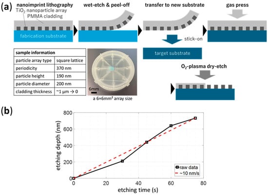
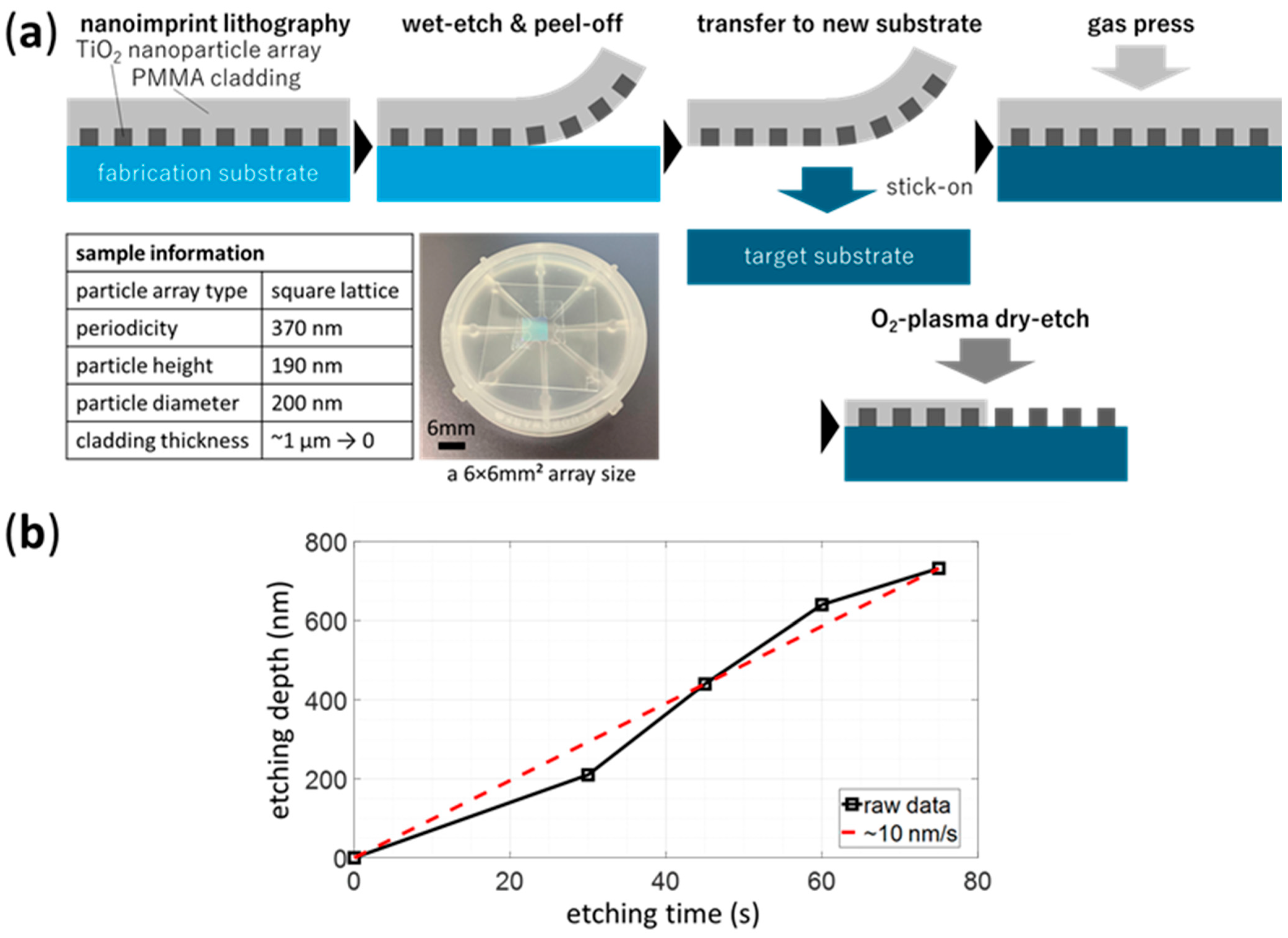
The fabrication and manipulation process is illustrated in Figure 1a, which is divided into three substeps described below. The characterizing methods, both experimental and numerical, are also shown.
Figure 1.
Illustration of the fabrication and manipulation (i.e., transfer and post-transfer process) of the metasurfaces used in this work. (a) Schematic of the experimental process flow and sample design information. (b) Etch-rate characterization of the dry oxygen-plasma RIE process, showing a nearly linear PMMA removal rate of about 10 nm/s in etch depth.
2.1. Fabrication of Metasurface
A metasurface consisting of a nanoparticle array of rutile-crystalline TiO2 was fabricated through thermal oxidation of a metallic Ti nanoparticle array [38]. A titanium thin film with a thickness of 150 nm was deposited onto the SiO2 substrate by electron beam evaporation (EB1200, CANON ANELVA, Kawasaki, Japan) under a vacuum pressure of 1.5 × 10⁻⁴ Pa, followed by spin-coating of a TU7-170 resist (Obducat, Lund, Sweden). Separately, a silicon master mold for nanoimprint was made through electron beam lithography (F7000S-KYT01, Advantest, Tokyo, Japan) and deep ICP etching (RIE-800iPB-KU, Samco, Kyoto, Japan). This master mold was employed to pattern the TU7-170 resist using nanoimprint lithography (Eitre3, Obducat, Sweden). Then, the titanium nanoparticle array was formed by reactive ion etching (uGmni-200E, Ulvac, Chigasaki, Japan) through the Ti film with a resist pattern as the mask. The titanium nanoparticle array was converted into a rutile-TiO2 nanoparticle array through oxidation by rapid thermal annealing at 750 °C in O2 atmosphere for 10 min. The rutile-TiO2 nanoparticle array thus obtained had a nanoparticle arrangement in a square lattice, a periodicity of 370 nm, a particle diameter of 200 nm, and a particle height of 190 nm. These geometrical parameters were set so that the resulting metasurface could support a desirable optical resonance [26,39,40].
2.2. Transfer Using PMMA Layer
Subsequently, the metasurface was transferred onto another SiO2 substrate. The metasurface was first coated with a ~1 μm thick PMMA through spin-coating with a solution of 10 wt% PMMA molecules (average molecular weight: 996,000) in anisole, followed by baking on a hot plate at 120 °C for 5 min. The whole sample was then immersed in a 5 wt% HF aqueous solution for selective wet-etching of the SiO2 substrate. As a result, the metasurface layer lifted off from the substrate and floated on the surface of the solution, thereby becoming ready for transfer. The transfer process was finalized by picking up the metasurface layer from the solution, placing it onto a new SiO2 substrate and draining and expelling the gap between the layer and the substrate using air gas pressure.
2.3. Post-Transfer Thinning and Removal of PMMA
After the transfer of the metasurface, the residual PMMA matrix was precisely thinned or completely removed by a dry-etching process. Specifically, the PMMA cladding was tailored via a selective RIE (RIE-10NR, Samco, Japan) with oxygen plasma. The etching process was carried out under 10 Pa chamber pressure with a 20 sccm oxygen gas flow and a 100 W RF discharge power, resulting in a steady etch rate of around 10 nm/s, as shown in Figure 1b. This opens a smooth path for post-fabrication adjustment and optimization of the optical properties of the metasurface as its resonance behavior is largely determined by the layer thickness [37,41,42]. As this solvent-free approach eliminates liquid-phase events such as flow or flushing, this gentle post-transfer process is particularly friendly to devices with a weak interlayer adhesion.
2.4. Optical Characterization
The optical characteristics of the metasurface layer were determined by examining the angle-dependent transmission spectrum [43]. This angle-resolved spectrum of the metasurface was measured using a home-built optical platform combining a transmission setup with a motorized rotational sample stage.
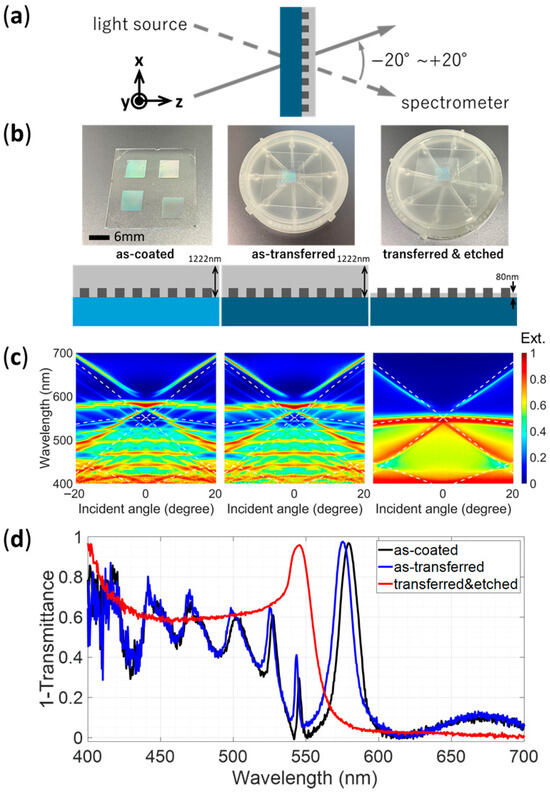
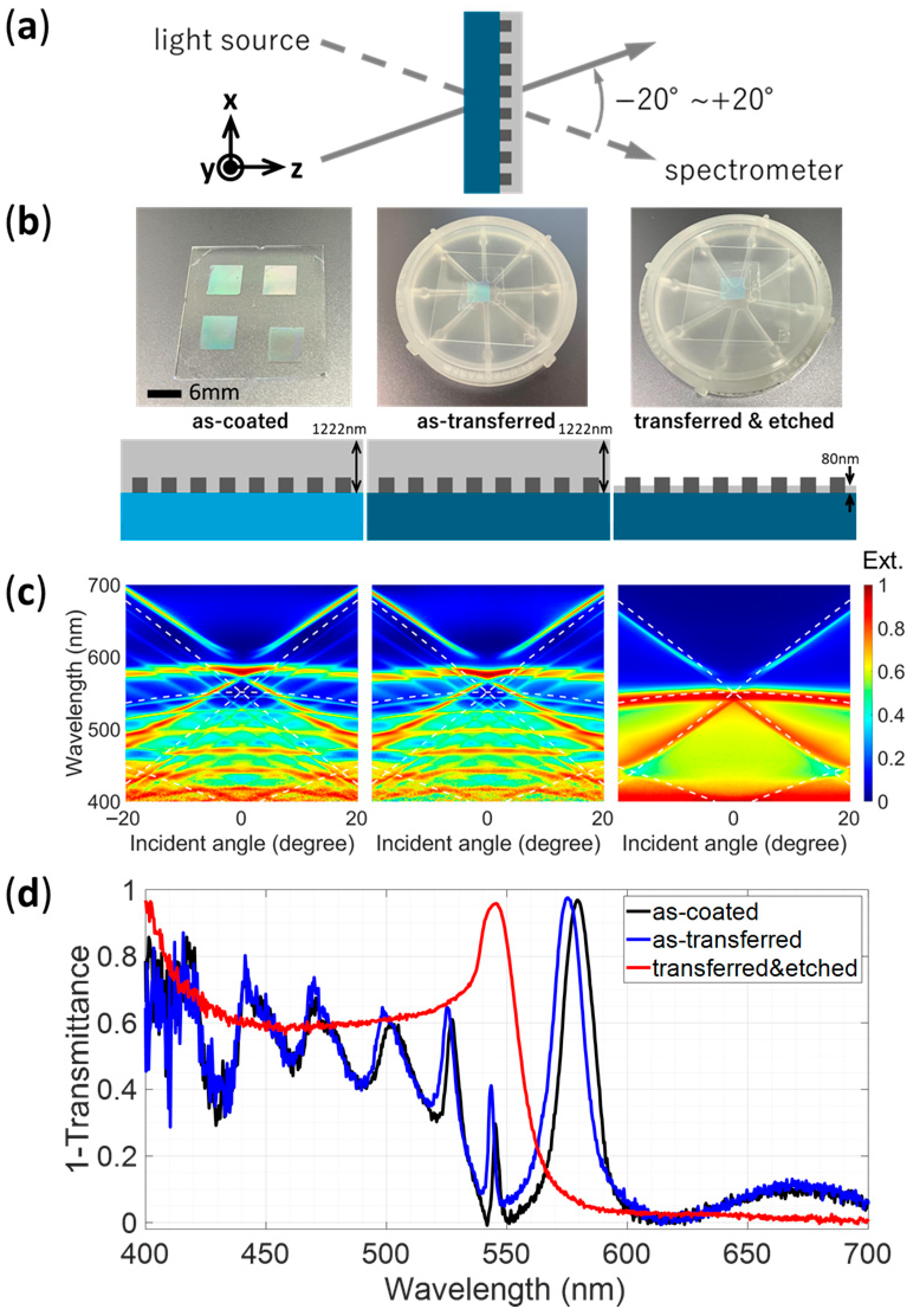
A halogen lamp was utilized as the broadband source. White light was emitted from the lamp and then coupled to the optical platform via a fiber, collimated by objective lenses, and passed through an iris hole for alignment and beam shaping. The incident beam was then linearly polarized to TE polarization using a plate polarizer. This collimated and polarized beam was directed onto the sample, which was mounted on a motorized rotation stage. The transmitted light was gathered into the tip of an optical fiber by a focal lens and detected by a spectrometer. An incidence angle ranging from −20° to +20° was scanned over in the zx plane, with the metasurface being placed on the xy plane as illustrated in Figure 2a.
Figure 2.
Optical resonance behavior characterization. (a) Schematic of the setup of the transmittance measurement. (b) Pictures of the transferable metasurface sample (from left to right), as-coated, transferred, and etched. (c) Angle-resolved extinction spectra of the sample at the corresponding stages, measured for TE-polarized illumination while scanning the incidence angle in the zx plane. The dotted lines refer to the in-plane diffraction conditions, i.e., Rayleigh anomalies. (d) Direct comparison between the extinction spectra at normal incidence for the three stages.
2.5. Simulation
To analyze the optical resonance of the metasurface layer, a numerical full-wave electromagnetic simulation based on the finite element method was carried out using commercial software COMSOL Multiphysics® (6.1). The model built for simulation consisted of a unit cell of square lattice arrangement containing a semi-ellipsoid nanoparticle, with refractive index n being 2.4 representing TiO2, at its center, on an SiO2 substrate (n = 1.46). A Floquet periodic boundary condition was set up for each pair of boundaries in the x and y dimensions with a unit cell size of 370 nm × 370 nm. In the z dimension, the whole cell was sandwiched by a pair of perfectly matched layers to assure effective infiniteness in the vertical directions. The diameter and height of the nanoparticle were set to be 200 nm and 190 nm, respectively. An extinction spectrum for TE-polarized light at normal incidence was computed for varied PMMA (n = 1.49) cladding thickness from 0 nm to 1222 nm.
3. Results
3.1. Optical Characterization
The optical pictures are compared between the samples, as-coated, after the transfer process, and after a 100 s etching of the PMMA cladding, in Figure 2b. The whole metasurface area (6 mm × 6 mm) is transferred with a PMMA cladding. The samples’ angle-dependent transmission spectra are plotted in Figure 2c. Extinction, defined as 1-transmittance, is exhibited instead of transmittance for a more straightforward data interpretation. The information-rich spectra reveal the photonic band structure [44], as a fingerprint of the optical resonance behavior of the metasurfaces. For the as-coated and as-transferred samples, the extinction maps consist of two linearly dispersive bands and one parabolic one, which are crossed at λ = 570 nm at normal incidence. Also shown in the map as dotted lines are the in-plane diffraction conditions or Rayleigh anomalies for a square lattice with period 370 nm and n = 1.49. The linear and parabolic features follow Rayleigh anomalies with a redshift. As revealed with the aid of simulation, the parabolic band is magnetic SLR where the magnetic dipoles (MDs) excited in each nanoparticle are coupled via diffraction, while the linear ones are electric SLRs between electric dipoles (EDs) and diffraction. Also, the fringe pattern at shorter wavelengths comes from Fresnel-type interference in the PMMA layer. The fringe pattern is sensitive to the film thickness, and the almost-identical patterns indicate the PMMA layer thickness is unchanged during the transfer process. On the other hand, when the PMMA cladding is etched for 100 s down to a lower thickness, the photonic resonance behavior of the sample is largely altered. The SLR features are preserved, though they are blueshifted, implying the nanoparticle patterns are retained [45] while thinning the PMMA reduces the effective refractive index surrounding PMMA. The fringe pattern vanishes completely due to the etching.
Figure 2d compares extinction spectra at normal incidence. The similarity between the spectra before and after transfer is further confirmed. It is noted that the spectra are not normalized, meaning that the extinction intensity is also retained. This means that the PMMA thickness, nanoparticle size and array arrangement are preserved during the transfer. The etched sample shows only one peak at λ = 546 nm, which is the magnetic SLR.
3.2. Simulation Study
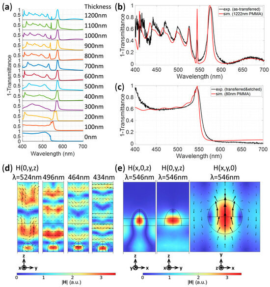
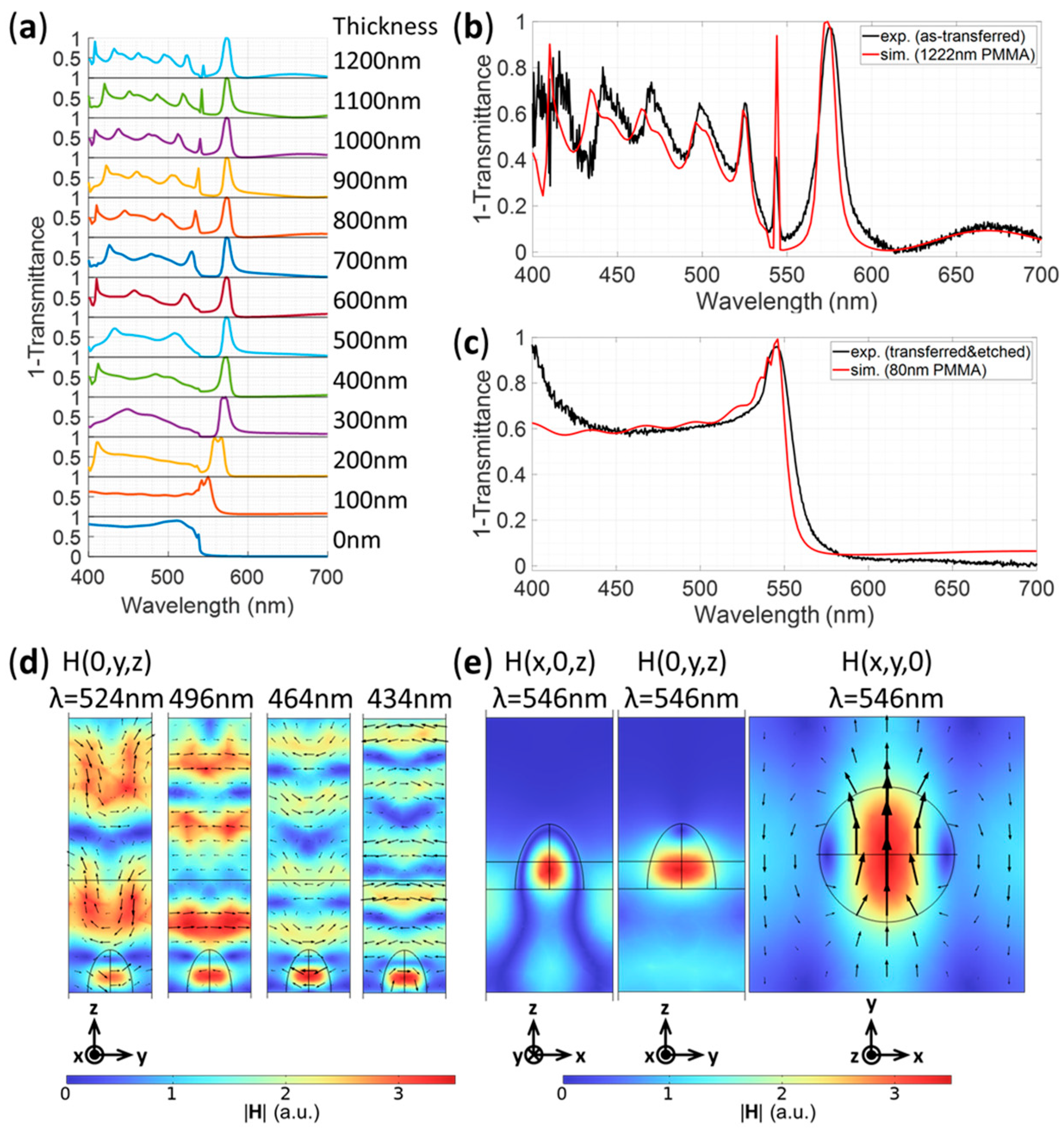
The simulated spectra at normal incidence with varying PMMA thickness are shown in Figure 3a. For the thickest layer of 1200 nm, a MD SLR peak appears at λ = 574 nm, and Fresnel-type fringes are observed at shorter wavelengths. As the thickness decreases, the MD SLR peak continuously blueshifts and the number of fringes decreases. The fringe disappears at a PMMA thickness of 100 nm, and finally the MD SLR disappears when PMMA is completely removed, and a small dip at λ = 536 nm appears which is the RA condition. For the as-coated sample and that etched for 100 s, the best fit to the experimental spectra was achieved for PMMA thicknesses of 1222 nm and 80 nm, respectively (Figure 3b,c).
Figure 3.
Simulated thickness-dependent optical response of the transferable rutile-TiO2 metasurface and comparison with experiment at representative cladding thicknesses. (a) Normal-incidence extinction spectra computed by full-wave finite element method simulation (COMSOL Multiphysics®) for metasurface layer with varied PMMA cladding thickness. (b,c) Normal-incidence extinction spectra simulated for (b) PMMA = 1222 nm and (c) 80 nm. Also shown are the experimental spectra for (b) as-transferred sample and (c) after etching for 100 s. (d) Magnetic field profiles of the multi-resonance modes observed in (b) the 1222 nm thick cladding sample. (e) Magnetic field profiles of the modes observed in (c) the 80 nm thick cladding sample. The arrows in (d,e) denote the flow of magnetic field.
Figure 3d,e show the spatial distribution of magnetic field at several characteristic wavelengths. The field distribution at λ = 524, 496, 464, and 434 nm exhibits a standing wave inside the layer with different number of nodes depending on the wavelength. The 80 nm (Figure 3d) case corresponds to the transferred and etched metasurface (right after the 100 s oxygen-plasma dry-etching) where the optical response is dominated by a single MD resonance with all higher-order modes switched off. The best fit by the simulation result after etching indicates a removal depth of 1142 nm. This is deeper than the value predicted from the etching rate in Figure 1b, where a 1000 nm PMMA layer was removed during the 100 s etching. Because this etching rate was obtained for the flat PMMA film on the unstructured substrate, the etch rate would be different for that on the nanoparticle arrays.
From the result of simulation, it is perceived that the optical response of the metasurface alters and shifts continuously along with the PMMA thickness. Moreover, the adjustability of metasurface optical behavior by layer thickness originates from the simultaneous multi-resonance modes [37] of the metasurface induced by the collective in-plane magnetic dipolar SLRs [46,47] and slab waveguiding supported by the high-refractive-index PMMA layer [48]. When the PMMA cladding is truncated down to an ultrathin, subwavelength thickness such as 80 nm, the multi-resonance modes are switched off, leaving alone the magnetic-dipole SLRs without any accompanying higher-order quasi-waveguide modes [48,49,50,51] coupled to the nanoparticle resonance [35].
3.3. Benchmarking
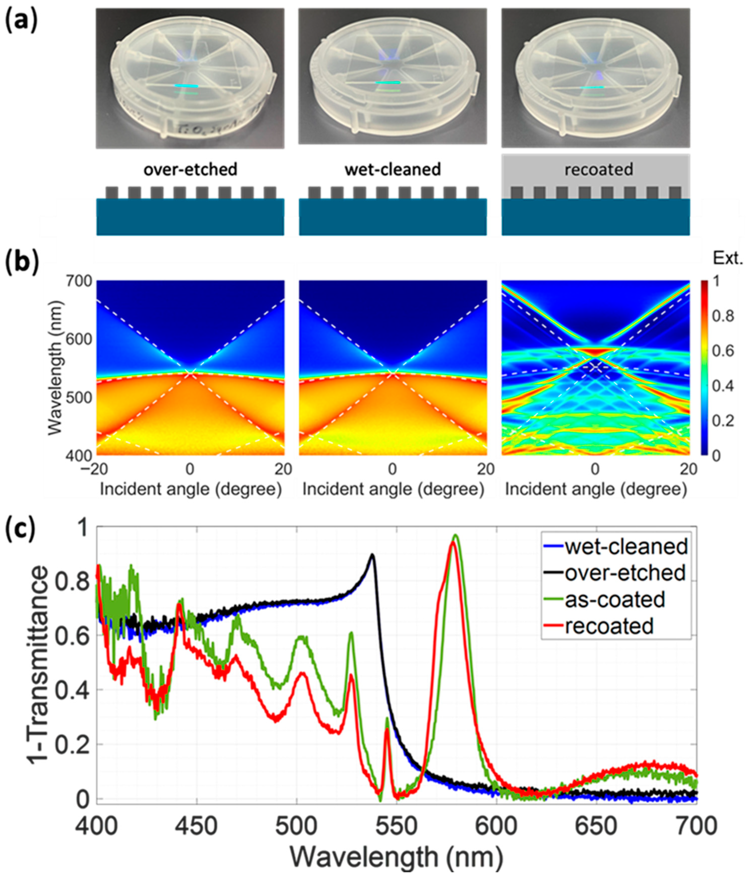
In most cases, a removal of PMMA cladding is necessary after the metasurface is transferred for subsequent manipulation and implementation of the optical resonator, such as integration of the nanostructure with liquids or gases as a sensor. The post-transfer treatment on PMMA by dry-etching is capable of not only precisely adjust its thickness, but also removing all residual PMMA efficiently and safely. In this subsection, the extinction spectrum of the metasurface with its PMMA cladding over-etched for 5 min is compared with a benchmark spectrum. The benchmark was obtained after the as-transfer sample underwent a 120 °C bake for 30 min followed by a 1 h ultrasonic bath in acetone, a typical wet-cleaning procedure commonly used in previous studies to completely remove PMMA [29,30]. Furthermore, it is also achievable to recoat a PMMA covering of arbitrary thickness. To prove this concept, a PMMA cladding with the same thickness as the initially fabricated and coated metasurface was recoated onto the transferred and over-etched metasurface.
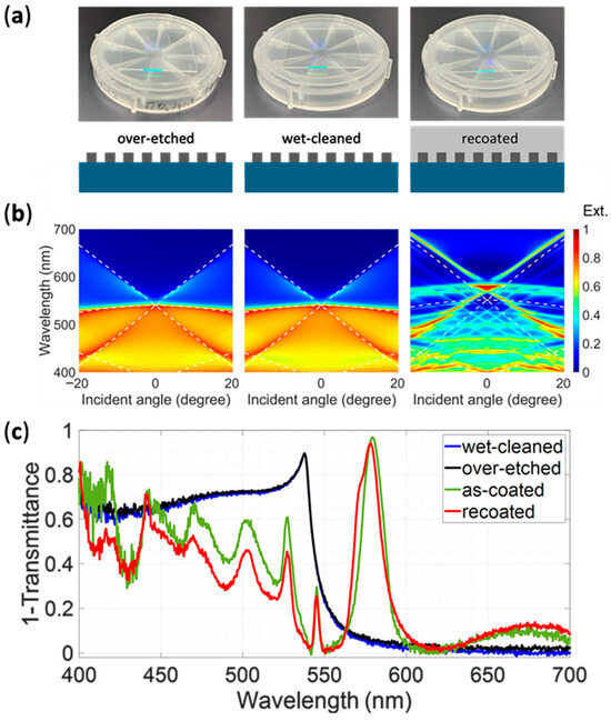
The optical picture and extinction maps are shown in Figure 4a,b, respectively. The good agreement between the results of the two approaches, dry-etch and wet-etch, validates the successful and complete removal of PMMA and the dry post-processing method proposed in this work as a competent alternative to the conventional wet-treatment method. The extinction for the recoated sample exhibits that the original photonic behavior is largely retrieved, confirming that the geometry of the nanoparticle resonators is protected throughout the whole process and that the metasurface layer supports and withstands repeatable and flexible manipulation.
Figure 4.
Benchmarking of post-transfer process method on the transferable metasurface. (a) Photos and schematics of the transferred metasurface sample (from left to right), after 5 min dry-etching (over-etched), 1 h wet-cleaning (wet-cleaned), and recoating with PMMA (recoated). (b) Angle-resolved extinction spectra of the sample at the corresponding stages. The dotted lines refer to the in-plane diffraction conditions, i.e., Rayleigh anomalies. (c) Normal-incidence extinction spectra of the sample at the corresponding stages.
Specifically, normal-incidence extinction spectra are shown in Figure 4c for the transferred metasurface after complete removal of the PMMA cladding using the two above-mentioned post-transfer treatments: oxygen-plasma dry-etching for 5 min and a conventional wet-cleaning treatment consisting of a 120 °C bake for 30 min followed by a 1 h ultrasonic bath in acetone. Again, the close agreement between the extinction spectra obtained by the two methods confirms the effective and complete removal of PMMA by the dry-etching approach. In addition, the extinction spectrum of the metasurface after recoating a PMMA cladding with the same thickness as the initially fabricated and coated layer (as-coated, prior to transfer) is presented, showing that the original optical response is largely retrieved. These results show not only the reliability of the oxygen-plasma dry-etching post-processing as a gentle and efficient alternative to conventional wet-cleaning, but also the robustness and repeatable tunability of the transferred metasurface under successive removal and reapplication of its polymer cladding.
4. Discussion
The results presented in this work demonstrate a versatile strategy for transferring and post-processing metasurfaces while conserving their nanostructure integrity and optical functionality. A key outcome of this study is the observation that the photonic band structure of the rutile-TiO2 nanoparticle metasurface remains essentially unchanged during the transfer process, as evidenced by the angle-resolved extinction spectroscopy. This indicates that the nanoscale geometry and layer thickness of the metasurface, which govern the resonance behavior, are not significantly distorted during the process. Compared with previously reported metasurface transfer methods, the present PMMA-supported transfer approach realizes a substantially larger transferable pattern size (of an area up to 6 mm × 6 mm) together with an in situ tunable, faster, and gentler post-transfer treatment (as compiled in Table 1) by exploiting nanoimprint lithography for metasurface fabrication and RIE for PMMA cladding thinning, thereby offering an improved mechanical stability, reproducibility, and scalability towards potential industrial application.
Table 1.
Comparison of representative PMMA-assisted metasurface transfer approaches.
The ability to precisely tailor the optical response of the transferred metasurface through exactly controlled thinning of the PMMA cladding constitutes another major advantage of the proposed method. Both experimental characterization and numerical simulation reveal that the resonance behavior of the metasurface evolves continuously as the PMMA thickness is reduced, with multi-resonance branches progressively blueshifting and disappearing. This behavior can be understood as the gradual suppression of slab-waveguide modes supported by the high-refractive-index PMMA layer and their coupling to the collective in-plane magnetic-dipole resonance of the nanoparticle resonators positioned in a square lattice. In the ultrathin-cladding regime, where the PMMA layer thickness becomes subwavelength, the optical response feature converges to a dominant MD resonance. This continuous and predictable thickness-dependent tuning provides a practical route for in situ optimization of metasurface performance after redeposition.
From a practical standpoint, replacing conventional wet-etching treatments with oxygen-plasma dry-etching for post-transfer PMMA matrix modification or removal significantly enhances material compatibility and process efficiency. Wet-cleaning approaches based on organic solvents such as acetone may introduce architectural or chemical incompatibility with functional layers, particularly in integrated or multilayer photonic devices. In contrast, the solvent-free dry-etching process demonstrated here allows gentle, rapid, and nanoscale-precise layer thickness control while minimizing the possibility of mechanical and chemical damage. The benchmarking result further shows that complete PMMA removal and subsequent recoating can be performed without degrading the metasurface, highlighting the reconfigurability and durability of the transferred layer.
Overall, this work displays transferable metasurfaces not merely as a passive structures that are relocated from one substrate to another, but as actively tunable optical components whose properties can be engineered in situ after integration. This capability is particularly relevant for applications involving curved structures, stacked photonic architectures, or functional overlays such as metalenses, sensing layers, or organic emitters. Future studies may extend this approach to other high-refractive-index dielectric materials and explore curved-plane and/or stacked-layer architectures by combining the transferable metasurface with multifarious optical structures and devices.
5. Conclusions
In summary, we have developed and demonstrated a flexible, efficient, and highly controllable fabrication and transfer technique for dielectric metasurfaces by embedding a rutile-TiO2 nanoparticle array into a PMMA matrix. The resulting transferable metasurface layer can be cleanly detached from its original substrate, transferred onto arbitrary target substrates, and subsequently modified through a solvent-free oxygen-plasma dry-etching process. Angle-resolved optical characterization confirms that the photonic band structure and resonance features of the metasurface are well preserved throughout the transfer process.
By precisely tuning the thickness of the PMMA cladding after transfer, the optical response of the metasurface can be continuously and predictably adjusted, ranging from multi-mode resonance behavior to a single magnetic-dipole resonance. Full-wave electromagnetic simulations corroborate experimental observations and elucidate the physical origins of the thickness-dependent resonance evolution. Compared with conventional wet-etching-based post-transfer treatments, the proposed dry-etching approach offers superior precision, speed, and compatibility with solvent-sensitive materials and weakly bonded multilayer systems.
The presented method expands the toolbox for metasurface manipulation, integration, and post-fabrication in situ optimization, enabling the deployment of high-performance nanophotonic components in complex and unconventional device architectures. This approach paves the way toward scalable, reconfigurable, and application-oriented metasurface technologies for sensing, integrated photonics, and advanced optical systems.
Author Contributions
Conceptualization, Y.S. and S.M.; methodology, Y.S.; software, Y.S.; validation, Y.S., T.L. and T.T.; formal analysis, Y.S.; investigation, Y.S.; resources, Y.S.; data curation, Y.S.; writing—original draft preparation, Y.S.; writing—review and editing, S.M. and K.T.; visualization, Y.S.; supervision, S.M. and K.T.; project administration, Y.S.; funding acquisition, S.M. and K.T. All authors have read and agreed to the published version of the manuscript.
Funding
This work was partly supported by the Nanotechnology Hub, Kyoto University. We gratefully acknowledge financial support from Kakenhi (25K01501, 25K21709), and Bilateral (Japan–China (NSFC)) Joint Research Project (120247409). TYL acknowledges Grant-in-Aid for JSPS Fellowship (24KJ1423).
Institutional Review Board Statement
Not applicable.
Informed Consent Statement
Not applicable.
Data Availability Statement
The raw data supporting the conclusions of this article will be made available by the authors on request.
Acknowledgments
During the preparation of this manuscript, the authors used ChatGPT 5.3 for the purposes of superficial text editing (grammar correction and text revision). The authors have reviewed and edited the output and take full responsibility for the content of this publication.
Conflicts of Interest
The authors declare no conflicts of interest.
Abbreviations
The following abbreviations are used in this manuscript:
| HF | Hydrogen Fluoride |
| PDMS | Poly(dimethylsiloxane) |
| PMMA | Poly(methyl methacrylate) |
| PVC | Poly(vinyl chloride) |
| RF | Radio Frequency |
| RIE | Reactive Ion Etching |
| TE | Transverse Electric |
References
- Neshev, D.; Aharonovich, I. Optical Metasurfaces: New Generation Building Blocks for Multi-Functional Optics. Light Sci. Appl. 2018, 7, 58. [Google Scholar] [CrossRef] [Scilit] [PubMed]
- Jiang, Q.; Hu, L.; Geng, G.; Li, J.; Wang, Y.; Huang, L. Arbitrary Amplitude and Phase Control in Visible by Dielectric Metasurface. Opt. Express 2022, 30, 13530–13539. [Google Scholar] [CrossRef] [Scilit]
- Yu, J.; Kim, J.; Chung, H.; Son, J.; Boehm, G.; Belkin, M.A.; Lee, J. Full Complex Amplitude Control of Second-Harmonic Generation via Electrically Tunable Intersubband Polaritonic Metasurfaces. Sci. Adv. 2025, 11, eadw8852. [Google Scholar] [CrossRef] [Scilit] [PubMed]
- Dorrah, A.H.; Park, J.-S.; Palmieri, A.; Capasso, F. Free-Standing Bilayer Metasurfaces in the Visible. Nat. Commun. 2025, 16, 3126. [Google Scholar] [CrossRef] [Scilit]
- Ni, X.; Emani, N.K.; Kildishev, A.V.; Boltasseva, A.; Shalaev, V.M. Broadband Light Bending with Plasmonic Nanoantennas. Science 2012, 335, 427. [Google Scholar] [CrossRef] [Scilit] [PubMed]
- Babicheva, V.E.; Chang, C.-C. Atomic Layer Deposition for Enhanced Light Confinement in Nonlinear Metasurfaces. ACS Omega 2025, 10, 23150–23160. [Google Scholar] [CrossRef] [Scilit]
- Lin, Y.-T.; Hassanfiroozi, A.; Jiang, W.-R.; Liao, M.-Y.; Lee, W.-J.; Wu, P.C. Photoluminescence Enhancement with All-Dielectric Coherent Metasurfaces. Nanophotonics 2022, 11, 2701–2709. [Google Scholar] [CrossRef] [Scilit]
- Lin, C.-H.; Huang, S.-H.; Lin, T.-H.; Wu, P.C. Metasurface-Empowered Snapshot Hyperspectral Imaging with Convex/Deep (CODE) Small-Data Learning Theory. Nat. Commun. 2023, 14, 6979. [Google Scholar] [CrossRef] [Scilit]
- Kim, H.; Yun, H.; Jeong, S.; Lee, S.; Cho, E.; Rho, J. Optical Metasurfaces for Biomedical Imaging and Sensing. ACS Nano 2025, 19, 3085–3114. [Google Scholar] [CrossRef] [Scilit]
- Choi, D.; Zachariah, S.; Kaurav, R.; Fang, J.; Chen, J.; Laursen, B.W.; Flood, A.H.; Majumdar, A.; Alù, A.; Menon, V.M. Highly Coherent Organic Lasing Based on Etch-Free Metasurface. Nat. Commun. 2025, 17, 906. [Google Scholar] [CrossRef] [Scilit]
- Cheng, J.; Jafar-Zanjani, S.; Mosallaei, H. All-Dielectric Ultrathin Conformal Metasurfaces: Lensing and Cloaking Applications at 532 Nm Wavelength. Sci. Rep. 2016, 6, 38440. [Google Scholar] [CrossRef] [Scilit]
- Kim, J.; Jeon, W. Nonplanar Metasurface for Perfect Absorption of Sound Waves. J. Acoust. Soc. Am. 2021, 149, 2323–2336. [Google Scholar] [CrossRef] [Scilit]
- Gong, J.; Xiong, L.; Pu, M.; Wen, Y.; Cai, J.; Feng, X.; Pan, R.; He, Q.; Guo, Y.; Chi, N.; et al. High-Throughput Fabrication of Curved Plasmonic Metasurfaces for Switchable Beam Focusing and Thermal Infrared Cloaking. Adv. Opt. Mater. 2023, 11, 2300608. [Google Scholar] [CrossRef] [Scilit]
- Yang, S.; Ma, H.; Zhang, Y.; Yin, M.; Ma, H.; Chen, T.; Zhang, T.; Deng, L.; Chen, Q. Tunable Stealth Curved Metasurface Based on Laser Reversible Induction Technology. Opt. Express 2025, 33, 44454–44473. [Google Scholar] [CrossRef] [Scilit]
- Shiri, Y.; Guerboukha, H.; Mittleman, D.M. Terahertz Beam Steering with Curved Metasurfaces. J. Infrared Millim. Terahertz Waves 2023, 44, 397–406. [Google Scholar] [CrossRef] [Scilit]
- Zhou, Y.; Kravchenko, I.I.; Wang, H.; Nolen, J.R.; Gu, G.; Valentine, J. Multilayer Noninteracting Dielectric Metasurfaces for Multiwavelength Metaoptics. Nano Lett. 2018, 18, 7529–7537. [Google Scholar] [CrossRef] [Scilit]
- Gromyko, D.; An, S.; Gorelik, S.; Xu, J.; Lim, L.J.; Lee, H.Y.L.; Tjiptoharsono, F.; Tan, Z.-K.; Qiu, C.-W.; Dong, Z.; et al. Unidirectional Chiral Emission via Twisted Bi-Layer Metasurfaces. Nat. Commun. 2024, 15, 9804. [Google Scholar] [CrossRef] [Scilit] [PubMed]
- Aftenieva, O.; Schnepf, M.; Mehlhorn, B.; König, T.A.F. Tunable Circular Dichroism by Photoluminescent Moiré Gratings. Adv. Opt. Mater. 2021, 9, 2001280. [Google Scholar] [CrossRef] [Scilit]
- Jordaan, J.; Minovich, A.E.; Neshev, D.; Staude, I. Design of Multilayer Huygens’ Metasurfaces for Large-Area Multiwavelength and Polarization- Insensitive Metalenses. Opt. Express 2025, 33, 33643–33654. [Google Scholar] [CrossRef] [Scilit] [PubMed]
- Choi, S.; Zuo, J.; Das, N.; Yao, Y.; Wang, C. Scalable Nanoimprint Manufacturing of Functional Multilayer Metasurface Devices. Adv. Funct. Mater. 2024, 34, 2404852. [Google Scholar] [CrossRef] [Scilit]
- Ko, J.; Kim, G.; Kim, I.; Hwang, S.H.; Jeon, S.; Ahn, J.; Jeong, Y.; Ha, J.-H.; Heo, H.; Jeong, J.-H.; et al. Metasurface-Embedded Contact Lenses for Holographic Light Projection. Adv. Sci. 2024, 11, 2407045. [Google Scholar] [CrossRef] [Scilit] [PubMed]
- Biabanifard, M.; Xiao, J.; Di Falco, A. Thin-Film Polymeric Metasurfaces for Visible Wavelengths. Appl. Phys. Lett. 2023, 123, 231702. [Google Scholar] [CrossRef] [Scilit]
- Gan, Y.; Xiao, J.; Plaskocinski, T.; Persheyev, S.; Biabanifard, M.; Di Falco, A. See-Through Conformable Holographic Metasurface Patches for Augmented Reality. Laser Photonics Rev. 2025, 19, 2401240. [Google Scholar] [CrossRef] [Scilit]
- Choi, H.; Kim, J.; Kim, W.; Seong, J.; Park, C.; Choi, M.; Kim, N.; Ha, J.; Qiu, C.-W.; Rho, J.; et al. Realization of High Aspect Ratio Metalenses by Facile Nanoimprint Lithography Using Water-Soluble Stamps. PhotoniX 2023, 4, 18. [Google Scholar] [CrossRef] [Scilit]
- Onodera, M.; Wakafuji, Y.; Hashimoto, T.; Masubuchi, S.; Moriya, R.; Zhang, Y.; Watanabe, K.; Taniguchi, T.; Machida, T. All-Dry Flip-over Stacking of van Der Waals Junctions of 2D Materials Using Polyvinyl Chloride. Sci. Rep. 2022, 12, 21963. [Google Scholar] [CrossRef] [Scilit]
- Agata, K.; Murai, S.; Tanaka, K. Stick-and-Play Metasurfaces for Directional Light Outcoupling. Appl. Phys. Lett. 2021, 118, 021110. [Google Scholar] [CrossRef] [Scilit]
- Park, Y.; Kim, J.; Yang, Y.; Oh, D.K.; Kang, H.; Kim, H.; Rho, J. Tape-Assisted Residual Layer-Free One-Step Nanoimprinting of High-Index Hybrid Polymer for Optical Loss-Suppressed Metasurfaces. Adv. Sci. 2025, 12, 2409371. [Google Scholar] [CrossRef] [Scilit] [PubMed]
- Shi, Y.; Dai, H.; Tang, R.; Wu, J.; Wu, Y.; Song, J.; Si, Y.; Lin, H.; Li, L. Flexible Multilayer Metasurfaces: Design and Applications on Foldable and Conformable Substrates. Adv. Mater. Technol. 2025, 10, 2402130. [Google Scholar] [CrossRef] [Scilit]
- Zhang, X.; Cai, H.; Rezaei, S.D.; Rosenmann, D.; Lopez, D. A Universal Metasurface Transfer Technique for Heterogeneous Integration. Nanophotonics 2023, 12, 1633–1642. [Google Scholar] [CrossRef] [Scilit] [PubMed]
- Zhang, Y.; Zhang, Z.; Xu, C.; Lu, W.; Chen, Z.; Wang, C.; Xiao, F.; Wang, S.; Li, X. Precisely Constructing Hybrid Nanogap Arrays via Wet-Transfer of Dielectric Metasurfaces onto a Plasmonic Mirror. Opt. Express 2023, 31, 34280–34291. [Google Scholar] [CrossRef] [Scilit]
- Kim, M.; Park, N.-R.; Yu, A.; Kim, J.T.; Jeon, M.; Jeon, S.-W.; Han, S.-W.; Kim, M.-K. Multilayer All-Polymer Metasurface Stacked on Optical Fiber via Sequential Micro-Punching Process. Nanophotonics 2023, 12, 2359–2369. [Google Scholar] [CrossRef] [Scilit]
- He, F.; Fuentes-Domínguez, R.; Cousins, R.; Mellor, C.J.; Rocha, A.D.; Adams, Z.; Barton, J.K.; Gordon, G.S.D. Scalable Fabrication of Single- and Multi-Layer Planar Lenses on Fiber Imaging Probes. APL. Photonics 2025, 10, 056114. [Google Scholar] [CrossRef] [Scilit]
- Roggero, U.F.S.; Rojas-Bejarano, C.J.; Herreño-Fierro, C.A.; Seifert, A.; Garcia-Etxarri, A.; Hernández-Figueroa, H.E.; Zapata-Herrera, M. Surface Lattice Resonances for High-Performance Sensing: A Study on Gold Nanoparticle Arrays. Opt. Express 2025, 33, 30328–30341. [Google Scholar] [CrossRef] [Scilit]
- Cherqui, C.; Bourgeois, M.R.; Wang, D.; Schatz, G.C. Plasmonic Surface Lattice Resonances: Theory and Computation. Acc. Chem. Res. 2019, 52, 2548–2558. [Google Scholar] [CrossRef] [Scilit]
- Kravets, V.G.; Kabashin, A.V.; Barnes, W.L.; Grigorenko, A.N. Plasmonic Surface Lattice Resonances: A Review of Properties and Applications. Chem. Rev. 2018, 118, 5912–5951. [Google Scholar] [CrossRef] [Scilit]
- Park, J.H.; Lee, S.H.; Choi, K.H.; Noh, H.S.; Lee, J.W.; Pearton, S.J. Comparison of Dry Etching of PMMA and Polycarbonate in Diffusion Pump-Based O2 Capacitively Coupled Plasma and Inductively Coupled Plasma. Thin Solid Films 2010, 518, 6465–6468. [Google Scholar] [CrossRef] [Scilit]
- Reshef, O.; Saad-Bin-Alam, M.; Huttunen, M.J.; Carlow, G.; Sullivan, B.T.; Ménard, J.-M.; Dolgaleva, K.; Boyd, R.W. Multiresonant High-Q Plasmonic Metasurfaces. Nano Lett. 2019, 19, 6429–6434. [Google Scholar] [CrossRef] [Scilit]
- Takashima, T.; Lo, T.Y.; Takane, H.; Murai, S.; Tanaka, K. Amorphous-Germania as an Annealing-Resistive and Water-Soluble Sacrifice Layer for Fabricating Metasurface Stickers. Jpn. J. Appl. Phys. 2025, 64, 03SP66. [Google Scholar] [CrossRef] [Scilit]
- Lo, T.Y.; Murai, S.; Tse, J.T.Y.; Tanaka, K. Nonlocal Coupling in Hybrid Bilayer Metasurfaces via Out-of-Plane Quadrupole Surface Lattice Resonance. Adv. Opt. Mater. 2025, 13, e02518. [Google Scholar] [CrossRef] [Scilit]
- Lo, T.; Murai, S.; Tanaka, K. Silver Nanoantenna Stickers for Photoluminescence Control. ACS Appl. Opt. Mater. 2023, 1, 870–877. [Google Scholar] [CrossRef] [Scilit]
- Chen, Y.; Zhang, Y.; Koenderink, A.F. General Point Dipole Theory for Periodic Metasurfaces: Magnetoelectric Scattering Lattices Coupled to Planar Photonic Structures. Opt. Express 2017, 25, 21358–21378. [Google Scholar] [CrossRef] [Scilit] [PubMed]
- Schokker, A.H.; van Riggelen, F.; Hadad, Y.; Alù, A.; Koenderink, A.F. Systematic Study of the Hybrid Plasmonic-Photonic Band Structure Underlying Lasing Action of Diffractive Plasmon Particle Lattices. Phys. Rev. B 2017, 95, 085409. [Google Scholar] [CrossRef] [Scilit]
- Guo, R.; Hakala, T.K.; Törmä, P. Geometry Dependence of Surface Lattice Resonances in Plasmonic Nanoparticle Arrays. Phys. Rev. B 2017, 95, 155423. [Google Scholar] [CrossRef] [Scilit]
- Eyvazi, S.; Mamonov, E.A.; Heilmann, R.; Cuerda, J.; Törmä, P. Flat-Band Lasing in Silicon Waveguide-Integrated Metasurfaces. ACS Photonics 2025, 12, 1570–1578. [Google Scholar] [CrossRef] [Scilit]
- Tse, J.T.Y.; Ong, H.C. Quality Factor of Plasmonic Monopartite and Bipartite Surface Lattice Resonances. Phys. Rev. B 2021, 104, 125442. [Google Scholar] [CrossRef] [Scilit]
- Huttunen, M.J.; Dolgaleva, K.; Törmä, P.; Boyd, R.W. Ultra-Strong Polarization Dependence of Surface Lattice Resonances with out-of-Plane Plasmon Oscillations. Opt. Express 2016, 24, 28279–28289. [Google Scholar] [CrossRef] [Scilit] [PubMed]
- Auguié, B.; Barnes, W.L. Collective Resonances in Gold Nanoparticle Arrays. Phys. Rev. Lett. 2008, 101, 143902. [Google Scholar] [CrossRef] [Scilit] [PubMed]
- Ramezani, M.; Lozano, G.; Verschuuren, M.A.; Gómez-Rivas, J. Modified Emission of Extended Light Emitting Layers by Selective Coupling to Collective Lattice Resonances. Phys. Rev. B 2016, 94, 125406. [Google Scholar] [CrossRef] [Scilit]
- Rodriguez, S.R.K.; Murai, S.; Verschuuren, M.A.; Rivas, J.G. Light-Emitting Waveguide-Plasmon Polaritons. Phys. Rev. Lett. 2012, 109, 166803. [Google Scholar] [CrossRef] [Scilit] [PubMed]
- Murai, S.; Verschuuren, M.A.; Lozano, G.; Pirruccio, G.; Rodriguez, S.R.K.; Rivas, J.G. Hybrid Plasmonic-Photonic Modes in Diffractive Arrays of Nanoparticles Coupled to Light-Emitting Optical Waveguides. Opt. Express 2013, 21, 4250–4262. [Google Scholar] [CrossRef] [Scilit]
- Christ, A.; Tikhodeev, S.G.; Gippius, N.A.; Kuhl, J.; Giessen, H. Waveguide-Plasmon Polaritons: Strong Coupling of Photonic and Electronic Resonances in a Metallic Photonic Crystal Slab. Phys. Rev. Lett. 2003, 91, 183901. [Google Scholar] [CrossRef] [Scilit] [PubMed]

Disclaimer/Publisher’s Note: The statements, opinions and data contained in all publications are solely those of the individual author(s) and contributor(s) and not of MDPI and/or the editor(s). MDPI and/or the editor(s) disclaim responsibility for any injury to people or property resulting from any ideas, methods, instructions or products referred to in the content. |
© 2026 by the authors. Licensee MDPI, Basel, Switzerland. This article is an open access article distributed under the terms and conditions of the Creative Commons Attribution (CC BY) license.