


Abstract
Topological edge and corner states show great promise for manipulating electromagnetic waves, but their limited mode area restricts practical applications. Here, we propose a topological terahertz photonic crystal with a three-layer heterostructure, in which the middle Dirac photonic crystal layer that exhibits Dirac-like dispersion supports large-area terahertz waveguide states. Quantitative analysis shows that valley-momentum-locked states maintain high transmission even at sharp bends and in the presence of defects. Additionally, we demonstrate topological large-area corner modes. The mode area scales with the number of photonic crystal layers that exhibit Dirac-like dispersion, as confirmed by numerical calculations. This work advances the flexible control of terahertz waves and holds significant potential for practical applications in topological photonics.
1. Introduction
In recent years, the concept of topology in electronic systems has been successfully extended to electromagnetic fields. Since then, remarkable progress has been achieved in topological photonic crystals (PCs). Among these, topological edge states have attracted considerable attention for their robust transmission, which is immune to sharp bends and structural defects [1,2,3]. Early realizations of topological PCs relied on magneto-optical systems under external magnetic fields, but these implementations were limited to the microwave regime [4,5]. Later, photonic topological insulators mimicking the quantum spin Hall effect were realized using bianisotropic metamaterials [6], but their fabrication was challenging. Subsequent breakthroughs were achieved in all-dielectric photonic crystals, in which topological phase transitions were induced through symmetry breaking [7,8,9]. Similarly, valley photonic crystals analogous to the quantum valley Hall effect were proposed via inversion symmetry breaking [10,11,12,13]. Recently, various functional devices, including topological waveguides [14,15], topological lasers [16,17,18], and other related photonic devices [19,20,21,22,23,24], have been demonstrated by utilizing valley topological edge states. According to the bulk-edge correspondence principle, topological edge states, such as chiral, helical, and valley edge states, emerge at the interfaces between photonic crystals with distinct Chern numbers [4,5,6,7,10]. These states support unidirectional propagation and exhibit strong robustness against disorders, defects, and sharp bends. In addition to its structural simplicity, broad operational bandwidth, and excellent fabrication tolerance, the valley photonic crystal platform offers key physical advantages, as it inherently links the valley degree of freedom with orbital angular momentum, enabling backscattering-immune edge states that open new avenues for chiral light manipulation and information encoding [11,12,13,14]. Recently, on-chip terahertz photonic interconnects constructed from amorphous topological structures have been shown to achieve efficient and robust terahertz wave transmission via topological protection [25].
Furthermore, high-order topological insulators have garnered widespread attention, owing to their ability to support exotic low-dimensional topological states that emerge in two-dimensional and higher-dimensional systems [26]. Higher-order topological insulators can be realized using two-dimensional photonic crystals with diverse lattice configurations, including honeycomb, square, and Kagome lattices [27,28,29,30,31], where corner states are confined at the structural corner with topological protection characteristics. Several research groups have successfully observed localized topological corner states for the first time across microwave, terahertz, and optical frequency regimes [32,33,34,35,36], using platforms such as microwave circuits and photonic crystal slabs. These experiments have confirmed signature properties of higher-order topological states, including their robustness against defects and disorder. Higher-order topological photonic crystals offer a new paradigm for manipulating light in lower dimensions, providing novel principles and pathways for realizing highly localized, disturbance-resistant on-chip photonic devices, such as lasers, resonators, and filters. They represent one of the most promising candidate technologies for advancing the development of future integrated photonic chips. However, conventional topological edge states suffer from limited energy flux and fixed waveguide widths, which restrict flexible control over energy channels and integration with conventional photonic systems. To address these challenges, researchers initially explored sonic crystal heterostructures, in which a photonic crystal layer exhibiting Dirac-like dispersion was embedded between two topologically distinct domains. These structures have been shown to support extended waveguide modes with topological protection [37,38,39]. Since then, this heterostructure concept has since been extended to photonic platforms through three complementary approaches. Magnetic photonic crystal heterostructures leverage time-reversal symmetry breaking to achieve one-way large-area transport with strong immunity to backscattering [40]. However, the incorporation of magnetic materials introduces integration complexities and additional losses, particularly at near-infrared wavelengths. All-dielectric valley photonic crystals offer an alternative that circumvents these issues by relying solely on inversion symmetry breaking [41,42]. In parallel, spin photonic crystals enable large-area topological waveguide states via a three-layer heterostructure design, overcoming the energy flux limitations inherent to conventional edge states. By sandwiching a photonic crystal layer with Dirac-like dispersion between expanded and shrunken photonic crystals exhibiting C6 symmetry, pseudospin-momentum-locked modes are generated. These modes exhibit uniform field distribution across the middle layer, supporting high energy flux and flexible control over mode area while maintaining robustness against bends and defects. Similarly, valley-locked waveguide modes also demonstrate broadband topological protection with significantly enhanced energy transmission. In contrast to conventional edge states, these heterostructure-guided modes can be engineered to sustain uniform intensity over large modal volumes, effectively addressing the power handling constraints of traditional designs. Furthermore, the valley degree of freedom enables selective excitation and directional routing, positioning this platform for advanced on-chip photonic information processing applications. For conventional higher-order topological states, extreme spatial localization simultaneously constrains their mode volume and energy distribution range, leading to fundamental challenges in application scenarios that require large-scale optical field manipulation, distributed energy harvesting and radiation, or long-range topological transport. Therefore, investigating large-area higher-order topological states is of pivotal importance. As it opens up new avenues toward scalable and functional topological devices.
We propose a three-layer heterostructure that integrates Dirac photonic crystals between two topologically distinct photonic crystals. This design supports large-area topological waveguide states, which are predominantly confined to the central layer exhibiting Dirac-like dispersion. These waveguide states exhibit valley-momentum locking and robust one-way propagation, even in the presence of defects and sharp bends. The design further achieves topological large-area corner states at heterojunction interfaces, which exhibit a larger mode area and higher energy capacity compared with conventional corner states. These extended topological states address key challenges in the terahertz range, including propagation loss, integration density, energy capacity, and field enhancement, paving the way for next-generation high-speed communication, ultrasensitive sensing, and quantum light sources.
2. Analysis of Sandwich-Structured Heterostructures and Their Band Properties
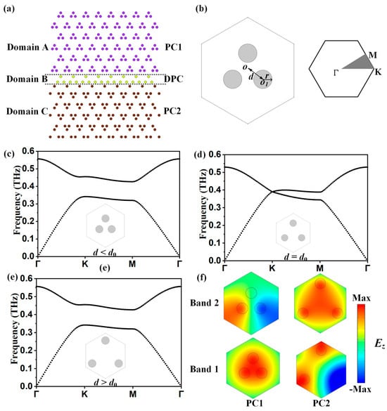
As illustrated in Figure 1a, the proposed three-layer heterostructure consists of three different regions: domain A, domain B, and domain C. These regions are realized using photonic crystals labeled PC1, DPC, and PC2, respectively, all of which share a consistent lattice constant of a = 300 μm. The unit cell configuration for each crystal is depicted in Figure 1b, where three cylindrical dielectric scatterers with r = 0.1a. And the relative dielectric constant is 11.7. The distance from the center of the rods to the center of the unit cell is d, which is different for PC1, DPC, and PC2. The parameter d is , , and , respectively. The first Brillouin zone corresponding to the Kagome lattice is plotted in Figure 1b. The band structures of the photonic crystals are computed by solving eigen equations using the finite-element analysis software COMSOL Multiphysics 5.5. Our work only focuses on the transverse magnetic (TM) mode, characterized by an out-of-plane electric field component (Ez) along with in-plane magnetic field components (Hx and Hy), while all other field components remain zero. Based on Maxwell’s equations, the corresponding eigenvalue equation can be expressed as:
where ε(r) is the position-dependent permittivity, E(r) is the position-dependent electric field vector, c denotes the speed of light in vacuum, and ω represents the angular frequency. The corresponding band structures for PC1, DPC, and PC2 are displayed in Figure 1c–e, respectively. For DPC, the distance between the intracell rods is the same as the distance between the intercell rods. This configuration results in equal coupling strengths for both intracell and intercell interactions among neighboring rods, consequently inducing degenerate Dirac cones at the K point in the Brillouin zone. As shown in Figure 1d, a two-fold degenerate Dirac cone appears at the frequency of 0.391 THz. Lifting the degeneracy at the Dirac point can introduce a complete bandgap, and the topological character of this gap is determined by the relative strength between the intracell and intercell coupling. For PC1, d < d0 indicates the intracell coupling is stronger than the intercell coupling, resulting in a topologically trivial phase. Its band structure is shown in Figure 1c, the two-fold degenerate Dirac cone is lifted, giving rise to a complete photonic bandgap from 0.3414 to 0.4264 THz. The electric field distributions of the eigenmodes at the K point (Figure 1f) reveal that the monopole-like mode exhibits a lower frequency than the dipole-like mode. In contrast, for PC2, d > d0 indicates the intracell coupling is weaker than the intercell coupling, so PC2 is topologically non-trivial. Although PC2 and PC1 share an identical band structure (Figure 1e), their mode ordering at the K point is reversed. For PC2, the monopole-like mode resonates at a higher frequency than the dipole-like mode. These distinctive characteristics confirm that PC1 and PC2 belong to different topological phases. In topological photonic crystals with a Kagome-lattice, the two-dimensional bulk polarization serves as the topological invariant that rigorously characterizes the underlying topological phases. The 2D bulk polarization can be expressed as:
Figure 1.
(a) Schematic diagram of the designed heterostructure, consisting of domains A, B, and C. (b) Schematic of the unit cell and the first Brillouin zone corresponding to the Kagome lattice. (c) Calculated band structures of PC1 with d < d0. (d,e) Dispersion relations for DPC with d = d0 and PC2 with d > d0, respectively. (f) Electric field intensity distributions of the eigenstates at the K point for both PC1 and PC2.
Here, denotes the Berry connection along the ki direction with i = x, y, and S represents the area of the Brillouin zone. The topological phase transition is thus captured by the bulk polarization P [34,35], which reflects the shift in the Wannier center from the lattice center to its corner as d/d0 varies. For the expanded case (d/d0 > 1), the bulk polarization is calculated to be P(1/3, 1/3), indicating a nontrivial topology for the expanded PCs. In contrast, for the shrunken case (d/d0 < 1), the bulk polarization is calculated to be P(0, 0), confirming the topologically trivial nature of the shrunken PCs [36].
3. Topological Large-Area Waveguide States
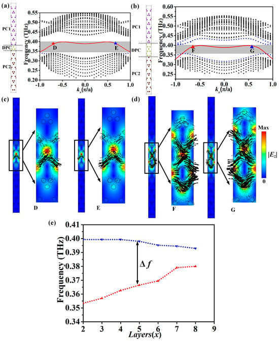
According to the bulk-edge correspondence principle, topologically protected edge modes typically emerge at the boundary between two domains possessing different topological invariants. In this work, however, we shift our focus to topological large-area waveguide states. To explore these, we construct an ABxC-type supercell where domain B has one layer with x = 1, as depicted in Figure 2a. Band structure calculations for this supercell confirm the existence of topological waveguide modes (highlighted by the red line). Furthermore, Figure 2c displays the electric field and Poynting vector distributions for eigenstates at a frequency of 0.39275 THz, corresponding to kx = −0.65π/a and kx = 0.65π/a (marked by red and blue five-pointed stars, labeled D and E, respectively). Notably, the electric energy is primarily confined within domain B, which distinguishes these states from conventional topological edge states. Specifically, the eigenstate D at kx = −0.65π/a exhibits forward energy propagation, whereas the eigenstate E at kx = 0.65π/a shows backward energy propagation. These states also display valley-locked characteristics and can be classified as topological large-area waveguide states. In addition, there are high-order non-topological waveguide states denoted by blue dotted lines, which are gapped and lack the property of valley-locking. Taking the AB3C-type supercell as an example, Figure 2b shows its band structure. For a pair of eigenstates labeled F and G, the two states share the same frequency of 0.3923 THz at kx = ±0.65π/a, but exhibit opposite group velocities. The corresponding electric field and Poynting vector distributions for these states are shown in Figure 2d. It can be observed that the energy exhibits strong spatial confinement within domain B. However, compared to the ABC-type supercell, the width of the topological frequency window is reduced.
Figure 2.
(a) Configuration of the designed supercell with the ABC type and dispersion relations of the supercell. The black dots denote bulk states, the blue dots denote non-topological waveguide states, and the red line denotes topological waveguide states. (b) Configuration of the designed supercell with the AB3C type and dispersion relations of the supercell. (c) Electric field distributions and corresponding Poynting vectors (indicated by black arrows) for the waveguide states labeled D (marked with a red five-pointed star), E (marked with a blue five-pointed star). (d) Electric field distributions and corresponding Poynting vectors (indicated by black arrows) for the waveguide states labeled F (denoted by a red triangle) and G (denoted by a blue triangle). (e) Topological frequency window width as a function of the number of layers in domain B.
We have further computed the relationship between the topological frequency range and the number of layers in domain B. As shown in Figure 2e, as x increases, the effective coupling distance between the topological edge states at the A/B and B/C interfaces increases, leading to a decrease in coupling strength. Thus, the topological frequency window (denoted by the gray area) becomes narrower. When the number of layers in domain B exceeds the critical value, the topological frequency window ultimately vanishes, and the bulk-edge correspondence linking domains A and C progressively diminishes. Consequently, the waveguide band structure transitions into the bulk band structure characteristic of domain B.
4. Valley-Momentum-Locking and Robustness Analysis of Topological Large-Area Waveguide States
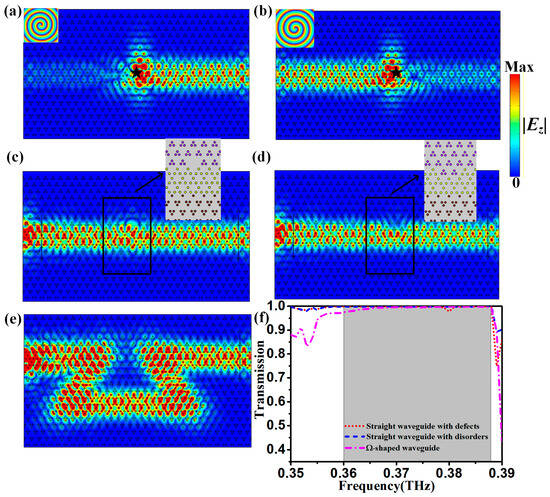
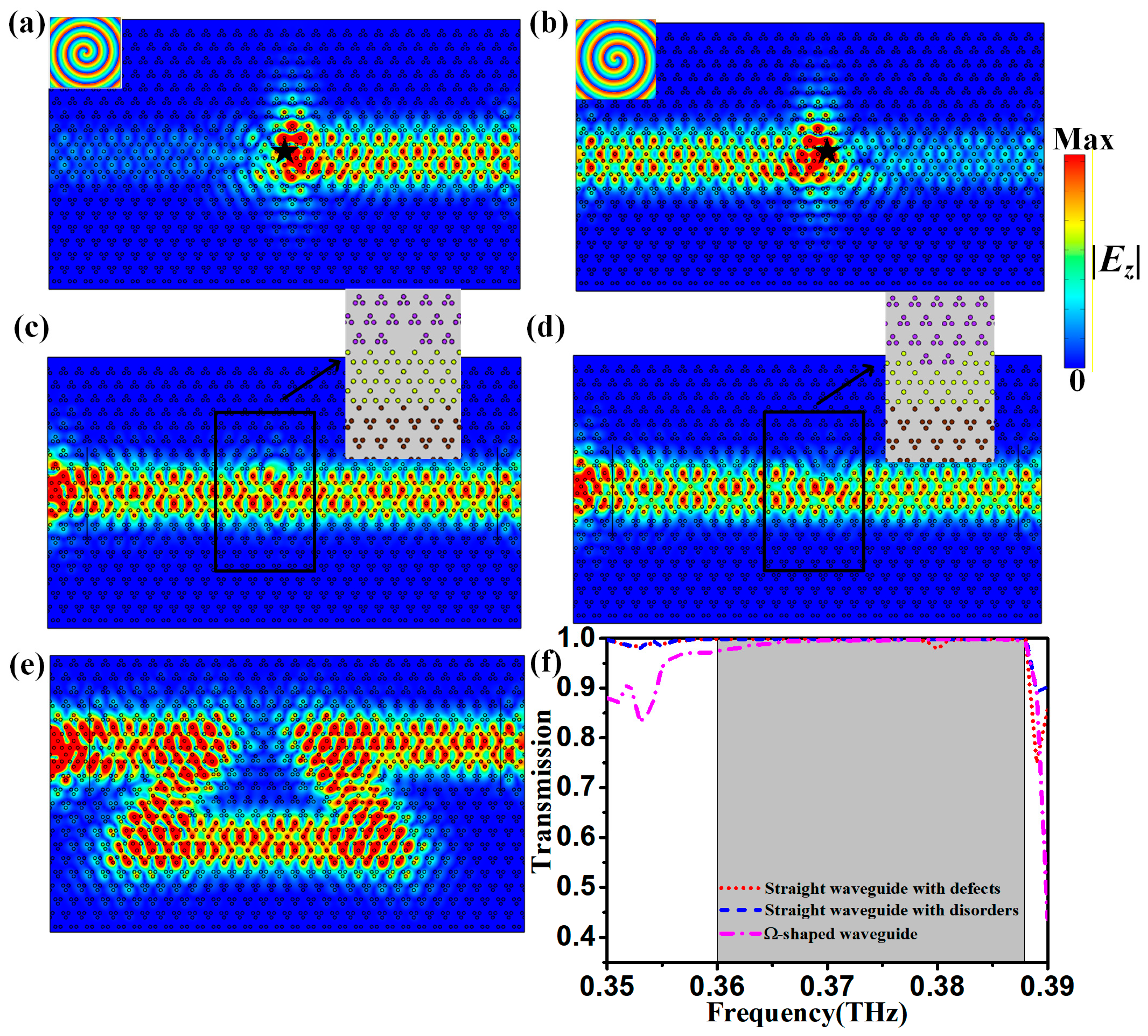
To validate the valley-momentum locking property of topological large-area waveguide states, a straight sandwich-structured waveguide with AB3C type is introduced, as illustrated in Figure 3a. A harmonic source operating at 0.378 THz is placed at the center of domain B, which consists of Dirac photonic crystals. This source comprises four line sources arranged with a π/2 phase increment in the counterclockwise direction. It carries positive orbital angular momentum (OAM), thereby exciting the valley-pseudospin-up state. As evidenced by the electric field distribution in Figure 3a, the electromagnetic wave propagates unidirectionally to the right port. Conversely, when the phase increment is set clockwise, this source carries negative OAM. As shown in Figure 3b, the valley-pseudospin-down state is excited. Consequently, the propagation direction reverses with the wave traveling unidirectionally to the left. In both cases, energy remains confined within domain B, decaying rapidly in the ±y directions. These results confirm both the unidirectionality and valley-momentum locking of the topological large-area waveguide states.
Figure 3.
(a,b) Straight waveguide schematic and simulated electric field intensity distributions when excited by a chiral RCP and LCP source, respectively, placed at the center (denoted by a black star) and operating at 0.378 THz. (c,d) Straight waveguide with introduced defects/disorders and the corresponding electric field distributions of the topological large-area waveguide states at 0.368 THz; insets detail the defect/disorder structures. (e) Schematic of an Ω-shaped waveguide and its simulated field distribution at 0.368 THz. (f) Simulated transmission spectra for the waveguide paths in (c–e), with the photonic bandgap indicated by the gray region.
The valley-momentum locking mechanism endows the proposed topological waveguide with high robustness, maintaining stable propagation even in the presence of defects, disorder, and sharp bends. To evaluate its robustness against imperfections, a straight waveguide containing deliberate defects or disorder is investigated. Removing one unit cell from domain B (Figure 3c, inset) causes only local disturbance, the field quickly recovers its original profile. Similarly, replacing two PC1 cells with PC2 cells (Figure 3d, inset) does not impede transmission, with consistent field distribution throughout. As illustrated in Figure 3e, an Ω-shaped waveguide with four sharp bends is also constructed. Excited by a chiral source with 0.368 THz from the left input, waves propagate through bends with negligible backscattering, consistent with the high transmission shown in Figure 3f. These results confirm that the large-area waveguide states (0.360–0.385 THz) are topologically protected and highly robust to bending. The transmission spectra in Figure 3f show near-ideal efficiency (100%) over the 0.360–0.385 THz band under lossless conditions. In electromagnetic simulations, material losses of this magnitude can typically be safely neglected, allowing high-resistivity silicon to be approximated as a lossless medium. The actual transmission loss will primarily originate from radiation or reflection inherent in the structure itself. Therefore, the high transmission efficiency and robust immunity to bends, defects, and disorder confirm that the heterostructure waveguide supports large-area, topologically protected propagating modes.
5. Topological Large-Area Corner States
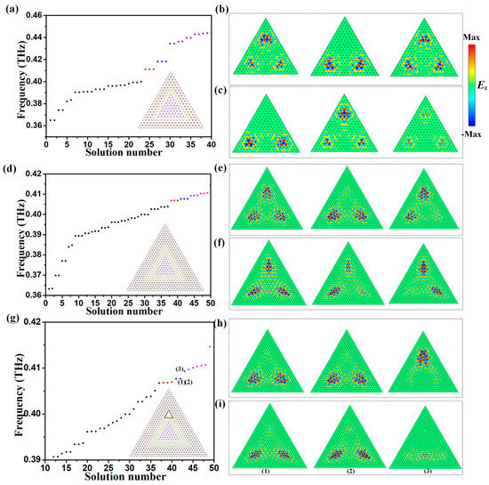
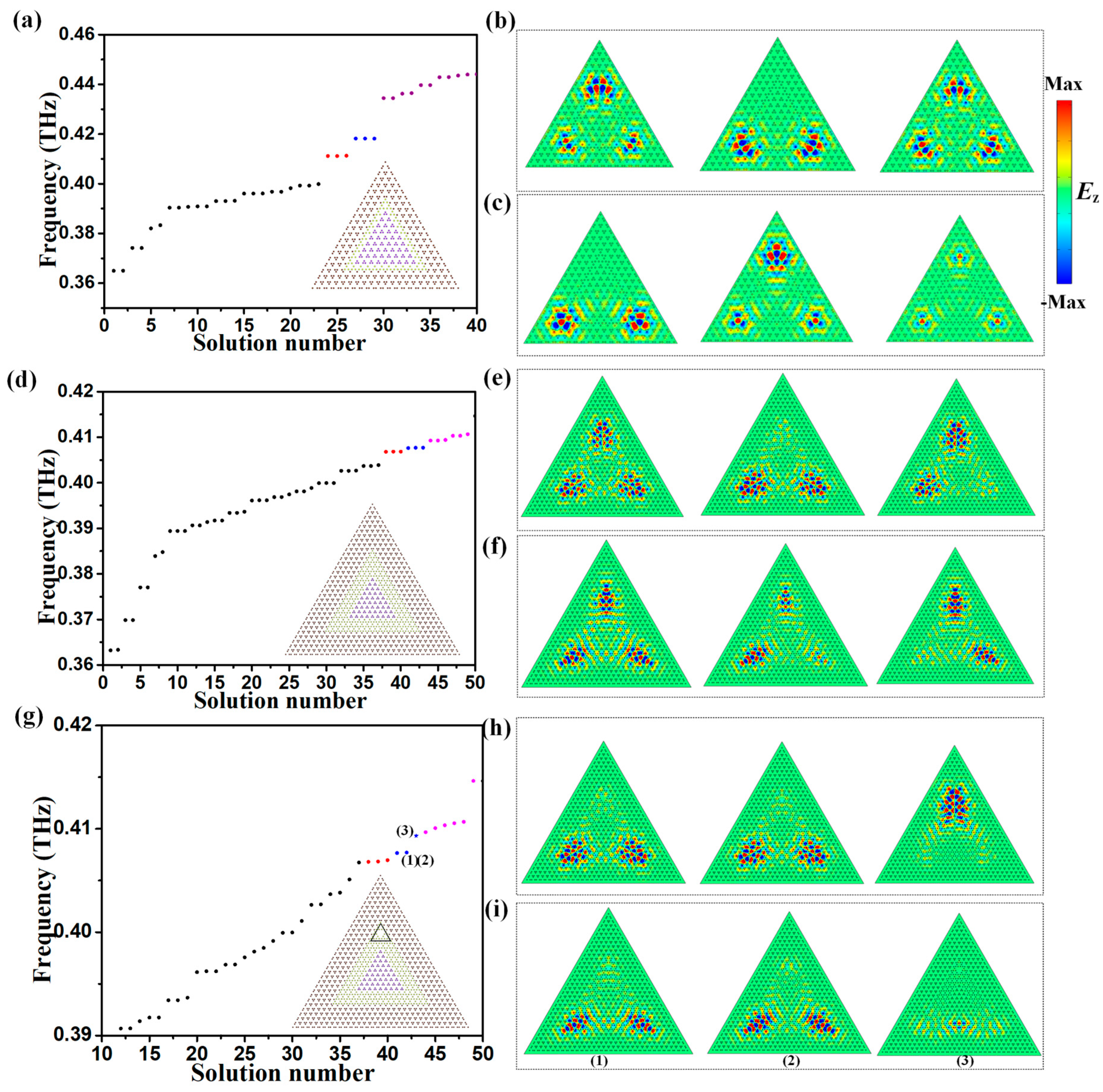
Numerous studies have demonstrated that topological corner states can exist at the intersection of trivial and non-trivial photonic crystals [26,27,28,29,30,31,32,33,34,35]. Similar to photonic crystals with C4 symmetry in square lattices [26,27], kagome-structured photonic crystals with C3 symmetry can also achieve zero-dimensional topological corner states in triangular box-type configurations [28,29,30]. In general, corner states are typically located within the bandgap that separates bulk and edge states, and can be independently excited and detected. The band structure of the ABC-type supercell reveals the existence of gapped waveguide states. The band gap between the topological waveguide states and bulk states may give rise to second-order topological corner states. To verify the presence of such corner states, we construct a triangular box-shaped structure, in which domain B (denoted by the yellow) composed of Dirac photonic crystals is arranged between domain A and domain C, as depicted in Figure 4a. When analyzing the eigenstates by COMSOL Multiphysics software 5.5, perfectly matched layer boundaries are applied around the entire structure. The eigenfrequencies of this structure are depicted in Figure 4b, where the black dots denote the bulk modes, the red and blue dots denote waveguide states, and the purple dots denote bulk states. There are two pairs of near-degenerate corner states. The working frequency is near 0.4112 THz and 0.4182 THz, respectively. Figure 4b shows the field distributions of corner states near the frequency with 0.4112 THz. And Figure 4c shows the field distributions of corner states near the frequency with 0.4182 THz. For conventional higher-order topological corner states, the energy is typically highly confined around a small area near the domain walls. From Figure 4b,c, we can find that the electric fields are strongly confined around a large area at the corners of the triangular domain between domain A and domain C, while the energy is predominantly localized within domain B. Furthermore, an AB3C-type supercell is constructed within a triangular box-type configuration, as illustrated in Figure 4d. The corresponding eigen frequencies are presented in the same figure, where black dots represent bulk modes and red dots denote waveguide states. Two pairs of near-degenerate corner states are observed, with operating frequencies located approximately at 0.4068 THz and 0.4076 THz, respectively. Their field distributions are displayed in Figure 4e,f. Compared with the ABC-type supercell, the corner states here exhibit energy confinement over a significantly larger area. It is demonstrated that these types of corner structures with heterostructures can support large-area corner states. However, among the two sets of corner states observed in Figure 4a,d, only the red dots represent topological corner states. This identification is confirmed by the quantized bulk polarization∣P∣ = 1/3 obtained from Wilson loop calculations, which is consistent with theoretical prediction for higher-order topological corner states in valley photonic crystals. In contrast, the blue dots represent trivial corner states arising from boundary truncation effects. They lack topological protection, as evidenced by their sensitivity to local perturbations. This distinction aligns with the fundamental principle that the topological invariant in this system can only induce one set of topological corner states via the bulk-edge correspondence.
Figure 4.
(a) A combined ABC-type triangle box-shaped structure and the eigen frequencies of the combined structure. (b,c) Simulated electric field distributions of the corner states corresponding to the eigenmodes denoted by red and blue dots in (a), respectively. (d) Another combined triangle box-shaped structure with AB3C-type and the eigen frequencies of the combined structure. (e,f) Simulated electric field distributions of the corner states corresponding to the eigenmodes denoted by red and blue dots in (d), respectively. (g) Combined triangle box-shaped structure with AB3C-type with a local defect indicated by a black triangular and the eigen frequencies of the combined structure. (h) Simulated electric field distributions of the corner states corresponding to the eigenmodes denoted by red dots with frequency near 0.4068 THz in (g). (i) Simulated electric field distributions of the eigenmodes denoted by blue dots in (1), (2); eigenmode in (3) is a trivial corner state with the frequency of 0.4077 THz.
To validate this property for the corner states observed in our system, we introduce controlled geometric perturbations near the corners. As depicted in Figure 4g, a local defect indicated by a black triangular is implemented by removing three pillars within the structure. The calculated eigen frequencies for the defective configuration are shown in Figure 4g. The frequency of corner states denoted by the red dots shifts from 0.4068 THz to 0.4069 THz. The results reveal that the corner states remain robust against the perturbation, exhibiting only minor frequency shifts. This robustness is further supported by the field distributions presented in Figure 4h, which exhibit persistent energy confinement at the corners despite the presence of the defect. Simulated electric field distributions of trivial corner states are shown in Figure 4i. The modes marked by (1)(2) with the frequency of 0.4077 THz exhibit persistent energy confinement at the corners. In contrast, the corner state denoted by (3) exhibits a significant frequency drift, shifting from 0.4077 THz to 0.4093 THz, and corner states ultimately vanish completely. Furthermore, to facilitate comparison, the effective mode area is calculated for both the large-area corner states presented and conventional corner states. The effective mode area Aeff is defined based on the energy distribution as follows:
This formula provides a measure of the spatial extent of the mode, independent of a subjective threshold [43]. For the AC-type supercell constructed within a triangular boundary configuration, the operating frequency of the topological corner state is approximately 0.4054 THz. According to Equation (1), the corresponding effective mode area is calculated to be Aeff = 6.115 × 10⁻⁷ m2. For the ABC-type supercell, the operating frequency of the topological corner state is approximately 0.4112 THz, with an effective mode area of Aeff = 8.368 × 10⁻⁷ m2. For the AB3C-type supercell, the operating frequency of the topological corner state is approximately 0.4068 THz, yielding an effective mode area of Aeff = 2.630 × 10⁻⁶ m2. This quantitative comparison shows that the mode area of corner states of AB3C-type is more than 4.3 times larger than that of conventional corner states with the ABC-type supercell. Therefore, it is evident that increasing the number of Dirac material layers revealing Dirac-like dispersion can effectively enlarge the modal area of topological higher-order corner modes. The strongly localized optical field characteristics of such topological large-area corner states can render them suitable for applications in laser resonators. By combining large-area mode confinement with reduced optical loss, this strategy provides a viable pathway toward realizing low-threshold, high-stability topological lasers.
6. Computational Details
A variety of numerical techniques have been developed in recent years for modeling optical and photonic systems. In terms of computational algorithms, there are some major algorithms, including optimization algorithms, numerical simulation algorithms, and physical analysis algorithms [44,45,46,47]. Reference [44] combined the cultural algorithm with rigorous coupled-wave analysis (RCWA) and finite-difference time-domain (FDTD) approach for inverse design. The reported work [45] proposed an inverse design framework for guided-mode resonance (GMR) filters by combining rigorous coupled-wave analysis (RCWA) and global optimization. Reference [46] improved simulation accuracy and efficiency using the Dirichlet-to-Neumann (DtN) boundary integral method. The reported work [47] employed multipolar expansion to identify resonance origins. Together, these algorithms form a complete technical chain from optimization and simulation to physical analysis. They will provide new ideas and methods for the design of intelligent topological electromagnetic devices.
However, all numerical simulations presented in this work are performed using COMSOL Multiphysics 5.5 with the finite element method (FEM). The eigenvalue problem derived from Maxwell’s equations is solved in the frequency domain to extract the photonic band dispersions. Periodic boundary conditions are enforced at the unit cell boundaries, with Floquet periodicity applied to sample the wavevectors along the high-symmetry contours of the irreducible Brillouin zone. Edge state calculations are conducted using supercell configurations. In these simulations, perfectly matched layers (PMLs) are placed at the upper and lower boundaries to eliminate unwanted reflections, while periodic conditions are retained along the direction parallel to the domain wall. A non-uniform meshing scheme with adaptive refinement is adopted to ensure numerical convergence; specifically, the maximum mesh element size was set to λ/10 in dielectric materials and λ/20 in air regions to capture fine field distributions accurately. To investigate the emergence of corner states, we construct a finite-size triangular supercell consisting of an inner triangular domain (occupied by PC1) surrounded by an outer annular domain (occupied by PC2). During eigenmode analysis, perfectly matched layer (PML) boundaries are applied around the entire structure to emulate an open boundary condition and suppress spurious reflections.
7. Discussions and Conclusions
Although this study is based on numerical simulations, the proposed terahertz photonic crystal configuration is experimentally feasible. A viable fabrication route involves the use of photolithographic patterning followed by dry etching. Specifically, a high-resistivity silicon substrate coated with a photoresist is exposed via UV or electron-beam lithography [48]. Subsequent reactive ion etching (RIE) transfers the pattern into the silicon, yielding the periodic pillar lattice [49]. Upon removal of the residual photoresist, a metallic layer is deposited on the reverse side of the substrate, thereby establishing a boundary condition conducive to vertical wave confinement.
A detailed comparison of our work with previously reported topological large-area waveguide states is provided in Table 1. Previous articles have primarily focused on realizing topological large-area waveguide states in valley photonic crystals or metasurfaces [37,40,41,42], but have not investigated topological large-area corner states. Our work, based on the valley Hall effect in a Kagome lattice, achieves valley-momentum locking by adjusting the cylinder spacing. It not only investigates the robust transmission of topological large-area waveguide states but also delves into the mode area expansion characteristics of large-area corner states, which are immune to defects. The structure is relatively simple and classic. In contrast, the previous work [50] employs a more complex petal-shaped structure constructed from three circular dielectric scatterers, forming a six-petal shape with each unit cell containing six petal-shaped scatterers. It is based on the spin Hall effect with C6 symmetry and utilizes a petal-shaped structure to realize pseudospin-momentum locking.
Table 1.
A comparison between our work and previous work with topological large-area states.
In conclusion, we propose a THz topological photonic crystal featuring a three-layer heterostructure based on a Kagome lattice. The configuration consists of a Dirac photonic crystal layer sandwiched between two distinct topological photonic crystal layers. This heterostructural design enables the realization of large-area topological waveguide states. Numerical simulations verify that these widely distributed topological waveguide states are primarily confined within the Dirac photonic crystal layer. Furthermore, they exhibit valley-momentum locking characteristics. Notably, these states maintain robust transmission even in the presence of structural defects and sharp bends. Additionally, the structure supports topological large-area corner states, which are localized at the heterojunction interfaces and display strong spatial confinement. Compared with conventional topological corner states, the heterostructure design substantially expands the modal area, thereby enhancing energy capacity. These findings provide a foundational technological pathway for advancing next-generation terahertz systems, including high-speed communication platforms, ultra-sensitive sensors, and quantum light sources.
Author Contributions
Methodology, Y.Z. and J.L.; software, Y.Z. and J.H.; validation, H.H., J.L. and X.G.; writing—original draft preparation, Y.Z. All authors have read and agreed to the published version of the manuscript.
Funding
This work was supported by the Open Foundation of Key Laboratory of Multi-spectral Absorbing Materials and Structures, Ministry of Education (KPKFJJ20260011-4), Nature Science Foundation of Chengdu Aeronautic Polytechnic University (ZZX0624081), and China Postdoctoral Science Foundation (2024M764271).
Data Availability Statement
Data are contained within the article.
Conflicts of Interest
The authors declare no conflicts of interest.
References
- Ozawa, T.; Price, H.M.; Amo, A.; Goldman, N.; Hafezi, M.; Lu, L.; Rechtsman, M.C.; Schuster, D.; Simon, J.; Zilberberg, O.; et al. Topological photonics. Rev. Mod. Phys. 2019, 91, 015006. [Google Scholar] [CrossRef] [Scilit]
- Ma, S.; Anlage, S.M. Microwave applications of photonic topological insulators. Appl. Phys. Lett. 2020, 116, 250502. [Google Scholar] [CrossRef] [Scilit]
- Lan, Z.; Chen, M.L.N.; Gao, F.; Zhang, S.; Sha, W.E.I. A brief review of topological photonics in one, two, and three dimensions. Rev. Phys. 2022, 9, 100076. [Google Scholar] [CrossRef] [Scilit]
- Haldane, F.D.M.; Raghu, S. Possible realization of directional optical waveguides in photonic crystals with broken time-reversal symmetry. Phys. Rev. Lett. 2008, 100, 013904. [Google Scholar] [CrossRef] [Scilit]
- Wang, Z.; Chong, Y.D.; Joannopoulos, J.D.; Soljačić, M. Reflection-free one-way edge modes in a gyromagnetic photonic crystal. Phys. Rev. Lett. 2008, 100, 013905. [Google Scholar] [CrossRef] [Scilit]
- Khanikaev, A.B.; Mousavi, S.H.; Tse, W.K.; Kargarian, M.; MacDonald, A.H.; Shvets, G. Photonic topological insulators. Nat. Mater. 2013, 12, 233–239. [Google Scholar]
- Wu, L.H.; Hu, X. Scheme for achieving a topological photonic crystal by using dielectric material. Phys. Rev. Lett. 2015, 114, 223901. [Google Scholar] [CrossRef] [Scilit]
- Barik, S.; Miyake, H.; DeGottardi, W.; Waks, E.; Hafezi, M. Two-dimensionally confined topological edge states in photonic crystals. New J. Phys. 2016, 18, 035013. [Google Scholar] [CrossRef] [Scilit]
- Yang, Y.; Xu, Y.F.; Xu, T.; Wang, H.X.; Jiang, J.H.; Hu, X.; Hang, Z.H. Visualization of a unidirectional electromagnetic waveguide using topological photonic crystals made of dielectric materials. Phys. Rev. Lett. 2018, 120, 217401. [Google Scholar] [CrossRef] [Scilit]
- Ma, T.; Shvets, G. All-Si valley-Hall photonic topological insulator. New J. Phys. 2016, 18, 025012. [Google Scholar]
- Chen, X.D.; Zhao, F.L.; Chen, M.; Dong, J.W. Valley-contrasting physics in all-dielectric photonic crystals: Orbital angular momentum and topological propagation. Phys. Rev. B 2017, 96, 020202. [Google Scholar]
- Gao, Z.; Yang, Z.; Gao, F.; Xue, H.; Yang, Y.; Dong, J.; Zhang, B. Valley surface-wave photonic crystal and its bulk/edge transport. Phys. Rev. B 2017, 96, 201402. [Google Scholar]
- Wu, X.; Meng, Y.; Tian, J.; Huang, Y.; Xiang, H.; Han, D.; Wen, W. Direct observation of valley-polarized topological edge states in designer surface plasmon crystals. Nat. Commun. 2017, 8, 1304. [Google Scholar] [CrossRef] [Scilit] [PubMed]
- He, X.-T.; Liang, E.-T.; Yuan, J.-J.; Qiu, H.-Y.; Chen, X.-D.; Zhao, F.-L.; Dong, J.-W. A silicon-on-insulator slab for topological valley transport. Nat. Commun. 2019, 10, 872. [Google Scholar] [CrossRef] [Scilit]
- Yang, Y.; Yamagami, Y.; Yu, X.B.; Pitchappa, P.; Webber, J.; Zhang, B.; Fujita, M.; Nagatsuma, T.; Singh, R. Terahertz topological photonics for on-chip communication. Nat. Photonics 2020, 14, 446–451. [Google Scholar] [CrossRef] [Scilit]
- Gong, Y.; Wong, S.; Bennett, A.J.; Huffaker, D.L.; Oh, S.S. Topological insulator laser using valley-Hall photonic crystals. ACS Photonics 2020, 7, 2089–2097. [Google Scholar] [CrossRef] [Scilit]
- Zeng, Y.; Chattopadhyay, U.; Zhu, B.; Qiang, B.; Li, J.; Jin, Y.; Li, L.; Davies, A.G.; Linfield, E.H.; Zhang, B.; et al. Electrically pumped topological laser with valley edge modes. Nature 2020, 578, 246–250. [Google Scholar] [CrossRef] [Scilit]
- Liu, X.; Zhao, L.; Zhang, D.; Gao, S. Topological cavity laser with valley edge states. Opt. Express 2022, 30, 4965–4977. [Google Scholar] [CrossRef] [Scilit]
- Cheng, Q.; Wang, S.; Lv, J.; Liu, N.H. Topological photonic crystal biosensor with valley edge modes based on a silicon-on-insulator slab. Opt. Express 2022, 30, 10792–10801. [Google Scholar]
- Kumar, A.; Gupta, M.; Pitchappa, P.; Wang, N.; Fujita, M.; Singh, R. Terahertz topological photonic integrated circuits for 6G and beyond: A perspective. J. Appl. Phys. 2022, 132, 140901. [Google Scholar] [CrossRef] [Scilit]
- Kumar, A.; Gupta, M.; Pitchappa, P.; Wang, N.; Szriftgiser, P.; Ducournau, G.; Singh, R. Phototunable chip-scale topological photonics: 160 Gbps waveguide and demultiplexer for THz 6G communication. Nat. Commun. 2022, 13, 4090. [Google Scholar] [CrossRef] [Scilit] [PubMed]
- Li, B.L.; Shi, H.Y.; Sha, W.E.I.; Yi, J.J.; Li, G.Q.; Zhang, A.X.; Xu, Z. Valley topological line-defects for terahertz waveguides and power divider. Opt. Mater. 2022, 126, 112196. [Google Scholar] [CrossRef] [Scilit]
- Han, J.; Liang, F.; Huang, D.; Zhao, Y.; Liu, J.; Zhao, D.; Wang, B.Z. Topological traveling-wave radiation based on chiral edge states in photonic Chern insulators. Opt. Lett. 2024, 49, 5877–5880. [Google Scholar] [CrossRef] [Scilit] [PubMed]
- Fan, X.; Zhou, B. Anti-scattering propagation in multiple-bend valley phononic crystals. New J. Phys. 2024, 26, 053009. [Google Scholar] [CrossRef] [Scilit]
- Banerjee, R.; Kumar, A.; Tan, T.C.; Gupta, N.; Jia, R.; Szriftgiser, P.; Ducournau, G.; Chong, Y.; Singh, R. On-chip amorphous terahertz topological photonic interconnects. Sci. Adv. 2025, 11, eadu2526. [Google Scholar] [CrossRef] [Scilit]
- Kim, M.; Jacob, Z.; Rho, J. Recent advances in 2D, 3D and higher-order topological photonics. Light Sci. Appl. 2020, 9, 130. [Google Scholar] [CrossRef] [Scilit]
- Xie, B.Y.; Wang, H.F.; Wang, H.X.; Zhu, X.Y.; Jiang, J.H.; Lu, M.H.; Chen, Y.F. Second-order photonic topological insulator with corner states. Phys. Rev. B 2018, 98, 205147. [Google Scholar] [CrossRef] [Scilit]
- Xie, B.Y.; Su, G.X.; Wang, H.F.; Su, H.; Shen, X.P.; Zhan, P.; Lu, M.H.; Wang, Z.L.; Chen, Y.F. Visualization of higher-order topological insulating phases in two-dimensional dielectric photonic crystals. Phys. Rev. Lett. 2019, 122, 233903. [Google Scholar] [CrossRef] [Scilit]
- Li, M.; Zhirihin, D.; Gorlach, M.; Ni, X.; Filonov, D.; Slobozhanyuk, A.; Alù, A.; Khanikaev, A.B. Higher-order topological states in photonic kagome crystals with long-range interactions. Nat. Photonics 2020, 14, 89–94. [Google Scholar] [CrossRef] [Scilit]
- Shao, S.; Liang, L.; Hu, J.H.; Poo, Y.; Wang, H.X. Topological edge and corner states in honeycomb-kagome photonic crystals. Opt. Express 2023, 31, 18375–18386. [Google Scholar] [CrossRef] [Scilit]
- Shen, K.; Deng, W.M.; Mo, H.C.; Shi, F.L.; Ma, F.; Chen, X.D.; Dong, J.W. Observation of robust edge mode and in-gap corner mode in kagome surface-wave photonic crystals. Opt. Lett. 2023, 48, 2973–2976. [Google Scholar] [CrossRef] [Scilit] [PubMed]
- Li, M.; Liu, Y.; Du, L.; Li, P.; Dong, Y.; Tao, L.; Li, Z.; Li, D.; Lu, L.; Chang, L. Ultrabroadband valley transmission and corner states in valley photonic crystals with dendritic structure. Commun. Phys. 2024, 7, 99. [Google Scholar] [CrossRef] [Scilit]
- Chen, X.D.; Deng, W.M.; Shi, F.L.; Zhao, F.L.; Chen, M.; Dong, J.W. Direct observation of corner states in second-order topological photonic crystal slabs. Phys. Rev. Lett. 2019, 122, 233902. [Google Scholar] [CrossRef] [Scilit] [PubMed]
- Wang, H.-X.; Liang, L.; Jiang, B.; Hu, J.; Lu, X.; Jiang, J.-H. Higher-order topological phases in tunable C3 symmetric photonic crystals. Photon. Res. 2021, 9, 1854–1864. [Google Scholar]
- He, Y.-H.; Gao, Y.-F.; He, Y.; Qi, X.-F.; Si, J.-Q.; Yang, M.; Zhou, S.-Y. Realization of edge and corner states in photonic crystals with kagome lattices through topological insulator generators. Opt. Laser Technol. 2023, 161, 109150. [Google Scholar] [CrossRef] [Scilit]
- Song, S.; Zhang, L. Detailed analysis of topological edge and corner states in valley-Hall-like photonic kagome insulators. Appl. Phys. B 2024, 130, 41. [Google Scholar]
- Wang, M.D.; Zhou, W.Y.; Bi, L.Y.; Geng, Z.G.; Liu, X.J.; Peng, Y.G.; Zhu, X.F.; Liu, J.; Lu, M.H. Valley-locked waveguide transport in acoustic heterostructures. Nat. Commun. 2020, 11, 3000. [Google Scholar] [CrossRef] [Scilit]
- Wang, J.Q.; Zhang, Z.D.; Yu, S.Y.; Peng, Y.G.; Liu, X.J.; Lu, M.H. Extended topological valley-locked surface acoustic waves. Nat. Commun. 2022, 13, 1324. [Google Scholar] [CrossRef] [Scilit]
- Chen, Z.Y.; Wang, X.Y.; Lim, C.W.; Chen, J.T.; Lu, M.H. Robust large-area elastic transverse wave transport in active acoustic metamaterials. J. Appl. Phys. 2022, 131, 185112. [Google Scholar] [CrossRef] [Scilit]
- Wang, M.; Zhang, R.; Zhang, L.; Wang, D.; Guo, Q.; Zhang, Z.; Chan, C.T. Topological one-way large-area waveguide states in magnetic photonic crystals. Phys. Rev. Lett. 2021, 126, 067401. [Google Scholar] [CrossRef] [Scilit]
- Chen, Q.; Zhang, L.; Chen, F.; Yan, Q.; Xi, R.; Chen, H.; Yang, Y. Photonic topological valley-locked waveguides. ACS Photonics 2021, 8, 1400–1406. [Google Scholar] [CrossRef] [Scilit]
- Yan, S.; Zhao, D.; Yang, Y.H.; Zhang, B.L. Transport of a topologically protected photonic waveguide on-chip. Photonics Res. 2023, 11, 1021–1028. [Google Scholar] [CrossRef] [Scilit]
- Li, Z.; Li, S.; Yan, B.; Chan, H.-C.; Li, J.; Guan, J.; Bi, W.; Xiang, Y.; Gao, Z.; Zhang, S.; et al. Symmetry-Related Large-Area Corner Mode with a Tunable Mode Area and Stable Frequency. Phys. Rev. Lett. 2025, 134, 116607. [Google Scholar] [CrossRef] [Scilit] [PubMed]
- Khorrami, Y.; Fathi, D.; Rumpf, R.C. Fast Optimal Design of Optical Components Using the Cultural Algorithm. Opt. Express 2020, 28, 15954–15968. [Google Scholar] [CrossRef] [Scilit] [PubMed]
- Khorrami, Y.; Fathi, D.; Rumpf, R.C. Guided-mode resonance filter optimal inverse design using one- and two-dimensional grating. J. Opt. Soc. Am. B-Opt. Phys. 2020, 37, 425–432. [Google Scholar] [CrossRef] [Scilit]
- Demeester, T.; De Zutter, D. Quasi-TM Transmission Line Parameters of Coupled Lossy Lines Based on the Dirichlet to Neumann Boundary Operator. IEEE Trans. Microw. Theory Tech. 2008, 56, 1649–1660. [Google Scholar] [CrossRef] [Scilit]
- Maleki, J.; Fathi, D. Refractive Index Sensor Based on Fano-Magnetic Toroidal Quadrupole Resonance Enabled by Bound State in the Continuum in All-Dielectric Metasurface. Sci. Rep. 2024, 14, 4110. [Google Scholar] [CrossRef] [Scilit]
- Karimi, K.; Fardoost, A.; Mhatre, N.; Rajan, J.; Boisvert, D.; Javanmard, M. A Thorough Review of Emerging Technologies in Micro- and Nanochannel Fabrication: Limitations, Applications, and Comparison. Micromachines 2024, 15, 1274. [Google Scholar] [CrossRef] [Scilit]
- Miyata, K.; Toyoshima, L.; Iijima, K.; Goto, Y.; Shohmitsu, Y.; Wada, T.; Nakaoka, T. Terahertz bandpass filter with Babinet complementary metamaterial mirrors and silicon subwavelength structure. Optics Express 2023, 31, 23507–23517. [Google Scholar] [CrossRef] [Scilit]
- Zhao, Y.; Liang, F.; Li, J.; Han, J.; Chen, J.; Hu, H.; Zhang, K.; Yang, Y. Topological Large-Area Waveguide States Based on THz Photonic Crystals. Photonics 2025, 12, 791. [Google Scholar] [CrossRef] [Scilit]

Disclaimer/Publisher’s Note: The statements, opinions and data contained in all publications are solely those of the individual author(s) and contributor(s) and not of MDPI and/or the editor(s). MDPI and/or the editor(s) disclaim responsibility for any injury to people or property resulting from any ideas, methods, instructions or products referred to in the content. |
© 2026 by the authors. Licensee MDPI, Basel, Switzerland. This article is an open access article distributed under the terms and conditions of the Creative Commons Attribution (CC BY) license.