


Abstract
Diamond exhibits outstanding stability and broadband spectral transparency, rendering it an ideal material for optical windows in extreme environments. Antireflective structures such as pyramids and nano-stripes serve as the prevailing strategy for further enhancing window transmittance. However, their fabrication is often hindered by the inherent trade-off between processing quality and efficiency. Herein, we propose a scalable method combining spatial beam shaping with orthogonal scanning via femtosecond laser to fabricate sub-wavelength structures (laser-induced periodic surface structures, LIPSS) on diamond for infrared antireflective windows. The line focus formed by a cylindrical lens substantially enlarges the effective processing area, increasing the area processed per unit time by more than a factor of ten and thus enhancing the processing efficiency. High-quality 2D-LIPSS were successfully fabricated by integrating orthogonal scanning with wet etching and show a transmittance of 76–78%. In contrast, 1D-LIPSS only improved the transmittance to approximately 72%. This work demonstrates for the first time that diamond LIPSS can achieve antireflective effects in the 8–12 μm long-wave infrared band, providing an effective solution to balance surface quality with processing efficiency and offering a promising route for the practical application of diamond infrared windows.
1. Introduction
Infrared optical windows are critical components of infrared imaging and detection systems. They are required to achieve functions such as transmitting target signals and providing protection [1]. Applications in extreme environments pose severe challenges for infrared optical windows, including intense aerodynamic heating, high-pressure shock, and particle erosion experienced by hypersonic vehicles flying at Mach numbers, high-energy laser irradiation in high-power laser systems, and prolonged seawater erosion and chemical corrosion during deep-sea exploration [2,3,4], imposing stringent requirements on optical window materials. Compared to conventional infrared window materials such as ZnS, ZnSe, and sapphire, diamond demonstrates superior comprehensive material properties [5,6]. It exhibits broadband transparency from visible to microwave regimes, ultra-high hardness and thermal conductivity, and exceptional chemical stability [7,8]. However, its high refractive index (n = 2.4) causes a severe index mismatch at the diamond–environment interface, limiting its transmittance in the infrared region to only about 70% [9]. Typical solutions rely on depositing antireflective coatings onto the diamond surface via chemical vapor deposition (CVD) or physical vapor deposition (PVD) to enhance transmittance by creating a refractive index gradient layer between the air and the diamond [10,11]. However, severe thermal mismatch at the interface between the thin-film coating and the diamond in extreme conditions can lead to coating failure, which undermines the intrinsic environmental stability of diamond [12,13]. Inspired by biological features like moth eyes, directly patterning sub-wavelength features onto the material provides a robust, coating-free alternative for antireflection [14,15].
The physical and chemical stability of diamond poses a significant challenge for the fabrication of antireflective structures. Mechanical machining [16] and electrical discharge machining [17] struggle to meet the processing precision required for antireflective structures. While electron beam lithography (EBL) [18] and reactive ion etching (RIE) [19] enable high-precision fabrication, they suffer from complex processes, prohibitive costs, and low processing efficiency. Characterized by extremely high peak power and ultra-short pulse duration, femtosecond lasers offer high processing precision and material versatility, driving their widespread application in micro/nanofabrication [20,21,22,23]. This provides an effective method for fabricating diamond-based infrared optical windows. For instance, femtosecond laser direct writing assisted by gas flow and laser cleaning have been employed to create sub-wavelength antireflective arrays on diamond, achieving enhanced transmittance in the 8–12 μm range [24,25]. However, given that morphological features strictly dictate optical performance, point-by-point scanning method typically creates only a single grating groove per scan, requiring multiple back-and-forth scans to create high aspect ratio antireflective structures, which inherently limits the processing efficiency [26,27]. Laser-induced periodic surface structures (LIPSS) enable the single-step fabrication of self-organized nano-grating patterns. They are used to create functional surfaces with properties such as anti-reflectivity, structural color, and self-cleaning capabilities [28,29,30,31]. Previous studies have utilized femtosecond lasers to fabricate various types of LIPSS on diamond, successfully enhancing transmittance in the visible and near-infrared regimes. E. Granados et al. used ultraviolet femtosecond lasers to directly fabricate LIPSS with a 400 nm period on diamond. Simulations indicated a theoretical transmittance approaching 100% at a wavelength of 1.25 μm [32]. Furthermore, techniques such as multi-beam parallel processing and beam shaping have introduced novel approaches for enhancing manufacturing efficiency [33]. For example, Cao et al. utilized a cylindrical lens for beam shaping to fabricate one-dimensional LIPSS (1D-LIPSS) with a 100 nm period on diamond using femtosecond lasers. This method enabled the successful processing of a 12 × 24 µm2 area in just 3 s, demonstrating that the structures could increase visible-light transmittance to 76% [34]. M. Mastellone et al. employed temporal shaping techniques to create deep-sub-wavelength columnar LIPSS with an 80 nm period on diamond using two time-delayed, cross-polarized femtosecond laser beams. Although the reflectance of these structures in the 400–1000 nm range dropped from 33% to 8%, their concurrently high absorptance renders them unsuitable for optical window applications [35]. However, the exploration of diamond LIPSS is predominantly confined to short-wavelength applications, leaving a critical gap in the 8–12 μm range.
Here, we propose a scalable method combining spatial beam shaping and femtosecond laser orthogonal scanning to fabricate antireflective structures on diamond for infrared antireflective windows. The linear beam profile shaped by a cylindrical lens significantly expands the effective processing area. This expansion increases the processed area per unit time by more than a factor of ten, thereby improving the processing efficiency by more than an order of magnitude. We integrated orthogonal scanning with wet etching to fabricate high-quality two-dimensional LIPSS (2D-LIPSS). Notably, the 2D-LIPSS exhibit an average transmittance of 76–78% in the 8–12 μm range, whereas the 1D-LIPSS only increase the transmittance to approximately 72%. This work offers an effective solution to balance the surface quality and processing efficiency, paving the way for the practical application of diamond infrared windows.
2. Materials and Methods
2.1. Materials and Processing Parameters
The antireflective structure was fabricated on a 4 mm × 4 mm × 0.3 mm monocrystalline diamond substrate. The femtosecond laser (YSL Photonics, Wuhan, China) was employed, working at a central wavelength of 1030 nm, a repetition rate of 25 kHz and a pulse duration of 375 fs. The polarization was adjusted by rotating a half-wave plate (HWP), whereas the laser fluence was precisely controlled using a neutral density filter. The incident laser beam was shaped into a linear spot by inserting a cylindrical lens prior to the objective (40×/0.75) to improve the processing efficiency. To achieve high-precision fabrication of micro/nanostructures, this system employs an XM ultra-precision linear motor stage (Newport Corporation, Irvine, CA, USA) as the 3D motorized platform. Featuring a 50 mm travel range, a maximum velocity of 300 mm/s, and a minimum incremental motion of 1 nm, this stage satisfies the rigorous requirements for precise displacement control.
2.2. Processing Strategy
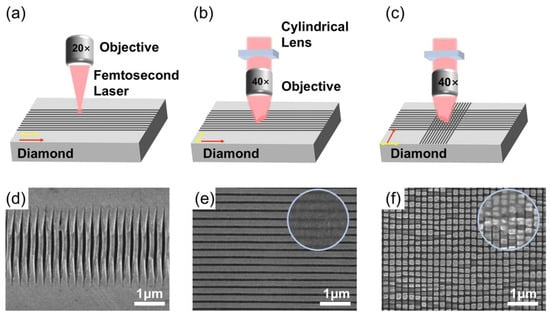
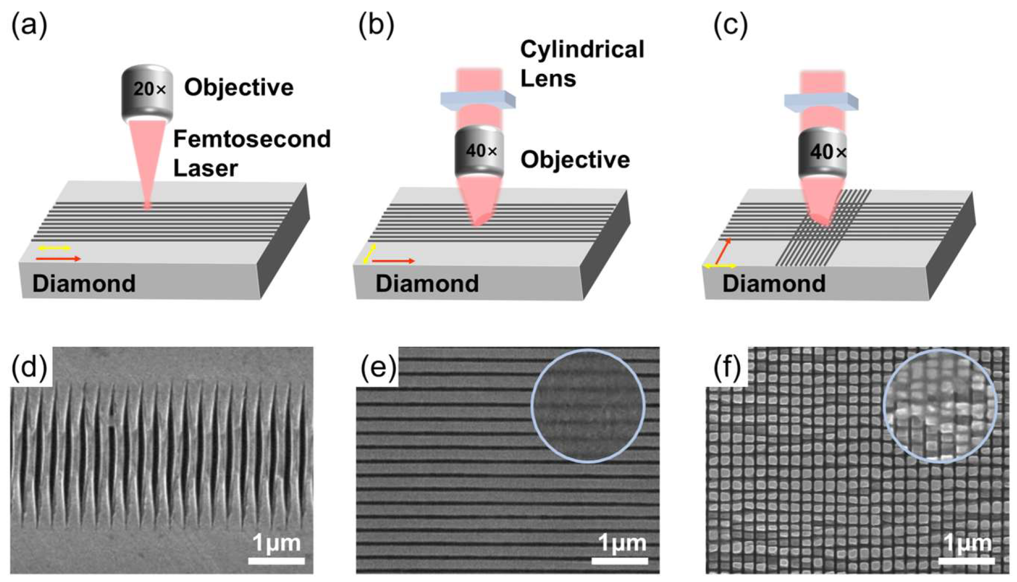
Conventional single-point femtosecond laser processing to prepare antireflective LIPSS requires multiple scans (Figure 1a). The inconsistent light intensity at the center and edge of the Gaussian beam leads to a decrease in structure uniformity (Figure 1d). Moreover, due to the limited size of the laser beam, the processing efficiency can only reach mm2/h. Due to its one-dimensional curvature and orthogonal planar geometry, a cylindrical lens selectively converges the laser wavefront along a single axis. The laser beam was shaped by the cylindrical lens, transforming the Gaussian spot into a spot with a linear energy distribution (Figure 1b). In contrast to the rapid energy decay along the short axis of the Gaussian focus (radius of ~0.56 µm), the decay along the long axis (1/e2 half-width of ~150 μm) of the line focus is significantly more gradual as simulated in Supplementary Figure S1. This results in minimal variation in the accumulated dose across the scanned band, creating optimal conditions for the formation of high-quality LIPSS (Figure 1b,e). Given that the LIPSS orientation aligns perpendicular to the laser polarization, the laser polarization direction was oriented perpendicular to the current scan path. This specific arrangement mitigates the stitching artifacts caused by the non-uniform energy distribution of the spot. As a result, the fabricated 1D-LIPSS exhibit high uniformity (Figure 1e).
Figure 1.
Fabrication strategies and resulting structures. (a) Point scanning of a focused Gaussian spot. (b) Line scanning with a cylindrical lens. (c) 2D-LIPSS formed by a second line scan perpendicular to the first. (d–f) SEM images of the structures in (a–c), respectively; the insets in (e,f) show the structures before etching. Yellow and red arrows denote the laser polarization and scanning directions, respectively.
The 2D-LIPSS antireflective structures were fabricated via an orthogonal scanning strategy (Figure 1c). Specifically, setting the laser polarization perpendicular to the initial scanning direction yields 1D-LIPSS with ripples aligned parallel to the scan path. Subsequently, a second scan is executed orthogonally to the pre-formed 1D-LIPSS ripples. By maintaining the polarization perpendicular to this second scanning direction, the initial one-dimensional structures are periodically segmented, thereby forming 2D-LIPSS. This approach transforms the 1D-LIPSS into a 2D sub-wavelength structure (Figure 1f). To remove the laser-induced graphite and amorphous carbon that obscure the underlying structures (insets of Figure 1e,f), the wet etching process was employed. The laser-processed samples were immersed in a mixture of concentrated nitric acid (HNO3) and sulfuric acid (H2SO4) at a 1:8 volume ratio and maintained at 80 °C for 8 h. Ultrasonic cleaning of the sample was performed in deionized water to remove detached residues.
2.3. Characterization
Field-emission scanning electron microscopy (FE-SEM) was utilized to characterize the structure. Atomic force microscopy (AFM) was employed to evaluate the surface roughness and extract structural parameters. Raman spectroscopy was utilized to verify the structural integrity of the diamond and confirm the effective removal of impurities. The optical properties of both the 1D- and 2D-LIPSS in the 8–12 μm wavelength were assessed using a Fourier transform infrared (FTIR) spectrometer.
3. Results
3.1. Fabrication of 1D-LIPSS
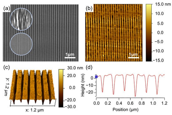
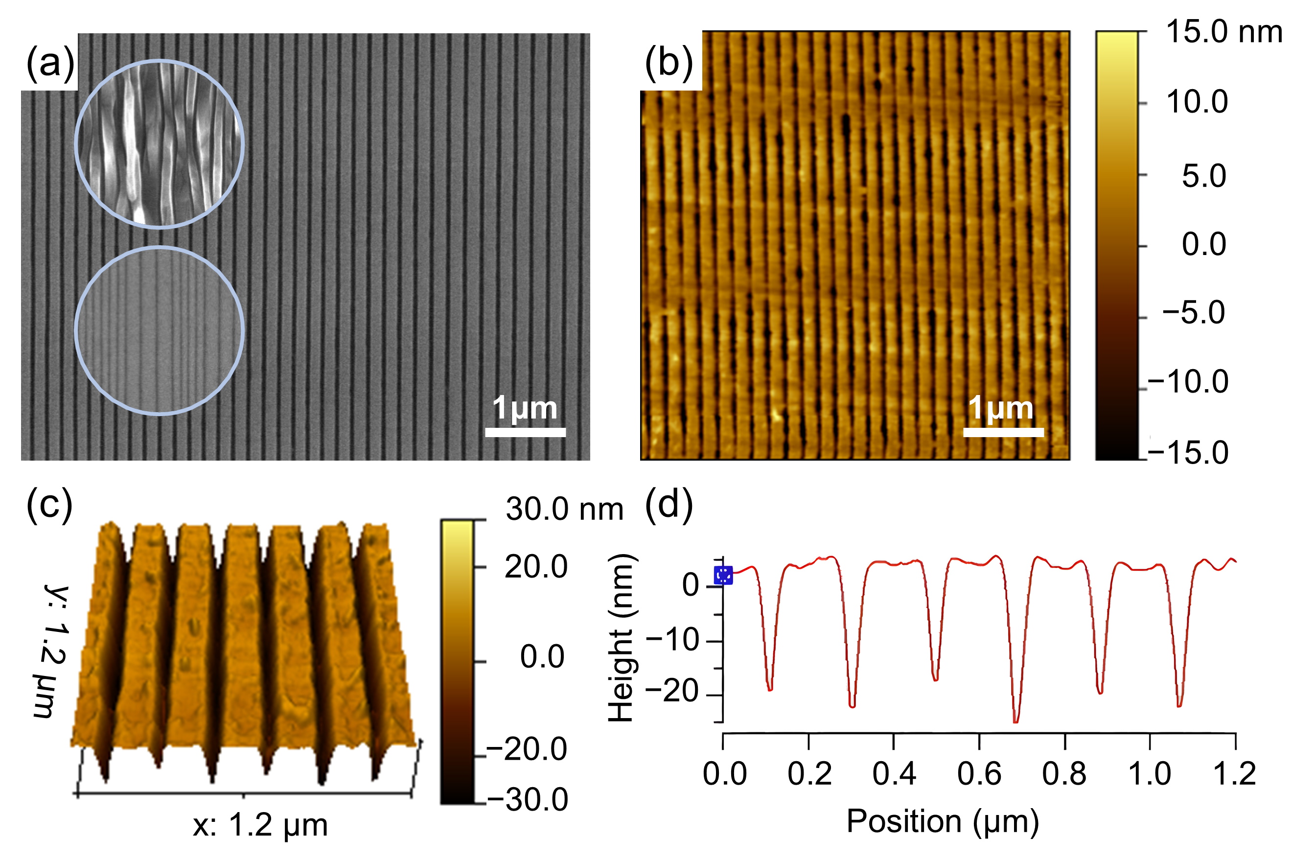
The 1D-LIPSS were fabricated using a cylindrical lens to reshape the incident laser into a linear focal spot. The femtosecond laser (1030 nm wavelength) induced LIPSS with a spatial period of 200 nm, satisfying the structural requirements for infrared (8–12 μm) antireflective. Following the Sipe scattering–interference model, this periodicity originates from the interference of the incident beam with waves scattered by inherent surface roughness. This interaction drives a spatially periodic energy deposition dictated by the wavelength and the dielectric constant [36]. Structural morphology is highly sensitive to the scanning speed and laser power. SEM images of the structures obtained at a fixed scanning speed for different laser fluences, and at a fixed fluence for different scanning speeds, are given in Supplementary Figure S2. At low laser fluence near the modification threshold, only shallow and discontinuous ripples form [37]. As the fluence reaches an optimal regime, the LIPSS become highly straight and uniform with sharp edges and no resolidified debris. Conversely, excessive fluence triggers thermodynamic instability and dominant ablation, which disrupts the surface plasmon interference field and results in severe ripple bifurcation with chaotic melt deposition. Furthermore, scanning speed governs the pulse overlap essential for LIPSS evolution. Low speeds cause excessive thermal accumulation that destroys the gratings, whereas high speeds lead to insufficient overlap and structural fragmentation. High speed with low powers leads to discontinuous ripples (near-threshold regime, Figure 2a inset). Conversely, low speeds with high power cause massive over-ablation (ablation damage regime). Figure S3 also shows SEM images of large-area LIPSS produced by a single line scan. At excessive laser fluence, the central region of the scanned track (across the short axis) is damaged by ablation and differs markedly from the edges, whereas a moderate power yields uniform LIPSS over the whole scanned area. Employing moderate scanning speeds and laser powers consistently yields well-defined and uniform LIPSS morphologies, representing the optimal processing regime.
Figure 2.
(a) SEM image of the 1D-LIPSS fabricated at 0.1 mm/s and 8.47 J/cm2; the upper inset shows the near-threshold regime and the lower inset shows the ablation damage regime. (b) AFM topography of (a). (c) Three-dimensional morphological map corresponding to the AFM measurement. (d) Cross-sectional profile extracted from (c).
As illustrated in Figure 2a, following systematic parameter optimization, the scanning speed and laser fluence were finalized at 0.1 mm/s and 8.47 J/cm2, respectively. After the wet etching process, high-quality 1D-LIPSS were obtained. SEM images reveal highly straight, uniformly periodic ripples with sharp trench edges and no obvious resolidified melt accumulation. This confirms that the applied pulse accumulation and energy density perfectly align with the optimal LIPSS induction regime. The samples were further characterized using atomic force microscopy (AFM). Both the 2D and 3D morphological maps (Figure 2b,c) demonstrate excellent parallelism and structural uniformity. Chemical etching effectively removed the amorphous carbon residues that previously obscured the trench morphology. This post-treatment significantly reduced sidewall roughness and minimized potential light scattering losses. Cross-sectional profile analysis (Figure 2d) indicates that the ripples exhibit a shallow U-shaped micro-trench morphology. The average structural period remains highly stable at approximately 200 nm. Crucially, the beam-shaping strategy circumvents the severe structural disorder at stitching seams and the over-ablation typically associated with conventional point-scanning methods. This approach enables the fabrication of large-area, high-quality 1D-LIPSS through only single scanning, increasing the processing efficiency by more than a factor of ten through the enlargement of the processed area per unit time.
3.2. Fabrication and Characterization of 2D-LIPSS
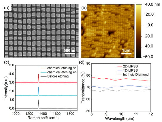
The 2D-LIPSS were fabricated by conducting a secondary orthogonal scan, and the direction of the second scan was perpendicular to that of the first. The laser polarization was set perpendicular to the current scanning direction. The line-shaped beam ablates across the initial grating ripples, transforming the 1D grating into a 2D square-mesa array. Following the laser processing, localized variations in surface roughness, optical absorptivity, and defect density emerge, which trigger pronounced laser-induced effects during the second pass. To avoid structural damage, the incident laser fluence was reduced to 6.65 J/cm2 while the scanning speed was kept 0.1 mm/s. As shown in Figure 3a, a 2D square-mesa array was formed with regular morphology and a highly consistent spatial period. The structures exhibit well-defined edges without obvious melt re-solidification or material spallation. AFM characterization over a 5 × 5 μm2 area reveals that the 2D-LIPSS form a closed packed, highly ordered array with excellent in-plane spatial uniformity (roughness of only 7 nm) (Figure 3b). Following the 8 h wet etching process, Raman spectroscopy was used to confirm the removal of laser-induced graphite and amorphous carbon debris (Figure 3c), evidenced by the absence of the D-peak and G-peak. The characteristic diamond peak at 1332 cm−1 exhibited no significant frequency shift. This indicates that the ultrafast laser processing caused no substantial structural damage, fully preserving the single-crystal diamond lattice within the 2D-LIPSS array.
Figure 3.
(a) SEM image of the fabricated 2D-LIPSS. (b) AFM image of the fabricated 2D-LIPSS. (c) Raman spectra of 2D-LIPSS under various etching durations. (d) FTIR transmission spectra of pristine diamond, 1D-LIPSS, and 2D-LIPSS.
Fourier transform infrared (FTIR) transmission spectra in the 8–12 μm band exhibit flat profiles without resonance dips for pristine diamond, 1D-LIPSS, and 2D-LIPSS, confirming the sub-wavelength nature of the induced structures (Figure 3d). Compared to the 67–68% transmittance of pristine diamond, the 1D-LIPSS only improve the average transmittance to about 72%. This modest enhancement of approximately 4% reflects the limited antireflection performance of the 1D-LIPSS in this band. In contrast, the 2D-LIPSS achieves a transmittance of approximately 76–78% across the entire band. This represents a roughly 10% enhancement over pristine diamond. These results validate this strategy as a highly efficient and robust pathway for manufacturing high-performance infrared windows.
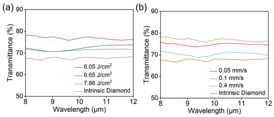
To further study the influence of the processing parameters on the structure and optical properties of 2D-LIPSS, samples were fabricated at different laser fluences and scanning speeds. The surface morphologies are shown in Figure S4; when the laser fluence of the second scan is close to or slightly below the modification threshold, material is removed only from the ridges of the 1D grating and the energy reaching the bottom of the grooves is too low for a complete orthogonal cut. Consequently, no isolated 2D array forms, and the transmittance (~72%) stays close to that of the 1D structure. At excessive fluence, enhanced local heat accumulation generates thermal stresses that exceed the fracture strength of diamond, so that the beam not only removes the intended material but also causes large-area spalling of the pre-formed pillars; the transmittance gain is thereby further weakened (Figure 4a). At a low scanning speed (0.05 mm/s), the increased pulse overlap raises the thermal load, and some pillars detach owing to thermal damage; although the transmittance reaches ~75%, the optimal antireflective performance is still not attained. At a high scanning speed (0.4 mm/s), the number of effective pulses is far below that required for LIPSS formation, only a shallow and irregular grid forms, which provides weak antireflection (Figure 4b). Ultimately, highly uniform 2D-LIPSS arrays are realized only under moderate fluence and scanning speed, delivering a pronounced transmittance enhancement of approximately 10% relative to the pristine diamond.
Figure 4.
FTIR transmission spectra over 8–12 µm of diamond structured by 2D-LIPSS at different (a) laser fluences and (b) scanning speeds, compared with those of intrinsic diamond.
4. Discussion
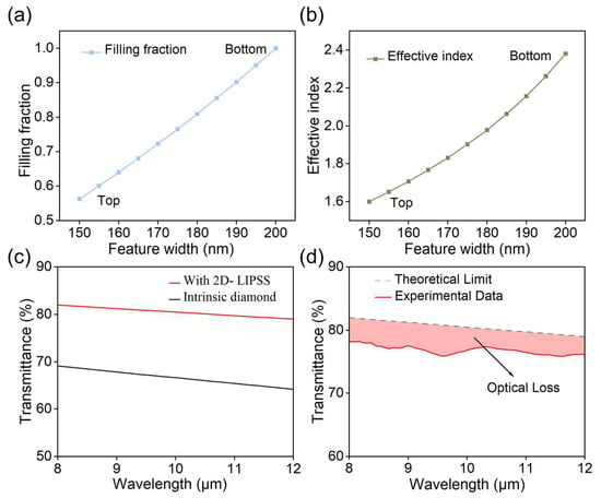
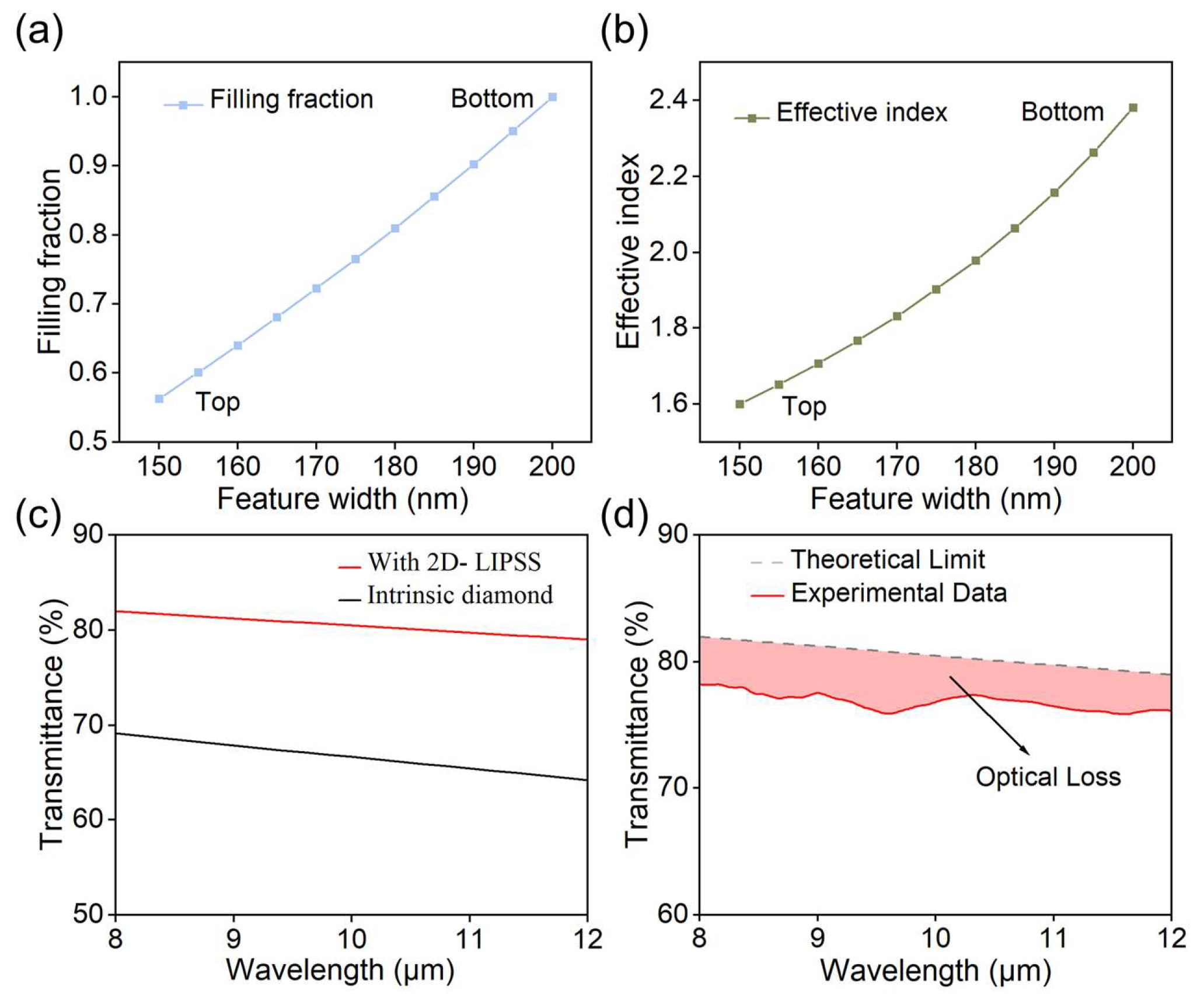
Theoretical calculations and numerical simulations were used to further verify the antireflective performance of the 2D-LIPSS in the 8–12 μm band. Optical simulations of the 2D square-mesa array were performed using the Wave Optics Module (Electromagnetic Waves, Frequency Domain interface) in COMSOL Multiphysics 6.2. The 3D computational domain consisted of a 200 nm × 200 nm unit cell containing an 800 nm air layer, a 150 nm diamond substrate (refractive index of 2.38), and the interfacial structured layer. The 2D square-mesa array is defined by its depth (H, 20 nm), period (T, 200 nm), and top edge length (L, 150 nm), in accordance with the actual fabricated structure. A free tetrahedral mesh was applied, with a maximum element size of 25 nm within the structured layer and 120 nm in the surrounding air and substrate domains. The structure was illuminated by a normally incident, x-polarized plane wave. Given the four-fold rotational symmetry of the square pillar array and its mirror symmetry under normal incidence, periodic conditions were strictly enforced using symmetry planes: perfect electric conductor (PEC) boundaries were applied at x ± T/2, and perfect magnetic conductor (PMC) boundaries at y = ±T/2. For normal incidence on a symmetric unit cell, this approach is rigorously equivalent to Floquet periodic boundary conditions. Based on effective medium theory (EMT) and the zero-order diffraction approximation, the antireflective structures act as a continuous equivalent medium layer [38]. Here, the material filling fraction f(z) is defined as the ratio of the structural cross-sectional area to the total unit cell area (Equation (1)). The side width W(z) of the square-mesa varies linearly with depth (z), as described by Equation (2). The refractive index experiences a minor initial jump at the top and then gradually approaches that of diamond at the bottom (Figure 5a). This continuous profile creates an optical buffer layer that effectively suppresses interfacial reflection.
Figure 5.
(a) Structural fill factor and (b) effective refractive index as functions of the structural lateral width. (c) Simulated transmission spectra of the pristine diamond substrate and the 2D-LIPSS. (d) Comparison between the theoretical and experimental transmission spectra of the 2D-LIPSS.
As shown in Figure 4b, the effective refractive index transitions smoothly from the top of the structure to the diamond substrate at the bottom in the 8–12 μm wavelength range (Figure 5b). This relationship can be described using volume averaging or Maxwell–Garnett approximations. Under the first-order approximation, the equivalent refractive index at any given depth is expressed by Equation (3). Based on this gradient profile, the calculated transmittance of the 2D-LIPSS in the 8–12 µm band is approximately 79–82%, which is in good agreement with the experimentally measured transmittance (Figure 5c).
As shown in Figure 5d, the 2D-LIPSS array still exhibits a minor 3–4% discrepancy compared to the theoretical transmittance. This minor discrepancy stems from residual optical losses: partial light scattering caused by inevitable nanoscale surface roughness, and infrared absorption from trace amorphous carbon phases potentially trapped in deep micro-trenches. Nevertheless, the diamond 2D-LIPSS array fabricated via orthogonal line-scanning demonstrates remarkable broadband antireflection performance. Compared with previous studies using femtosecond lasers to fabricate antireflective structures on diamond for the 8–12 μm band, this work achieves comparable transmittance enhancement while offering substantially higher processing efficiency (Table 1). This methodology provides an efficient and robust means of developing high-performance, high-damage-threshold antireflective windows for high-power infrared laser systems.
Table 1.
Comparison of different fabrication methods for antireflective structures on diamond.
5. Conclusions
We have developed a highly efficient technique for fabricating diamond infrared windows using a beam-shaping femtosecond laser. Highly uniform 1D-LIPSS and 2D-LIPSS with excellent surface quality were fabricated via an orthogonal scanning strategy. The optical transmittance of the 2D-LIPSS in the 8–12 μm band demonstrates enhancement to 76–78%, while the average transmittance of 1D-LIPSS is only about 72%. Compared to pristine diamond, the average transmittance increased by approximately 10%. In contrast to the previous study using a femtosecond laser to fabricate antireflective structures on diamond for the 8–12 µm band, this work achieves a comparable transmittance while offering a superior processing efficiency. Ultimately, this beam-shaping ultrafast processing technique offers a highly scalable and robust pathway for manufacturing diamond optical windows tailored for extreme environments. Furthermore, this study establishes a comprehensive theoretical and experimental framework for realizing broadband infrared antireflection in other advanced optical materials.
Supplementary Materials
The following supporting information can be downloaded at: https://www.mdpi.com/article/10.3390/photonics13111089/s1, Figure S1: (a) Simulated energy distribution of the line-shaped beam. (b) Energy distribution profile along the long axis of the line focus. (c) Energy distribution profile along the short axis of the line focus; Figure S2: SEM images of 1D-LIPSS fabricated at a fixed scanning speed of 0.1 mm/s with laser fluences of (a) 7.86, (b) 8.47, (c) 9.10 and (d) 9.68 J/cm2, and at a fixed fluence of 6.65 J/cm2 with scanning speeds of (e) 0.05, (f) 0.1, (g) 0.2 and (h) 0.4 mm/s; Figure S3: (a) SEM image of a large-area structure produced by a single line-focus scan at 0.1 mm/s and 9.68 J/cm2; (b) magnified view of (a). (c) SEM image of a large-area structure produced by a single line-focus scan at 0.1 mm/s and 8.47 J/cm2; (d) magnified view of (c); Figure S4: SEM images of 2D-LIPSS fabricated at a fixed scanning speed of 0.1 mm/s with fluences of (a) 6.05, (b) 6.65, (c) 7.26 and (d) 7.82 J/cm2, and at a fixed fluence of 6.65 J/cm2 with scanning speeds of (e) 0.05, (f) 0.1, (g) 0.2 and (h) 0.4 mm/s.
Author Contributions
Conceptualization, R.Z., J.-W.T., G.W. and Y.D.; methodology, R.Z. and J.-W.T.; software, D.L.; validation, J.-W.T. and Z.W.; formal analysis, R.Z. and D.L.; investigation, R.Z. and D.L.; resources, G.W. and Y.D.; data curation, D.L.; writing—original draft preparation, R.Z.; writing—review and editing, R.Z. and J.-W.T.; visualization, R.Z.; supervision, J.-W.T., G.W., Y.D., Z.B., Y.W. and Z.L.; project administration, G.W. and Y.D.; funding acquisition, G.W. and Y.D. All authors have read and agreed to the published version of the manuscript.
Funding
This work was supported by the Opening Funding of National Key Laboratory of Electromagnetic Space Security.
Data Availability Statement
The data that support the findings of this study are available within the paper and Supplementary Materials. Additional data related to this paper are available from the corresponding authors upon reasonable request.
Conflicts of Interest
The authors declare no conflicts of interest.
References
- Bushunov, A.A.; Tarabrin, M.K.; Lazarev, V.A. Review of surface modification technologies for mid-infrared antireflection microstructures fabrication. Laser Photonics Rev. 2021, 15, 2000202. [Google Scholar] [CrossRef] [Scilit]
- Yi, S.; Ding, H.L.; Luo, S.; Sun, X.B.; Xia, Z. Research progress on aero-optical effects of hypersonic optical window with film cooling. Light Sci. Appl. 2024, 13, 310. [Google Scholar] [CrossRef] [Scilit]
- Zhang, C.X.; Zhang, L.; Zhang, H.; Fu, B.; Wang, J.Y.; Qiu, M. Pulsed polarized vortex beam enabled by metafiber lasers. PhotoniX 2024, 5, 36. [Google Scholar] [CrossRef] [Scilit]
- Ding, Y.; Jiang, X.; Wang, C.; Jia, X.; Liu, L.; Han, W.; Gao, Z.; Wang, S.; Lin, N.; Yan, D.; et al. Femtosecond laser rapid customization of high-performance anti-reflection windows. Opto-Electron. Sci. 2026, 5, 260004. [Google Scholar] [CrossRef] [Scilit]
- Chang, X.Y.; Gao, W.X.; An, J.S.; Chen, H.; Liu, Z.T.; Qi, Z.H.; Li, C.W.; Ding, J.; Li, W.L.; Wang, K. Optical-grade diamond: Characteristics, synthesis, and recent research progress. Funct. Diam. 2025, 5, 2476690. [Google Scholar] [CrossRef] [Scilit]
- Guillemet, R.; Lee, M.-S.L.; Jussey, D.; Traouli, E.; Loiseaux, B.; Garabédian, P.; Khemis, S.B.; Scorsone, E.; Rossi, E.; Rashid, S. Multifunctional CVD diamond window for Infrared imaging. MRS Adv. 2025, 10, 1251–1258. [Google Scholar] [CrossRef] [Scilit]
- Gu, K.; Zhang, Z.; Zhang, Z.; Huang, J.; Koide, Y.; Koizumi, S.; Liao, M. Optical properties of single-crystal diamond MEMS: Mitigating substrate interference. Funct. Diam. 2025, 5, 2570362. [Google Scholar] [CrossRef] [Scilit]
- Zhang, F.; Li, P.; Chen, Y.; Chen, H.; Zheng, H.; Tan, B.; Wang, K.; Ding, J.; Wang, Y.; Lu, Z.; et al. A thermo–optical chain-linked model and adaptive cavity-length compensation for high-power diamond Raman lasers. High Power Laser Sci. Eng. 2026, 14, e61. [Google Scholar] [CrossRef] [Scilit]
- Dore, P.; Nucara, A.; Cannavo, D.; De Marzi, G.; Calvani, P.; Marcelli, A.; Sussmann, R.S.; Whitehead, A.J.; Dodge, C.N.; Krehan, A.J. Infrared properties of chemical-vapor deposition polycrystalline diamond windows. Appl. Opt. 1998, 37, 5731–5736. [Google Scholar] [CrossRef] [Scilit]
- Huang, Y.B.; Zhao, X.; Zhu, X.H.; Liu, S.J.; Wang, X.L.; Yue, Y.H.; Sun, W.S.; Wang, P.; Guo, X.Q.; Li, C.M. The thermal stability of Er2O3 anti-reflective films deposited on CVD diamond by magnetron sputtering. Ceram. Int. 2025, 51, 17568–17574. [Google Scholar] [CrossRef] [Scilit]
- Wang, J.G.; Feng, C.; Zhang, W.L.; Xu, Z.Y.; Liu, X.F.; Yi, K.; Shao, J.D. Hydrophobic antireflective coating with high laser damage threshold by physical vapor deposition. Mod. Phys. Lett. B 2021, 35, 2150209. [Google Scholar] [CrossRef] [Scilit]
- Yang, Y.T.; Cai, Q.Y.; Liu, D.Q.; Gao, L.S.; Zhang, H.T.; Peng, L.; Hu, E.T.; Liu, B.J.; Luo, H.H.; Zhang, R.J. Low polarization-sensitive ultra-broadband anti-reflection coatings with improved reliability. Opt. Express 2023, 31, 25477–25489. [Google Scholar] [CrossRef] [Scilit]
- Zambrano-Mera, D.F.; Espinoza-González, R.; Rosenkranz, A.; Harvey, T.J.; Polcar, T.; Valenzuela, P.; Gacitúa, W. Enhanced erosion resistance of anti-reflective TiO2/SiO2 coatings induced by Zr-oxide doping. Sol. Energy Mater. Sol. Cells 2023, 250, 112079. [Google Scholar] [CrossRef] [Scilit]
- Yang, H.T.; Pu, J.H.; Lu, L. Anti-reflective engineering via moth-eye-inspired nanostructures: Fundamental principles, fabrications, and applications. Renew. Sustain. Energy Rev. 2026, 231, 116785. [Google Scholar] [CrossRef] [Scilit]
- Liu, X.Q.; Zhang, Y.L.; Li, Q.K.; Zheng, J.X.; Lu, Y.M.; Juodkazis, S.; Chen, Q.D.; Sun, H.B. Biomimetic sapphire windows enabled by inside-out femtosecond laser deep-scribing. PhotoniX 2022, 3, 1. [Google Scholar] [CrossRef] [Scilit]
- Liu, Q.; Li, Q.; Zhou, X.Q.; Liu, Z.W.; Lu, M.M. Fabrication of anti-reflective surfaces by 3-DOF fast tool servo diamond turning. Int. J. Adv. Manuf. Technol. 2018, 95, 2875–2883. [Google Scholar] [CrossRef] [Scilit]
- Jiang, M.; Li, L.; Sun, X.M.; Wang, W.C.; Liu, Z.C. Research on the mechanism and process of polycrystalline diamond by EDM. Int. J. Adv. Manuf. Technol. 2023, 125, 819–830. [Google Scholar] [CrossRef] [Scilit]
- Yang-Keathley, Y.; Maloney, S.A.; Hastings, J.T. Real-time dose control for electron-beam lithography. Nanotechnology 2021, 32, 095302. [Google Scholar] [CrossRef] [Scilit]
- Sun, S.; Xu, F.; Zhou, S.J.; Shi, X.Q.; Liu, Y.; Zuo, D.W. Morphology evolution and non-uniformity removal mechanism analysis of diamond nanocone arrays by reactive ion etching. Diam. Relat. Mater. 2024, 145, 111153. [Google Scholar] [CrossRef] [Scilit]
- Wang, Z.; Zeng, F.R.; Ma, R.Z.; Tang, J.X.; Shi, M.; Qiu, J.R.; Zhang, B. 3D lithography of diamond thermal emitters for microscale emissivity control. Nat. Commun. 2026, 17, 8715. [Google Scholar] [CrossRef] [Scilit]
- Liu, Y.N.; Ding, Y.; Liu, Z.P.; Li, X.C.; Tian, S.C.; Fan, L.S.; Xie, J.C.; Xu, L.L.; Lee, J.W.; Li, J. Ultrafast laser one-step construction of 3D micro-/nanostructures achieving high-performance zinc metal anodes. PhotoniX 2024, 5, 6. [Google Scholar] [CrossRef] [Scilit]
- Cai, Y.; Fan, J.T.; Meng, F.C.; Song, Y.J.; Hu, M.L. Delayed optical feedback-regulated artificial soliton molecule in a femtosecond optical parametric oscillator. PhotoniX 2024, 5, 41. [Google Scholar] [CrossRef] [Scilit]
- Zhou, K.; Yuan, Y.P.; Wang, C.L.; Zhang, K.H.; Chen, J.M.; He, H.Y. Rapid fabrication of antireflective structures on ZnS surface by spatial shaping femtosecond laser. Opt. Laser Technol. 2024, 171, 110393. [Google Scholar] [CrossRef] [Scilit]
- Hu, Y.W.; Chen, S.T.; Kong, D.J.; Yang, M.Y.; Sun, X.Y.; Duan, J.A. Design and fabrication of subwavelength antireflective microstructures on diamond surfaces. Opt. Commun. 2025, 575, 131316. [Google Scholar] [CrossRef] [Scilit]
- Cao, H.; Li, Y.F.; Wang, G.; Li, H.Y.; Sun, D.R.; Tang, Z.Q.; Li, L.F.; Jin, Z.S.; Yu, Y.; Liu, X.Q. Laser Cleaning-Assisted Femtosecond Laser Direct Writing of Diamond Antireflective Microstructures with Superhigh Transmittance of 94.5% at 10.6 μm. Small Struct. 2025, 6, 2400590. [Google Scholar] [CrossRef] [Scilit]
- Maleki, M.J.; Soroosh, M. An ultra-fast all-optical 2-to-1 digital multiplexer based on photonic crystal ring resonators. Opt. Quantum Electron. 2022, 54, 397. [Google Scholar] [CrossRef] [Scilit]
- Rao, D.G.S.; Dubey, S.K.; Mondal, H.; Soroosh, M.; Swarnakar, S. A compact all-optical half adder with low insertion losses and a high extinction ratio using a photonic crystal structure. Opt. Quantum Electron. 2026, 58, 474. [Google Scholar] [CrossRef] [Scilit]
- Kiel, F.; Trinschek, S.; Kuchmizhak, A.; Gurevich, E.L. Colouration of diamond surfaces by laser-induced periodic surface structuring. Opt. Laser Technol. 2024, 168, 109882. [Google Scholar] [CrossRef] [Scilit]
- Zhou, K.; Yuan, Y.P.; Wang, C.L.; Han, W.N. Supra-wavelength surface structures on silicon by femtosecond laser defocus structuring for antireflection. Opt. Laser Technol. 2026, 197, 114771. [Google Scholar] [CrossRef] [Scilit]
- Exir, H.; Weck, A. Mechanism of superhydrophilic to superhydrophobic transition of femtosecond laser-induced periodic surface structures on titanium. Surf. Coat. Technol. 2019, 378, 124931. [Google Scholar] [CrossRef] [Scilit]
- Li, Z.C.; Liu, W.W.; Zhang, Y.B.; Cheng, H.; Zhang, S.; Chen, S.Q. Optical polarization manipulations with anisotropic nanostructures. PhotoniX 2024, 5, 30. [Google Scholar] [CrossRef] [Scilit]
- Granados, E.; Martinez-Calderon, M.; Gomez, M.; Rodriguez, A.; Olaizola, S.M. Photonic structures in diamond based on femtosecond UV laser induced periodic surface structuring (LIPSS). Opt. Express 2017, 25, 15330–15335. [Google Scholar] [CrossRef] [Scilit]
- Li, J.; Yan, J.; Jiang, L.; Yu, J.; Guo, H.; Qu, L. Nanoscale multi-beam lithography of photonic crystals with ultrafast laser. Light Sci. Appl. 2023, 12, 164. [Google Scholar] [CrossRef] [Scilit]
- Cao, H.; Li, Y.; Wang, G.; Zhao, G.X.; Sun, D.R.; Jin, Z.S.; Xin, B.Z.; Li, S.; Yu, Y.; Wang, Y.L. Femtosecond-laser-induced periodic surface structures on diamond with high efficiency. Chin. Opt. Lett. 2025, 23, 092201. [Google Scholar] [CrossRef] [Scilit]
- Mastellone, M.; Bellucci, A.; Girolami, M.; Serpente, V.; Polini, R.; Orlando, S.; Santagata, A.; Sani, E.; Hitzel, F.; Trucchi, D.M. Deep-subwavelength 2D periodic surface nanostructures on diamond by double-pulse femtosecond laser irradiation. Nano Lett. 2021, 21, 4477–4483. [Google Scholar] [CrossRef] [Scilit]
- Sipe, J.E.; Young, J.F.; Preston, J.S.; van Driel, H.M. Laser-induced periodic surface structure. I. Theory. Phys. Rev. B 1983, 27, 1141–1154. [Google Scholar] [CrossRef] [Scilit]
- Abdelmalek, A.; Giakoumaki, A.N.; Bharadwaj, V.; Sotillo, B.; Le Phu, T.; Bollani, M.; Bedrane, Z.; Ramponi, R.; Eaton, S.M.; Maaza, M. Morphological Study of Nanostructures Induced by Direct Femtosecond Laser Ablation on Diamond. Micromachines 2021, 12, 583. [Google Scholar] [CrossRef] [Scilit]
- Bräuer, R.; Bryngdahl, O. Design of antireflection gratings with approximate and rigorous methods. Appl. Opt. 1994, 33, 7875–7882. [Google Scholar] [CrossRef] [Scilit]

Disclaimer/Publisher’s Note: The statements, opinions and data contained in all publications are solely those of the individual author(s) and contributor(s) and not of MDPI and/or the editor(s). MDPI and/or the editor(s) disclaim responsibility for any injury to people or property resulting from any ideas, methods, instructions or products referred to in the content. |
© 2026 by the authors. Licensee MDPI, Basel, Switzerland. This article is an open access article distributed under the terms and conditions of the Creative Commons Attribution (CC BY) license.