


Abstract
Full-color holographic optical element (HOE) fabrication requires accurate spatial overlap of red, green, and blue laser beams, which is difficult to maintain with conventional free-space beam-combining systems, particularly for high-resolution near-eye displays. In this work, we propose the numerical design of a fabrication-tolerant RGB laser combiner based on a shallow-etched rib-waveguide directional coupler on a 150-nm-thick silicon nitride platform. The device is designed using supermode analysis and coupled-mode theory for operation at 450, 520, and 640 nm in the transverse-electric (TE) mode. Compared with a strip-waveguide RGB combiner, the rib-waveguide design exhibits lower sensitivity to sidewall-angle deviations: for a deviation of up to , coupled-mode-theory calculations at the blue adding stage show that the average output power decreases by 0.6%, compared with 2.5 % for the strip-waveguide design. At the nominal geometry, separate three-dimensional finite-difference time-domain simulations of the two combining stages, including input and output S-bends, predict overall red, green, and blue output powers of 97.8%, 99.6%, and 99.9%, respectively, for an optimized RGB combiner with a footprint of . The device also exhibits low sensitivity to wavelength deviations. These results demonstrate the potential of a shallow-etched rib-waveguide RGB combiner for compact, efficient, and fabrication-tolerant RGB beam combining in HOE prototyping and related multicolor optical systems.
1. Introduction
Recently, augmented-reality displays have attracted considerable attention because of the novel visual experiences they provide [1,2,3]. Various innovative products have been demonstrated, and several technologies for fabricating transparent nanofilms have been extensively investigated to enable their commercialization [4,5,6,7,8,9]. Holographic optical elements (HOEs) are attractive candidates for these applications because they offer flexible optical design using spatial light modulators (SLMs) [5,10,11] and the potential for large-scale fabrication using roll-to-roll processes [12]. However, the increasing demand for high-resolution near-eye displays requires the pixel size of HOE films to be reduced further.
For full-color HOE film prototyping, red, green, and blue lasers are commonly combined using dichroic mirrors (DMs) [13,14]. Accurate spatial alignment of the three laser spots is essential for achieving color uniformity in the fabricated film. When the pixel size is extremely small, maintaining this alignment requires a mechanically complex system and a precise detection system to verify the beam positions, thereby increasing the complexity of the overall setup.
A photonic integrated circuit (PIC) can also be used as a light combiner. Because the guided red, green, and blue beams are centered in the waveguides, the beam-alignment problem can be substantially alleviated. However, fabrication deviations can cause the realized device to differ from the nominal design. In particular, sidewall-angle deviations can significantly affect the coupling efficiency, which is the nomalized output power at the wanted waveguide.
In this work, we propose the numerical design of an RGB laser combiner based on a shallow-etched rib-waveguide directional coupler with a 150-nm-thick silicon nitride core. The design exploits wavelength-dependent coupling to combine RGB light, while the waveguide geometry and interaction length are optimized using supermode analysis and coupled-mode theory. Comparisons with strip-waveguide designs quantify the improved tolerance to sidewall-angle deviations, while three-dimensional finite-difference time-domain (FDTD) simulations evaluate the combining performance and wavelength sensitivity. By combining high output efficiency with reduced sensitivity to fabrication variations, this design offers a promising approach to compact RGB beam combining for full-color HOE prototyping and related multicolor optical systems.
2. Principle
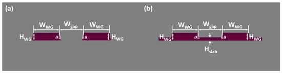
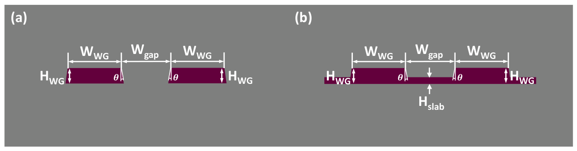
The RGB combiner employs a directional coupler (DC) to combine the three colors. By properly designing the coupler dimensions and interaction length, red, green, and blue light can be transferred into a single output channel. This approach has been used in laser-beam-scanning (LBS) systems [15,16,17,18]. The SiN layer thickness is set to 150 nm as an example, matching the thickness of the commercially available LIGENTEC AN150 platform [19]. The top and bottom cladding layers are both thicker than 3 , and visible light is generally well confined in the waveguide. Accordingly, the simulations use a 150-nm-thick waveguide of variable width embedded in a SiO2 background. A schematic of the simulated directional coupler is shown in Figure 1. The angle is defined as the deviation of the sidewall from the vertical direction; thus, perfectly vertical sidewalls correspond to . In practice, maintaining a sidewall-angle deviation close to 0 requires carefully controlled nanofabrication parameters and is generally difficult [20,21]. The effect of deviations from the ideal sidewall geometry must therefore be considered.
Figure 1.
Schematic of the simulated directional coupler. (a) Strip-waveguide directional coupler, where , , , and denote the waveguide width, gap width, total waveguide height, and sidewall-angle deviation, respectively. (b) Rib-waveguide directional coupler, where denotes the residual slab height.
A directional coupler is used to combine red, green, and blue light into a single channel. Its operating principle can be described using the propagation of two supermodes: the symmetric and antisymmetric modes [22]. The effective indices of these supermodes, and , are obtained using the Ansys Lumerical MODE solver [23]. The corresponding propagation constants are given by:
Power is completely transferred from one waveguide to the other when the two supermodes accumulate a phase difference of . Therefore, using Equation (1), the crossover length can be calculated as follows:
where .
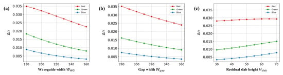
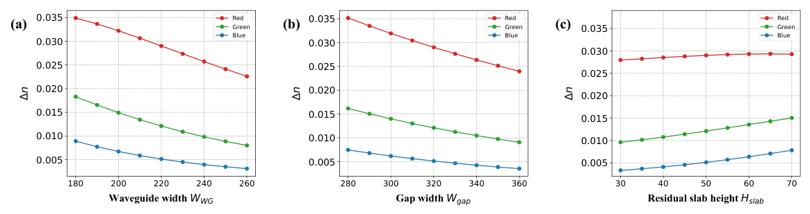
The calculated effective-index differences at the red, green, and blue wavelengths are plotted as functions of the rib-waveguide directional-coupler parameters in Figure 2. Within the investigated parameter ranges, increasing either the waveguide width or the gap width decreases , as shown in Figure 2a,b, whereas increasing the residual slab height increases , as shown in Figure 2c. Because the crossover length is given by and varies with wavelength, these structural parameters must be optimized to obtain the required wavelength-dependent coupling lengths and achieve high coupling efficiency at all three wavelengths.
Figure 2.
Dependence of the effective-index difference on the directional-coupler geometry: (a) as a function of the waveguide width , with the gap width nm and the residual slab height nm. (b) as a function of the gap width , with nm and nm. (c) as a function of the residual slab height , with nm and nm.
For a directional-coupler length L, the corresponding coupling efficiency at a given wavelength can be calculated using coupled-mode theory (CMT) [22,24,25]. Here, denotes the dimensionless cross-port power fraction and is distinct from the conventional field-coupling coefficient. The fraction of power coupled from one waveguide to the other is:
RGB combination can be realized in two steps: the green and red light are first combined, after which the blue light is added to the output channel. The combining loss in the red and green light combining stage is expected to be low and is not prioritised for directional-coupler parameter optimization. The second step is the dominant source of loss because the coupling process must selectively transfer the blue light while retaining the red and green light in their original channel. The directional-coupler parameters must therefore be optimized to minimize this loss. The RGB combiner reaches its maximum ideal efficiency when the coupling lengths satisfy ::. Even when this relation is satisfied, sidewall-angle deviations introduce additional loss. An optimized RGB combiner should therefore provide both high overall efficiency and low sensitivity to sidewall-angle deviations.
3. Design and Simulation Results
The use of a rib waveguide in the directional-coupler design may reduce the influence of sidewall-angle deviations. The partially etched structure of a rib-waveguide directional coupler mitigates the lateral geometric variations induced by sidewall-angle errors. Therefore, we first compare the sidewall-angle sensitivity of directional couplers based on strip and rib waveguides. We then design RGB combiners based on the two structures and calculate their average-output-power variation as a function of sidewall-angle deviation using coupled-mode theory. Finally, we perform three-dimensional FDTD simulations of the proposed rib-waveguide directional coupler and investigate its wavelength dependence. The RGB laser wavelengths are set to 450, 520, and 640 nm, which are commercially available. All simulations are performed using a TE-mode source.
We note here that the proposed combiner is polarization-dependent, and its geometry and interaction length are optimized for TE operation. The reported combining performance and fabrication-tolerance results therefore apply to TE-polarized excitation; equivalent performance for TM-polarized excitation has not been established in this study. In a practical implementation, all three input laser beams must be aligned with the waveguide TE polarization and maintained in this state, using lasers with a stable, fixed polarization and appropriate alignment, or polarization controllers before coupling into the chip.
3.1. Sidewall-Angle Sensitivity and Sensitivity to Other Parameters of Strip- and Rib-Waveguide Directional Couplers
To compare fabrication tolerance, we design two directional couplers based on strip and rib waveguides, respectively. Their parameters are selected to provide similar coupling lengths for 520-nm green light input, and the gap width is identical in both designs. Both structures are designed to achieve complete coupling of the 520-nm green light over a distance of approximately 21 in the TE mode. The modal effective indices are calculated using the MODE solver, from which the coupling length is obtained. The corresponding parameters are listed in Table 1.
Table 1.
Parameters of the designed strip- and rib-waveguide directional couplers. The total waveguide height is 150 nm.
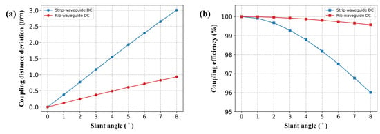
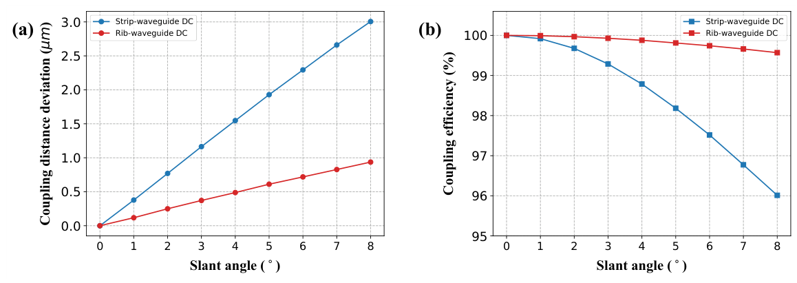
We then vary the sidewall-angle deviation of both structures from to . The gap width at the top of the waveguides remains unchanged, while the lower portions of the waveguides approach each other as the deviation increases. The coupling-length deviations of the two designs are shown as a function of in Figure 3a. As increases, the mode becomes better confined in the waveguide, resulting in a longer coupling length. The rib-waveguide DC exhibits an increase in coupling length of 0.94 , whereas the strip-waveguide DC exhibits an increase of 3.01 . The corresponding coupling-efficiency losses are shown in Figure 3b. The loss in coupling efficiency is 0.4% for the rib-waveguide DC, compared with 4.0% for the strip-waveguide DC. These results indicate that the rib-waveguide DC is more robust and less sensitive to sidewall-angle deviations during fabrication.
Figure 3.
(a) Coupling-length deviations of the rib-waveguide DC (Design 1) and strip-waveguide DC (Design 2) as functions of sidewall-angle deviation. (b) Coupling-efficiency losses of Design 1 and Design 2 as functions of sidewall-angle deviation.
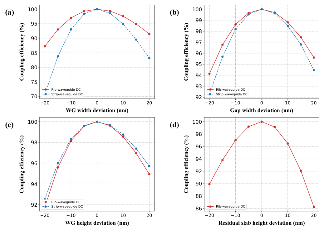
Additional individual parameter sweeps are performed to assess the sensitivity of the coupling efficiency to waveguide width, gap width, residual slab thickness, and SiN thickness (see Appendix A). For a deposition-and-partial-etch process, the total SiN thickness can be controlled during deposition, while the residual slab thickness can be adjusted by calibrating the partial-etch depth. Known systematic biases in waveguide width and gap width can be partially compensated through mask-layout adjustments after process characterization, although random dimensional variations remain. Sidewall inclination changes the cross-sectional profile throughout the etched depth, and planar dimensional compensation alone does not generally restore the intended geometry. The subsequent discussion therefore focuses on sidewall-angle deviations, consistent with the principal objective of this study: to evaluate whether a shallow-etched rib-waveguide structure can mitigate the effects of nonvertical sidewalls on RGB combining performance.
3.2. RGB Combiners and Their Sidewall-Angle Sensitivity
We design two RGB combiners based on rib and strip waveguides, respectively. To approach the target relation :: = 1:2:4, we optimize the waveguide width , gap width , and residual slab thickness for the rib-waveguide structure.
The parameters of the designed RGB combiners are listed in Table 2. The rib-waveguide RGB combiner (Design 3) is similar to Design 1 (see Table 1), but its length is set to 43.9 . The modal effective indices are extracted, and the coupling lengths at the three wavelengths are calculated. The resulting , , and are 11.03, 21.48, and 43.83 , respectively, corresponding to a ratio of 1:1.95:3.97. A similar calculation is performed for the 28.2--long strip-waveguide RGB combiner. The calculated , , and are 7.03, 13.96, and 31.98 , respectively, corresponding to a ratio of 1:1.99:4.55.
Table 2.
Parameters of the designed strip- and rib-waveguide RGB combiners. The total waveguide height is 150 nm.
In the RGB combiner, we target complete coupling of the blue light () and zero coupling of the red and green light (), so that the blue light is added to the red/green output channel. We use the average output power to evaluate the combiner performance:
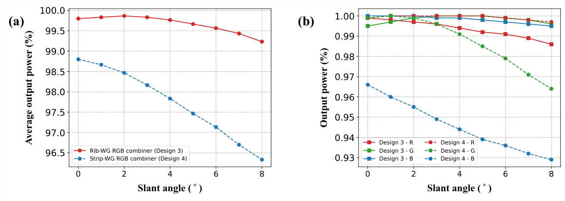
Design 3 achieves an average output power of 99.8%, with , , and . Thus, nearly all of the RGB power is successfully combined. Design 4 achieves an average output power of 98.8%, with , , and . Although the red light and green light are largely retained in the output channel, Design 4 exhibits a 3.4% loss in blue-light coupling.
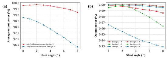
We vary the sidewall-angle deviation for both designs and plot as a function of in Figure 4a. At , the rib-waveguide RGB combiner maintains an average output power of 99.2%, with , , and . This demonstrates its low sensitivity to sidewall-angle deviations. By comparison, the strip-waveguide RGB combiner exhibits a 2.5% decrease in , with , , and . Although the strip-waveguide design remains effective, its tolerance is lower than that of the rib-waveguide design. The red, green, and blue output powers of the two designs as functions of are shown in Figure 4b; the rib-waveguide RGB combiner exhibits a smaller variation.
Figure 4.
(a) Average output power as a function of sidewall-angle deviation . The rib-waveguide RGB combiner (Design 3) is shown by the solid line, and the strip-waveguide RGB combiner (Design 4) is shown by the dashed line. (b) Red, green, and blue output powers of the two designs as functions of ; solid lines denote Design 3 and dashed lines denote Design 4.
The sidewall-angle deviations of up to considered above represent a possible case if the device fabrication is done in the laboratory and the fabrication parameters are not optimised to the maximum. Very special care needs to be taken to fabricate a device with an optimal sidewall angle and minimal sidewall roughness [20]. Sidewall-angle deviations have been reported to be approximately or less in modern commercial SiN foundry processes such as the LIGENTEC AN150 platform [19,26,27]. At , the rib-waveguide RGB combiner maintains an average output power of 99.8%, with , , and , while the strip-waveguide RGB combiner still exhibits a 0.6% decrease in , with , , and . This indicates that the proposed design tolerates the deviations expected in practical fabrication with a large margin.
3.3. FDTD Simulation and Wavelength Sensitivity of the Rib-Waveguide RGB Combiner
Before the FDTD simulations, the single-mode condition of the designed waveguide was evaluated at the three operating wavelengths using the MODE solver. For the isolated 220-nm-wide rib waveguide of Design 3, the calculation shows that only TE and TM fundamental modes are supported at 450, 520, and 640 nm (see Appendix B).
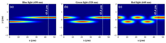
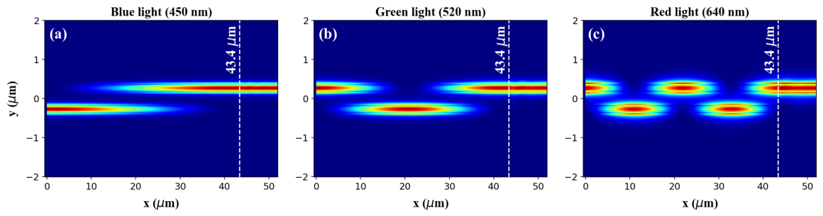
The rib-waveguide RGB combiner (Design 3) is further simulated using the Lumerical FDTD solver [28]. The FDTD simulation setup and the numerical convergence analysis are discussed in Appendix C. The simulated three-dimensional evolution of the field is shown in Figure 5. Nearly all of the blue light is coupled from one waveguide to the other, whereas the red and green light remain in the original waveguide. These results confirm effective RGB light combination.
Figure 5.
field evolution in the designed RGB combiner obtained using 3D FDTD simulations: (a) blue light (450 nm) is coupled to the other waveguide, (b) green light (520 nm) remains in the original waveguide, and (c) red light (640 nm) remains in the original waveguide.
However, the FDTD result indicates a slightly shorter optimum combiner length of 43.4 and slightly lower output powers. The corresponding RGB output powers are presented in Table 3, together with the output powers obtained from coupled-mode theory for comparison. Additional 3D FDTD simulations are carried out for sidewall-angle deviations of and , and the results confirm the low sidewall-angle sensitivity of the design, as shown in Table 3.
Table 3.
RGB output powers obtained from 3D FDTD simulations and coupled-mode theory.
We ascribe the 0.5 difference between the CMT and FDTD optimal lengths to the different levels of idealization in the two methods. The coupled-mode-theory result is obtained from two-dimensional supermode analysis, which assumes an ideal sinusoidal power exchange between the two supermodes of a uniform coupler cross-section. However, the three-dimensional FDTD simulation captures the three-dimensional evolution of the field profiles, which could possibly be responsible for the optimal length difference.
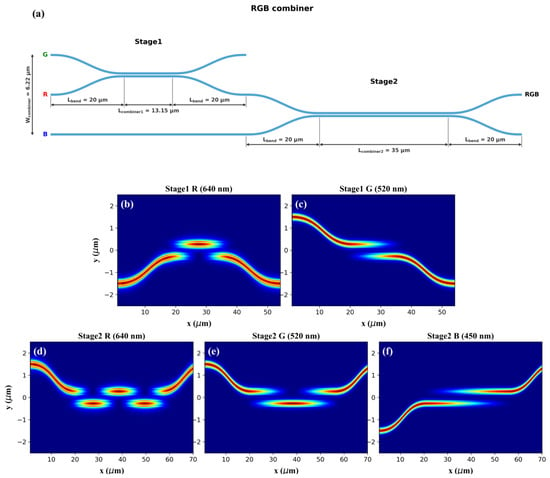
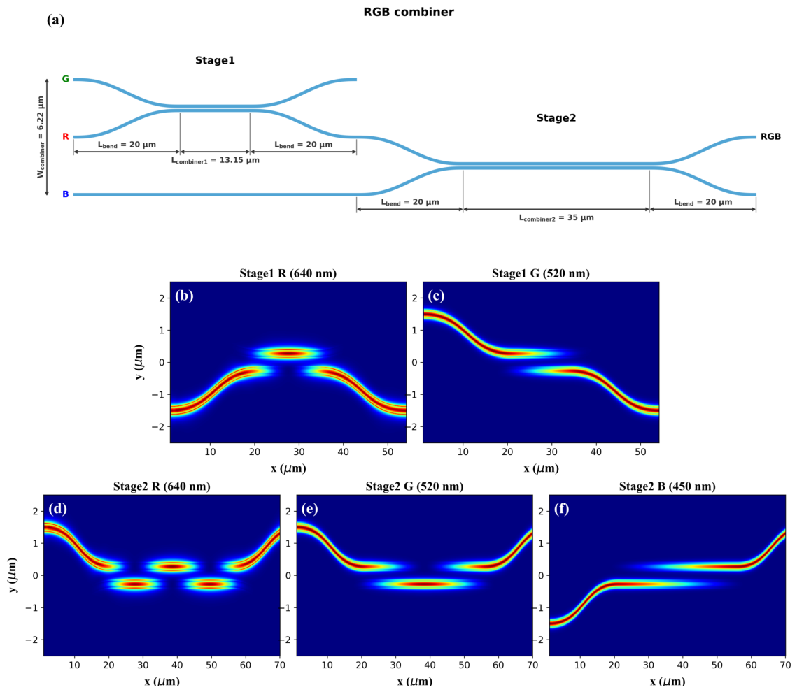
Further 3D FDTD simulations are carried out to optimize the structure, taking the input and output bends into consideration. Moreover, the red and green light combination stage is also simulated using the same , , and parameters. The introduction of the input and output bends will lead to a change in the length as the light coupling will also happen in the bend region. Thus, is optimised accordingly. The entire optimised RGB combiner structure is shown in Figure 6a. As discussed previously, the structure consists of two sequential coupling stages, denoted as stage 1 and stage 2. In stage 1, green light and red light are launched into the upper and lower input waveguides, respectively. The coupling section, with a length of , is designed to route both wavelengths into the lower output waveguide, which subsequently connects to the upper input of stage 2. Blue light is introduced through a separate straight waveguide connected to the lower input of stage 2. With a coupling length of , stage 2 is designed to combine the blue light with the red and green components at the output labeled RGB. Each coupling section is connected to input and output S-bends with a horizontal span of . The S-bends have a vertical span of 3 , resulting in a total structure width . Thus, the total structure has a footprint of 128.15 × 6.22 .
Figure 6.
(a) Schematic of the entire optimised RGB combiner structure. field evolution in the designed RGB combiner with input and output bends obtained using 3D FDTD simulations: (b) red light (640 nm) remains in the original waveguide at stage 1, (c) green light (520 nm) is coupled to the other waveguide at stage 1, (d) red light (640 nm) remains in the original waveguide at stage 2, (e) green light (520 nm) remains in the original waveguide at stage 2, and (f) blue light (450 nm) is coupled to the other waveguide at stage 2.
Owing to limited computational resources, the 3D FDTD simulations of stage 1 and stage 2 are carried out separately. The simulated three-dimensional evolution of the field in stage 1 is shown in Figure 6b,c. The red light and green light are both routed to the lower output waveguide. The simulated three-dimensional evolution of the field in stage 2 is shown in Figure 6d–f. Nearly all the red, green, and blue lights are combined in the same output waveguide. The red and green lights suffer from power loss in both stage 1 and stage 2, while the blue light only suffers from the power loss in stage 2. The total output powers for red, green, and blue light are 97.8%, 99.6%, and 99.9%, respectively, which remain high in the presence of the input and output S-bends. These values correspond to insertion losses, which is the power loss in dB, of 0.095, 0.019, and 0.004 dB for red, green, and blue light, respectively, including the power losses in both stage 1 and stage 2. However, we note here that it is possible to observe a slightly higher insertion loss due to the inter-stage transitions if the two stages are simulated in a single 3D FDTD simulation.
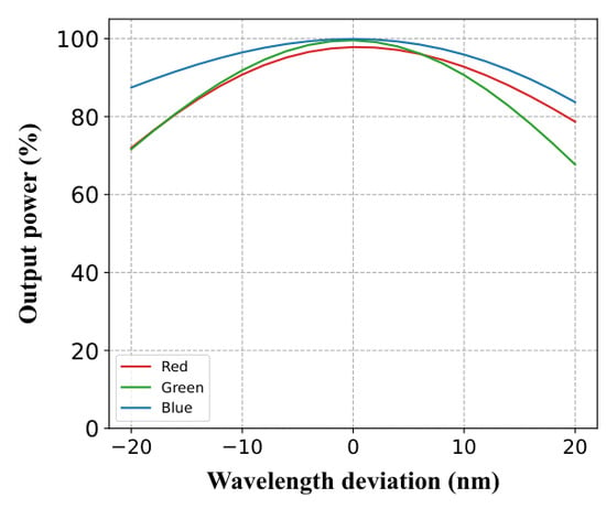
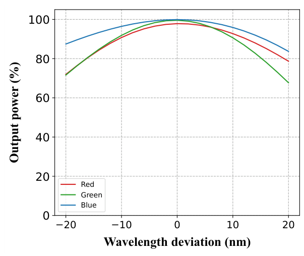
Additional simulations were performed to evaluate the wavelength sensitivity of the designed RGB combiner (with input/output bends), as shown in Figure 7. For wavelength deviations of up to nm from the nominal values, the output powers of the red, green, and blue channels remained above 90.8%, 90.6%, and 95.9%, respectively. These results correspond to insertion losses of 0.421 dB, 0.427 dB, and 0.182 dB for the red, green, and blue channels, respectively. These results demonstrate that the proposed combiner maintains high output power over a relatively broad wavelength range.
Figure 7.
Output power as a function of wavelength deviation for the red, green, and blue channels.
In HOE recording, a decrease in the red- and green-channel output powers to 90.8% and 90.6% at the largest wavelength deviations would shift the color balance (white point) of the recorded film, because the recorded diffraction gratings compete for the available refractive-index modulation [10]. However, the powers of the three input lasers are independently adjustable, so the white point can be restored by pre-adjusting the input powers, and this deviation therefore does not limit the practical operation of the combiner.
The emission linewidth of commercial RGB laser diodes is very narrow, so the laser linewidth itself does not limit the operation of the combiner. However, the wavelength-deviation results demonstrate the possibility of using lasers whose wavelengths deviate slightly from the nominal values, which simplifies source selection. In addition, the wavelength tolerance should be considered together with the fabrication tolerance: geometric deviations modify the effective-index difference and thereby shift the wavelengths at which the crossover-length condition holds, which acts on the device in the same way as a spectral detuning of the source. The fabrication-induced spectral detuning is expected to dominate and to limit the practical operation of the device rather than the linewidth of the laser. Thus, the above result shows its potential for a good fabrication tolerance. It should also be noted that the present study is currently at the simulation stage and the results obtained here are ideal. A real fabricated device would additionally suffer from various realistic losses, such as the waveguide propagation loss, bend loss (due to surface roughness of the bend, for example), etc., so its actual performance is expected to be somewhat worse than the simulated results reported above.
Table 4 summarizes representative integrated RGB combiners based on directional coupling and multimode or dual-mode interference. Silica planar lightwave circuit (PLC) directional couplers offer low insertion losses, although their longitudinal dimensions remain on the millimeter scale. Nakao et al. [16] reported simulated R/G/B insertion losses of for a device with a footprint of , while Sakamoto et al. [29] reduced the footprint to , with reported losses of . Interference-based designs provide alternative approaches to RGB combining. The SU-8 multimode interference (MMI) device presented by Sui et al. [30] achieved simulated losses at or below for all three channels, while retaining a millimeter-scale length. More compact silicon nitride (SiN) implementations include the dual-mode interference (DMI) device of Hu et al. [31] and the MMI device of Ali et al. [32], with footprints of and , respectively. These results illustrate the range of footprint and channel-loss characteristics achievable using different platforms and operating principles. The RGB combiner proposed in this work targets wavelengths of and occupies . Its simulated insertion losses of are lower than the corresponding values listed for the other devices, while its footprint is substantially smaller than those of the silica PLC and SU-8 implementations.
Table 4.
Comparison of representative integrated RGB combiners. Wavelengths and channel-specific insertion losses are listed in R/G/B order.
4. Discussion
The simulation results demonstrate that the proposed rib-waveguide RGB combiner provides efficient RGB beam combination while maintaining high tolerance to sidewall-angle deviations. According to the 3D FDTD and CMT results, the output power decrease is within 1.5% for red, green, and blue light when an sidewall-angle deviation is introduced in the fabrication. Moreover, rib waveguides have been reported to exhibit lower propagation loss than strip waveguides [33], suggesting that a rib-waveguide RGB combiner has the potential to exhibit low insertion loss. We note here again that this work remains an ideal numerical study, and a real fabricated device would possibly have a higher loss due to the presence of the taper, waveguide propagation loss, bend loss (due to surface roughness of the bend), etc.
Although this design is proposed for HOE film prototyping, the concept can also be applied to near-infrared wavelength-combining systems for optical communication and to the development of multichromatic optical engines. This work shows the possibility of reducing the sensitivity of a device to fabrication deviations by adjusting its design. This could help relax the fabrication requirements for such devices.
Author Contributions
Conceptualization, X.Z.; methodology, X.Z.; software, X.Z. and X.Y.; validation, X.Z. and X.Y.; formal analysis, X.Z.; writing—original draft preparation, X.Z.; writing—review and editing, X.Z., X.Y., H.L. and F.H.; visualization, X.Z.; supervision, H.L. and F.H.; project administration, H.L. and F.H. All authors have read and agreed to the published version of the manuscript.
Funding
This research was funded in part by the Guangdong Basic and Applied Basic Research Foundation, China, under Grant No. 2025A1515011508, and by the Shenzhen Science and Technology Program under Grant No. JCYJ20240813141606009.
Data Availability Statement
The data generated and/or analyzed during this study are available from the corresponding author upon reasonable request.
Acknowledgments
The authors gratefully acknowledge the Guangdong Provincial Key Laboratory of Laser Display Enterprise for a supportive research environment. We also thank the members of the laboratory for their technical assistance and helpful discussions.
Conflicts of Interest
Author Xin Zheng, Xudong Yan and Fei Hu was employed by the company Appotronics Co., Ltd. The remaining authors declare that the research was conducted in the absence of any commercial or financial relationships that could be construed as a potential conflict of interest.
Appendix A. Sensitivity to Additional Structural Parameters
Additional individual parameter sweeps are performed to evaluate the dimensional sensitivity of the rib- and strip-waveguide directional couplers (Designs 1 and 2). The investigated parameters are the waveguide width , gap width , total SiN thickness , and residual slab thickness . The nominal waveguide widths are 220 nm for the rib-waveguide design and 185 nm for the strip-waveguide design. Both designs have a nominal gap width of 320 nm and a total SiN thickness of 150 nm, while the rib-waveguide design has a residual slab thickness of 50 nm. Each parameter is varied individually from to nm relative to its nominal value in 5-nm increments, with the other geometric parameters held fixed. The TE-mode coupling efficiency at 520 nm is calculated using supermode analysis and coupled-mode theory as described previously.
As shown in Figure A1a, the rib-waveguide coupler exhibits lower sensitivity to waveguide-width deviations than the strip-waveguide coupler. Over the sampled nm range, the minimum transmittances are 87.22% and 70.64% for the rib- and strip-waveguide designs, respectively. The rib-waveguide design also exhibits higher transmittance at all sampled nonzero gap-width deviations (Figure A1b), with a minimum of 94.14%, compared with 92.25% for the strip-waveguide design. These results indicate improved tolerance to the investigated lateral dimensional deviations.
The two designs exhibit similar sensitivity to total SiN thickness deviations, as shown in Figure A1c. The minimum sampled transmittances are 91.79% for the rib-waveguide design and 92.53% for the strip-waveguide design, with the strip-waveguide design performing slightly better at all sampled nonzero deviations. The residual slab thickness introduces an additional sensitivity for the rib-waveguide coupler (Figure A1d): the transmittance decreases to 89.92% and 86.24% at slab-thickness deviations of and nm, respectively. Thus, improved lateral dimensional tolerance does not eliminate the need for thickness and etch-depth control.
For the sampled deviations within nm, the minimum transmittances of the rib-waveguide design are 97.02%, 98.62%, 98.14%, and 96.48% for variations in waveguide width, gap width, total SiN thickness, and residual slab thickness, respectively. The thickness sweeps isolate geometric sensitivities: is fixed during the sweep, whereas is fixed during the sweep. We note here that the investigated ranges are deterministic test conditions rather than measured process distributions. These single-wavelength sweeps quantify individual parameter sensitivities; they do not provide a statistical yield prediction or an assessment of simultaneous dimensional variations in the complete RGB combiner.
Figure A1.
Sensitivity of the calculated TE-mode transmittance at 520 nm to deviations in (a) waveguide width , (b) gap width , (c) total SiN thickness , and (d) residual slab thickness . Red solid lines and blue dashed lines denote the rib- and strip-waveguide directional couplers, respectively. Only the rib-waveguide design is included in (d), as the strip waveguide has no residual slab. Deviations are measured relative to the nominal dimensions. Each parameter is varied individually, with the other geometric parameters and the physical interaction length held fixed.
Appendix B. Single-Mode Condition Verification
Modal effective-index calculation is carried out using the MODE solver. For the isolated 220-nm-wide rib waveguide of Design 3, the calculation shows that only TE and TM fundamental modes are supported at 450, 520, and 640 nm. The corresponding effective indices are shown in Table A1 and the mode profiles are shown in Figure A2. The higher-order TE and TM modes are below cutoff at all three wavelengths and are no longer guided in the rib region.
Figure A2.
Calculated mode profiles of TE and TM fundamental modes at (a) 450 nm, (b) 520 nm, and (c) 640 nm.
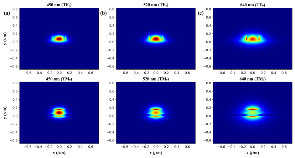
Table A1.
Modal effective indices of TE and TM fundamental modes at 450, 520, and 640 nm.
Appendix C. FDTD Simulation Setup
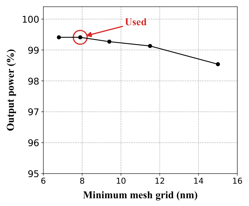
An automatic nonuniform mesh is used for the FDTD simulation. A numerical convergence analysis is done at 450 nm. The transmission value converges with respect to mesh resolution, as shown in Figure A3. Thus, a minimum mesh size of 7.9 nm is chosen to provide good simulation accuracy and a reasonable simulation time. PML boundary conditions are used, and the total PML thickness is around 260 nm for simulations at 450 nm. The simulation time is set to 3000 fs, which is long enough for light propagation. The output power recorded by the monitor is normalized by the input source power. The refractive index of SiN is fixed at 2.03 and the refractive index of SiO2 is based on the Palik database, which is available in Lumerical.
Figure A3.
The output power as a function of the mesh grid size for Design 3 at 450 nm. The transmission value converges with respect to mesh resolution.
References
- Xiong, J.; Hsiang, E.L.; He, Z.; Zhan, T.; Wu, S.T. Augmented reality and virtual reality displays: Emerging technologies and future perspectives. Light. Sci. Appl. 2021, 10, 216. [Google Scholar] [CrossRef] [Scilit]
- Zhan, T.; Yin, K.; Xiong, J.; He, Z.; Wu, S.T. Augmented reality and virtual reality displays: Perspectives and challenges. Iscience 2020, 23, 101397. [Google Scholar] [CrossRef] [Scilit]
- Liu, Z.; Wang, D.; Gao, H.; Li, M.; Zhou, H.; Zhang, C. Metasurface-enabled augmented reality display: A review. Adv. Photonics 2023, 5, 034001. [Google Scholar] [CrossRef] [Scilit]
- Shi, Z.; Cheng, R.; Wei, G.; Hickman, S.A.; Shin, M.C.; Topalian, P.; Wang, L.; Coso, D.; Wang, Y.; Wang, Q.; et al. Flat-panel laser displays through large-scale photonic integrated circuits. Nature 2025, 644, 652–659. [Google Scholar] [CrossRef] [Scilit]
- Jang, C.; Mercier, O.; Bang, K.; Li, G.; Zhao, Y.; Lanman, D. Design and fabrication of freeform holographic optical elements. ACM Trans. Graph. (TOG) 2020, 39, 1–15. [Google Scholar] [CrossRef] [Scilit]
- Yan, X.; Zhu, J.; Liu, M.; Liu, Y.; Luo, D. Colorful multi-plane augmented reality display with dynamically tunable reflective Pancharatnam-Berry phase lens. Opt. Express 2024, 32, 9161–9170. [Google Scholar] [CrossRef] [Scilit]
- Chakraborty, D.; Georgiev, R.; Aspell, S.; Toal, V.; Naydenova, I.; Cody, D.; Martin, S. Modelling and design of holographic optical elements for beam-coupling applications for a range of incident beam angles. Photonics 2022, 9, 936. [Google Scholar] [CrossRef] [Scilit]
- Wakunami, K.; Hsieh, P.Y.; Oi, R.; Senoh, T.; Sasaki, H.; Ichihashi, Y.; Okui, M.; Huang, Y.P.; Yamamoto, K. Projection-type see-through holographic three-dimensional display. Nat. Commun. 2016, 7, 12954. [Google Scholar] [CrossRef] [Scilit]
- Xu, H.; Xu, Y.; Wang, C.; Liu, J. Curved holographic augmented reality near-eye display system based on freeform holographic optical element with extended field of view. Photonics 2024, 11, 1194. [Google Scholar] [CrossRef] [Scilit]
- Wilm, T.; Kibgies, J.; Fiess, R.; Stork, W. Multiplexed holographic combiner with extended eye box fabricated by wave front printing. Photonics 2022, 9, 419. [Google Scholar] [CrossRef] [Scilit]
- Lee, J.S.; Kim, Y.K.; Won, Y.H. See-through display combined with holographic display and Maxwellian display using switchable holographic optical element based on liquid lens. Opt. Express 2018, 26, 19341–19355. [Google Scholar] [CrossRef] [Scilit]
- Bruder, F.K.; Fäcke, T.; Grote, F.; Hagen, R.; Hönel, D.; Koch, E.; Rewitz, C.; Walze, G.; Wewer, B. Mass production of volume holographic optical elements (vHOEs) using Bayfol (R) HX photopolymer film in a roll-to-roll copy process. In Proceedings of the Practical Holography XXXI: Materials and Applications; SPIE: Bellingham, WA, USA, 2017; Volume 10127, pp. 63–82. [Google Scholar]
- Lee, S.; Jang, C.; Moon, S.; Cho, J.; Lee, B. Additive light field displays: Realization of augmented reality with holographic optical elements. ACM Trans. Graph. (TOG) 2016, 35, 1–13. [Google Scholar]
- Bruder, F.K.; Fäcke, T.; Hagen, R.; Hönel, D.; Kleinschmidt, T.P.; Orselli, E.; Rewitz, C.; Rölle, T.; Walze, G. Diffractive optics in large sizes: Computer-generated holograms (CGH) based on Bayfol HX photopolymer. In Proceedings of the Advances in Display Technologies V; SPIE: Bellingham, WA, USA, 2015; Volume 9385, pp. 40–53. [Google Scholar]
- Nakao, A.; Yamada, S.; Katsuyama, T.; Kawasaki, O.; Iwabata, K.; Yabe, Y.; Horii, K.; Himeno, A. Compact full-color laser beam scanning image projector based on a waveguide-type RGB combiner. J. Soc. Inf. Disp. 2022, 30, 24–32. [Google Scholar] [CrossRef] [Scilit]
- Nakao, A.; Morimoto, R.; Kato, Y.; Kakinoki, Y.; Ogawa, K.; Katsuyama, T. Integrated waveguide-type red-green-blue beam combiners for compact projection-type displays. Opt. Commun. 2014, 330, 45–48. [Google Scholar] [CrossRef] [Scilit]
- Mashayekh, A.T.; Klos, T.; Geuzebroek, D.; Klein, E.; Veenstra, T.; Büscher, M.; Merget, F.; Leisching, P.; Witzens, J. Silicon nitride PIC-based multi-color laser engines for life science applications. Opt. Express 2021, 29, 8635–8653. [Google Scholar] [CrossRef] [Scilit]
- Roeloffzen, C.G.; Hoekman, M.; Klein, E.J.; Wevers, L.S.; Timens, R.B.; Marchenko, D.; Geskus, D.; Dekker, R.; Alippi, A.; Grootjans, R.; et al. Low-loss Si3N4 TriPleX optical waveguides: Technology and applications overview. IEEE J. Sel. Top. Quantum Electron. 2018, 24, 4400321. [Google Scholar] [CrossRef] [Scilit]
- Smith, J.A.; Francis, H.; Navickaite, G.; Strain, M.J. SiN foundry platform for high performance visible light integrated photonics. Opt. Mater. Express 2023, 13, 458–468. [Google Scholar] [CrossRef] [Scilit]
- Buzaverov, K.A.; Baburin, A.S.; Sergeev, E.V.; Avdeev, S.S.; Lotkov, E.S.; Andronik, M.; Stukalova, V.E.; Baklykov, D.A.; Dyakonov, I.V.; Skryabin, N.N.; et al. Low-loss silicon nitride photonic ICs for near-infrared wavelength bandwidth. Opt. Express 2023, 31, 16227–16242. [Google Scholar] [CrossRef] [Scilit]
- Chavez Boggio, J.; Bodenmüller, D.; Fremberg, T.; Haynes, R.; Roth, M.; Eisermann, R.; Lisker, M.; Zimmermann, L.; Böhm, M. Dispersion engineered silicon nitride waveguides by geometrical and refractive-index optimization. J. Opt. Soc. Am. B 2014, 31, 2846–2857. [Google Scholar] [CrossRef] [Scilit]
- Chrostowski, L.; Hochberg, M. Silicon Photonics Design: From Devices to Systems, 1st ed.; Cambridge University Press: Cambridge, UK, 2015. [Google Scholar]
- Ansys Lumerical, MODE: Waveguide Simulator. Available online: https://www.ansys.com/products/optics/mode (accessed on 25 October 2026).
- Yariv, A. Coupled-mode theory for guided-wave optics. IEEE J. Quantum Electron. 1973, 9, 919–933. [Google Scholar] [CrossRef] [Scilit]
- Yariv, A.; Yeh, P. Photonics: Optical Electronics in Modern Communications, 6th ed.; Oxford University Press: New York, NY, USA, 2006. [Google Scholar]
- Singh, N.; Lorenzen, J.; Wang, K.; Gaafar, M.A.; Sinobad, M.; Francis, H.; Edelmann, M.; Geiselmann, M.; Herr, T.; Garcia-Blanco, S.M.; et al. Watt-class silicon photonics-based optical high-power amplifier. Nat. Photonics 2025, 19, 307–314. [Google Scholar] [CrossRef] [Scilit]
- Ji, X.; Ning Wang, R.; Liu, Y.; Riemensberger, J.; Qiu, Z.; Kippenberg, T.J. Efficient mass manufacturing of high-density, ultra-low-loss Si3N4 photonic integrated circuits. Optica 2024, 11, 1397–1407. [Google Scholar] [CrossRef] [Scilit]
- Ansys Lumerical, FDTD: 3D Electromagnetic Simulator. Available online: https://www.ansys.com/products/optics/fdtd (accessed on 25 October 2026).
- Sakamoto, J.; Goh, T.; Katayose, S.; Watanabe, K.; Itoh, M.; Hashimoto, T. Compact and low-loss RGB coupler using mode-conversion waveguides. Opt. Commun. 2018, 420, 46–51. [Google Scholar] [CrossRef] [Scilit]
- Sui, G.; Liu, F.; Guo, H.; Chen, Z. Flexible broadband white light multimode interference coupler. Opt. Express 2021, 29, 29730–29744. [Google Scholar] [CrossRef] [Scilit]
- Hu, X.L.; Jiang, J.K.; Liu, W.J. Low-loss and broadband cascaded SiN RGB coupler with dual-mode interference. Appl. Opt. 2023, 62, 944–949. [Google Scholar] [CrossRef] [Scilit]
- Ali, F.; Figeys, B.; Shramkova, O.; Jansen, R.; Rottenberg, X.; Gehlhaar, R.; Genoe, J. Ultracompact RGB (de) multiplexer based on a silicon nitride dual-segmented MMI. Opt. Lett. 2026, 51, 3749–3752. [Google Scholar] [CrossRef] [Scilit]
- Lindecrantz, S.M.; Hellesø, O.G. Estimation of propagation losses for narrow strip and rib waveguides. IEEE Photonics Technol. Lett. 2014, 26, 1836–1839. [Google Scholar] [CrossRef] [Scilit]

Disclaimer/Publisher’s Note: The statements, opinions and data contained in all publications are solely those of the individual author(s) and contributor(s) and not of MDPI and/or the editor(s). MDPI and/or the editor(s) disclaim responsibility for any injury to people or property resulting from any ideas, methods, instructions or products referred to in the content. |
© 2026 by the authors. Licensee MDPI, Basel, Switzerland. This article is an open access article distributed under the terms and conditions of the Creative Commons Attribution (CC BY) license.