


Abstract
InGaAs photocathodes operating in the 0.9–1.7 μm spectral band are fundamentally limited by optical reflection losses and incomplete light absorption in thin active layers. In this work, we constructed periodic micro-nanostructured InGaAs photocathode models using finite-difference time-domain (FDTD) simulations, and systematically compared five micro-nanostructures (square pillars, circular pillars, square truncated pyramids, hexagonal prisms, and square pyramids) against a planar reference structure. At a wavelength of 1.55 μm, coupled scans of lateral dimension and height yielded maximum absorptance values of 0.749 for square pillars (0.6 μm side length, 0.9 μm height) and 0.682 for circular pillars (0.9 μm diameter, 0.9 μm height), corresponding to enhancements of 35.4% and 23.3%, respectively, relative to the planar reference. Circular pillars exhibited the lowest reflectance (0.072); however, their higher forward transmittance caused lower overall absorptance than that of square pillars. We then coupled the FDTD generation profiles to a steady-state drift-diffusion analysis of carrier collection. Under normalized illumination and a 5 V bias, the integrated generation increased by 29.2%. The modeled internal generation-rate-weighted collection efficiency ηC increased from 0.499 to 0.680, corresponding to a 36.2% enhancement, and the internally collected carrier-rate proxy increased by 76.1% relative to the planar reference. Under ideal fully-passivated side-wall conditions, the internally collected carrier-rate proxy increased by 76.1% relative to the planar reference. This study provides theoretical guidance for designing and optimizing high-performance micro/nanostructured InGaAs photocathodes.
1. Introduction
InGaAs-based heterostructure semiconductors exhibit excellent spectral response and photoelectric conversion performance in the 1.0–1.7 μm short-wave infrared (SWIR) band. Consequently, they are widely used as absorption layers in optical-fiber communication, lidar, three-dimensional low-light imaging, and single-photon-detection systems [1,2,3,4]. In a transmission-mode InGaAs photocathode, photons enter through the window side and generate carriers in the InGaAs absorption layer; the carriers then diffuse toward the emission surface and are emitted into vacuum, producing the photocurrent. Because light incidence and photoelectron emission occur on opposite sides of the device, this architecture can be integrated with optical focusing systems and microchannel plates, making it valuable for low-light and weak-signal imaging applications [5,6,7]. Photon absorption directly affects the quantum efficiency, the signal-to-noise ratio, and ultimate detection sensitivity; it is therefore a fundamental performance bottleneck in SWIR detection.
Conventional planar thin-film InGaAs photocathodes conventionally increase photon absorptance by increasing the thickness of the absorption layer. However, this strategy also lengthens the carrier-transport path, thereby exacerbating bulk-recombination losses. Conversely, reducing the absorption-layer thickness mitigates transport-related losses but substantially compromises SWIR absorptance [8]. Existing approaches either tune the InGaAs composition and doping profile to improve carrier transport or deposit antireflection coatings to reduce Fresnel reflection. Neither approach alone removes the optical absorption limit of a planar thin film; achieving both high absorptance and low transport loss therefore remains challenging.
Micro-nanostructure light-field engineering offers a promising way to address this trade-off. Integrating periodic micro-nanostructures into the active layer can reshape electromagnetic-wave propagation and the spatial distribution of optical energy without increasing the total device thickness. Through a graded effective refractive index, optical-path folding, near-field localization, and high-index dielectric resonances, such arrays can improve photon utilization within ultrathin absorption layers. Brongersma et al. demonstrated that high-index nanostructures can substantially improve light trapping in thin-film photovoltaics through scattering, optical-path folding, and near-field localization [9]. Kuznetsov et al. summarized the electromagnetic design rules for dielectric nanoresonators, identifying geometry and characteristic size as key determinants of resonance modes and near-field distributions [10]. Van de Groep and Polman further clarified the roles of the substrate environment and resonator height in the resonance phase and modal coupling [11]. The same light-management strategy has improved infrared absorption in photovoltaic and silicon-detector platforms, including nanopillars, metasurface gratings, and relief-cone structures [12,13,14].
Recently, micro-nanostructures have been actively explored for transmission-mode negative-electron-affinity photocathodes, particularly in GaAs-based near-infrared systems. Peng et al. fabricated an all-dielectric metasurface on the window layer of ultrathin GaAs photocathodes, achieving wavelength-selective quantum efficiency enhancement together with a reduced temporal response [15]. Li et al. designed arrays of nanocircular pillars on an AlGaAs incident window layer and reported a 1.4-fold increase in average quantum efficiency across 700–920 nm through Mie-resonance-induced near-field localization, while preserving compatibility with inverted-structure fabrication [16]. However, studies of InGaAs SWIR detectors remain less systematic: Zhang et al. examined incident-side photon-trapping microstructures for InGaAs/Si avalanche photodiodes [17], whereas Dong et al. investigated dielectric-metasurface-enhanced absorption in silicon-based InGaAs detectors [18]. To date, no comprehensive systematic study has addressed light trapping in transmission-mode InGaAs photocathodes.
To bridge this gap, this work establishes FDTD models of micro-nanostructures with multiple morphologies and geometric parameters on the photon-incident side of the InGaAs absorption layer in transmission-mode photocathodes. Planar films, square pillars, circular pillars, hexagonal prisms, square truncated pyramids, and square pyramids were compared in terms of absorptance and reflectance, while cross-sectional electric-field distributions and classical electromagnetic theory were used to identify the physical origin of the optical response. Univariate scans of lateral size and pillar height, followed by two-dimensional coupled scans, were used to determine resonance-matching windows and their cross-parameter interactions. Crucially, because optical absorptance alone does not establish a carrier-collection benefit of a structure, the optical generation profile was subsequently coupled to a drift-diffusion transport calculation. The resulting integrated optoelectronic framework provides both fundamental physical insight and quantitative design guidelines for high-performance SWIR InGaAs photocathodes incorporating micro- and nanostructured light-trapping architectures.
2. Structures and Methods
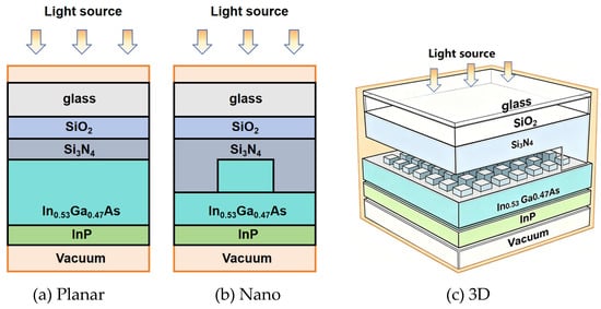
As shown in Figure 1, the three-dimensional model of the transmission-mode InGaAs photocathode is stacked along the optical-propagation z-axis. The normally incident photons enter from the window-glass side and successively pass through window glass, a 0.2 μm SiO2 buffer layer, a 0.2 μm Si3N4 antireflection layer, a 1 μm In0.53Ga0.47As absorption layer, and a 0.1 μm InP electron-emission layer. The planar and micro-nanostructured models have identical material stacks and total layer thicknesses. In the structured models, features up to 0.9 μm high were patterned on the photon-incident side of the In0.53Ga0.47As layer. The incident direction is from the glass side toward the InP emission side; this orientation is used consistently in all field maps.
Figure 1.
Simulated unit cells of (a) the planar and (b) the micro-nanostructured InGaAs photocathodes; (c) three-dimensional view of the micro-nanostructured photocathode.
Five common periodic InGaAs micro-nanostructures comprising square pillars, circular pillars, hexagonal prisms, square truncated pyramids, and square pyramids were evaluated against a planar thin-film reference. All arrays were arranged in square unit cells with a fixed period of 1 μm. Unless otherwise stated, the lateral characteristic size and height were both 0.5 μm. The top side length of the square truncated pyramid was 0.3 μm, and the square pyramid tapered symmetrically to an apex. For height scans, each increase in protruding feature height was balanced by an equal reduction in the underlying planar InGaAs thickness, keeping the overall InGaAs layer envelope at 1 μm. Because equal nominal dimensions do not produce equal fill factors or absorber volumes, Table 1 reports the fill factor, normalized InGaAs volume VInGaAs, and volume-normalized absorptance index A/VInGaAs. These quantities separate, as far as possible, morphology-dependent optical effects from differences in absorber inventory; complete decoupling would require additional equal-fill-factor and/or equal-volume simulations.
Table 1.
Geometry audit for the fixed-size morphology sweep. VInGaAs is normalized to the planar unit-cell volume; VInGaAs is a volume-normalized absorptance index at 1.55 μm.
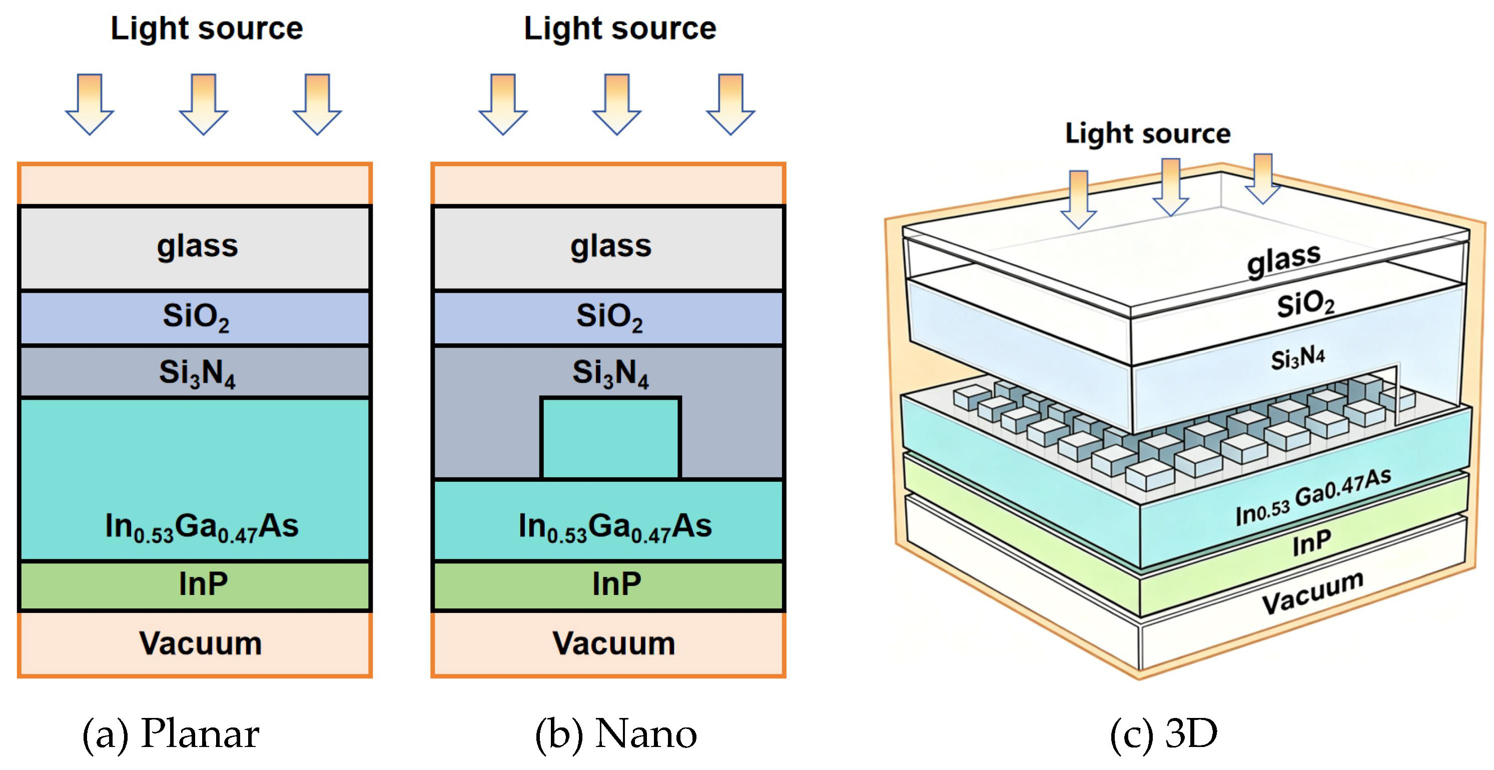
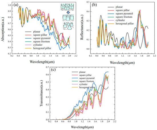
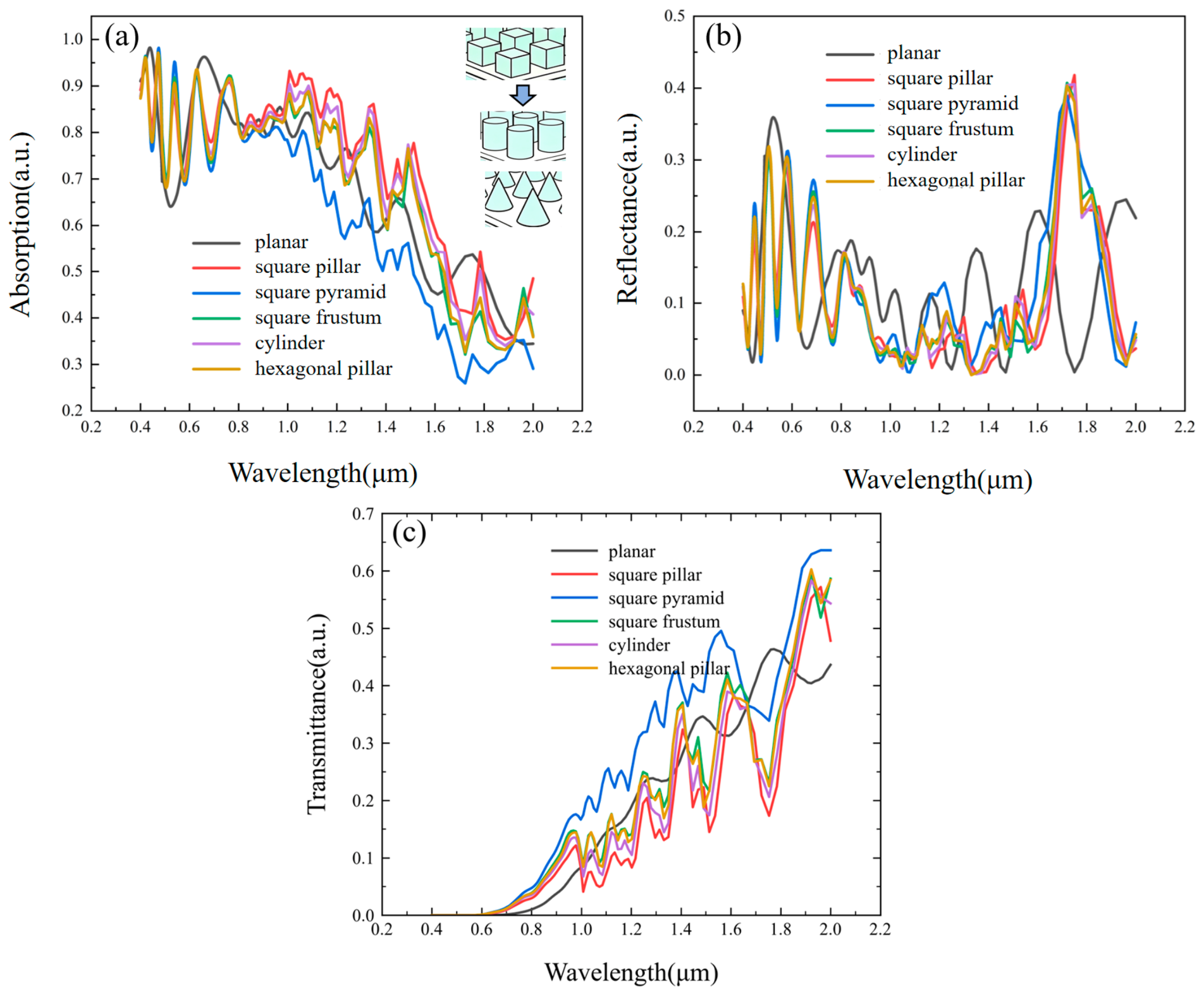
The optical response was calculated by solving the full-vector Maxwell equations using the FDTD method. The simulation workflow included model construction, material assignment, boundary-condition setting, mesh-convergence verification, source excitation, field monitoring, time-domain iteration, and frequency-domain post-processing. The refractive indices of SiO2, Si3N4, and InP were obtained from Palik’s Handbook of Optical Constants of Solids [19], whereas the refractive index and extinction coefficient of In0.53Ga0.47As were obtained from established spectroscopic-ellipsometry measurements. A normally incident plane wave spanned 0.4–2 μm. Transmission and reflection monitors were placed at the exit and incident sides, respectively, to obtain broadband transmittance and reflectance. The transmittance spectrum is reported together with absorptance and reflectance in Figure 2, and is used explicitly when discussing leakage. A central cross-sectional field monitor recorded the electric-field amplitude distribution used for mechanism analysis.
Figure 2.
Absorptance (a), reflectance (b), and transmittance (c) spectra of structures with different morphologies.
Mesh convergence was verified before the parameter studies, with local refinement in the micro-nanostructures region. The final nonuniform mesh had a maximum global step of 0.05 μm and a local step of 0.02 μm in the structured region. The convergence criterion was a relative change in absorptance at 1.55 μm below 0.1%, which ensures that the reported spectral trends were insensitive to further mesh refinement.
Post-processing and quantitative analysis followed classical electromagnetic-optics theory and energy conservation. For time-harmonic fields in a nonmagnetic, linear, isotropic dielectric, incident energy is partitioned into reflected, transmitted, and absorbed components. The normalized spectral absorptance was obtained from the reflectance and transmittance:
where A(λ), R(λ), and T(λ) are the normalized absorptance, reflectance, and transmittance at wavelength λ, respectively. The relationship between the microscopic field and absorption loss follows from the frequency-domain Poynting theorem. The time-averaged volumetric absorption power density characterizes the local photon-dissipation rate, and is the standard FDTD loss expression [11]:
where ω is the angular frequency, ε0 is the vacuum permittivity, ε″(r,ω) is the imaginary part of the relative permittivity, and |E(r,ω)| is the magnitude of the local electric field at position r. The total effective absorbed power is obtained by integrating the time-averaged volumetric absorption power density over the absorption region, as follows:
Device-level absorptance is determined by the total spatial overlap integral between the high-field regions and the absorbing medium, rather than the single-point peak electric field intensity. To complete the theoretical framework for the mechanism analysis, effective medium theory and Fabry–Pérot resonance theory are introduced to assist interpretation. The modulation effect of the microstructure fill factor on interfacial reflectance was quantified using the in-plane equivalent-refractive-index formula [20], and the resonance-matching mechanism of the structural dimensions was explained using the longitudinal phase-closure condition [21]. These models provide a physically constrained interpretation of the simulation data; they do not replace the FDTD results.
Optical absorption enhancement does not by itself demonstrate improved carrier collection. Therefore, a steady-state drift-diffusion carrier-collection calculation was coupled with the FDTD results using the CHARGE solver, an optical-electrical workflow widely used to connect spatial photogeneration with carrier transport in photodiodes and photodetectors. At 1.55 μm, the local optical generation rate was calculated from the FDTD absorption power density as follows:
where is the reduced Planck constant. The electric field was recorded throughout the 1 μm × 1 μm unit cell. The resulting three-dimensional generation profile was averaged in the transverse direction and imported into the two-dimensional transport model.
The collection probability CP(x) is the probability that a photoelectron generated at depth x successfully reaches the semiconductor emission interface, accounting for bulk recombination and surface-recombination losses during transport toward the modeled collection boundary. Sidewall recombination is not explicitly resolved after transverse averaging and is treated separately as a sensitivity bound, in Section 3.5. This quantity describes only internal semiconductor carrier-transport losses, and does not include the escape process by which photoelectrons cross the surface barrier into vacuum. For one-dimensional planar photocathodes, CP(x) can be expressed using hyperbolic analytical solutions. However, the micro-nanostructure array in this work introduces three-dimensional geometric boundaries, so no simple elementary analytical formula is available; discrete CP(x) values are therefore obtained by numerical drift-diffusion solving. The product of the local generation rate G(x) and collection probability CP(x) gives the effective internally collected-carrier supply at that depth.
The generation-rate-weighted average collection efficiency ηC quantifies the overall carrier-collection capability within the absorber layer, and is given by
In this expression, G(x) is the depth-dependent photoelectron-generation rate and CP(x) is the depth-resolved collection probability.
Optical absorption alone does not establish photocathode emission. Accordingly, the electrical simulations presented here constitute a carrier-collection analysis, rather than a complete photocathode-emission model. The planar and square-pillar structures were evaluated under matched electrical and numerical conditions, with a steady-state bias of 5 V applied between the InP-side contact and the opposing contact. Both illuminated and dark calculations were performed for each structure. Except for the in-plane geometry and the corresponding geometry-matched FDTD generation profile, all other simulation inputs were kept unchanged, including the material parameters, nominal doping types and concentrations, SRH lifetimes, Auger and radiative recombination coefficients, contact definitions, applied bias, illumination normalization, wavelength, mesh settings, and solver tolerances. Thus, the geometry and its associated FDTD generation profile are intentionally different between the two structures, whereas all other electrical and numerical parameters remain identical. This contact-based drift-diffusion formulation is standard for semiconductor photodetectors [22,23]. The model solves the electrostatic potential and carrier transport, while accounting for optical generation and Shockley–Read–Hall (SRH), Auger, and radiative recombination. The reported CHARGE outputs include the electron and hole concentrations (n and p), electron and hole current densities (Jn and Jp), external optical-generation rate (Gop,ext), individual recombination components, and the carrier-collection efficiency ηC, which is derived from carrier transfer to the modeled collection boundary. Here, ηC denotes the fraction of generated carriers delivered to that boundary under the specified bias, and does not represent emission into vacuum. Because the CHARGE model does not include negative-electron-affinity (NEA) emission, vacuum transport, or electron escape, ηC and the collected-electron-rate proxy are internal semiconductor quantities and should be interpreted as upper bounds for a subsequent emission analysis. They must therefore not be reported as internal or external quantum efficiency (IQE or EQE) without an explicit NEA-emission and escape model.
The transport calculation uses a two-dimensional x-z drift-diffusion model and imports the unit-cell-averaged optical-generation rate. This transverse averaging procedure eliminates the geometric information of pillar sidewall perimeters; therefore, sidewall surface-recombination boundaries and surface-recombination velocity (SRV) are not directly incorporated into the drift-diffusion solver. All carrier-collection metrics including ηC and internally collected carrier-rate proxy are simulated under the idealized fully-passivated sidewall assumption with zero sidewall recombination, which serves as an upper bound for practical devices. The electrical comparison therefore represents an idealized, effectively passivated-sidewall limit, and is intended only to compare relative generation and collection under matched conditions; it is not an absolute device efficiency. Using As/VInGaAs = 3.46 μm−1, a first-order surface-loss estimate scales as S·As/VInGaAs: the passivated value S = 260 cm s−1 corresponds to a volumetric loss rate of approximately 9.0 × 10⁶ s−1, whereas the unpassivated value S = 2.2 × 104 cm s−1 corresponds to approximately 7.6 × 10⁸ s−1. For reference, the effective bulk recombination rate in the baseline planar structure is in the order of 107 s−1. Thus, the passivated sidewall loss is comparable to the effective bulk loss scale and cannot be assumed to be negligible, while the unpassivated sidewall loss dominates and would substantially suppress carrier-collection efficiency. The SRV values used here are adopted as literature-based sensitivity endpoints. Reference [24] provides the directly relevant InGaAs/InP nanopillar passivation context, whereas the additional passivation reference is used only as general background and is not treated as a direct measurement of the present structure.
3. Results and Analysis
3.1. Effect of Micro-Nanostructure Morphology on Absorptance
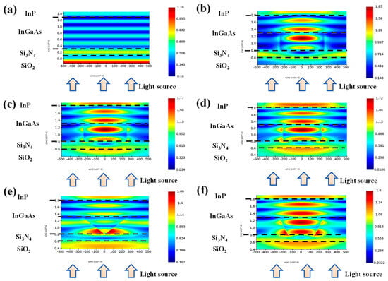
With the total InGaAs thickness fixed, the absorptance and reflectance of the five micro-nanostructure morphologies and the planar reference were compared over 0.4–2 μm. The resulting spectra show that morphology strongly governs both the magnitude and spectral character of light trapping, as shown in Figure 3.
Figure 3.
Cross-sectional electric-field distributions for (a) the planar, (b) square-pillar, (c) circular-pillar, (d) hexagonal-prism, (e) square-pyramid, and (f) square-truncated-pyramid structures. Color bars are panel-specific, and are not intended for direct quantitative comparison.
The initial morphology sweep fixed the nominal lateral size and height, so the fill factor and InGaAs volume were not identical across shapes. For a 1 μm period, a 0.5 μm feature height, and the 0.3 μm top width used for the square truncated pyramids, the geometric audit gives the values in Table 1. The fill factor spans 0.083–0.250 and the normalized InGaAs volume spans 0.542–0.625 for the patterned structures. The volume-normalized absorptance index A/VInGaAs retains the square-pillar advantage, but it also shows that the raw absorptance differences include contributions from both fill factor and absorber volume. Thus, this fixed-size sweep does not fully isolate morphology; equal-fill-factor and/or equal-volume simulations would be required for a strictly morphology-only comparison.
It should be emphasized that the above absorptance comparison is performed under fixed feature dimensions, rather than fixed fill factor or fixed InGaAs absorber volume. As summarized in Table 1, different nanostructure morphologies yield distinct fill factors and normalized InGaAs volumes. The higher raw absorptance of the square-pillar array originates from the combined contributions of the dielectric-resonance light-trapping effect and larger absorber material volume. The volume-normalized absorptance index A/VInGaAs partially eliminates the volume difference, and still retains the advantage of square pillars. Nevertheless, this index cannot completely decouple morphological resonance effect from fill-factor-induced optical modulation. Strict quantitative comparison purely for morphology effect requires additional control-variable simulations with identical fill factor or equal absorber volume, which is beyond the scope of the present work and will be considered in follow-up research. Interfacial reflectance is not simply positively correlated with absorptance. Circular pillars provide the smoothest graded transition in effective refractive index because their curved sidewalls produce a continuously varying cross-sectional fill factor: for a circular pillar of radius r in a unit cell of period P, the transverse filling profile is f(x) = 2√(r2 − x2)/P within the pillar, and vanishes continuously at the sidewall; thus, the area-averaged effective index obtained from the effective-medium relation in [20] also changes smoothly. A square pillar, in contrast, changes abruptly from air to InGaAs at a vertical sidewall. This geometric continuity weakens the local Fresnel discontinuity, consistent with the lowest interfacial reflectance of 0.072 at 1.55 μm. However, circular pillars exhibit greater forward-transmittance leakage: a larger fraction of incident photons passes through the absorption layer and leaves the device, so the low-reflectance benefit is not fully converted into absorptance. Although square pillars have slightly higher interfacial reflectance than circular pillars, they support stronger dielectric-resonance confinement and reduce transmittance leakage, yielding the highest absorptance in this fixed-size comparison. The remaining morphologies exhibit the same trade-off among reflectance, transmittance, resonance confinement, and absorber volume.
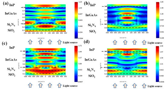
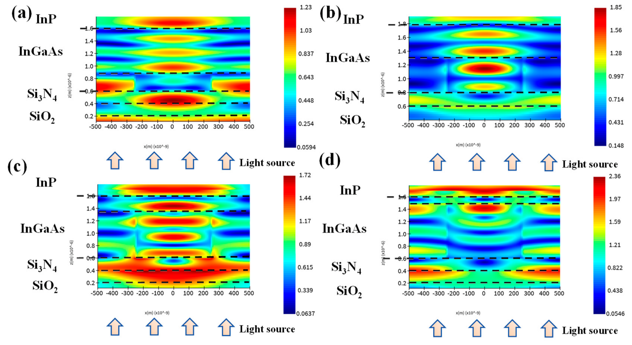
The time-averaged volumetric absorption power density is proportional to |E|2, and the total absorbed power is determined by the spatial volume integral of field energy within the InGaAs layer. Therefore, the field analysis focuses not only on peak field intensity, but also on whether high-field regions are confined within the absorber, on their spatial coverage, and on their overlap with the effective absorption volume. As clarified in each figure caption, the color scales of these field plots are panel-specific. They only serve to illustrate the spatial distribution of high-field regions within each individual structure, and direct visual comparison of color intensity across different structures is not quantitatively valid. Performance comparisons between structures are based exclusively on integrated spectral metrics and volume-integrated absorption power density.
The three straight-columnar structures—square pillars, circular pillars, and hexagonal prisms—introduce lateral refractive-index modulation, excite Mie-type dielectric resonances, and confine enhanced fields in the absorption layer. Square pillars provide the largest overlap between high-field regions and InGaAs and the broadest transverse coverage, combining low transmittance loss with the highest absorptance. Circular pillars yield a smoother interfacial transition and lower reflectance, but their weaker confinement and poorer field-volume overlap increase transmittance leakage. Hexagonal prisms lie between these two cases. The field distributions for square pyramids and square truncated pyramids confirm that low reflectance is not equivalent to high absorptance: their graded profiles reduce the index step, but insufficient resonance confinement and poor overlap with the InGaAs volume leave substantial transmittance leakage. Morphology selection therefore depends on the field-energy volume integral in the absorber, with dielectric resonance, effective refractive index, and fill factor acting together.
Columnar structures (square pillars, circular pillars, and hexagonal prisms) exhibit higher absorptance than pyramidal structures overall because of their stronger resonance confinement. Among them, square and circular pillars achieve the highest and second-highest absorptance, respectively, and were therefore selected for detailed parameter scans and mechanism analysis.
3.2. Lateral-Size Dependence of Absorptance
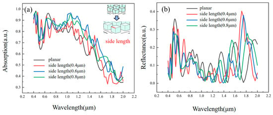
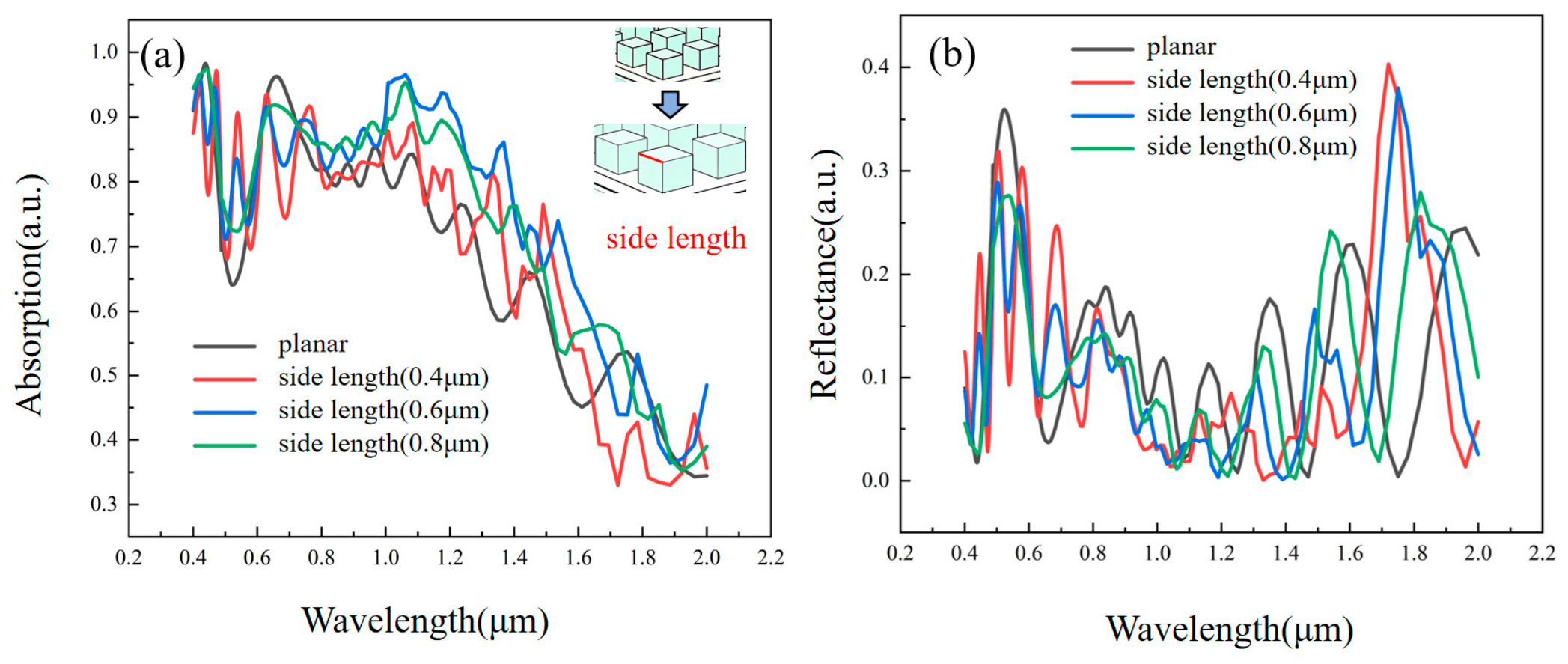
Square and circular pillars, which showed the best morphology-level performance, were selected for univariate lateral-size scans at a fixed height of 0.5 μm. In addition to the baseline side length of 0.5 μm, square-pillar side lengths of 0.4, 0.6, and 0.8 μm were examined, as shown in Figure 4.
Figure 4.
Absorptance (a) and reflectance (b) spectra of square pillars with different side lengths.
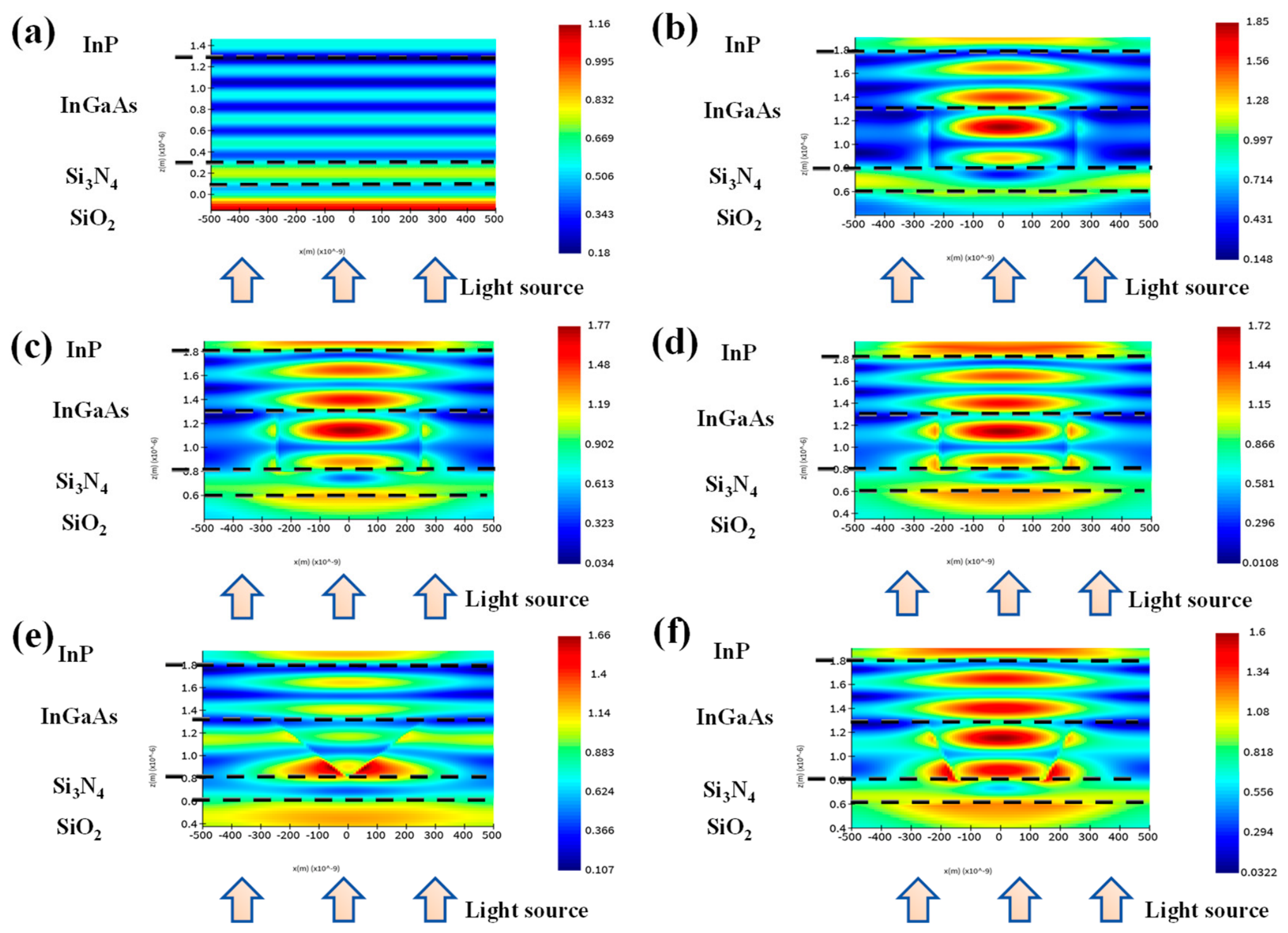
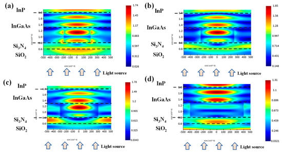
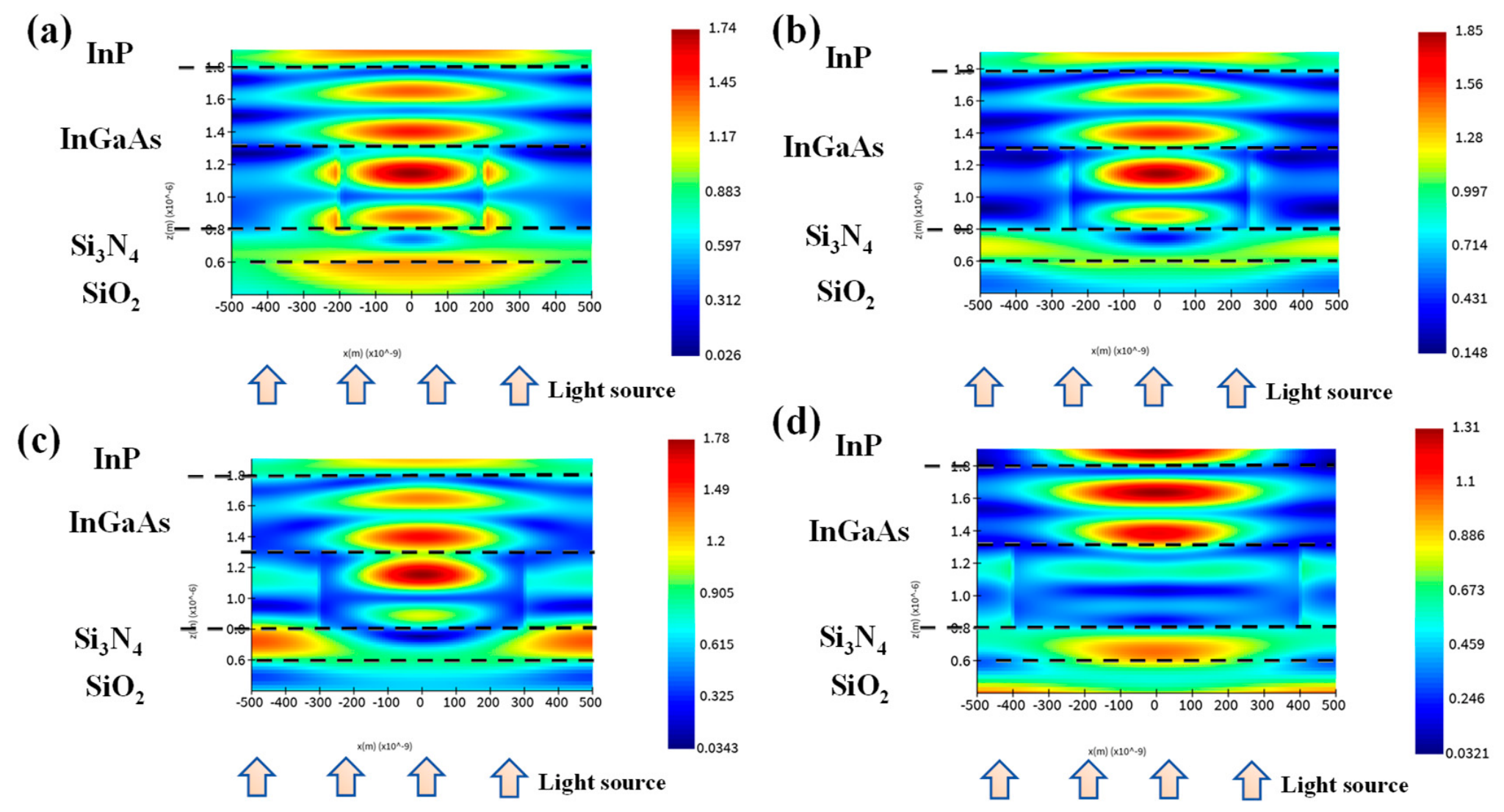
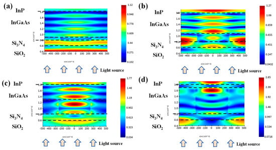
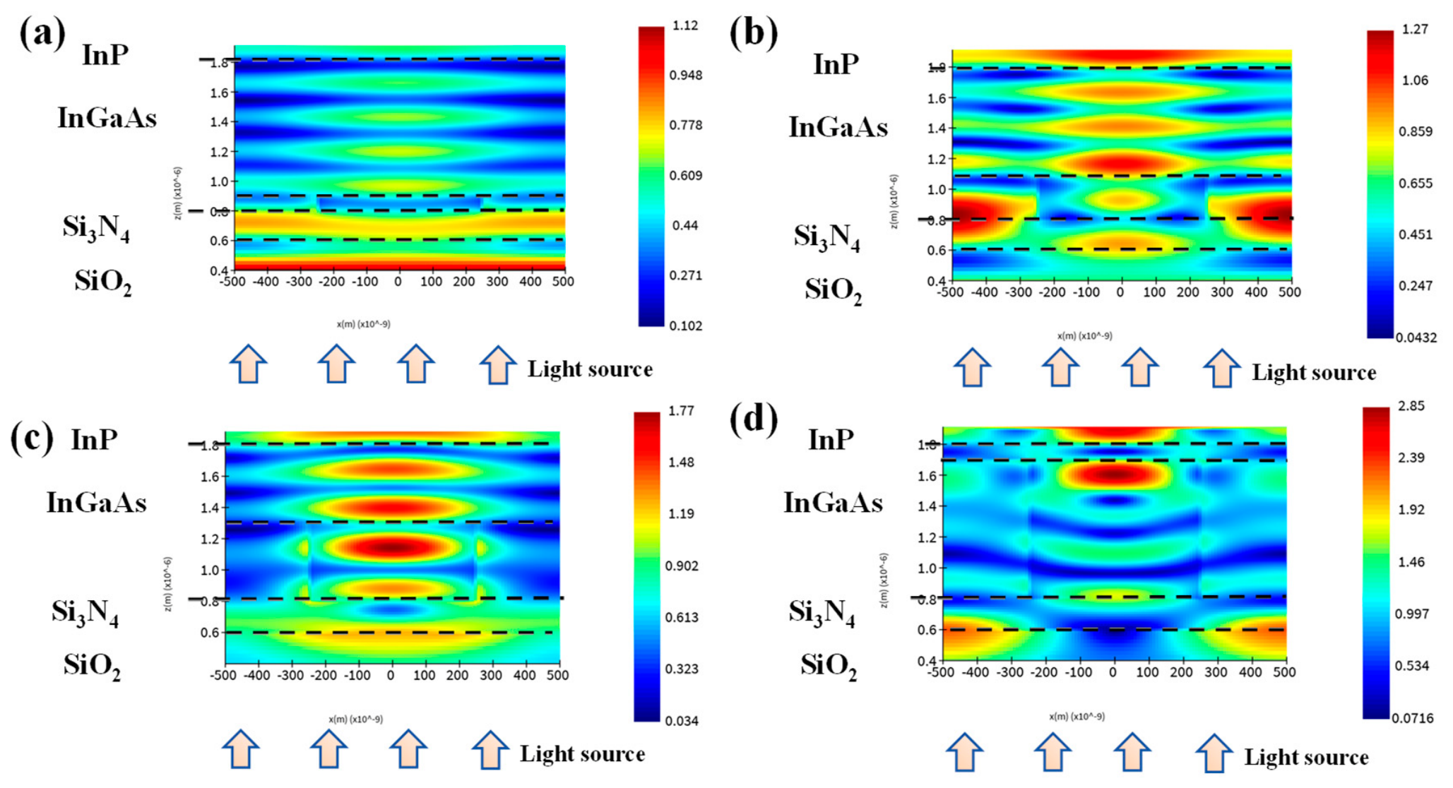
Figure 5 shows the cross-sectional electric-field distributions for square pillars of different side lengths. At 0.4 μm, the pillar is too narrow to sustain strong near-field confinement: the high-field region is limited to a narrow central area, its overlap with the absorption volume is poor, and transmission leakage is severe. At 0.5 μm, the internal standing wave and localized enhancement are pronounced, with a peak field intensity of 1.85, but the energy remains overly concentrated and transmission loss is still high. At the optimal 0.6 μm side length, the central high-field region has a comparable width and a slightly lower peak intensity of 1.78, while strong lateral scattered fields emerge beneath the structure. The transmissivity consequently falls from 0.221 to 0.165. At 0.8 μm, lateral-size mismatch detunes the resonance; the peak field drops to 1.31, high-field regions shift toward the InGaAs surface, reflection increases, and absorptance declines.
Figure 5.
Cross-sectional electric-field distributions for square pillars with side lengths of (a) 0.4 μm, (b) 0.5 μm, (c) 0.6 μm, and (d) 0.8 μm. Color bars are panel-specific, and are not intended for direct quantitative comparison.
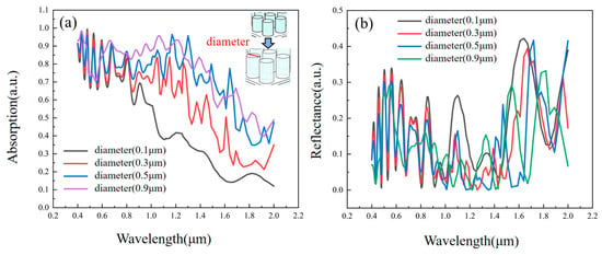
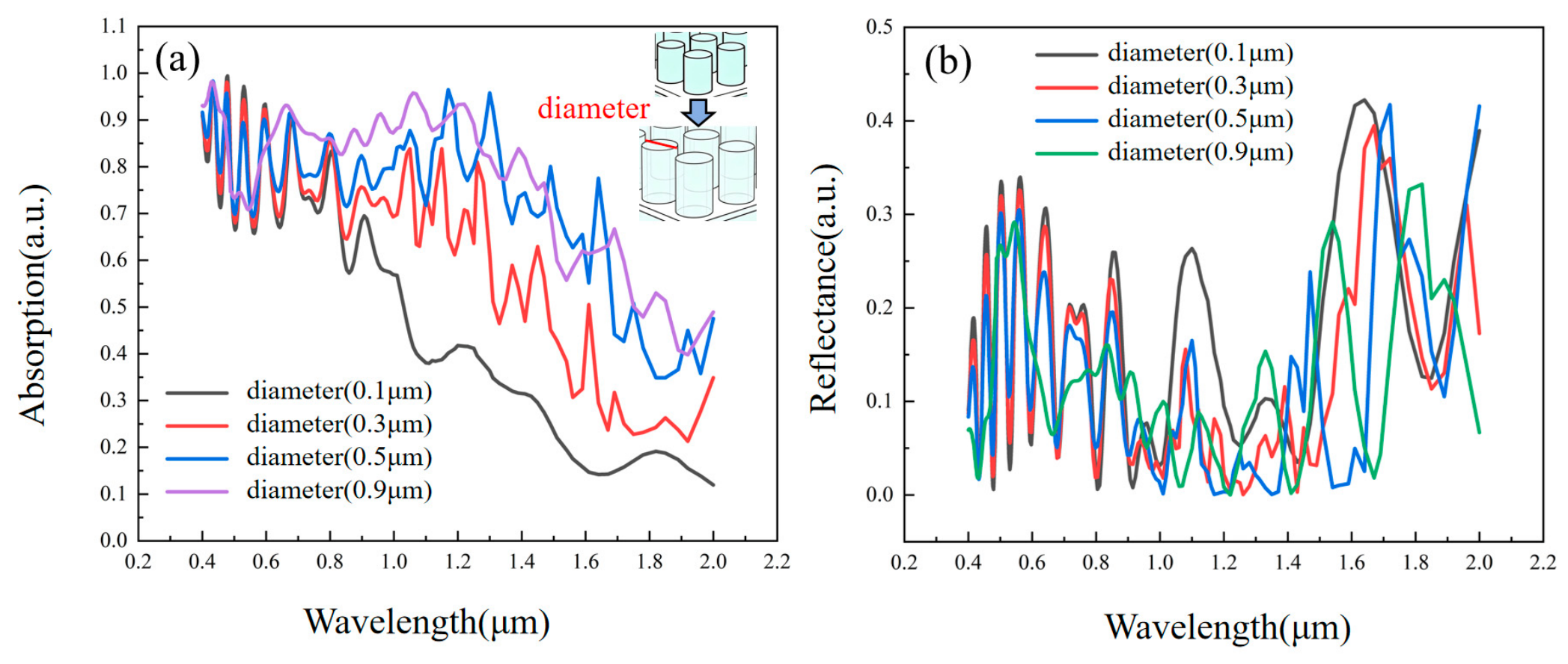
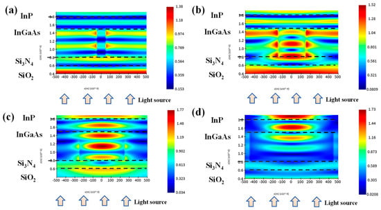
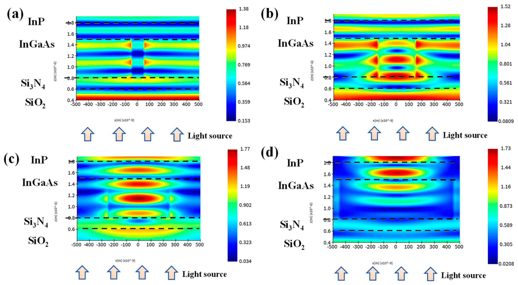
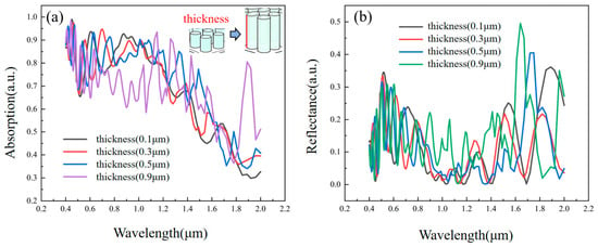
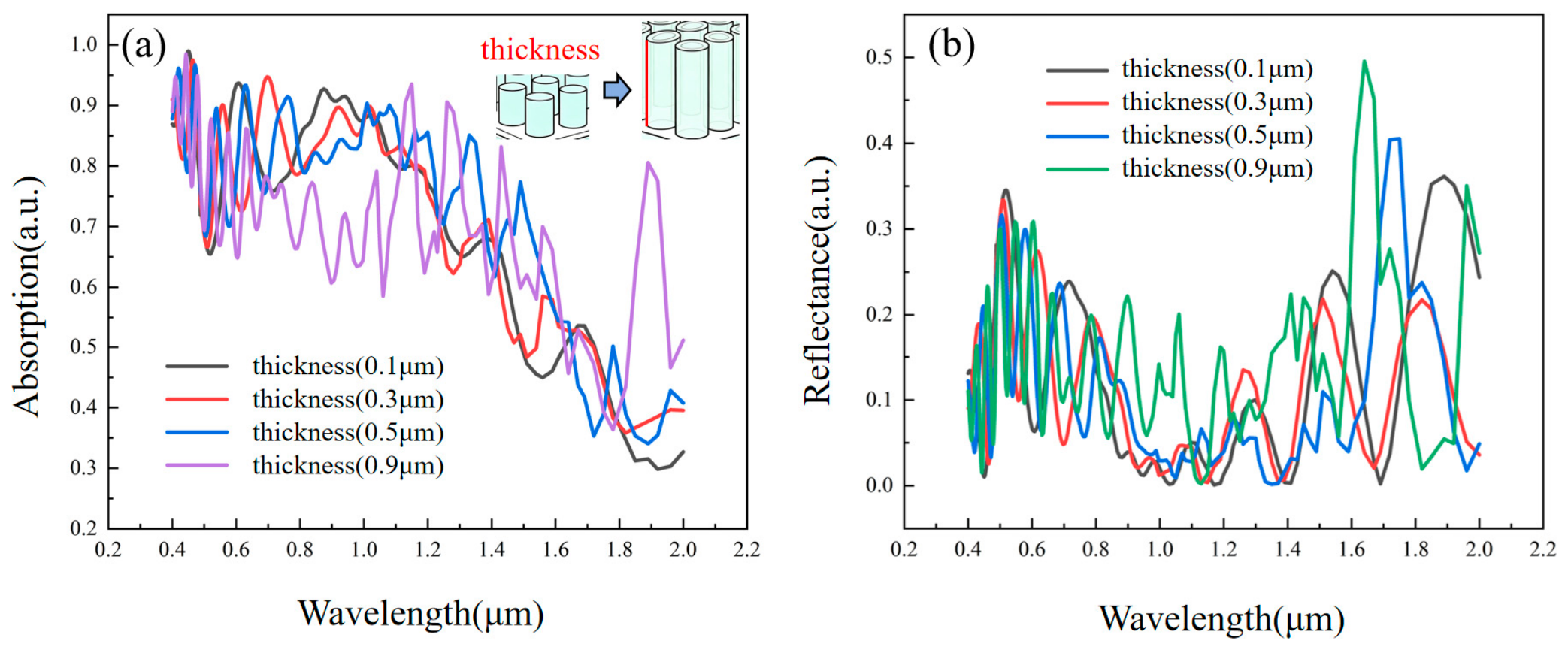
For circular pillars at a fixed height of 0.5 μm, diameters of 0.1, 0.3, 0.5, and 0.9 μm were scanned. The spectra in Figure 6 show the same rise-and-fall dependence of absorptance on lateral size observed for square pillars, confirming that resonance matching is a general feature of columnar morphologies. Across the scan, circular pillars consistently have lower reflectance than comparably sized square pillars, demonstrating the stable antireflection benefit of a curved, graded-index interface.
Figure 6.
Absorption spectra (a) and reflection spectra (b) of circular pillars with different diameters.
Figure 7 shows the electric field distributions of circular pillars with different diameters. At 0.1 μm, the scattering cross-section is too small to induce an effective dielectric resonance; the peak field is only 1.38, the field remains close to the planar standing-wave pattern, and most light is transmitted. At 0.3 μm, the peak field increases to 1.52, and a localized high-field region, longitudinal standing wave, and lateral scattering begin to emerge.
Figure 7.
Cross-sectional electric-field distributions for circular pillars with diameters of (a) 0.1 μm, (b) 0.3 μm, (c) 0.5 μm, and (d) 0.9 μm. Color bars are panel-specific, and are not intended for direct quantitative comparison.
The resonance remains incompletely coupled at 0.3 μm; however, the field coverage is limited and the transmission remains high. At the optimum diameter of 0.5 μm, the peak field reaches 1.77, the internal longitudinal standing wave is well developed, and the curved boundary supports a smooth field transition at the interface.
This combination minimizes interfacial reflection and balances resonance coupling with anti-reflection, yielding the highest absorptance in the univariate diameter scan. At 0.9 μm, the peak field decreases to 1.73 and shifts toward the upper InP/InGaAs interface, reducing the field intensity and the effective absorption-volume integral within InGaAs. Although the reflectivity remains low at this diameter, the reduced field-volume overlap and detuned resonance outweigh the anti-reflection benefit, so the absorptance decreases.
Therefore, square and circular pillars exhibit an optimal lateral-size window for resonance matching, with absorptance increasing and then decreasing as the lateral size grows. When pillars are too small, their scattering cross-section and dielectric-resonance coupling are insufficient, so confinement is weak and transmission leakage is large. At the optimum size, the lateral resonance is matched to 1.55 μm, maximizing large-angle and backward scattering and the field-energy volume integral in the absorber. Oversized pillars detune the resonance, steepen the interfacial refractive-index transition, and shift high-field regions toward the surface, increasing reflection and reducing useful field overlap.
3.3. Height Dependence of Absorptance
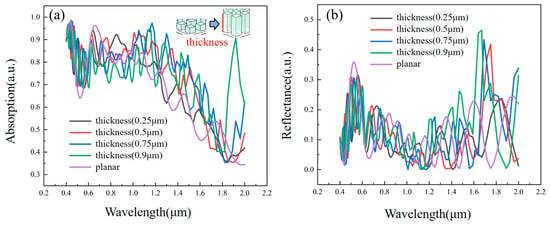
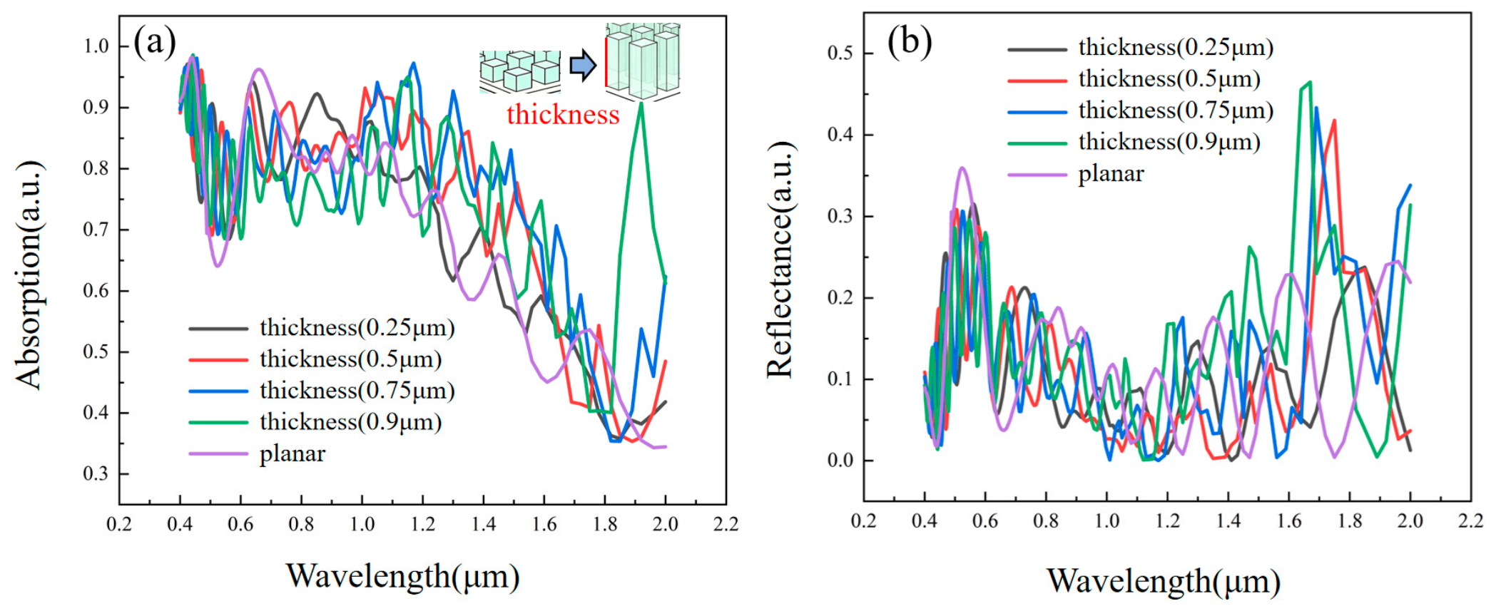
Pillar height governs the vertical field distribution by setting the longitudinal phase accumulation and standing-wave pattern. To complete the geometric parameter study, square pillars with a 0.5 μm side length and circular pillars with a 0.5 μm diameter were independently scanned in height. Their optical spectra and cross-sectional field distributions are shown in Figure 8, Figure 9, Figure 10 and Figure 11.
Figure 8.
Absorptance (a) and reflectance (b) spectra of square pillars with different longitudinal heights.
Figure 9.
Cross-sectional electric-field distributions for square pillars with heights of (a) 0.25 μm, (b) 0.5 μm, (c) 0.75 μm, and (d) 0.9 μm. Color bars are panel-specific, and are not intended for direct quantitative comparison.
Figure 10.
Absorptance (a) and reflectance (b) spectra of circular pillars with different heights.
Figure 11.
Cross-sectional electric-field distributions for circular pillars with heights of (a) 0.1 μm, (b) 0.3 μm, (c) 0.5 μm, and (d) 0.9 μm. Color bars are panel-specific, and are not intended for direct quantitative comparison.
For square pillars, absorptance first increases and then decreases with height. The optimum in this fixed-side-length scan is 0.75 μm, where the 1.55 μm absorptance reaches 0.705 and the reflectance is the lowest in this series, at 0.028. At low heights, the phase accumulation is insufficient to establish a stable longitudinal standing wave, producing disordered fields and substantial transmittance leakage. At 0.75 μm, the structure satisfies the Fabry–Pérot phase-closure condition and supports a stable longitudinal standing-wave pattern, so the high-field region efficiently covers the InGaAs absorber while reflectance and transmittance are minimized. At excessive heights, the resonance detunes and high-field regions concentrate near the upper InP/InGaAs interface. Even when the local field maximum increases, the absorber wide-field integral decreases. Height therefore acts primarily through electromagnetic phase matching and vertical field redistribution, rather than through a simple increase in material volume.
The absorptance and reflectance spectra and cross-sectional field distributions of the circular pillars are shown in Figure 10 and Figure 11. Their height-dependent response follows the same general trend as that of square pillars: absorptance increases rapidly and then saturates or decreases. Increasing height beyond the matching range does not continuously improve absorptance. The curved geometry preserves low reflectance, but dimensional mismatch distorts the field distribution and prevents further suppression of transmittance loss.
The complete lateral-size and height scans show that optical modulation by columnar micro-nanostructures follows a unified dielectric-resonance-matching mechanism, rather than a simple dependence on absorber volume. Lateral size controls Mie-resonance coupling, lateral confinement, and the scattering-angle distribution, thereby suppressing forward transmittance. Height controls Fabry–Pérot phase accumulation and tunes the order and spatial distribution of the longitudinal standing wave, thereby improving coupling of incident light into the absorber.
Both parameters have well-defined resonance-matching windows. Undersized features couple weakly to the incident field and retain high transmittance loss; oversized features detune the resonance, increase interfacial reflectance, and move high-field regions away from the absorption volume. The agreement between the lateral and longitudinal trends confirms that micro-nanostructure absorptance is governed by the spatial field-energy integral in InGaAs. A single-point peak field cannot represent total absorptance: absorptance can decline even when the peak field grows if the high-field region shifts or the resonance becomes mismatched.
For the selected 0.6 μm × 0.9 μm square pillar, a dedicated 1.55 μm complex-field FDTD monitor was placed within the InGaAs pillar (z = 0.30–1.20 μm). The laterally averaged dominant Ex component was fitted to the expression E(z) = E + exp(iβz) + E − exp(−iβz), yielding n_eff = β/k0 = 3.15 with a normalized least-squares residual of 15.4%. The fitted round-trip phase 2βh/(2π) is 3.66, which is close to the longitudinal order m = 4; the net interface-phase correction required for exact phase closure is 2.14 rad modulo 2π. The simulated axial intensity displays four resolved antinodes located at z = 0.399, 0.615, 0.852, and 1.108 μm. Taking a = 0.30 μm as the half-width and adopting the refractive index of bulk InGaAs, the transverse size parameter 2πna/λ equals 4.29. The mean |E|2 inside the pillar is 1.17 times that in the surrounding region, and the lateral center-to-edge intensity ratio at the strongest axial antinode is 9.3. These field and phase metrics confirm that a fundamental-like lateral dielectric resonance is coupled to a near-fourth-order longitudinal standing wave. Since the interface-phase sum is inferred from phase closure, rather than extracted independently, and no isolated-particle multipole decomposition was conducted, the Mie-type label does not assign a unique multipolar mode.
3.4. Coupled Two-Dimensional Scans of Lateral Dimension and Height
The univariate analyses optimized lateral size and height separately while holding the other parameter at its baseline. However, the Mie-resonance and Fabry–Pérot phase conditions are not fully independent: the lateral cross-section determines the effective refractive index and modal volume seen by the longitudinal standing wave, whereas height changes the near-field distribution and in-plane coupling. Two-dimensional coupled scans were therefore performed to resolve these interactions and locate the sampled optima. Square-pillar side lengths of 0.4, 0.5, 0.6, and 0.8 μm were combined with heights of 0.25, 0.5, 0.75, and 0.9 μm. Circular-pillar diameters of 0.1, 0.3, 0.5, and 0.9 μm were combined with heights of 0.1, 0.3, 0.5, and 0.9 μm. These are discrete design points from the completed simulation matrix, not a continuous sweep; 0.7 μm was omitted as a sampling choice in the present dataset, so no 0.7 μm value is inferred or reported. The absorptance at 1.55 μm for each simulated combination is listed in Table 2 and Table 3.
Table 2.
Absorptance at 1.55 μm for square-pillar arrays in two-dimensional side-length and height scans.
Table 3.
Absorptance at 1.55 μm for circular-pillar arrays in the two-dimensional diameter and height scans.
The square-pillar scan in Table 2 reveals strong parameter coupling. The global optimum is a side length of 0.6 μm and a height of 0.9 μm, giving an absorptance of 0.749. This is higher than the baseline value of 0.685 (0.5 μm × 0.5 μm), the univariate lateral optimum of 0.715 (0.6 μm × 0.5 μm), and the univariate height optimum of 0.705 (0.5 μm × 0.75 μm). At a 0.6 μm side length, absorptance rises from 0.539 at 0.25 μm height to 0.749 at 0.9 μm height, indicating that the wider pillar benefits from greater longitudinal phase accumulation. By contrast, at 0.5 μm side length, absorptance peaks at 0.75 μm height (0.705) and falls to 0.650 at 0.9 μm, confirming that the optimum height depends on lateral size. The 0.8 μm pillars remain comparatively weak at all heights (maximum 0.626), indicating a lateral detuning that cannot be corrected by height adjustment.
For circular pillars, Table 3 shows a nonmonotonic coupled response. At a fixed diameter, absorptance generally increases with height over 0.5–0.9 μm before saturating or decreasing, consistent with longitudinal Fabry–Pérott matching. At a fixed height, absorptance increases with diameter at a rate that depends on height. The global optimum is a diameter of 0.9 μm and a height of 0.9 μm, yielding an absorptance of 0.682, above the univariate optimum of 0.640 at 0.5 μm diameter and 0.5 μm height. At 0.1 μm diameter, absorptance remains below 0.436 at every height, confirming that longitudinal tuning cannot compensate for an inadequate scattering cross-section. At 0.5 μm diameter, the identical value of 0.640 at 0.5 and 0.9 μm indicates a comparatively robust resonance regime.
Across the two-dimensional scans, square pillars provide the highest absorptance under the present fixed-nominal-dimension comparison: the maximum absorptance is 0.749 versus 0.682, and even the lowest square-pillar result (0.528 at 0.8 μm × 0.25 μm) remains competitive with mid-range circular configurations. This comparison does not fully isolate morphology, because the square- and circular-pillar configurations have different fill factors and absorber volumes; a controlled equal-fill-factor or equal-volume comparison would be needed to assign the residual difference to shape alone. Lateral size sets the Mie-resonance strength and modal volume, whereas height sets Fabry–Pérot phase accumulation. Near their joint optimum, electromagnetic energy is confined laterally by dielectric resonance and vertically by standing-wave closure, maximizing the |E|2 volume integral within InGaAs. The two-dimensional scan therefore identifies a coupled region of parameter space, rather than two independent single-parameter optima.
To assess whether the selected 0.6 μm × 0.9 μm square pillar compromises the working band, the normalized absorptance was integrated over 0.9–1.7 μm using the trapezoidal rule, as follows:
where denotes the spectrally averaged absorptance over the 0.9–1.7 μm short-wave infrared band, and A(λ) is the wavelength-dependent absorptance. Over 0.9–1.7 μm, the mean absorptance values are 0.672 for the planar reference, 0.829 for the selected square pillar, and 0.826 for the selected circular pillar, corresponding to gains of 23.4% and 22.9% for the square- and circular-pillar structures, respectively, as shown in Table 4.
Table 4.
Mean absorptance over 0.9–1.7 μm for the planar and optimized structures.
3.5. Carrier Transport and Collection Performance
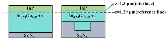
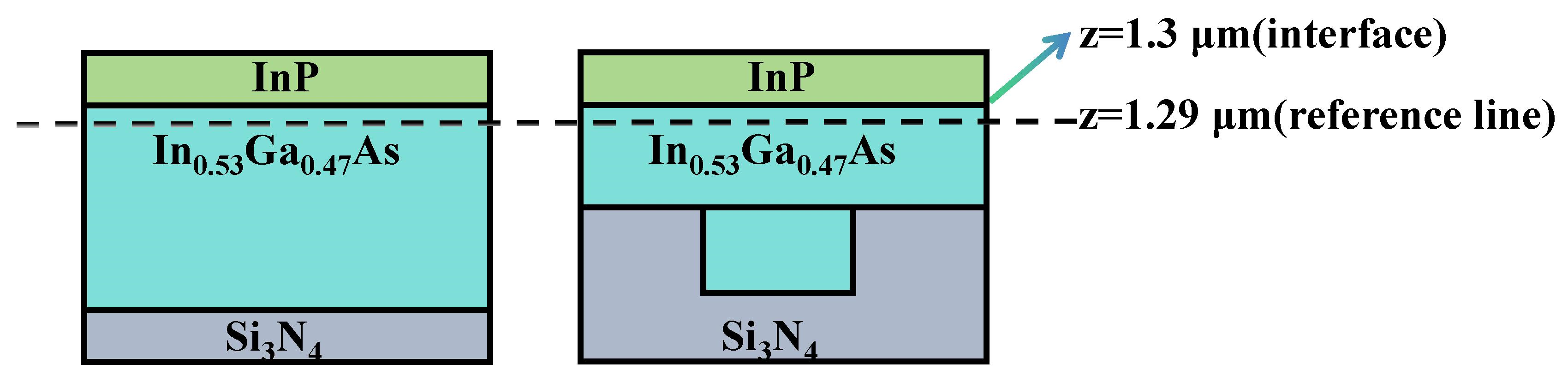
The absolute carrier concentrations along the reference line are similar for the two structures. The mean electron concentration changes from 9.016 × 105 cm−3 in the planar structure to 9.106 × 105 cm−3 in the compact square pillar, while the mean hole concentration changes from 2.819 × 10¹⁷ to 2.776 × 1017 cm−3. The line lies in the common upper InGaAs layer, 10 nm below the z = 1.30 μm interface, and therefore samples a single local position rather than the whole absorber, whereas the additional patterned absorber and imported generation enhancement occur lower in the structured unit cell, as shown in Figure 12.
Figure 12.
Schematic diagram of reference-line positions.
Under the normalized output scale, the internally collected carrier-rate proxy increases from 2.742 × 10⁷ to 4.826 × 10⁷, representing a 76.1% rise. This proxy denotes carriers that reach the modeled InP/InGaAs-side collection boundary under a 5 V contact bias; it does not represent electrons emitted into vacuum.
For the 0.6 μm × 0.9 μm square pillar selected in this manuscript, the geometry-matched FDTD generation profile was imported into a matched two-dimensional CHARGE geometry under the same specified 5 V bias. The normalized integrated generation is 7.097 × 10⁷ and the collected proxy is 4.826 × 10⁷, corresponding to increases of 29.2% and 76.1%, respectively, relative to the planar reference.
The recombination results further clarify the scope of this comparison. Under the identical ideal-sidewall condition (sidewall SRV = 0), the CHARGE outputs integrated over the InGaAs absorber give SRH recombination rates of 1.34893 × 10⁴ and 1.40010 × 10⁴ pairs s−1, Auger rates of 5.30292 × 10⁶ and 5.21724 × 10⁵ pairs s−1, and radiative rates of 9.95239 × 10³ and 1.31234 × 10³ pairs s−1 for the planar and square-pillar structures, respectively, corresponding to pillar-to-planar ratios of 1.0379, 0.09838, and 0.13186, as shown in Table 5. The previously quoted values of 0.098 and 0.132 were the Auger and radiative pillar-to-planar ratios, respectively, and are now reported together with their absolute integrated rates. Both reductions originate in the lower p+ region (0.3 ≤ z < 0.5 μm), which supplies 99.97%/99.90% of the two Auger integrals and 96.87%/75.85% of the two radiative integrals. Within this region, the lateral width is 1.0 μm in the planar model and 0.2 μm in the pillar model, and the mean Auger rate also falls to 0.491 of the planar value, so that 0.20005 × 0.49085 ≈ 0.098 reproduces the near-90% Auger reduction, whereas the radiative contribution outside this footprint raises the radiative ratio to 0.132. Reintegrating the generation fields gives 1.31283 × 10⁷ and 1.20868 × 10⁷ pairs s−1 in this same lower region, i.e., a decrease, while the generation above z = 0.5 μm increases from 4.19851 × 10⁷ to 5.90132 × 10⁷ pairs s−1, which reconciles the 29.2% total increase with the locally reduced high-loss footprint. Similarity along a single reference line does not constrain these volume-integrated quantities [25,26,27], because Auger and radiative recombination depend nonlinearly on the local carrier densities and are evaluated over the entire absorber. The reported integrals also exclude the additional sidewall SRH term. Hence, the values should be interpreted as ideal-sidewall reference values. Importantly, the substantial reduction in Auger and radiative recombination observed between the two configurations arises predominantly from geometry-dependent shrinkage of the heavily-doped bottom p+ contact footprint, and cannot be attributed purely to optical light-trapping effects. In the present setup, the p+ contact is conformally patterned underneath the nanostructured mesa, representing a realistic fabrication scenario. A comparative simulation maintaining full-width p+ contact identical to the planar baseline is outside the present dataset, and will be addressed in follow-up work. Accordingly, the present result supports only a matched, ideal-passivation comparison, and does not make predictions for an experimentally processed device, which would require the intended doping profile, contact conditions, material parameters, and measured sidewall SRVs.
Table 5.
Normalized FDTD-to-CHARGE carrier-collection metrics for the compact 0.6 μm × 0.9 μm square-pillar audit at 1.55 μm and 5 V bias.
To estimate the sidewall SRV at which the carrier-collection advantage of the nanostructure vanishes, we introduce a first-order effective-loss model. The SRV-dependent collection efficiency of the pillar is written as
where ηC,0 = 0.680 is the calculated pillar collection efficiency for zero sidewall recombination, kb is an effective bulk loss rate, and As/VInGaAs = 3.46 × 104 cm−1. The zero-gain condition is obtained by equating the internally collected carrier rates of the pillar and planar structures:
GpillarηC(Sth) = GplanarηC,planar.
Because Gpillar/Gplanar = 7.097 × 10⁷/(5.495 × 107) = 1.292 and ηC,planar = 0.499, the pillar efficiency at the zero-gain point is ηC(Sth) = 0.499/1.292 = 0.386.
For kb = 1 × 10⁷ s−1, this gives Sth ≈ 2.2 × 102 cm s−1. To account for the uncertainty associated with representing the combined bulk recombination channels by a single effective rate, we additionally consider kb = 4 × 10⁷ s−1, corresponding to an effective decay time on the order of tens of nanoseconds and consistent with the decay-rate scale reported for passivated InGaAs/InP nanostructures [24]. This yields Sth ≈ 8.8 × 102 cm s−1. Within this first-order model, the estimated zero-gain SRV is therefore approximately 2.2 × 10²–8.8 × 102 cm s−1. The reported value S = 260 cm s−1 for strongly passivated InGaAs/InP nanopillars lies close to the lower end of this interval, and should therefore be regarded as a near-threshold reference: it may preserve a positive collection gain for a larger effective bulk-loss rate, but it does not guarantee a positive gain for all possible bulk-recombination conditions. The optical absorptance enhancement remains an FDTD result, whereas the corresponding carrier-collection enhancement is further limited by sidewall recombination. Because the present laterally averaged two-dimensional model does not explicitly resolve the sidewall boundary, the calculated threshold should be interpreted as an order-of-magnitude estimate, rather than as an exact three-dimensional device value.
Note that the 35.4% increase in total structure absorptance differs from the 29.2% increase in integrated photogeneration. Total absorptance includes absorption in all layers of the stack, whereas photogeneration arises only in the InGaAs absorber; the nanostructure-induced redistribution of optical energy between active and parasitic layers accounts for the difference. The three recombination quantities are integrals over the InGaAs absorber obtained from the same matched CHARGE run and exclude any sidewall recombination term. The carrier-collection quantities are internal semiconductor metrics, and do not include photoelectron escape into a vacuum.
4. Conclusions
This work combines FDTD and drift-diffusion simulations to quantify micro-nanostructures light trapping and semiconductor carrier collection in transmission-mode InGaAs photocathodes with a fixed total absorber thickness. Among the tested structures, square pillars achieve the best baseline balance among reflectance, transmittance, and field overlap. Coupled scans identify a maximum absorptance of 0.749 for square pillars with a side length of 0.6 μm and a height of 0.9 μm, and a maximum absorptance of 0.682 for circular pillars with a diameter of 0.9 μm and a height of 0.9 μm. These observed trends originate from the combined effect of graded effective index, dielectric-resonance confinement, scattering, Fabry–Pérot phase matching, and fill factor. Under normalized illumination with a 5 V bias, a separately normalized compact-baseline transport comparison shows a 29.2% increase in integrated generation. The internal generation-rate-weighted collection efficiency ηC reaches 0.680, compared with 0.499 for the planar structure, and the normalized internally collected carrier-rate proxy increases by 76.1%. All of these results are simulated under ideal sidewall passivation and normal-incidence illumination; specifically, the 76.1% enhancement in internally collected carrier-rate proxy is an ideal upper-limit value; real devices will suffer non-negligible performance degradation originating from sidewall surface recombination, as well as additional losses under off-angle incidence. Because the morphology sweep does not fully decouple fill factor and absorber volume from shape, the reported morphology ranking should be interpreted as a geometry-level comparison; equal-fill-factor/equal-volume controls are needed to isolate shape-specific effects. We further note that the large differences in Auger and radiative recombination between planar and nanostructured devices are partly driven by the changed lateral footprint of the bottom p+ contact, rather than originating solely from optical light-trapping. Despite these idealized boundaries, the present optical-electrical co-optimization provides promising structural guidelines for enhancing photon absorption in transmission-mode InGaAs photocathodes. This study lays a theoretical foundation for follow-up work, including nanofabrication validation of the proposed micro-nanostructures, oblique-incidence performance evaluation, and complete device modeling incorporating surface photoelectron-emission dynamics.
Author Contributions
Conceptualization, H.Q. and F.S.; methodology, H.Q.; software, L.C.; validation, Q.Z. and J.D.; formal analysis, H.Q.; investigation, S.L. and X.H.; resources, D.D.; data curation, H.C.; writing—original draft preparation, H.Q.; writing—review and editing, F.S. and L.C.; visualization, Q.Z.; supervision, F.S.; project administration, H.Q.; funding acquisition, F.S. All authors have read and agreed to the published version of the manuscript.
Funding
This research received no external funding.
Data Availability Statement
The original contributions presented in this study are included in the article. Further inquiries can be directed to the corresponding author.
Conflicts of Interest
The authors declare no conflict of interest.
References
- Jing, W.J.; Deng, J.; Zhu, Y.; Zhang, Y.; Ye, J.; Zhou, J.; Chen, X. Monolithic High-Accuracy Long-Wave Infrared Full-Stokes Polarimeter Based on a Meta-QWIP. Laser Photonics Rev. 2025, 20, e01411. [Google Scholar] [CrossRef] [Scilit]
- Campbell, J.C. Recent advances in avalanche photodiodes. J. Light. Technol. 2016, 34, 278–285. [Google Scholar] [CrossRef] [Scilit]
- Yu, C.; Xu, Q.; Zhang, J. Recent advances in InGaAs/InP single-photon detectors. Meas. Sci. Technol. 2024, 35, 122003. [Google Scholar] [CrossRef] [Scilit]
- Zhu, T.; Wang, L.; Jing, W.; Deng, J.; Ye, J.; Zhang, Y.; Chu, Z.; Zhou, J.; Chen, X.; Li, X.; et al. Circular Polarimetric Imaging with a Metamaterial Integrated Long-Wavelength Infrared Focal Plane Array. Adv. Sci. 2025, 12, e09292. [Google Scholar] [CrossRef] [Scilit] [PubMed]
- Pastuszka, S.; Hoppe, M.; Kratzmann, D.; Schwalm, D.; Wolf, A.; Jaroshevich, A.S.; Kosolobov, S.N.; Orlov, D.A.; Terekhov, A.S. Preparation and performance of transmission-mode GaAs photocathodes as sources for cold dc electron beams. J. Appl. Phys. 2000, 88, 6788–6800. [Google Scholar] [CrossRef] [Scilit]
- Lee, H.; Cultrera, L.; Bazarov, I. Intrinsic emittance reduction in transmission mode photocathodes. Appl. Phys. Lett. 2016, 108, 124105. [Google Scholar] [CrossRef] [Scilit]
- Jin, X.; Yamamoto, N.; Nakagawa, Y.; Mano, A.; Kato, T.; Tanioku, M.; Ujihara, T.; Takeda, Y.; Okumi, S.; Yamamoto, M.; et al. Super-high brightness and high-spin-polarization photocathode. Appl. Phys. Express 2008, 1, 045002. [Google Scholar] [CrossRef] [Scilit]
- Zhou, R.; Jani, H.; Zhang, Y.; Qian, Y.; Duan, L. Photoelectron transportation dynamics in GaAs photocathodes. J. Appl. Phys. 2021, 130, 113101. [Google Scholar] [CrossRef] [Scilit]
- Brongersma, M.L.; Cui, Y.; Fan, S. Light management for photovoltaics using high-index nanostructures. Nat. Mater. 2014, 13, 451–460. [Google Scholar] [CrossRef] [Scilit] [PubMed]
- Kuznetsov, A.I.; Miroshnichenko, A.E.; Brongersma, M.L.; Kivshar, Y.S.; Luk’yanchuk, B. Optically resonant dielectric nanostructures. Science 2016, 354, aag2472. [Google Scholar] [CrossRef] [Scilit] [PubMed]
- Van de Groep, J.; Polman, A. Designing dielectric resonators on substrates: Combining magnetic and electric resonances. Opt. Express 2013, 21, 26285–26302. [Google Scholar] [CrossRef] [Scilit] [PubMed]
- Xu, R.; Morimoto, T.; Takahara, J. Vertical photon sorting by stacking silicon and germanium nanopillars for broadband absorbers. Nanophotonics 2023, 12, 2461–2469. [Google Scholar] [CrossRef] [Scilit] [PubMed]
- Allayarov, I.; Aita, V.; Roth, D.J.; van Casteren, B.; Bykov, A.Y.; Evlyukhin, A.B.; Zayats, A.V.; Lesina, A.C. Strong coupling of collective optical resonances in dielectric metasurfaces. Light Sci. Appl. 2025, 14, 387. [Google Scholar] [CrossRef] [Scilit] [PubMed]
- Roy, D.; Samajdar, D.P.; Biswas, A. Photovoltaic performance improvement of GaAs1−xBix nanowire solar cells in terms of light trapping capability and efficiency. Sol. Energy 2021, 221, 468–475. [Google Scholar] [CrossRef] [Scilit]
- Peng, X.; Zhong, C.; Zou, J.; Deng, W. All-dielectric meta-surface transmission-mode ultra-thin GaAs negative electron affinity photocathode. Appl. Phys. Lett. 2024, 125, 071103. [Google Scholar] [CrossRef] [Scilit]
- Li, S.; Zhang, Y.; Tang, S.; Yang, L.; Ma, X.; Gao, J.; Tong, Z.; Qian, Y.; Shi, F.; Guo, X. Near-infrared enhancement in thin transmission-mode GaAs photocathodes via nanostructured window layer. Opt. Express 2025, 33, 38543–38552. [Google Scholar] [CrossRef] [Scilit] [PubMed]
- Zhang, H.; Tian, Y.; Li, Q.; Ding, W.; Yu, X.; Lin, Z.; Feng, X.; Zhao, Y. Photon-Trapping Microstructure for InGaAs/Si Avalanche Photodiodes Operating at 1.31 μm. Sensors 2022, 22, 7724. [Google Scholar] [CrossRef] [Scilit] [PubMed]
- Dong, H.; Wu, Y.; Zheng, H.; Chen, P.; Deng, W.; Ma, L.; Dong, X.; Duan, Z.; Li, M. Design and Simulation of a High-Responsivity Dielectric Metasurface Si-Based InGaAs Photodetector. Photonics 2024, 11, 906. [Google Scholar] [CrossRef] [Scilit]
- Palik, E.D. Handbook of Optical Constants of Solids, Volume III; Academic Press: San Diego, CA, USA, 1998. [Google Scholar]
- Kikuta, H.; Ohira, Y.; Kubo, H.; Iwata, K. Effective medium theory of two-dimensional subwavelength gratings in the non-quasi-static limit. J. Opt. Soc. Am. A 1998, 15, 1577–1586. [Google Scholar] [CrossRef] [Scilit]
- Ünlü, M.S.; Strite, S. Resonant cavity enhanced photonic devices. J. Appl. Phys. 1995, 78, 607–639. [Google Scholar] [CrossRef] [Scilit]
- Jeddi, H.; Adham, K.; Zhao, Y.; Witzigmann, B.; Römer, F.; Bermeo, M.; Borgström, M.T.; Pettersson, H. Enhanced LWIR response of InP/InAsP quantum discs-in-nanowire array photodetectors by photogating and ultra-thin ITO contacts. Nanotechnology 2024, 35, 215206. [Google Scholar] [CrossRef] [Scilit] [PubMed]
- Labiod, S.; Smaani, B.; Tayal, S.; Rahi, S.B.; Sedrati, H.; Latreche, S. Mixed-mode optical/electric simulation of silicon lateral PIN photodiode using FDTD method. Silicon 2023, 15, 1181–1191. [Google Scholar] [CrossRef] [Scilit]
- Higuera-Rodriguez, A.; Romeira, B.; Birindelli, S.; Black, L.E.; Smalbrugge, E.; van Veldhoven, P.J.; Kessels, W.M.M.; Smit, M.K.; Fiore, A. Ultralow Surface Recombination Velocity in Passivated InGaAs/InP Nanopillars. Nano Lett. 2017, 17, 2627–2633. [Google Scholar] [CrossRef] [Scilit] [PubMed]
- Sze, S.M.; Ng, K.K. Physics of Semiconductor Devices, 3rd ed.; Wiley-Interscience: Hoboken, NJ, USA, 2006. [Google Scholar] [CrossRef] [Scilit]
- Hall, R.N. Electron-hole recombination in germanium. Phys. Rev. 1952, 87, 387–396. [Google Scholar] [CrossRef] [Scilit]
- Shockley, W.; Read, W.T., Jr. Statistics of the recombinations of holes and electrons. Phys. Rev. 1952, 87, 835–842. [Google Scholar] [CrossRef] [Scilit]

Disclaimer/Publisher’s Note: The statements, opinions and data contained in all publications are solely those of the individual author(s) and contributor(s) and not of MDPI and/or the editor(s). MDPI and/or the editor(s) disclaim responsibility for any injury to people or property resulting from any ideas, methods, instructions or products referred to in the content. |
© 2026 by the authors. Licensee MDPI, Basel, Switzerland. This article is an open access article distributed under the terms and conditions of the Creative Commons Attribution (CC BY) license.