


Abstract
LiDAR is a key sensor for depth perception in applications ranging from autonomous vehicles and industrial robotics to robotic vacuum cleaners and topographic mapping, with its depth resolution determined by the timing electronics. This article, to the best of our knowledge, presents the first implementation of an FPGA-based time-to-amplitude converter (TAC) in a LiDAR system alongside the first integration of walk error compensation into such an architecture. The threshold-crossing time shifts with the echo amplitude, causing walk error. This walk error can reach tens of centimeters depending on target reflectivity and range. Pulse-width-based correction has been demonstrated, but reported implementations obtain the time-of-flight (ToF) and the pulse width with time-to-digital converters (TDCs), whose high resolution relies on high-speed clocks for coarse time and delay lines for fine-time measurements, which suffer from coarse-count ambiguity, bin calibration requirements, sensitivity to process, voltage, and temperature (PVT) variations, and portability limitations. This article enhances the novel FPGA-based TAC previously introduced by the authors for pulse-width-based walk error compensation without using a clock or a delay line. Each ToF channel requires only one D flip-flop in the FPGA and a low-cost external passive circuit coupled to the multichannel analog-to-digital converter (ADC) of the FPGA. Using our FPGA-based TAC in our LiDAR experimental setup, the walk-induced distance error is successfully reduced from 42 cm to 2 cm, and target distances of up to 3 m are measured within a 2 cm maximum error.
1. Introduction
In pulsed time-of-flight (ToF) LiDAR, the distance to a target is obtained from the delay between an emitted laser pulse and its echo, and a timing error of 1 ns corresponds to a range error of 15 cm. The delay is measured either directly, with a time-to-digital converter (TDC) that time-stamps the edges of the pulses, or indirectly, with a time-to-amplitude converter (TAC) that converts the phase shift between the transmitted and received pulses into a voltage, which is subsequently sampled by an analog-to-digital converter (ADC) [1]. The TAC-based measurement, therefore, belongs to the indirect ToF (iToF) class, as in iToF sensors, which integrate many illumination periods. Therefore, the delay is not time-stamped but integrated over many pulses into a duty-cycle-proportional voltage. The transmitter, however, still emits short pulses that are detected with a leading-edge comparator, so the amplitude-dependent shift of the detection instant, the walk error introduced below, is effective. Most TDCs follow the Nutt interpolation method [2]: a coarse counter driven by a reference clock covers the measurement range, and a fine interpolator resolves the fraction of a clock period. In FPGAs, the interpolator is usually a tapped delay line (TDL) built from carry-chain elements [3], a Vernier delay line [4], or a set of phase-shifted clocks [5]. In our previous work, a 32-channel TDC based on dynamic phase shifting (DPS) was realized with very low logic utilization [6].
High-performance TACs, in contrast, have mostly been realized as application-specific integrated circuits (ASICs), for example, SiGe BiCMOS converters for time-correlated single-photon counting [7,8], CMOS converters for single-photon ToF measurement [9] and diffuse optical tomography [10], and on-chip time-to-voltage converters in specialized LiDAR receiver ICs [11]. We have previously shown that a TAC can also be constructed from an FPGA lookup table (LUT) configured as an XOR gate alongside a simple passive RC low-pass filter and buffer [12]. That converter resolved 18 ps phase steps; its output for a 2304 ps interval changed by only 3.3 mV (corresponding to ~32 ps) between 3 °C and 93 °C, and by at most 2.2 mV for supply voltages ranging from ±3.5 V to ±10 V.
In leading-edge timing discrimination, the received electrical echo signal is compared against a fixed threshold. Because the received optical power varies widely with target distance and surface reflectivity, pulses of different amplitudes cross this threshold at different instants [13,14,15]. The resulting walk error can easily reach several nanoseconds. When the XOR-based TAC of [12] was evaluated in our laboratory LiDAR setup, echo-power variations severely degraded the ranging accuracy, shifting the measured distance by over 40 cm. The same setup also revealed that the XOR detector fails once the transmitted pulse width is shorter than the ToF. These two limitations directly motivated the present work.
Walk error can be compensated by measuring the echo amplitude using a high-speed, high-precision peak detector or a peak-detect-and-hold circuit [16,17]. However, such circuits lose amplitude distinction once the preamplifier saturates, demanding auxiliary analog circuitry, such as dual-gain or logarithmic stages, to extend amplitude-based correction into the saturation regime [18]. Constant-fraction and zero-crossing discriminators, often combined with automatic gain control, reduce the amplitude dependence of the timing point but require additional high-speed analog circuitry and remain sensitive to pulse clipping [19,20,21]. Dual-threshold methods extrapolate the arrival time from two threshold crossings [22]; integrated receivers have implemented related schemes with constant-delay detection [23] or with a slew-rate measurement from two thresholds [24], which introduces an inherent trade-off between threshold spacing and dynamic range.
A prominent alternative is to estimate the echo intensity from the width of the comparator output, i.e., from the time over threshold (ToT). Kurtti and Kostamovaara showed that the pulse width remains a monotonic function of the echo amplitude even when the receiver is driven into saturation [25] and used it in integrated receivers read out by multichannel CMOS TDCs [26,27]; later designs combined the pulse width with the rise time and reached millimeter-level residual walk over dynamic ranges of 1:40,000 to 1:100,000 [28,29]. Choe et al. combined ToT with a slew-rate estimate to account for the shape of the reflecting surface [30], and pulse-width correction has also been implemented with commercial TDC chips [31,32] and with our DPS-based FPGA TDC [6]. Using the echo pulse width to correct walk error is, therefore, an established principle, and this work leverages this concept rather than claiming it as an original contribution.
In all of these implementations, however, the ToF and the pulse width are obtained with TDCs, and most high-resolution TDCs, whether an ASIC or an FPGA design, depend on the same two ingredients: a high-speed reference clock for the coarse count and a delay line for the fine interpolation [2]. However, each brings its own error mechanisms. Because input events are asynchronous to the clock, the coarse counter and the fine time interpolator must be synchronized. Otherwise, an event occurring close to a clock edge can be registered in an adjacent cycle, introducing a ±1 clock cycle coarse-count ambiguity caused by internal clock-domain crossing and routing skew between the counter and delay elements [33,34]. Furthermore, the clock adds its jitter and distribution skew to every timestamp. The delay line resolves time with the propagation delay of its elements, which varies with process, voltage, and temperature (PVT). Propagation delay values also depend on physical placement within the fabric: delay lines placed at different locations across the same FPGA die exhibit noticeable delay mismatches, and on our Artix-7 device, the delay of a carry cell changed between 17.85 ps and 21.7 ps from −30 °C to 105 °C [12]. The bins, therefore, have to be characterized one by one, with a code density test or a phase sweep, and recalibrated whenever temperature drifts [35,36]. ASIC TDCs face the same process dependence of their delay elements and, in addition, require the complex design and fabrication cycles of custom silicon. A TAC needs neither a clock nor a delay line in the measurement path: the interval is converted into a duty cycle by logic driven directly by the input edges and averaged by an RC filter, so its resolution and linearity are set by the logic voltage levels and passive components rather than by delay cells. The XOR-based TAC of [12], however, cannot be used for walk error compensation, since the amplitude-dependent broadening of the echo highly deviates the ToF measurement, as shown in Section Walk Error Simulations.
In this article, the FPGA-based TAC of [12] is redesigned and enhanced specifically for walk error compensation in pulsed LiDAR. Its XOR gate is replaced by a D flip-flop (DFF) that is set by the transmitted pulse and asynchronously cleared by the leading edge of the echo, so that the DFF output carries only the leading-edge ToF, independent of the echo width, while the echo width itself is converted in a second, structurally identical buffered RC low-pass filter channel and serves as the compensation variable. In the FPGA, a ToF channel occupies a single DFF, whereas a pulse-width channel consumes no logic resources at all; outside the FPGA, each channel needs only a low-cost RC filter and buffer. Because the outputs are slowly varying DC levels, they can be digitized sequentially by a shared multichannel ADC. By requiring only a single DFF per channel, this topology establishes an inherently scalable architecture for high-density implementations.
The contributions of this article are organized as follows. First, we show that pulse-width-based walk compensation, which has so far relied on TDCs, can be realized with a TAC that contains neither a clock nor a delay line in its measurement path, thereby eliminating coarse-count ambiguities, PVT-induced variation effects on delay lines, bin-by-bin calibrations, and placement-dependent delay mismatches. To the best of our knowledge, this article represents the first implementation of an FPGA-based TAC within an operational LiDAR architecture. Second, we enhanced our previously reported benchtop TAC from a standalone proof-of-concept into a functional LiDAR sensor by incorporating pulse-width-based walk-error compensation and experimentally validating its performance in a LiDAR experimental setup. In this context, we explain why the XOR phase detection method is fundamentally unsuitable for walk error compensation—as it convolves leading-edge walk with trailing-edge pulse broadening—and demonstrate that edge-triggered DFF detection decouples these effects while removing the minimum-pulse-width constraint of [12]. Third, we validate the proposed method and the enhanced FPGA-based TAC in laboratory experiments. Under fixed-distance optical power variations, the walk-induced ranging error is reduced from 42 cm to 2 cm; furthermore, across a physical distance range from 0.95 m to 2.96 m, the system measures target positions within a maximum error of 2 cm relative to reference values.
2. Modeling and Analysis of Walk Error
Leading-edge timing discrimination is used in this work because it keeps the receiver simple and continues to work when the echo exceeds the linear range of the receiver. Its drawback is that the threshold-crossing time moves with the received optical power, which depends on target reflectivity, range and atmospheric attenuation.
For a Lambertian target that fills the laser footprint, the received peak power is
where PT is the transmitted peak power (taken as 75 W), ρ is the target reflectivity (bounded between 0 and 1), η is the overall system efficiency (assumed to be 0.5 to account for lens transmission, detector quantum efficiency, and electronic processing losses), R is the range to the target, γ denotes the atmospheric extinction coefficient (m−1), and AR is the area of the receiver aperture, π(DR/2)2, with a lens diameter DR of one inch.
The exponential term e−2γR represents the two-way atmospheric transmission factor, which accounts for signal attenuation due to scattering and absorption in the air. Under clear atmospheric conditions, γ is minimal (γ ≈ 0), meaning the attenuation is negligible. However, adverse environmental conditions such as fog, smoke, or dense aerosols significantly increase γ, leading to a severe reduction in the received optical power.
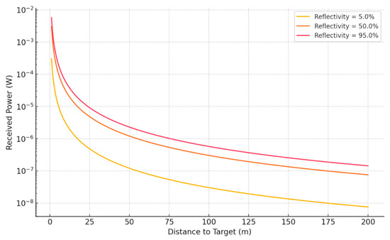
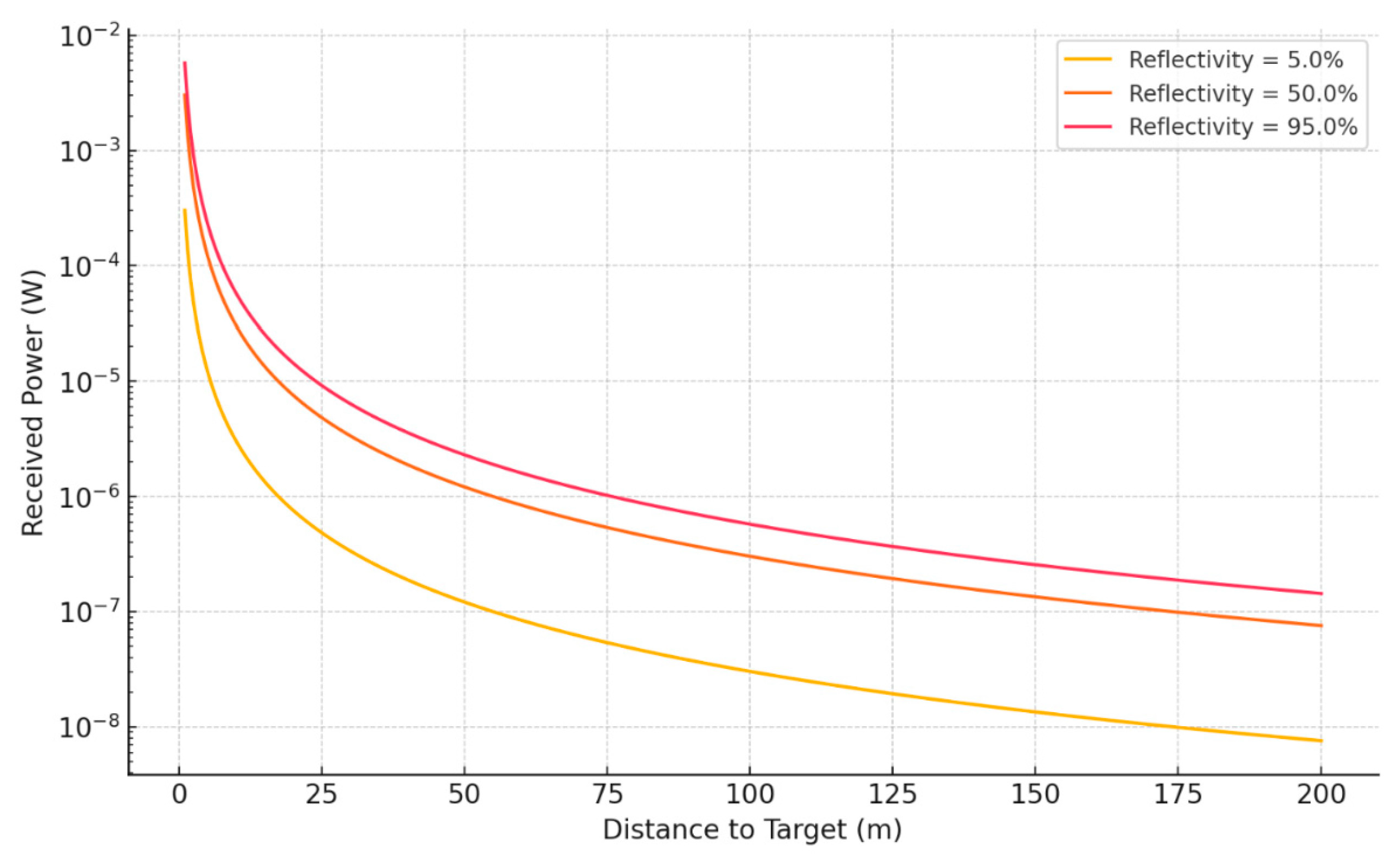
Figure 1 shows the received optical power obtained from Equation (1) for target reflectivities of 5%, 50% and 95% and ranges up to 200 m.
Figure 1.
Received optical power as a function of target range for 5%, 50%, and 95% target reflectivities.
Over these ranges and three different reflectivities, the received peak power varies from 7.6 nW to 5.7 mW, i.e., by almost six orders of magnitude. This wide dynamic range in the echo signal intensity is the origin of the walk error.
To characterize the walk error, the output signal of the cascaded transimpedance amplifier (TIA) and voltage amplifier within the LiDAR receiver can be modeled using a Gaussian pulse profile, expressed as
where A denotes the peak signal amplitude, t is the time in nanoseconds, and σ represents the standard deviation of the pulse, which is directly related to its pulse width.
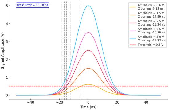
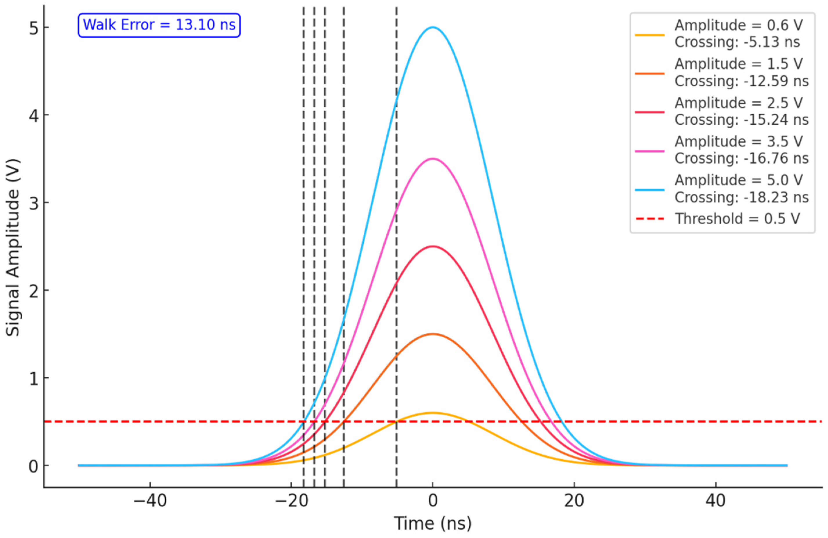
Based on this mathematical model, Figure 2 illustrates the impact of signal amplitude variations on the threshold crossing times. Because a fixed detection threshold is employed, fluctuations in the peak amplitude—which varies between 0.6 V and 5 V in this analysis—introduce an amplitude-dependent time shift.
Figure 2.
Threshold crossing time shifts (walk error) for varying signal amplitudes. The black dashed lines mark the threshold-crossing instants of the pulses. The time difference between the earliest and latest crossing times defines the walk error.
The standard deviation of the pulse, σ, is mathematically related to its full-width at half-maximum (FWHM) by the following expression:
In this analysis, the FWHM is chosen as 20 ns, which corresponds to a standard deviation of approximately 8.49 ns. To determine the threshold crossing time for the rising edge (tth), the Gaussian pulse equation is evaluated at the comparator threshold level, solving V(t) = Vth. This yields the analytical expression for the timing trigger:
where the threshold voltage Vth is set to 0.5 V for the walk error demonstration in Figure 2, and A represents the variable peak signal amplitude.
The maximum walk error (twalk) is defined as the maximum difference in threshold crossing times between the received signals with the lowest (Alow) and highest (Ahigh) amplitudes. Using the threshold crossing time derived previously, this maximum temporal shift can be analytically expressed as
Substituting the standard deviation of σ = 8.49 ns (derived from the 20 ns FWHM), a fixed threshold of Vth = 0.5 V, and the amplitude boundaries of Alow = 0.6 V and Ahigh = 5 V yield twalk = 13.1 ns, which matches the time shift illustrated in Figure 2.
A walk error of 13.1 ns corresponds to a range error of 196.5 cm and clearly has to be compensated. For pulse-width-based compensation, the relation between the echo amplitude and the width of the comparator output is needed.
A receiver in which an avalanche photodiode (APD) is followed by a TIA, a voltage amplifier and a comparator is considered. The comparator output, referred to below as the digital echo, starts at the rising threshold crossing and ends at the falling one, so its width PW is the difference between the two crossing times. Substituting Equation (4) for both crossings gives
where PW is the width of the digital echo for a peak amplitude A. The width grows with the amplitude through the logarithmic term, so a stronger echo produces a wider digital pulse; this monotonic relation is what the compensation exploits.
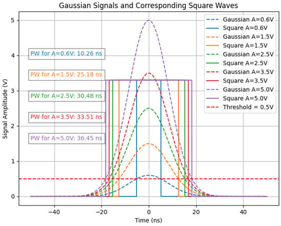
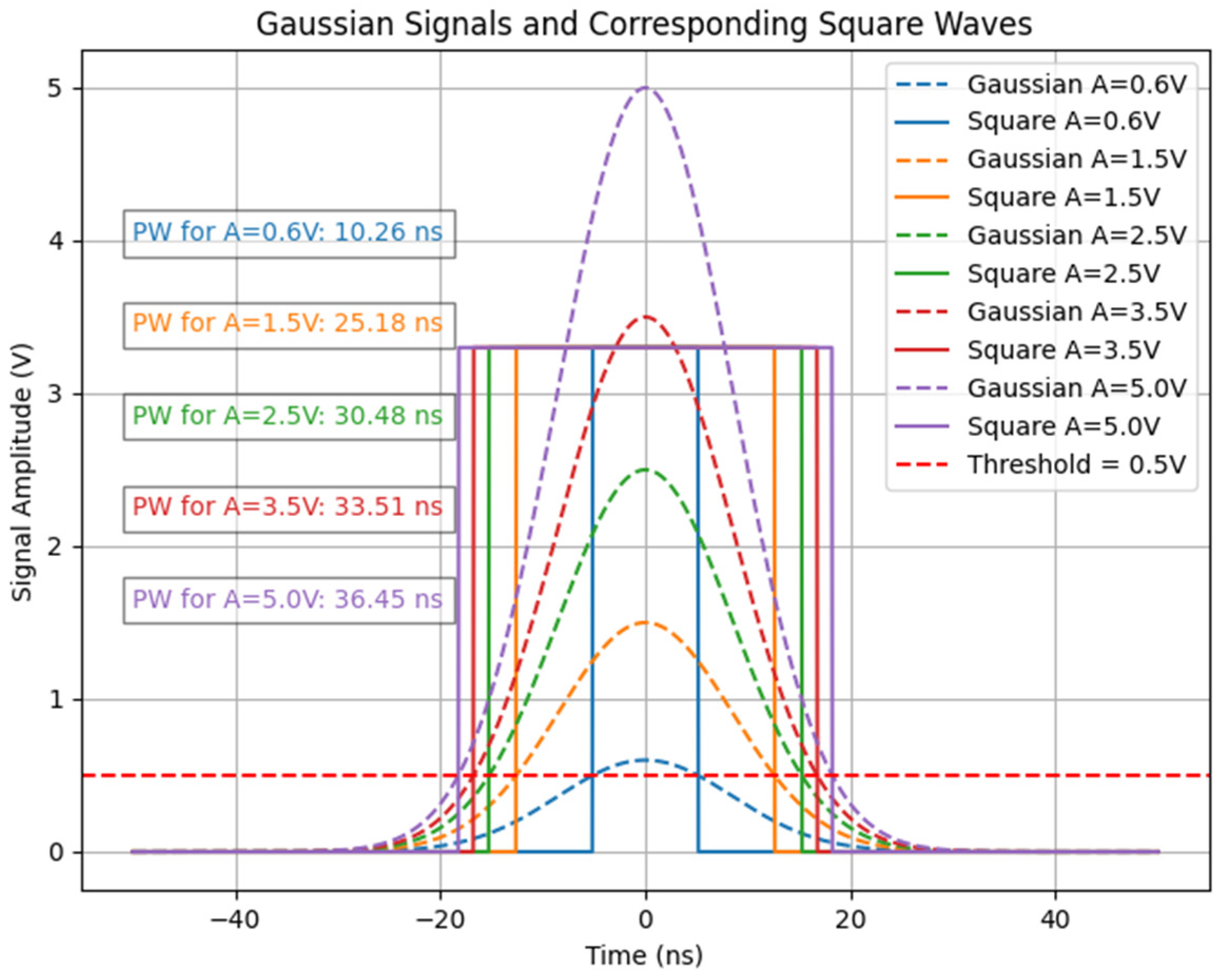
Figure 3 illustrates this behavior for a fixed threshold of 0.5 V and an FWHM of 20 ns; the Gaussian waveforms represent the analog echo at the comparator input.
Figure 3.
Illustration of the pulse width variation in the echo signals for different signal amplitudes.
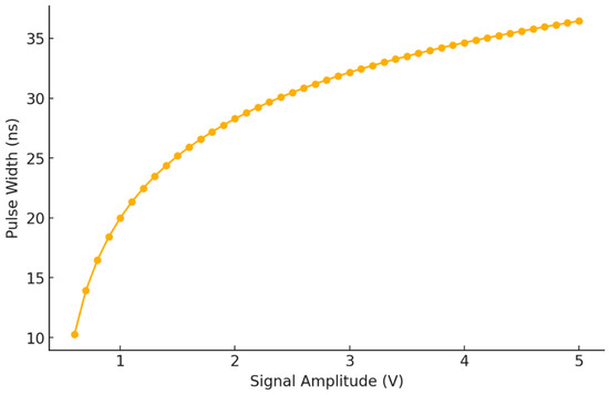
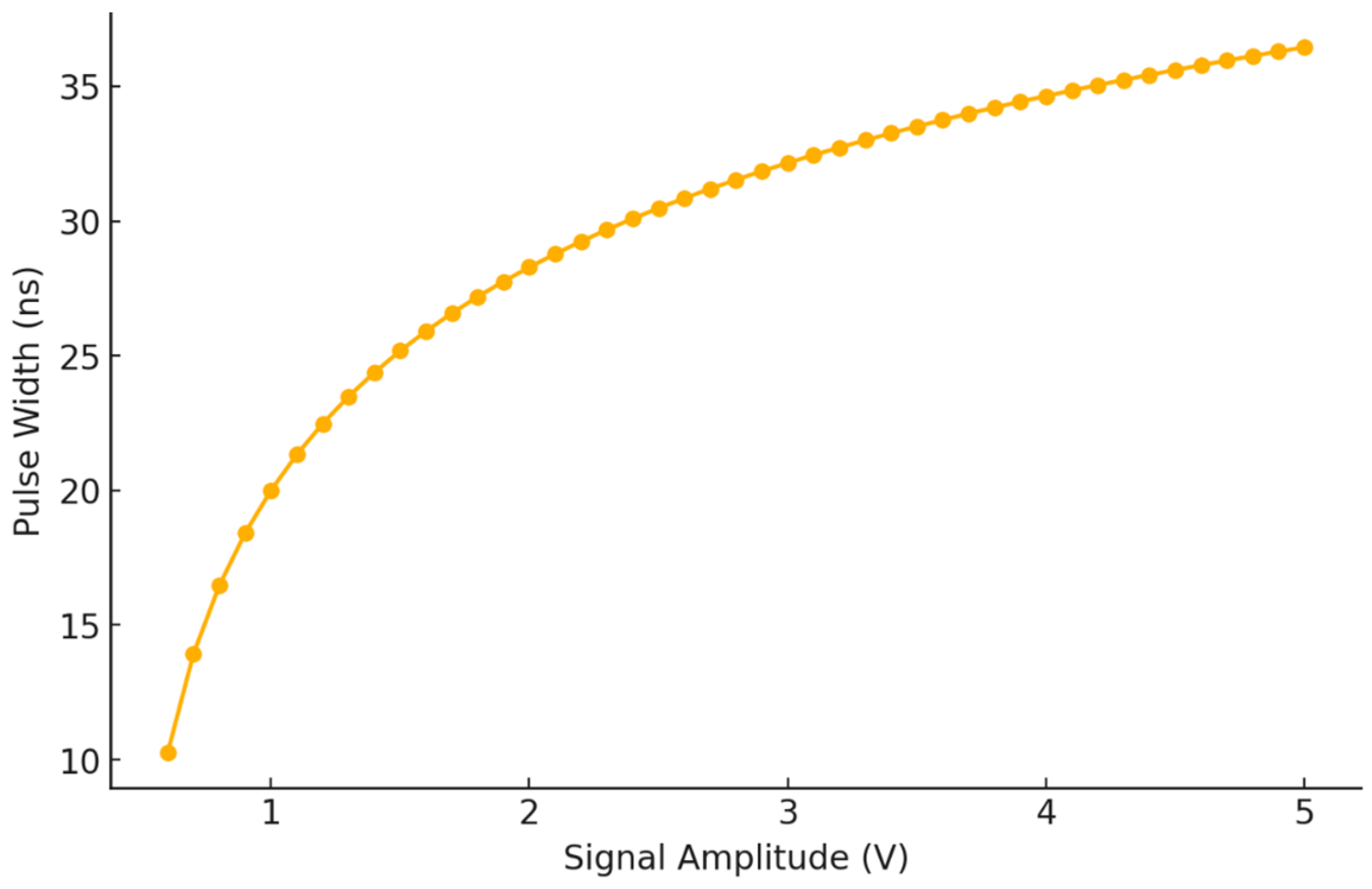
For echo amplitudes of 0.6, 1.5, 2.5, 3.5 and 5 V, the widths of the digital echo are 10.26, 25.18, 30.48, 33.51 and 36.45 ns, respectively. Figure 4 shows the complete relation obtained from Equation (6) for amplitudes between 0.6 V and 5 V. The width grows monotonically and most steeply at low amplitudes. The results indicate a highly predictable trend that can be accurately modeled using a polynomial equation. This predictable behavior shows that the pulse width of the generated digital echo signal can be effectively utilized to relate the signal intensity to the corresponding ToF error for walk error compensation.
Figure 4.
Pulse width versus signal amplitude based on Equation (6).
Walk Error Simulations
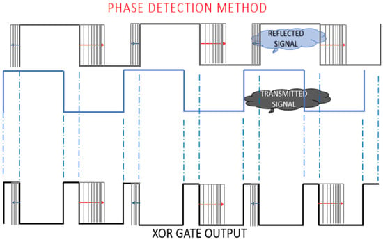
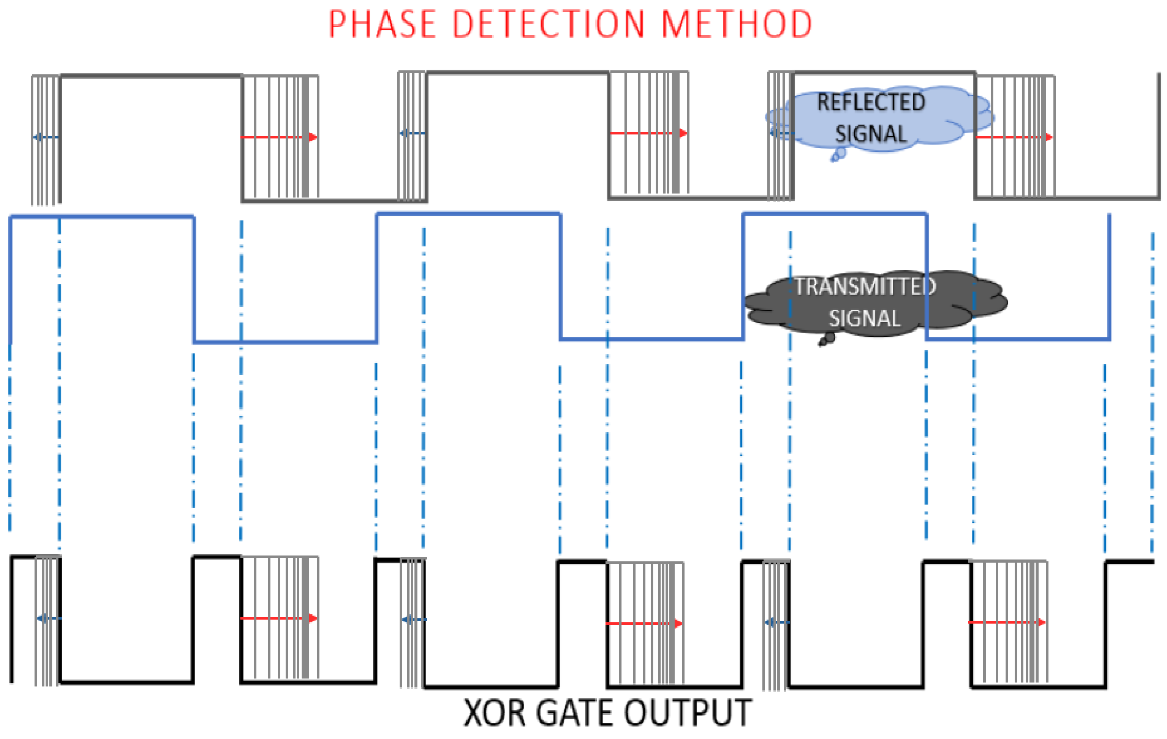
The phase detector of the TAC in [12] is a LUT-based XOR gate in an XC7A100T-1CSG324C FPGA (AMD, Santa Clara, CA, USA). Two properties of this detector limit its use in pulsed LiDAR. First, when the transmitted pulse width is shorter than the delay between the transmitted and received pulses, the two XOR inputs no longer overlap, and the output no longer depends on the delay, as illustrated in Figure 5, which restricts the usable pulse width and the depth measurement resolution.
Figure 5.
Effect of reflected light intensity variations on FPGA XOR gate-based phase detection. Gray lines mark the possible positions of the reflected signal edges, and the blue and red arrows show how the rising and falling edges shift as the intensity increases, changing the XOR output pulse width.
The second limitation is that the XOR output depends on both edges of both inputs. A stronger echo shifts the rising edge of the digital echo earlier, which shortens the XOR output pulse, and at the same time delays its falling edge, which lengthens it, as shown in Figure 5. Consequently, the rising edge leads to a reduction in the XOR gate’s output pulse width, whereas the falling edge causes an increase. These edge timing variations ultimately introduce significant errors into the iToF measurement.
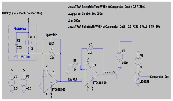
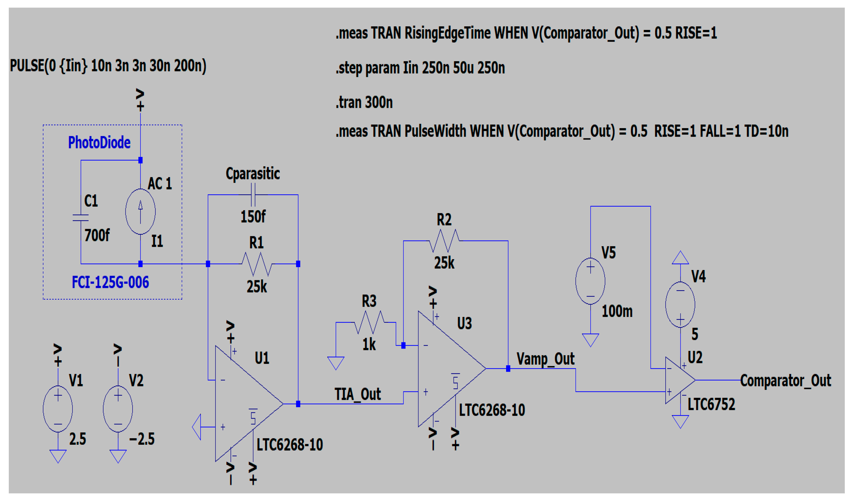
To examine in detail how pulse width expansion distorts the XOR-based TOF measurement, a LiDAR receiver circuit is designed as shown in Figure 6. Circuit simulations are carried out in LTspice XVII using photodiode current amplitudes ranging from 250 nA to 50 µA in steps of 250 nA, which emulates the wide dynamic range of reflected signal intensities in practical LiDAR operations. The applied photodiode current pulse features a 3 ns rise and fall time, a 30 ns pulse width, and a 30 µs period.
Figure 6.
A LiDAR receiver circuit to simulate the walk error.
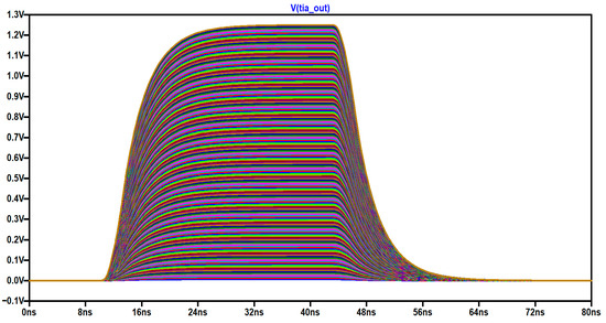
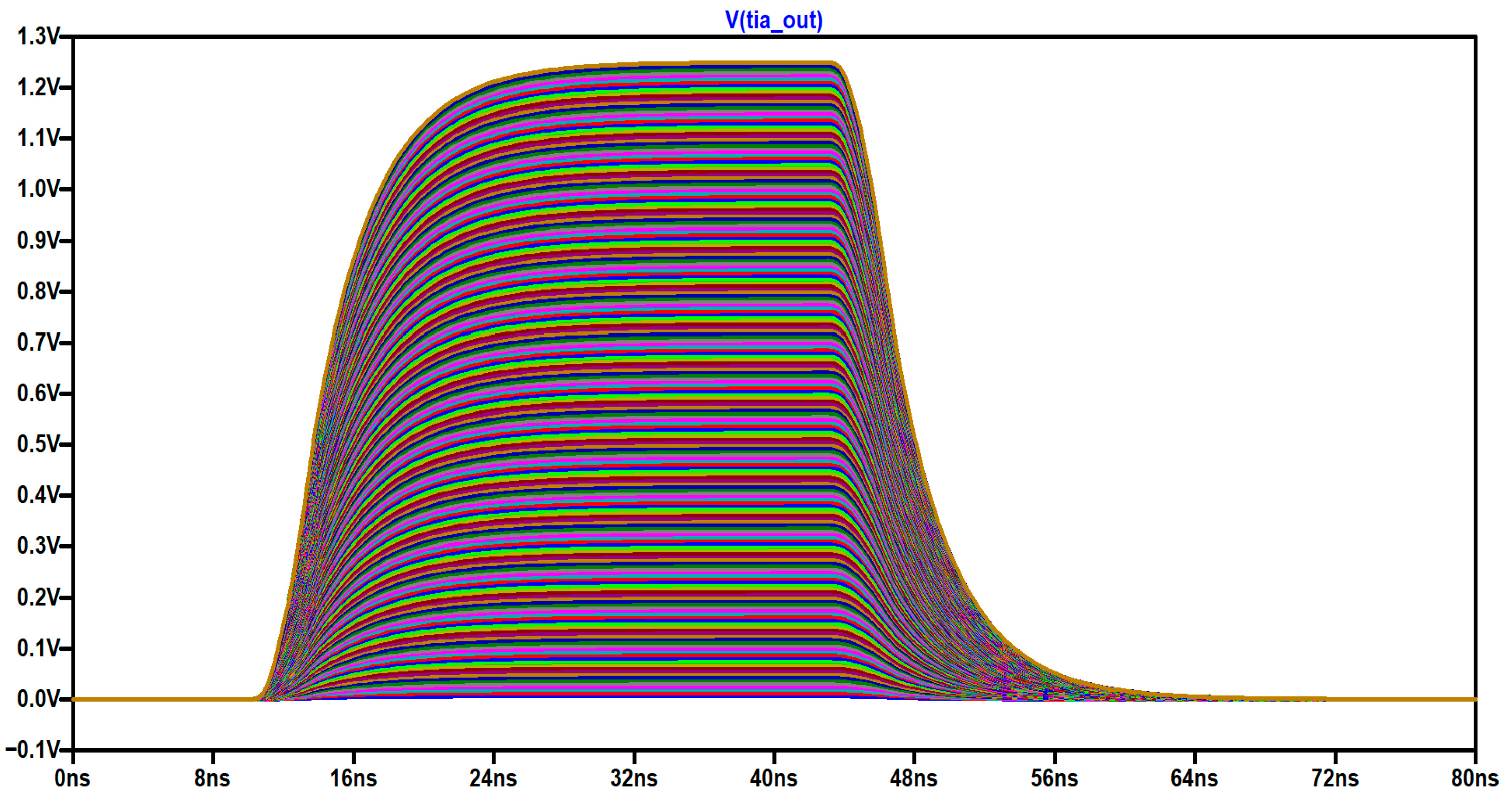
Initially, the photodiode current is converted into a voltage signal by a high-speed TIA stage. Featuring a gain of 25 kV/A, this TIA is implemented using the LTC6268-10 from Analog Devices, Inc. (Wilmington, MA, USA), which offers a unity-gain bandwidth of 4 GHz [37]. Figure 7 presents the simulated output signal of the TIA, confirming the target gain of 25 kV/A and illustrating that the TIA effectively responds to fast photodiode current pulses. Furthermore, because the op-amp operates with a 2.5 V positive supply voltage, output signal saturation is not observed.
Figure 7.
Output of the TIA for photodiode current amplitude values from 250 nA to 50 µA with 250 nA steps. The trace colors only distinguish individual simulation runs and carry no additional meaning.
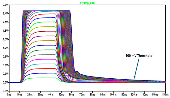
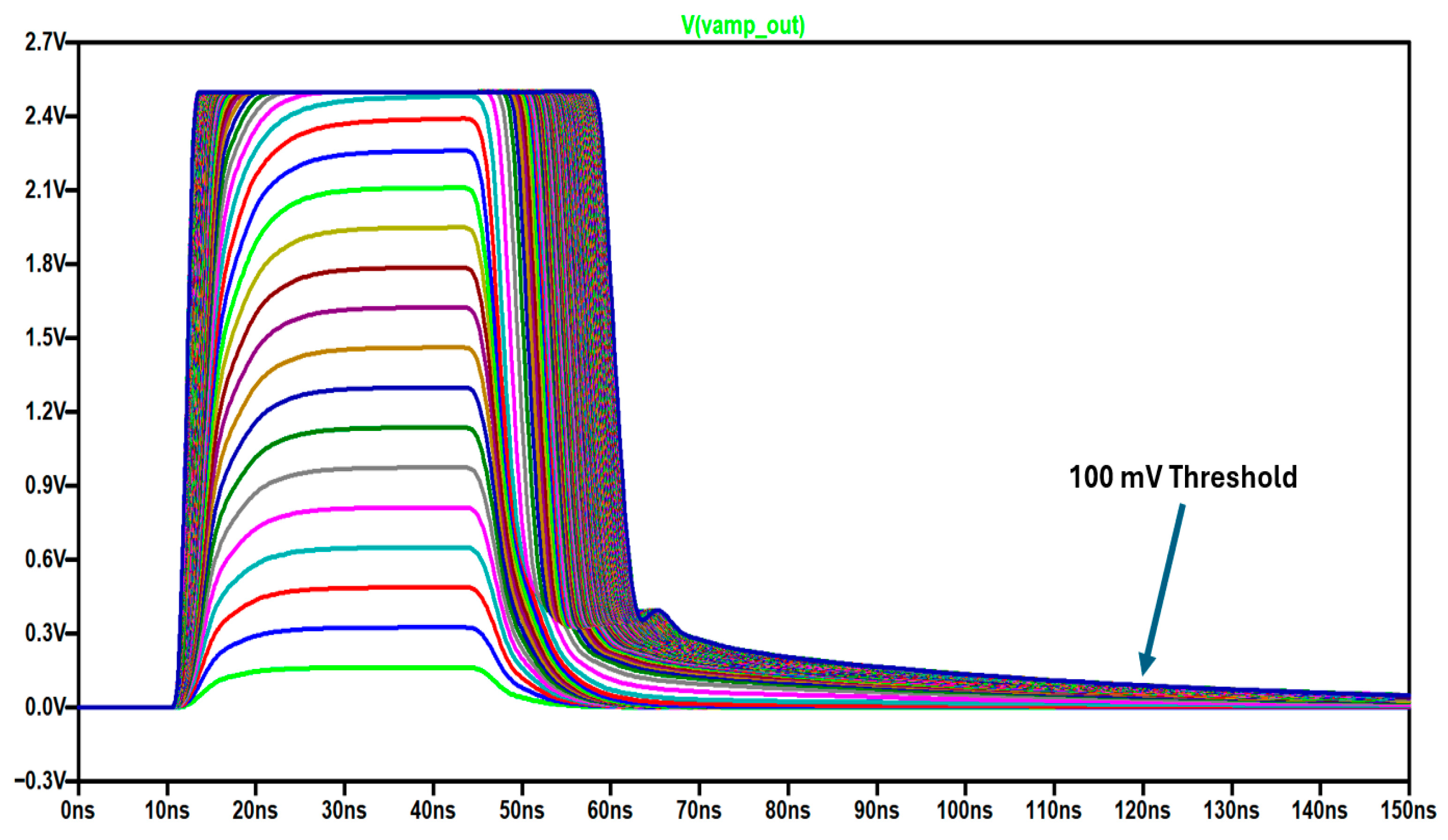
The second stage of the LiDAR receiver consists of a non-inverting voltage amplifier offering a gain of 26 V/V, also realized using the LTC6268-10. Combined with the preceding TIA, the receiver achieves a total transimpedance gain of 650 kV/A, which converts a 1 µA photodiode current into a 650 mV voltage signal. As shown in Figure 8, the amplifier clips signals exceeding the 2.5 V positive supply rail, flattening the top portion of the waveform. This pulse duration expansion is particularly pronounced along the falling edge.
Figure 8.
Output of the voltage amplifier for photodiode current amplitude values from 250 nA to 50 µA with 250 nA steps. The trace colors only distinguish individual simulation runs and carry no additional meaning.
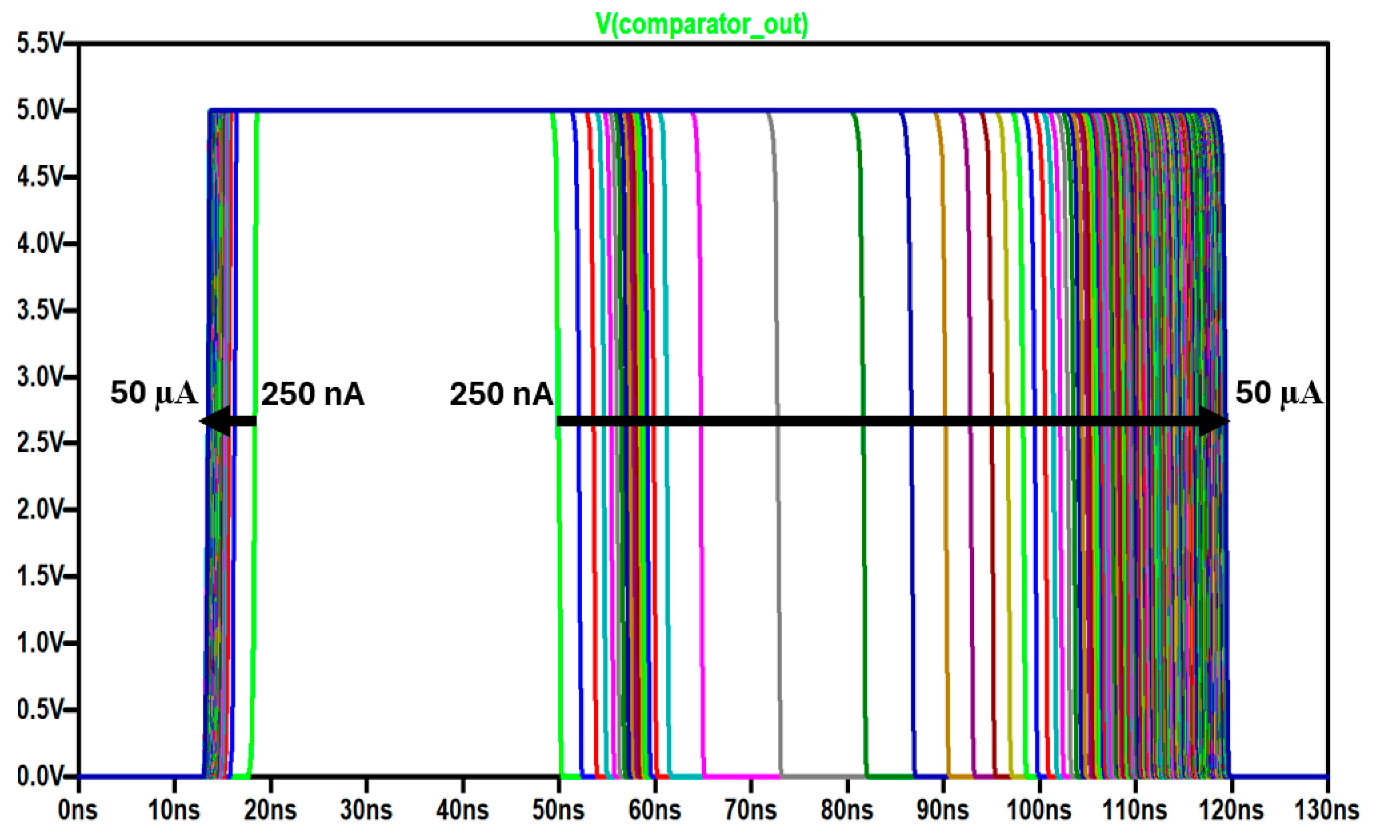
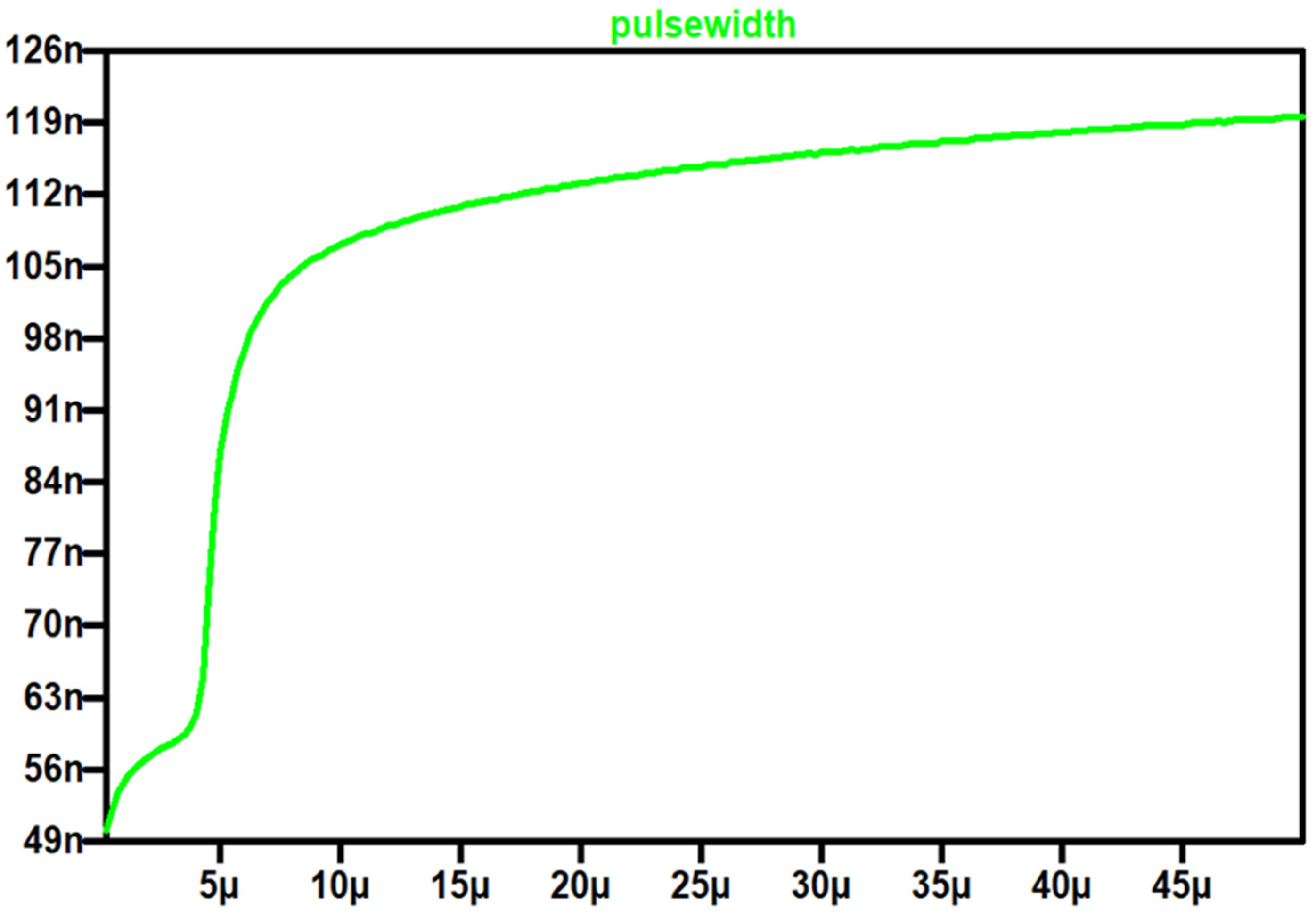
The final stage is a comparator implemented with the LTC6752 from Analog Devices, Inc. (Wilmington, MA, USA) [38]. Featuring a low propagation delay of approximately 2.9 ns and a toggle rate of up to 280 MHz, this high-speed comparator is well-suited for LiDAR applications. Figure 9 shows the resulting comparator output for photodiode current amplitudes ranging from 250 nA to 50 µA in 250 nA steps. These simulation results, as well as those in Figure 10 and Figure 11, are obtained using a 100 mV threshold voltage. As the photodiode current varies across this range, the pulse width expands substantially from approximately 49 ns to 119 ns, as observed in Figure 9.
Figure 9.
Output of the comparator for photodiode current amplitude values from 250 nA to 50 µA with 250 nA steps. The trace colors only distinguish individual simulation runs and carry no additional meaning.
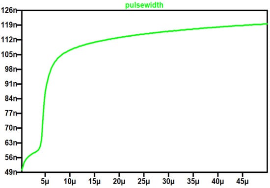
Figure 10.
Comparator output pulse width vs. photodiode current amplitude values from 250 nA to 50 µA with 250 nA steps.
Figure 11.
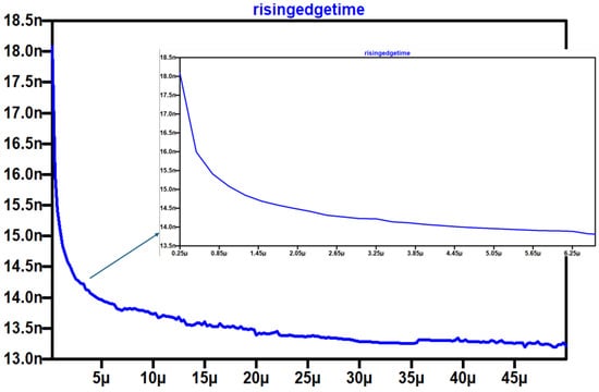
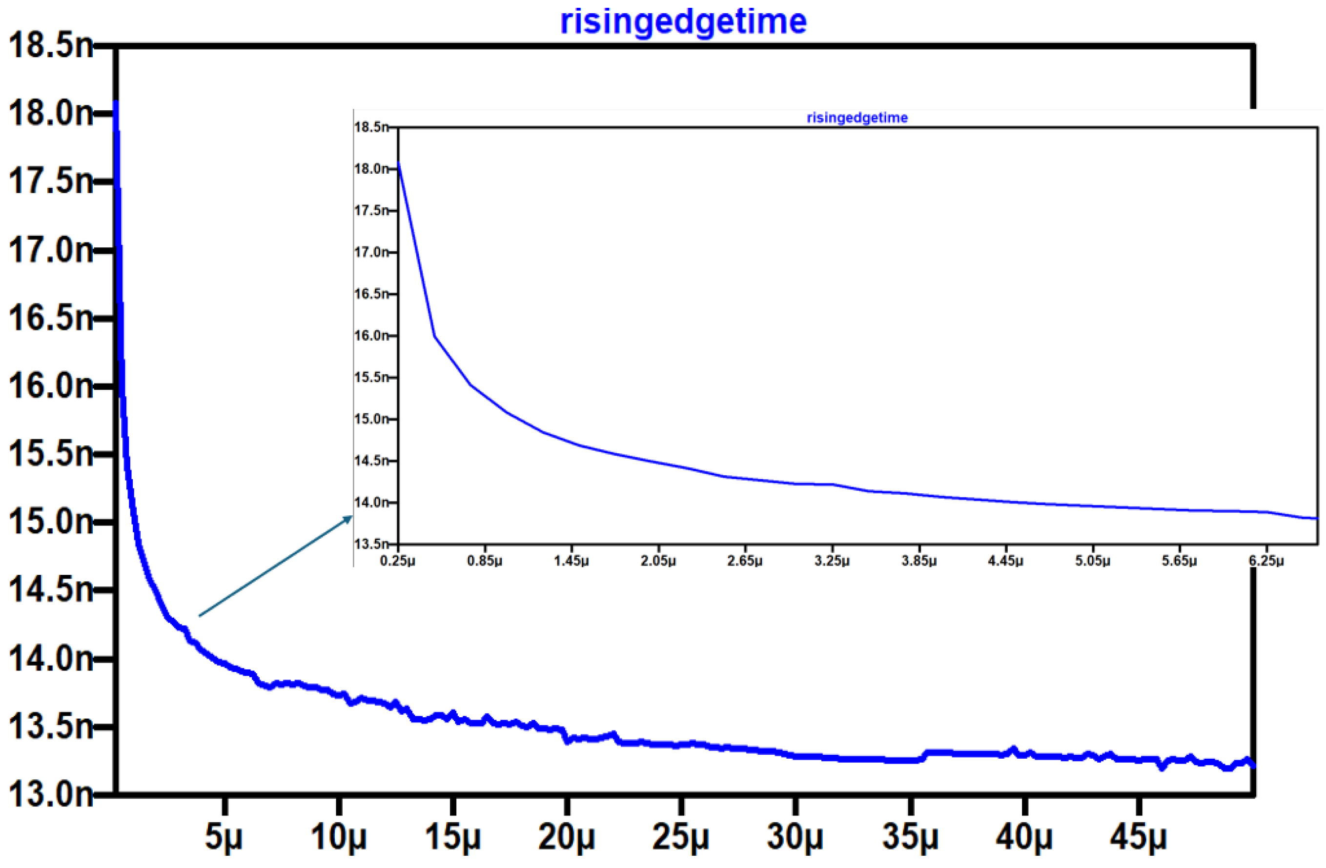
The walk error observed based on the arrival time of the rising edge of the comparator output for photodiode current amplitude values from 250 nA to 50 µA with 250 nA steps.
The pulse width expansion is noticeably more pronounced on the falling edge than on the rising edge, as shown in Figure 9. To examine the comparator output’s pulse width variation relative to the photodiode current in greater detail, a plot is obtained using the .meas TRAN PulseWidth command in LTspice, which is shown in Figure 10. For low photodiode currents (below approximately 5 µA), the pulse width increases steeply. At higher current levels (above ~15 µA), the rate of increase becomes more gradual, eventually reaching saturation when the photodiode current exceeds ~40 µA.
To quantify the walk error as a function of photodiode current, the arrival time—defined as the threshold-crossing point of the comparator output’s rising edge—is determined using the .meas TRAN RisingEdgeTime command in LTspice. The resulting plot is presented in Figure 11. For a 250 nA photodiode current, the rising edge of the output pulse occurs at 18.08 ns. As the current increases toward 6 µA, this arrival time drops sharply. A nearly linear decrease follows up to 35 µA, beyond which the timing shows minor fluctuations while remaining largely stable at approximately 13.26 ns. Consequently, as the photodiode current increases, the rising edge shifts earlier by 4.82 ns (from 18.08 ns down to 13.26 ns), introducing a 4.82 ns walk error. This 4.82 ns walk error translates to a substantial distance measurement error of approximately 72.3 cm.
The comparator threshold is a design parameter that affects both the minimum detectable echo signal power and the quality of the pulse-width information. The results in Figure 9, Figure 10 and Figure 11 were obtained with a 100 mV threshold, which corresponds to a minimum detectable photocurrent of 153.8 nA, or an optical power of 3.08 nW for an APD responsivity of 50 A/W and a total transimpedance gain of 650 kV/A. At this level, however, the threshold intersects the slowly decaying tail of the amplified echo shown in Figure 8, where the shallow slope makes the timing sensitive to noise, and the ringing at about 65 ns and 0.4 V adds further pulse-width fluctuations. Raising the threshold to 600 mV shifts the threshold-crossing point above both artifacts, at the cost of degrading sensitivity, which raises the minimum detectable photocurrent to 0.92 µA, corresponding to an optical power of 18.5 nW.
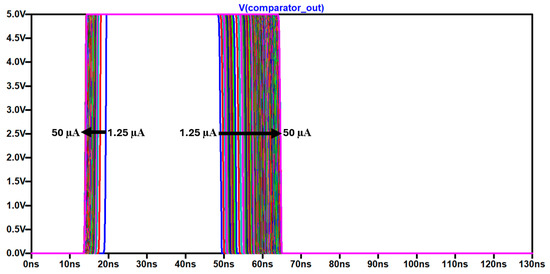
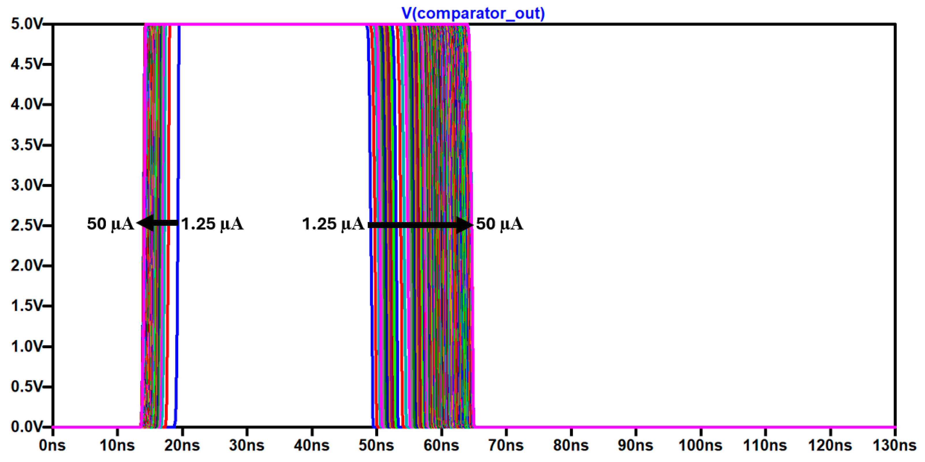
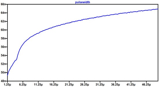
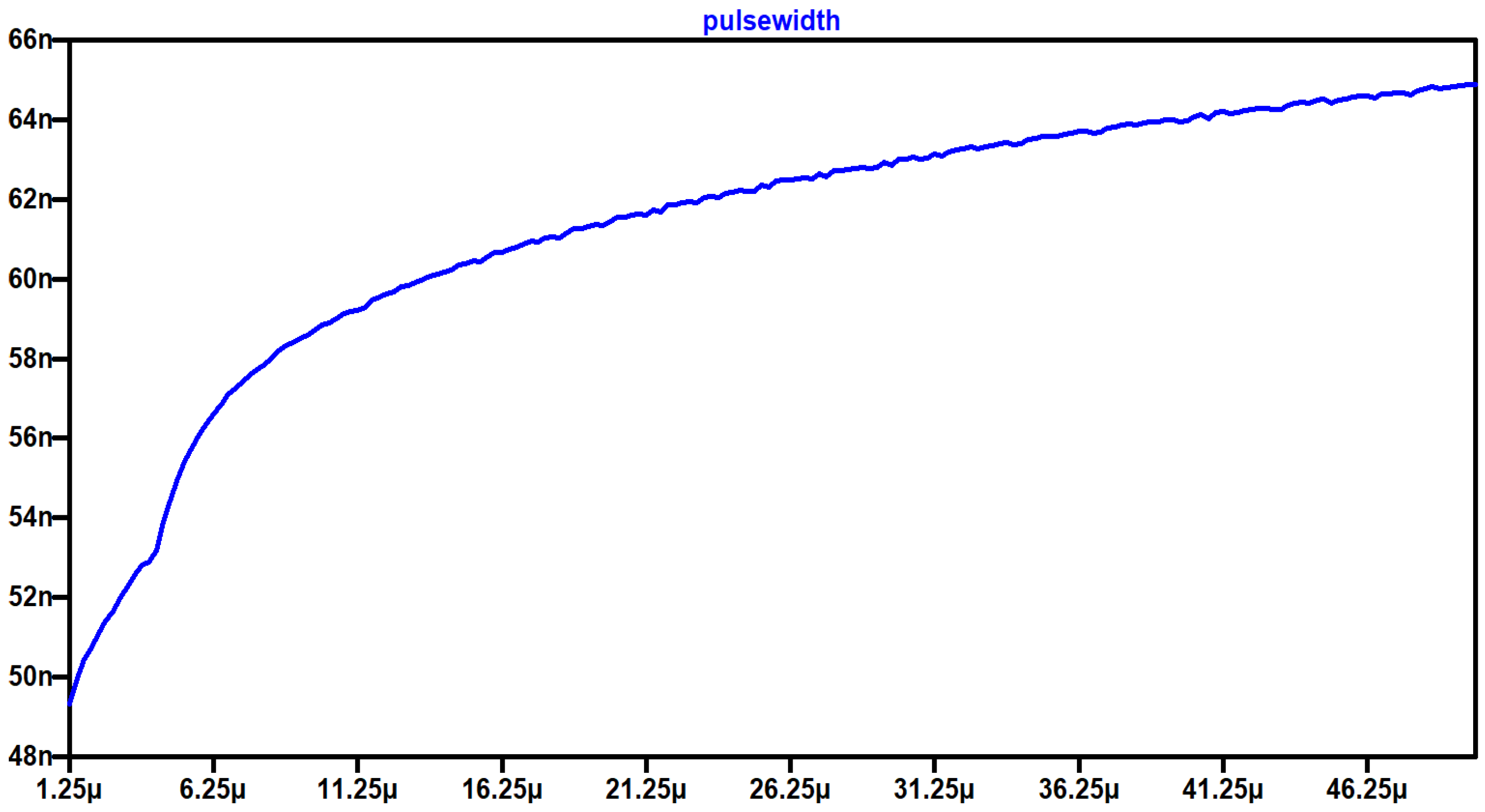
When the comparator threshold voltage is set to 600 mV, the output signal is shown in Figure 12, where the photodiode current varies from 1.25 µA to 50 µA in steps of 250 nA. Compared with the results in Figure 9 and Figure 10, the pulse width expansion decreases significantly and exhibits a more linear behavior. The detailed response of the pulse width relative to photodiode current variations is plotted in Figure 13. By increasing the threshold voltage to 600 mV, the maximum pulse width at 50 µA drops from approximately 119 ns to 65 ns, while the minimum pulse width remains largely unchanged at around 49 ns.
Figure 12.
Output of the comparator with a 600 mV threshold for photodiode current amplitudes from 1.25 µA to 50 µA in 250 nA steps. The trace colors only distinguish individual simulation runs and carry no additional meaning.
Figure 13.
Comparator output pulse width vs. photodiode current amplitude with a 600 mV threshold (1.25 µA to 50 µA; 250 nA steps).
Increasing the comparator threshold from 100 mV to 600 mV enhances the noise immunity of the pulse-width measurements and consequently improves the walk error compensation; however, it imposes an inherent trade-off on the maximum measurable range, which can be quantified using Equation (1). The 600 mV threshold raises the minimum detectable optical power by a factor of six (7.8 dB). Since the received power scales as 1/R2 in clear air, the threshold-limited maximum range decreases by a factor of √6 ≈ 2.45. Specifically, for the parameters of Figure 1, it drops from 314 m to 128 m for a 5% target reflectivity and from 991 m to 405 m for a 50% target reflectivity. The range values stated above represent upper bounds, as they neglect detector noise and detection probability; a noise-limited analysis would lower these limits for both thresholds. In addition, the span of echo widths that the pulse-width channel must resolve narrows from about 70 ns, ranging from 49 to 119 ns, to about 16 ns, ranging from 49 to 65 ns, ensuring that the width is no longer dictated by the noise-sensitive tail of the pulse. Consequently, the walk error correction becomes more robust and less susceptible to noise, though it remains valid only for the specific threshold at which it was calibrated; any adjustment to the threshold, therefore, requires a dedicated calibration curve.
In summary, a stronger echo shifts the rising edge of the digital echo earlier and delays its falling edge, and the XOR detector combines both effects in its output, leading to significant TOF measurement deviations. In the improved TAC, phase detection is, therefore, performed with a DFF that responds only to the rising edges of the transmitted pulse and the echo. The ToF measurement then contains only the leading-edge walk error, which is corrected using the echo pulse width measured in a separate channel. Because the DFF is set by an edge rather than by the overlap of two pulses, the transmitted pulse width can also be shorter than the ToF, which removes the minimum-pulse-width restriction of the XOR design. The implementation and the experimental results are described in Section 3.
3. Improved Two-Channel FPGA-Based TAC: Experimental LiDAR Setup and Results
This section describes the implementation of the improved two-channel TAC and its evaluation in a laboratory LiDAR setup. In operation, a trigger signal fires a short laser pulse and at the same time serves as the start reference of the TAC. The echo from the target is focused onto an APD, amplified and converted into a digital echo by a comparator. The TAC measures the phase shift between the trigger and the digital echo, from which the distance is obtained.
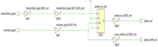
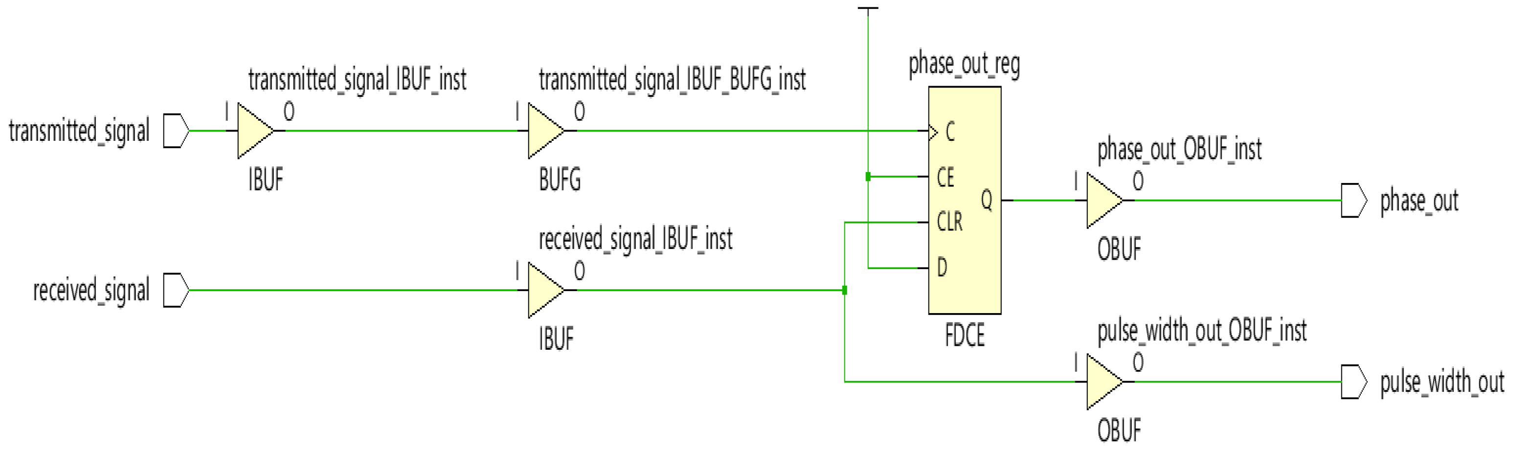
The digital processing for the phase shift measurement is implemented within a low-cost AMD XC7A100T-1CSG324C FPGA IC. Its schematic, obtained from the implementation results in Vivado Design Suite 2019.2, is shown in Figure 14. To measure the phase shift between the transmitted and reflected signals, a DFF instantiated via the FDCE primitive is utilized. As noted earlier, replacing the XOR-gate design from [12] with this DFF architecture is implemented primarily to mitigate walk error. Initially, the phase_out signal is at logic low. When a rising edge transition occurs on the transmitted signal connected to input C, it triggers the DFF, transferring the logic high level at input D to output Q, which corresponds to the phase_out signal. Subsequently, when the rising edge of the received signal arrives at the asynchronous clear input CLR, output Q is asynchronously reset to logic zero. Consequently, a digital signal with a pulse width equal to the phase shift between the transmitted and reflected signals is generated. The period of this generated signal matches that of the transmitted and reflected signals, while its pulse width represents the accurate TOF of light through air plus the system’s offset propagation delay. Only one FDCE primitive is required per ToF channel.
Figure 14.
The schematic of the digital phase detection part of the FPGA-based TAC.
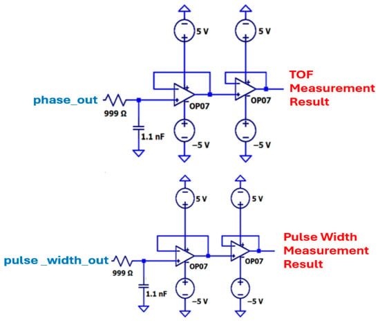
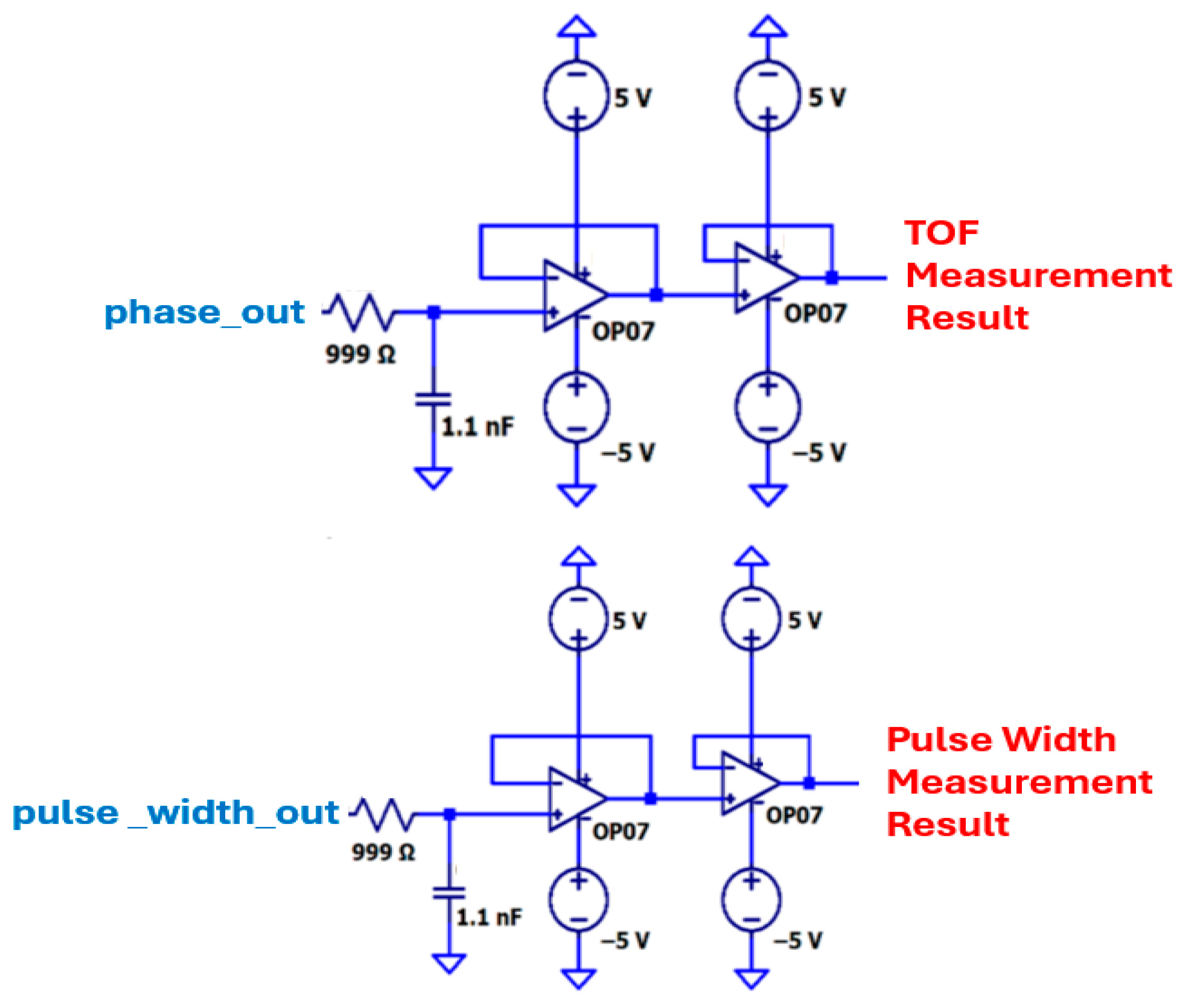
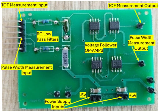
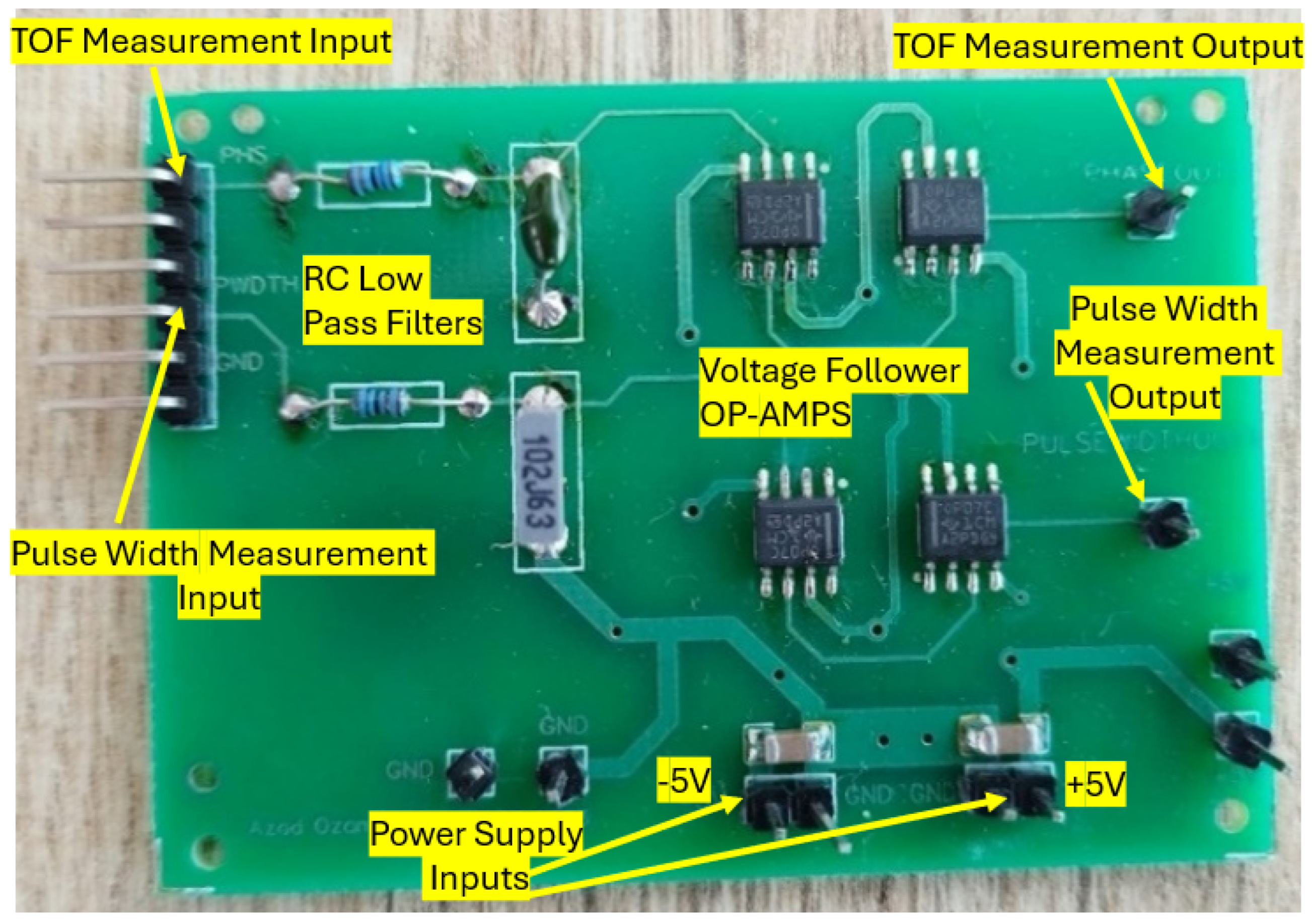
The two-channel analog circuit representing the discrete analog circuitry of the TAC is presented in Figure 15, and the fabricated PCB for this setup is shown in Figure 16. This low-complexity, cost-effective circuit converts the pulse width of the digital input signal into an analog DC output voltage. Consequently, both the TOF and the reflected signal’s pulse width are measured simultaneously, allowing the pulse width information to be utilized for walk error compensation. The circuit architecture for each channel comprises a first-order low-pass filter followed by a buffer stage with voltage-follower op-amps. Further details regarding the foundational operating principle and experimental evaluation of this topology are provided in [12]. In this work, a second channel is introduced specifically for pulse width measurement, and the total number of voltage-follower op-amps is reduced from three to two. Two voltage followers are found to be sufficient to achieve a TAC output with low noise and ripple. Apart from the second channel and the omitted third follower, the conversion chain is identical to that of [12], where it is characterized between 3 °C and 93 °C and across supply voltages from ±3.5 V to ±10 V, as discussed in Section 4.2.
Figure 15.
The schematic of the analog part of the FPGA-based TAC.
Figure 16.
Fabricated PCB for the analog part of the FPGA-based TAC.
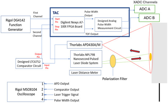
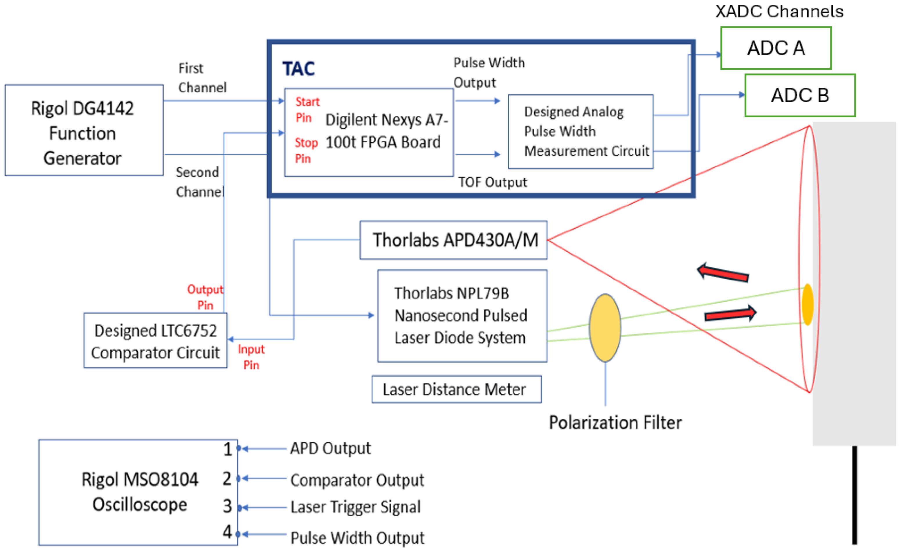
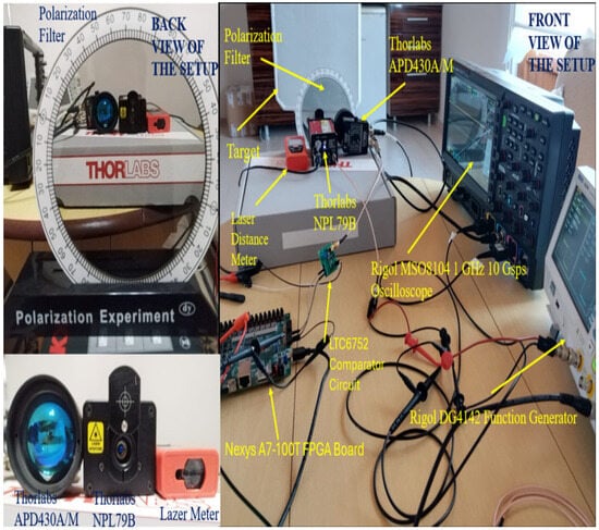
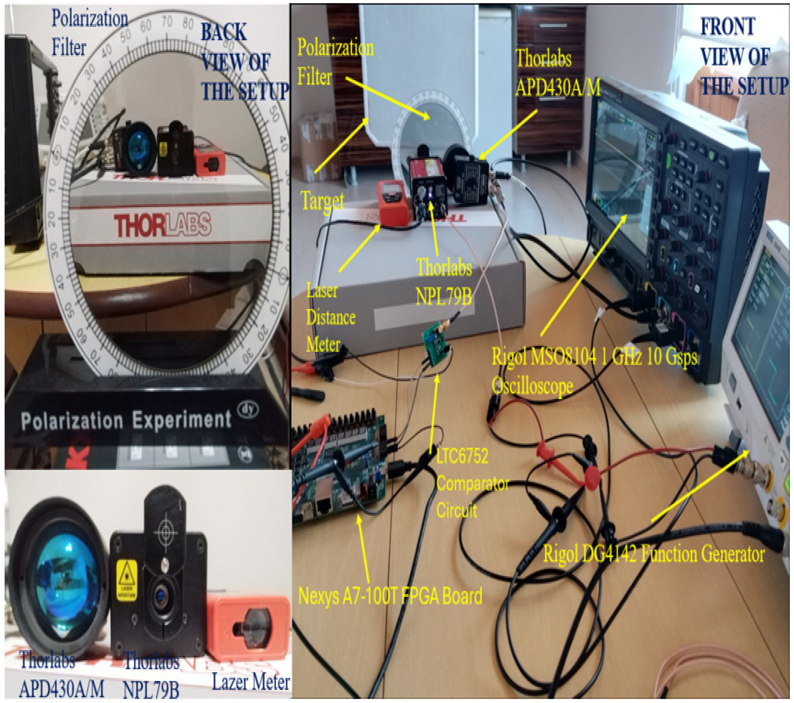
An overview of the experimental setup is presented in Figure 17, while Figure 18 shows the front and back views of the physical LiDAR system. The setup operates as follows: a DG4142 function generator (RIGOL Technologies, Suzhou, China) produces two identical pulse signals, each with a 360 ns period and a 20% duty cycle. The first channel delivers the start reference signal to the Nexys A7-100T FPGA board (Digilent, Pullman, WA, USA), connecting directly to the clock input of the DFF as shown in Figure 14 to initiate phase shift detection for iToF measurement. The second channel drives the trigger input of a NPL79B nanosecond pulsed laser (Thorlabs Inc., Newton, NJ, USA) with a wavelength of 785 nm and a peak power of 88 mW to emit optical ranging pulses. These pulses pass through a rotatable polarization filter, which gradually attenuates the light intensity to simulate a range of target reflectivities.
Figure 17.
The overall architecture of the LiDAR experimental setup.
Figure 18.
Overview of the LiDAR experimental setup and instrumentation.
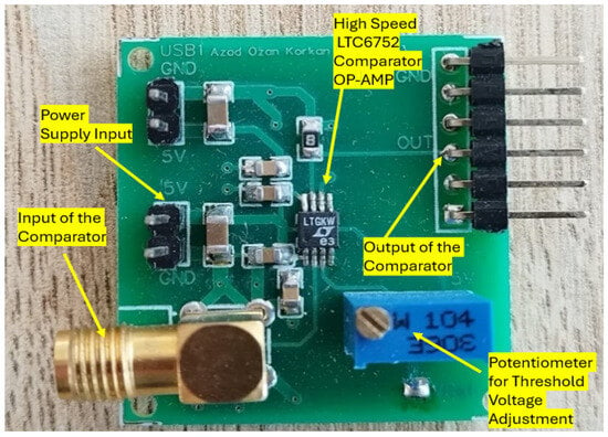
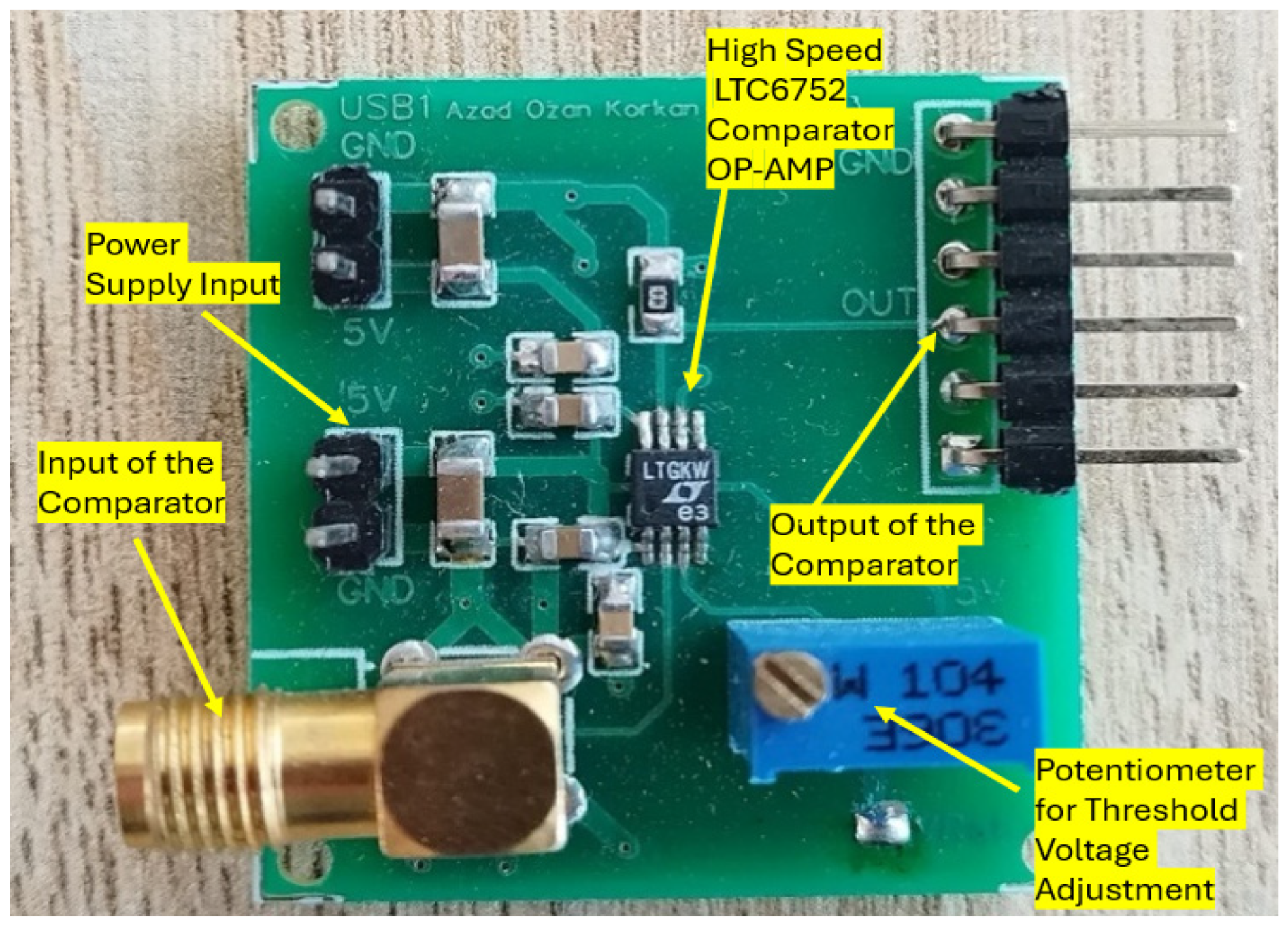
Once reflected off the target, the returning optical echo is focused onto a APD430A/M Si variable-gain APD module (Thorlabs Inc., Newton, NJ, USA) via a focusing lens to convert the optical signal into an analog voltage. The output of this APD module connects to a comparator circuit, which converts the analog voltage into a digital pulse. The comparator circuit is implemented using an LTC6752 high-speed comparator (Analog Devices Inc., Wilmington, MA, USA) IC featuring a propagation delay of approximately 2.9 ns, and its fabricated PCB is shown in Figure 19. Although the threshold voltage can be adjusted via an onboard potentiometer, it is maintained at a constant 0.259 V throughout the experiments.
Figure 19.
Fabricated PCB of the LTC6752 comparator circuitry.
During threshold detection, the propagation delay of the comparator inherently varies with signal amplitude due to input overdrive dispersion. Combined with slew-rate fluctuations driven by varying optical intensities, this behavior directly induces timing walk error. The output of the comparator circuit connects to the stop pin on the FPGA board, representing the received signal. This signal serves as the reset trigger for the internal DFF inside the FPGA chip to perform phase-based iToF measurement. To capture the system dynamics, a MSO8104 oscilloscope (RIGOL Technologies, Suzhou, China) with a 1 GHz bandwidth and 10 GS/s sampling rate is employed to monitor four key signals: the APD430A/M output, the comparator output, the laser trigger signal, and the FPGA’s internal DFF output.
Two distinct output signals are generated by the FPGA board, consisting of the pulse-width signal, which directly routes the received echo pulse from input to output, and the iToF signal, corresponding to the output of the internal DFF. These signals feed into the two parallel processing channels shown in Figure 15 and Figure 16. Specifically, the first channel, designated as phase_out, converts the iToF phase information from the DFF output into a proportional DC voltage. The second channel converts the pulse width of the reflected signal into an analog DC level dedicated to walk error compensation. To perform simultaneous measurements, the outputs of these two circuits connect to the ADC A and ADC B channels of the internal 12-bit XADC block. The digitized results are subsequently transferred to PC-based Python software (version 3.7.2) for further analysis. Under this configuration, given a 360 ns laser trigger period, a 1 ns phase shift translates into an approximate voltage change of 9.5 mV. The ADC B and ADC A inputs capture the pulse width for walk error compensation and the iToF data, respectively. Finally, a Python-based algorithm applies polynomial fitting to these parameters to effectively mitigate walk error and yield high-accuracy distance measurements. The XADC has a resolution of 12 bits over a 1 V input range, i.e., 0.244 mV per LSB, which corresponds to a timing resolution of about 26 ps and a range resolution of 3.9 mm at a conversion gain of 9.5 mV/ns.
With the laser diode running continuously at the 360 ns period as given before, the RC low-pass filter (999 Ω, 1.1 nF, and τ = 1.099 µs) and the two voltage followers average the DFF output over many laser pulses. Therefore, every sample of the TAC output represents the mean of the preceding pulses rather than a single-shot value. Even for an abrupt change of 50 ns in the measured interval, the output settles to 99.5% within 25 µs, which corresponds to 69 laser pulses. This settling time limits the rate of independent readings to 40 kHz. The two XADC channels are read in continuous channel-sequencer mode at 500 kilosamples per second (kSPS) each, which gives one raw reading per channel every 2 µs. Each reported ToF and pulse-width value is the mean of 16 consecutive samples. These samples cover an acquisition window of 32 µs, or about 90 laser pulses, and are taken after a settling time of 25 µs. Including this interval, one measurement takes 57 µs, or about 158 laser pulses, and the effective measurement rate is 17.54 kHz. .
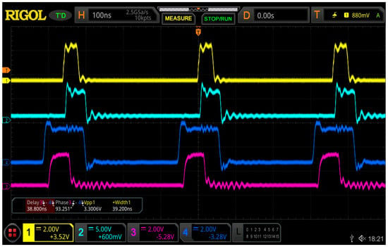
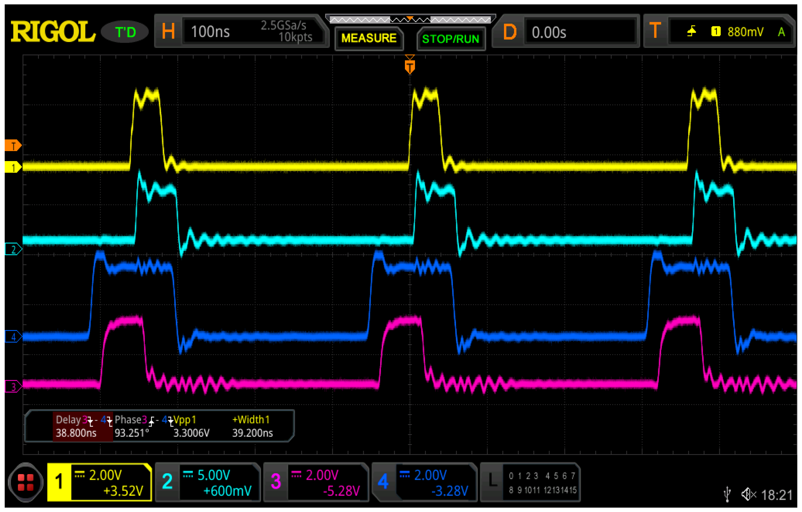
Oscilloscope traces capturing the four primary signals of the experimental setup are presented in Figure 20. The top trace, shown in orange, represents the output of the Thorlabs APD430A/M amplified APD module. The light blue trace corresponds to the output of the comparator circuit, whereas the dark blue trace denotes the transmitted signal provided by Channel 1 of the signal generator, accompanied by a phase-aligned replica from Channel 2. This signal triggers the DFF to initiate phase detection. The bottom trace, shown in pink, shows the DFF output, where its rising edge is triggered by the transmitted signal and its falling edge by the comparator output. Consequently, the pulse width of this signal directly represents the ToF interval between transmission and reception. This pulse width is subsequently converted into an analog DC voltage using the circuit shown in Figure 15, where the resulting amplitude determines the distance.
Figure 20.
Captured oscilloscope waveforms of the experimental setup: APD output (orange), comparator output (light blue), transmitted trigger signal (dark blue), and DFF output (pink).
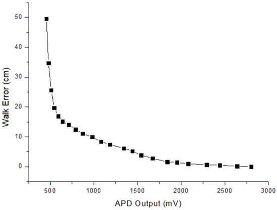
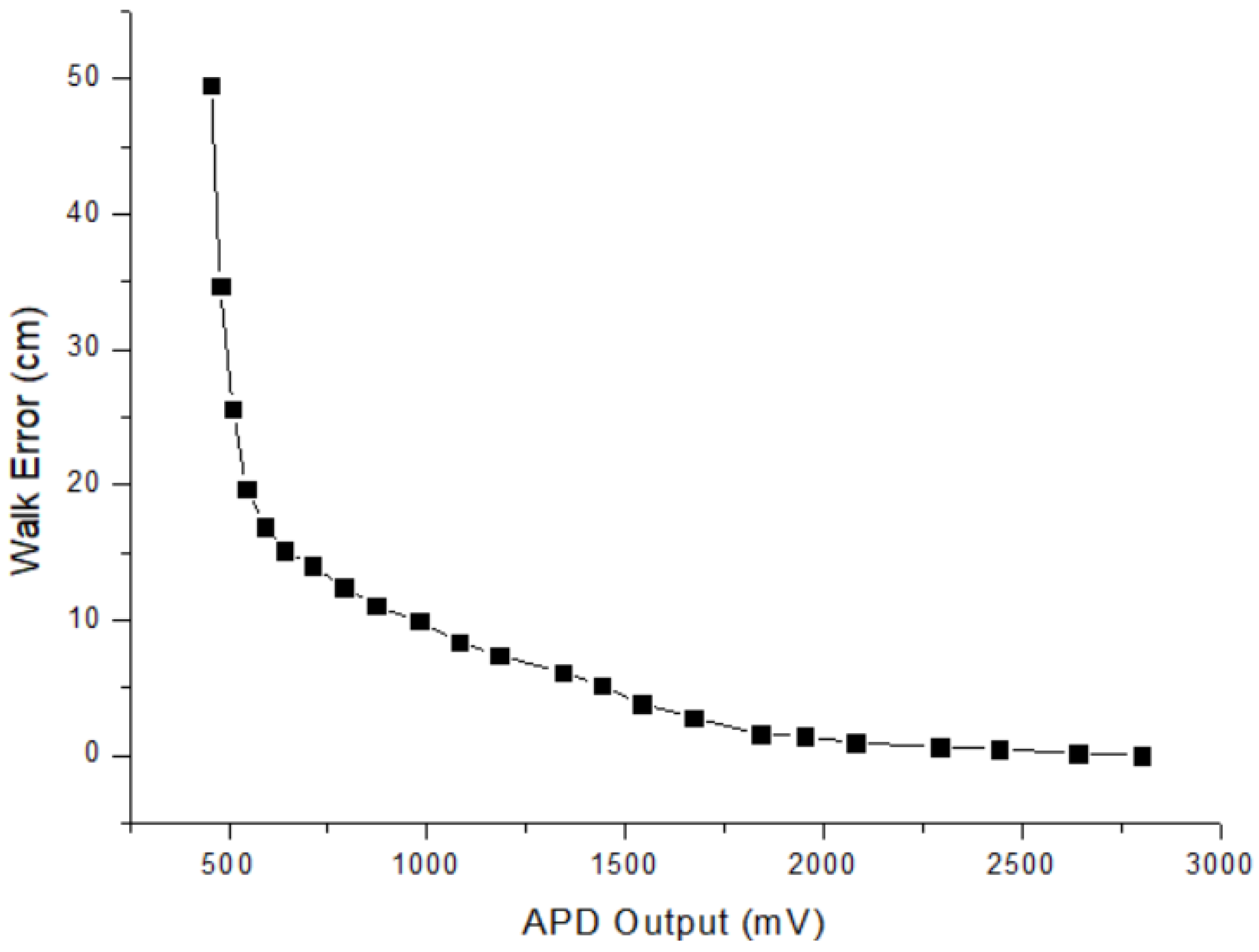
The walk error is evaluated by rotating the polarization filter, which gradually attenuates the returning optical power while keeping the target at a constant distance. Figure 21 illustrates this walk error plotted against the signal amplitude coming from the Thorlabs APD430A/M module. As the optical echo weakens and the APD output voltage drops, the measured distance starts to drift, with this deviation becoming much larger at low light intensities. More specifically, these results show that a dark target with low reflectivity, such as a black surface, can appear 49.5 cm farther away than a highly reflective white target at the exact same physical position.
Figure 21.
Characterization of uncompensated walk error as a function of received APD signal amplitude.
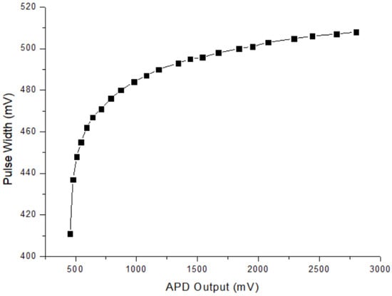
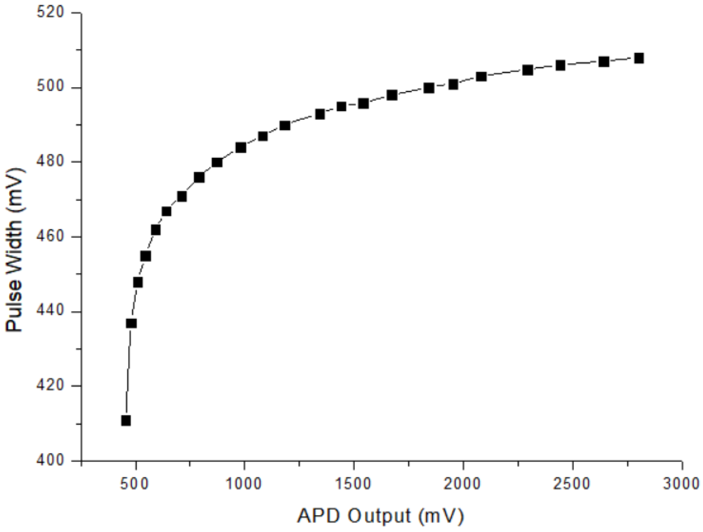
The proposed compensation method uses the relationship between pulse width and walk error to correct the measurement drift. First, an experiment is carried out using the polarization filter setup to measure the echo pulse width as a function of the Thorlabs APD output amplitude, as shown in Figure 22. Higher reflected light intensity leads to a wider pulse width, which agrees well with the analytical and simulation results discussed in Section 2.
Figure 22.
Measured echo signal pulse width as a function of the Thorlabs APD output amplitude.
Figure 23 shows the walk error as a function of the measured echo pulse width. Because the TAC outputs the pulse width as a voltage, the horizontal axis is in millivolts; 9.5 mV corresponds to 1 ns. The digital averaging does not add to the averaging performed by the converter itself. Its purpose is to suppress the quantization and noise of the readout, so that the remaining error is set by the noise, ripple and drift of the analog outputs. For the calibration points of Figure 23, 1024 samples are averaged per measurement point, which corresponds to 2.048 ms or about 5689 laser pulses. With this averaging, the readout noise is negligible against the residual of the polynomial fit.The measured curve has an average slope of about 5 cm/ns and it is clearly nonlinear. Therefore, an empirical calibration curve is used, as in previous pulse-width compensation methods. A seventh-order polynomial is fitted to the calibration points using least-squares. The coefficient of determination is R2 = 0.998, the RMS residual is 0.5 cm and the largest residual is 0.9 cm, which is small compared with the 42 cm of uncompensated walk error.
Figure 23.
Measured walk error as a function of echo signal pulse width and the corresponding polynomial fitted curve.
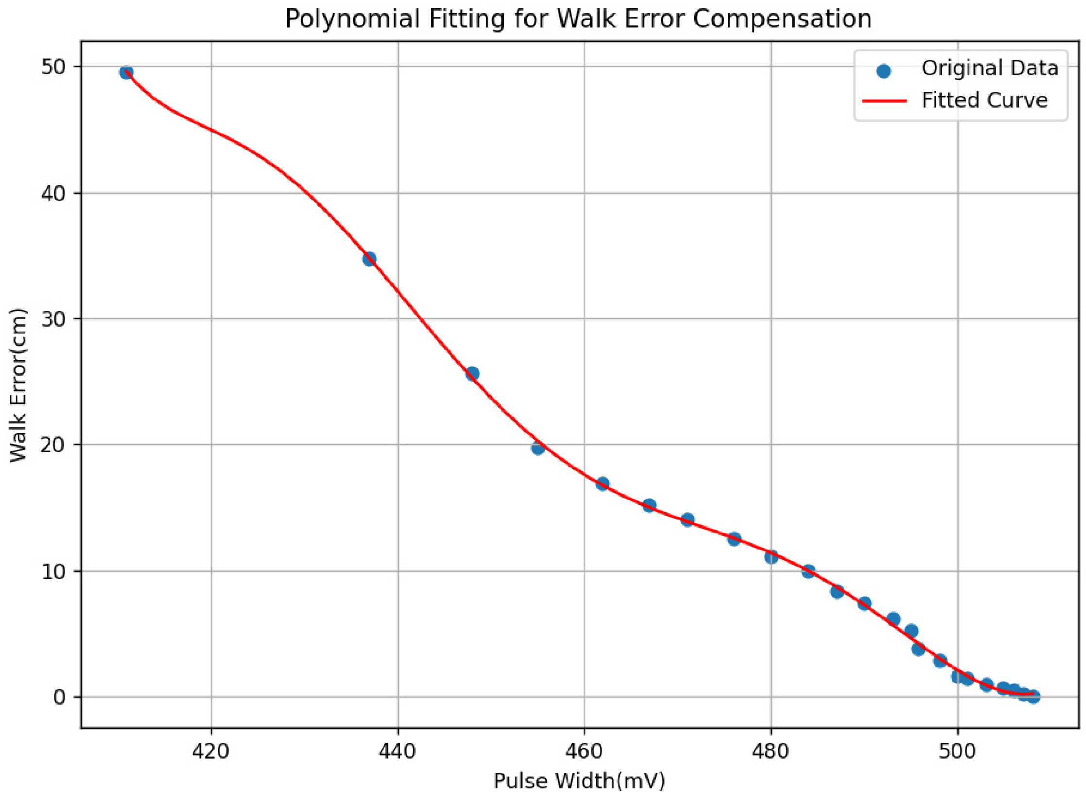
Since a high-order polynomial can potentially oscillate between data points, the fit is also evaluated using leave-one-out cross-validation. Within the densely sampled part of the window, from 448 mV to 508 mV, the RMS prediction error is 0.9 cm, close to the fitting residual, confirming that the polynomial does not overfit the data in this region. In the lower-amplitude region between 411 mV and 437 mV, where the walk error changes most rapidly and calibration samples are sparser, the fitted polynomial remains strictly monotonic without local extrema or Runge oscillations; furthermore, the compensation accuracy in this transition is directly verified by the physical ranging experiment in Figure 24, where the residual at the lowest amplitude remained below 2 cm.
Figure 24.
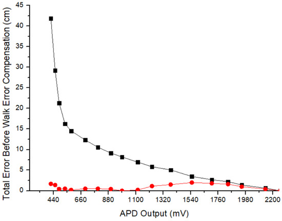
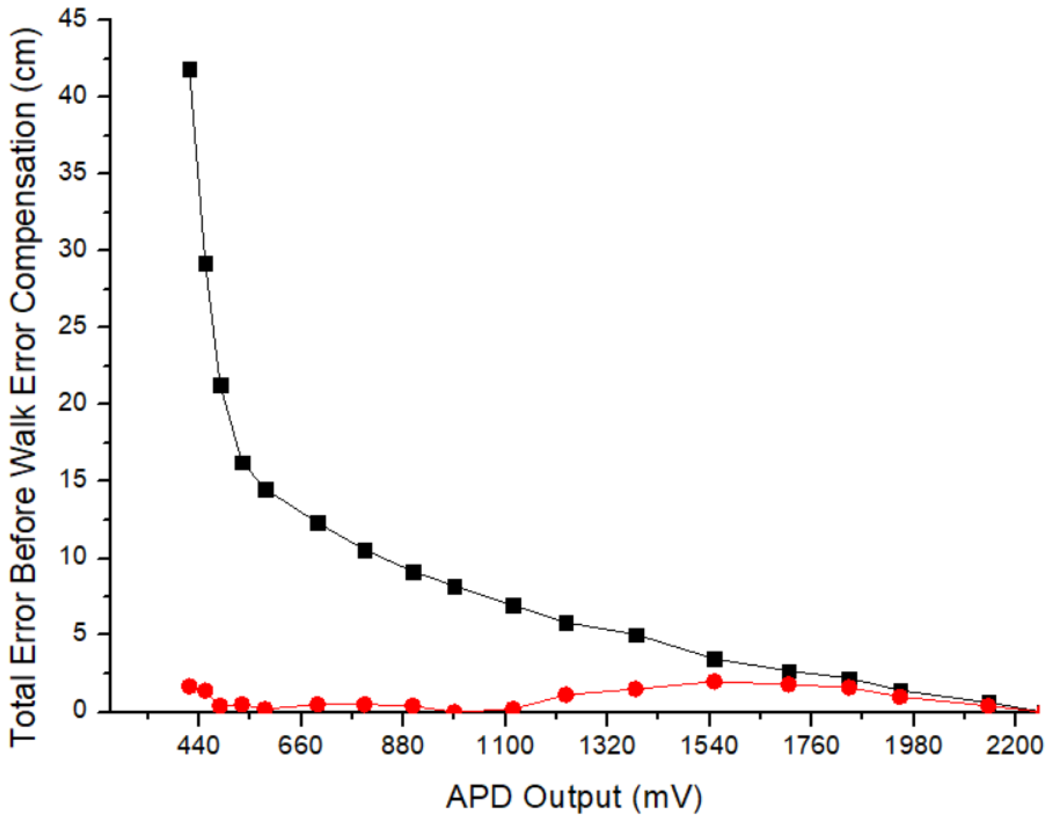
Total distance error before (black) and after (red) walk error compensation as a function of the APD output amplitude.
The polynomial is valid only within the calibrated pulse-width window, specifically for pulse-width voltages of about 411–508 mV at the TAC output, corresponding to echo pulse widths of 43–53 ns. Outside this window, a seventh-order polynomial diverges within a few millivolts in pulse width, so the correction must not be extrapolated; pulse widths outside the window should be clamped to the boundary values or flagged as out-of-range.
A follow-up experiment is performed to verify how well the fitted polynomial curve compensates for the walk error. Just as in the previous setup, the polarization filter is rotated to create a large walk error across varying optical signal levels. The overall distance error is then measured as a function of the Thorlabs APD amplitude, comparing uncompensated and compensated results. The result is shown in Figure 24. Using the proposed FPGA-based TAC alongside pulse-width measurement and polynomial fitting, the initial 42 cm total error, which occurred at the lowest APD amplitude of this verification run, is reduced to 2 cm.
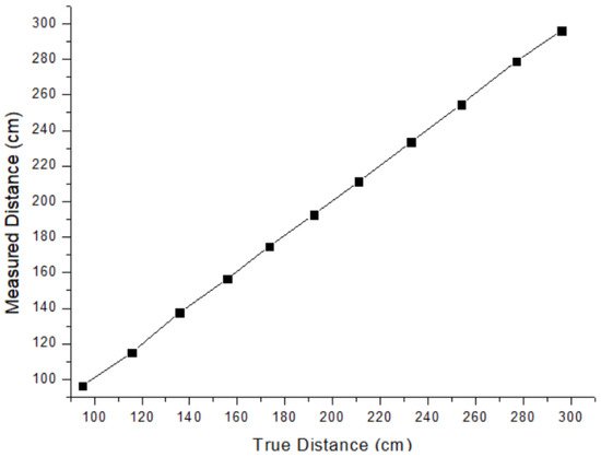
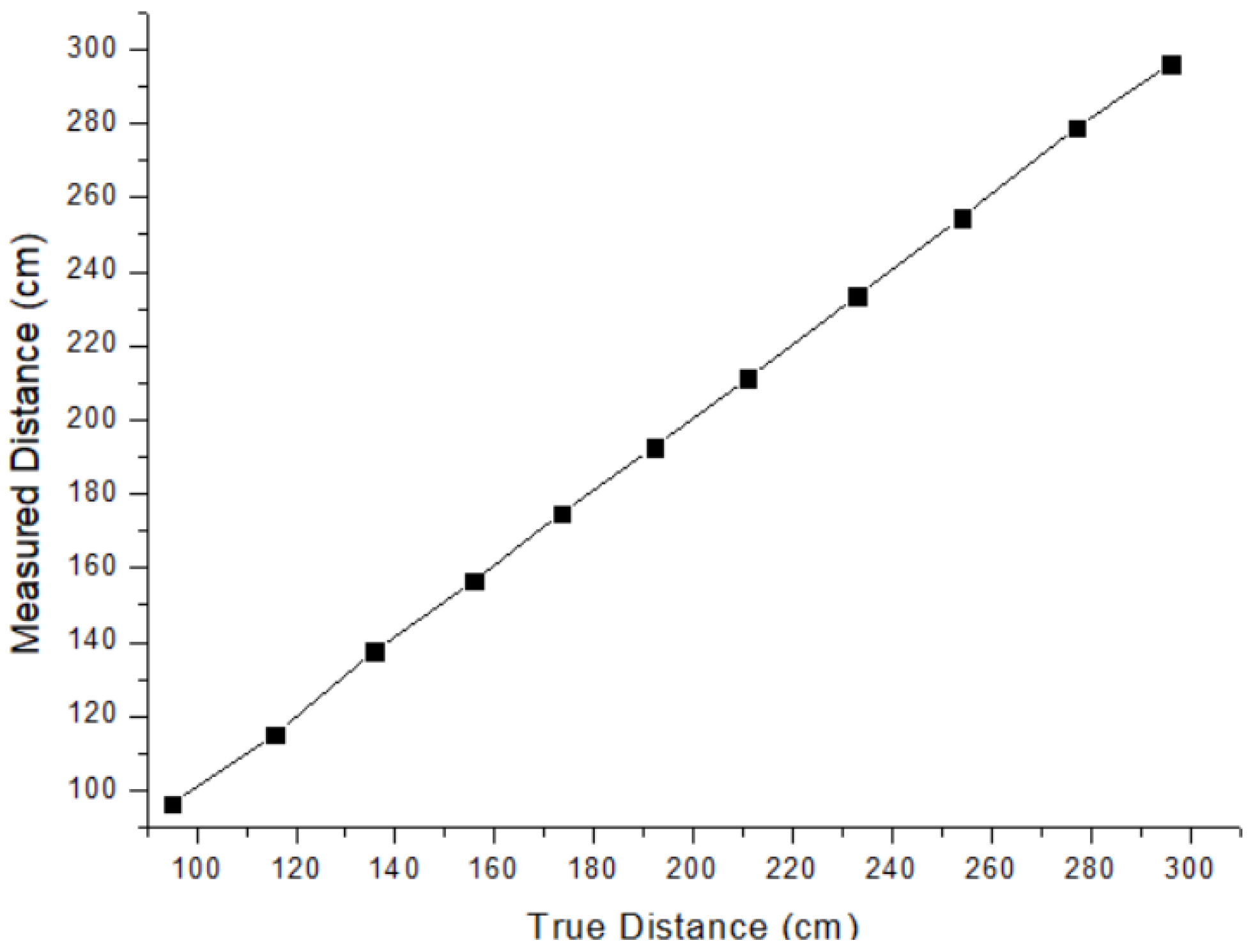
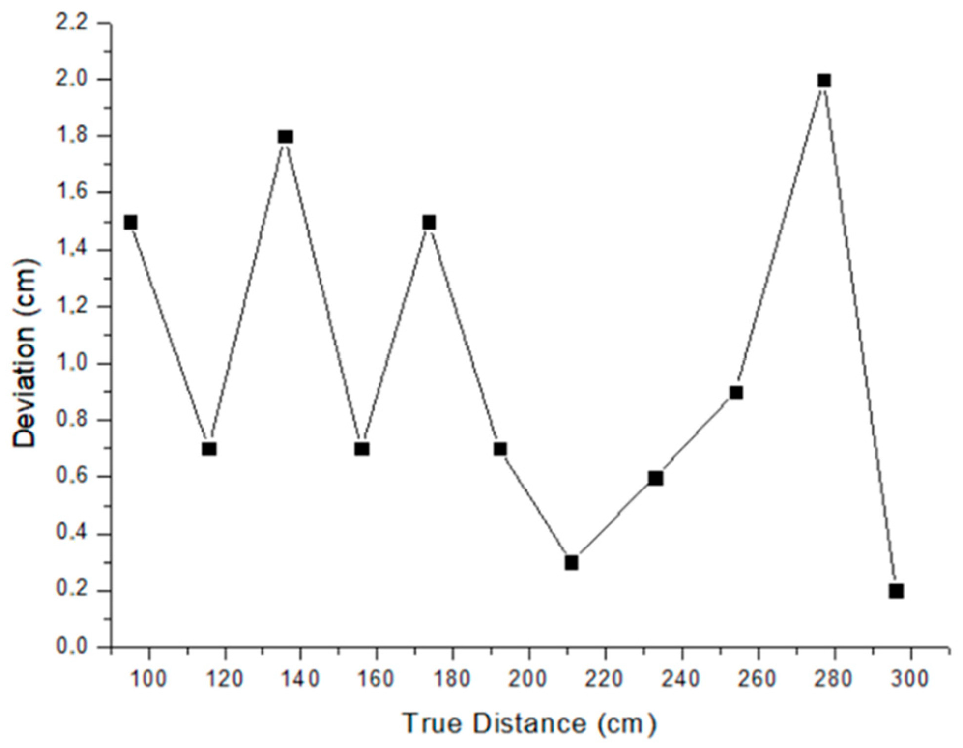
Following walk error compensation, ranging experiments are carried out to evaluate the performance of the overall LiDAR system and the proposed FPGA-based TAC. The polynomial function obtained from Figure 23 is applied for error compensation. In these experiments, the target is positioned at distances ranging from 95 cm to 296 cm in approximately 20 cm increments. Figure 25 plots the true distance measured by a commercial laser distance meter against the distance measured by our developed LiDAR system, demonstrating a highly linear relationship across the entire test range. To evaluate the system accuracy, the measurement deviation from the true distance is presented in Figure 26. The distance error ranges between 0.2 cm and 2 cm, with a maximum deviation of 2 cm observed at a target distance of 277 cm.
Figure 25.
True reference distance versus measured distance in our LiDAR experimental setup.
Figure 26.
Distance measurement deviation across the evaluated target range.
The maximum deviation of 2 cm at 277 cm can be explained by an error budget covering readout noise, front-end timing variations, and mechanical tolerances. At a TAC gain of 9.5 mV/ns, the ToF channel sensitivity is 1.58 cm/mV, meaning that an input voltage shift of only 1.3 mV produces a 2 cm ranging error. The 12-bit XADC provides a quantization step of 0.244 mV over its 1 V range, setting a baseline timing resolution of about 26 ps and a distance quantization of 3.9 mm. In contrast, because the slope of the calibration curve stays between 0.3 and 0.8 cm/mV across most of the window, millivolt-level variations in the pulse-width channel contribute only a few millimeters. Front-end timing jitter effects, including laser trigger jitter, the trigger-to-optical delay jitter of the pulsed laser, optical detector noise, and comparator overdrive dispersion, primarily influence single-shot repeatability. In addition, mechanical alignment tolerances of the target relative to the reference laser meter, combined with the 0.5 cm RMS residual of the calibration polynomial, contribute to the total uncertainty. The deviations in Figure 26 do not increase with distance and show no systematic trend, which indicates random errors rather than gain or offset errors, and the 2 cm deviation at 277 cm is consistent with this scatter.
4. Discussion
4.1. Comparison with Previous Pulse-Width-Based Compensation Methods
Table 1 compares the proposed approach with previous walk compensation methods reported in the literature. This comparison should be interpreted with fundamentally different conditions in mind, as the evaluated systems range from full-custom integrated receivers to discrete laboratory platforms like ours. These approaches fall into two main groups: one operates in the analog domain to measure the echo amplitude for signal intensity estimation, while the other conducts the estimation in the digital domain without requiring any additional analog front-end circuitry. Methods using peak detectors, AGCs, dual-threshold mechanisms, and constant-fraction discrimination compensate for the walk error in the analog domain and require additional analog circuitry in each channel. Pulse-width methods maintain a simple leading-edge receiver and shift the compensation to the time domain using pulse width information to estimate the echo intensity. The previous implementations of walk error compensation in the literature are based on ASIC-based TDCs [26,28,29], commercial TDC ICs [31,32], or FPGA TDCs [6].
Table 1.
Comparison of walk error compensation methods.
Dedicated ASIC receiver–TDC approaches show better performance compared with the present system in terms of residual walk error, dynamic range, and single-shot capability, and the proposed method does not intend to compete with them. Instead, its primary contribution lies in shifting the measurement complexity by transforming a sub-nanosecond timing problem into a straightforward DC voltage amplitude measurement. One can measure the phase shift with picosecond-order resolution without designing a complex ASIC chip and waiting for long production and test times, but rather by using a low-complexity and low-cost circuit consisting of only a DFF and a buffered RC filter.
Both ToF and echo pulse width are converted directly into DC voltage levels, completely eliminating the need for high-speed reference clocks and tapped delay lines. This removes the need for detailed bin-by-bin calibration typically required to compensate for PVT variations and non-uniform propagation delays across individual elements. Compared with our previous DPS-based TDC [6], which achieved a similar 0-to-3 cm residual error under identical optical conditions, this TAC architecture requires neither iterative phase sweeps of the laser trigger nor dedicated digital counters in each channel. The hardware footprint is minimal. A ToF channel consumes just one D flip-flop, while the pulse-width channel requires zero FPGA logic, relying entirely on a low-cost external RC filter and buffer. Consequently, system scalability is limited only by available I/O pins and ADC inputs rather than digital logic resources. Because the measurement outputs are slowly varying DC levels, a single multichannel ADC can seamlessly digitize many channels in sequence. While this work establishes the fundamental method using a single channel, the fully multiplexed implementation for our 3D LiDAR is the primary focus of our ongoing work.
4.2. Clock-Free Conversion: Advantages and Limits
High-performance TDCs, whether implemented in an ASIC or an FPGA, mostly obtain their high resolution from the utilization of both a high-speed clock and a delay line based on Nutt interpolation. The start and stop events are asynchronous to the reference clock, and an event close to a clock edge can result in metastability in the rest of the digital logic due to setup/hold violations. This metastability and routing-skew-induced delay between the coarse counter and the delay line for the fine time measurement can result in an off-by-one counting ambiguity, causing a one-period timing error [33]. Dual-edge synchronizers have been proposed as a remedy [34]. However, the asynchronous nature of the start and stop events is inevitable. At 200 MHz, a single-cycle counting error results in a 5 ns ToF error, corresponding to a 75 cm distance error.
In the proposed TAC, no event is sampled by a high-speed clock. The transmitted pulse and the echo pulse are connected directly to the clock asynchronous-clear inputs of the DFF, resulting in a digital signal having the same period as the transmitted signal and a width proportional to the ToF of the light. The output is connected directly to an RC filter that averages the resulting duty cycle, providing a DC output signal whose amplitude is proportional to the ToF information. Therefore, a coarse-count error cannot occur.
Fundamentally, the resolution of a high-performance TDL-based FPGA TDC is the propagation delay of a carry cell. We showed in [12] that the propagation delay of carry cells changes between 17.85 ps and 21.7 ps over a temperature range of −30 °C to 105 °C, resulting in a change of more than 1 ns over a delay line with a 5 ns total propagation delay. The same measurement chain was applied to the TAC presented in [12]. The temperature was varied in an environmental chamber between 3 °C and 93 °C, and the supply voltages were swept from ±3.5 V to ±10 V to test the TAC against PVT variations. The phase-shift measurement of the TAC changed by only 3.3 mV (about 32 ps) over the full temperature range, and the supply sweep changed the output by at most 2.2 mV. We can assume that replacing the XOR gate with a DFF leaves the structure of the TAC chain functionally untouched, since there is no delay line with a large propagation delay, and the circuitry outside the FPGA remains identical, utilizing the same I/O drivers, passive filters, and buffers. Therefore, these results underline the PVT resilience of our FPGA-based TAC presented in this article. The temperature dependence of the optical front-end (APD gain, laser pulse shape, and comparator threshold) can affect the walk error calibration; however, since it is constructed from discrete components, we cannot place the entire setup inside a temperature chamber. Rather, we focus on the walk error compensation capability of the proposed TAC.
The absence of bins also removes most of the calibration effort and makes the design portable. A TDL-based TDC needs a bin-by-bin characterization, usually a code density test with a large number of random hits or a DPS sweep [12], which is specific to the device, to the placement of the line and to the operating temperature; moving the design to another FPGA, or to another die of the same family, changes the bin widths and requires a new calibration [35,36]. Our FPGA-based TAC relies on a single DFF primitive instead of carry chains, so it has no internal routing bottlenecks, needs no manual floor planning (Pblocks) and is largely insensitive to placement on the die. The design fits any FPGA or CPLD that provides a DFF with an asynchronous clear, regardless of the carry-chain structure, and its analog part consists of passive components and two operational amplifiers, whereas ASIC TDCs, which achieve the best absolute performance, are tied to a semiconductor process and to the long design and fabrication cycles of custom silicon. No high-speed clock is needed in the measurement path either: the FPGA clock serves only the XADC readout and communication, so clock jitter, clock distribution skew and the phase alignment of multiphase clocks do not degrade the measurement.
The inherent trade-off of the averaging conversion is that the FPGA-based TAC is not a single-shot converter: its output settles with a time constant and represents the mean over multiple laser periods. The method is, therefore, best suited to high-repetition-rate ranging applications that do not require single-shot measurements. Because compensation depends on this time-averaged mean, multiple echoes within a single period—for example, from partially transparent targets or rain—cannot be resolved individually.
4.3. Measurement Range, Atmospheric Attenuation and Weak Echoes
Our ranging experiments are limited to about 3 m by practical laboratory constraints: the prototype is an indoor benchtop setup built from discrete optoelectronic components, and its laser (Thorlabs NPL79B, 785 nm, 88 mW peak optical power) is far weaker than the 75 W source modeled in Section 2 for long-range scenarios. Since walk error results from echo amplitude fluctuations, a polarizing filter is used to vary the signal amplitude at a fixed distance. This allows the walk error compensation to be evaluated over a wide range of signal levels, while the optical alignment remains unchanged within the 3 m measurement range.
The measurable time interval of the FPGA-based TAC is set by the laser repetition period T and by the input voltage range of the ADC. The conversion gain is k = VOH/T with VOH ≈ 3.4 V, the logic-high level of the FPGA output, i.e., 9.5 mV/ns for T = 360 ns, and the unambiguous range cT/2 (where c is the speed of light) is 54 m for a 2 MHz repetition rate. In the present configuration, the 1 V input range of the XADC limits the usable duty cycle to about 29%, i.e., to intervals of about 105 ns including fixed system delays.
According to Equation (1), which defines the received peak power, atmospheric attenuation introduces an exponential decay factor. In clear air or light haze, this attenuation simply scales down the echo amplitude without distorting the pulse shape. Because our calibration curve specifically tracks these amplitude variations, the walk error compensation remains fully valid as long as the weakened echo stays within the calibrated detection window. Consequently, the main impact of atmospheric attenuation is a reduction in the maximum measurement range, rather than a failure of the compensation method itself. To illustrate these operational boundaries, we apply the extinction model of Kim et al. [39] at the standard 905 nm automotive wavelength, although our laboratory prototype operates at 785 nm. Based on this model, the threshold-limited range for a 50% target reflectivity with a 600 mV threshold drops from 405 m in clear air to 375 m at 10 km visibility, 212 m at 1 km visibility, and 82 m in fog with 200 m visibility. In contrast, operating with a 100 mV threshold extends these respective ranges to 991 m, 836 m, 346 m, and 112 m.
However, severe weather conditions such as dense fog, rain, and snow introduce multiple scattering, which distorts the temporal profile of the echo [40]. While free-space optical links typically mitigate this scintillation through dynamic adaptive thresholding [41], our proposed pulse-width method natively treats this modulation as just another amplitude variation that the calibration curve tracks within the validated window. In contrast, a temporally distorted echo fundamentally breaks the monotonic relationship between pulse width and walk error, similar to the effect of overlapping multi-target echoes. If multiple scattering broadens the pulse, the pulse width alone ceases to be a reliable compensation variable. Under these conditions, the system requires additional shape information, such as the slew rate [28,30], or a rigorous plausibility check on the measured width.
Weak echoes represent the most challenging regime for the method. As the echo amplitude approaches the threshold, the digital echo narrows and the walk error grows most rapidly, mainly due to the overdrive dispersion of the comparator. So, the calibration curve is steepest where the signal-to-noise ratio is lowest. The averaging of the TAC reduces the random part of this jitter, roughly by the square root of the number of averaged pulses, but not the bias of missed detections described in Section 4.2. A higher threshold gives a cleaner pulse-width measurement at the price of sensitivity, 7.8 dB or a factor of 2.45 in clear-air range for the step from 100 mV to 600 mV, as quantified in the Walk Error Simulations section. The calibration curve needs to be maintained for each threshold setting. With such a set of curves, the method is also compatible with adaptive thresholds that follow the operating conditions, for example, the constant-false-alarm-rate (CFAR) threshold control used to suppress background noise in LiDAR receivers [42]. At the system level, high-fidelity sensor validation [43] and adaptive perception algorithms [44] then determine how reliably the corrected ranges can be used in automated driving and robotics.
5. Conclusions
To the best of our knowledge, this is the first time an FPGA-based TAC has been utilized as a ToF sensor in a LiDAR system that inherently provides walk error compensation through simultaneous pulse-width measurement. Existing implementations of pulse width-based walk error compensation are based on TDCs. They have excellent resolution and precision in ToF and pulse width measurement. However, because their resolution relies on high-speed clocks for coarse time and delay lines for fine-time measurements, they inherently suffer from coarse-count ambiguity, bin calibration requirements, high logic resource consumption, sensitivity to PVT variations, and portability limitations.
We demonstrated in [12] that a low-cost and low-complexity FPGA-based TAC can be used to measure the phase shift as low as 18 ps. It was promising for scalability for multichannel operation due to its low resource consumption, requiring only one XOR gate inside the FPGA fabric and a simple buffered RC low-pass filter outside of the FPGA. In addition, it was very resilient to PVT variations; a 90 °C variation deviates the phase measurement by only 32 ps. However, we realized in our later experiments that the FPGA-based TAC is insufficient to be used in LiDAR systems due to its vulnerability to echo signal intensity fluctuations.
This article presents an enhancement of our previous TAC architecture through an improved phase detection method and the addition of a second channel for simultaneous pulse-width measurement. The resulting hardware footprint is notably minimal. Specifically, the ToF channel utilizes only a single DFF, and the pulse-width channel requires no FPGA logic. The channels require only a low-cost and low-complexity externally buffered RC filter outside of the FPGA. As a result, the scalability of the system is constrained only by the available I/O pins and ADC inputs instead of digital logic resources.
The proposed FPGA-based TAC operates using a single DFF primitive rather than delay lines with conventional carry chains. This approach prevents internal routing bottlenecks, avoids the need for manual floor planning such as Pblocks, and makes the system highly insensitive to physical placement on the die. Consequently, the architecture can be implemented on any FPGA or CPLD. Although ASIC TDCs provide the highest absolute performance, they remain restricted by specific semiconductor processes and lengthy custom silicon fabrication cycles. Additionally, the measurement path completely omits high-speed clocks. Therefore, the system remains immune to measurement degradation caused by clock jitter, clock distribution skew, and multiphase clock alignment issues.
We conducted experiments to test the proposed method and the FPGA-based TAC in our experimental LiDAR system. We observed that the walk-induced ranging error is significantly reduced from 42 cm to 2 cm. Furthermore, the system measures target distances within a maximum error of 2 cm for target ranges from 0.95 m to 2.96 m. These results reveal that our novel FPGA-based TAC measures the ToF of light with high precision and shows strong resilience to the large echo signal intensity variations that a LiDAR system encounters during real-life operation due to different target ranges and reflectivities. Therefore, we believe that this high-precision ToF measurement and walk error compensation capability, alongside its very low cost, low complexity, and high scalability, will provide a promising solution for LiDAR sensors. Our future work aims to extend the FPGA-based TAC architecture into a dense multichannel receiver to be used in high-performance 3D LiDAR systems.
Author Contributions
Conceptualization, A.O.K., H.Y; methodology, A.O.K., H.Y.; software, A.O.K.; validation, A.O.K. and H.Y.; formal analysis, A.O.K.; investigation, A.O.K.; resources, A.O.K. and H.Y.; data curation, A.O.K.; writing—original draft preparation, A.O.K.; writing—review and editing, A.O.K. and H.Y.; visualization, A.O.K. All authors have read and agreed to the published version of the manuscript.
Funding
This research received no external funding.
Data Availability Statement
The data presented in this study are available within the article.
Conflicts of Interest
The authors declare no conflict of interest.
References
- Kalisz, J. Review of methods for time interval measurements with picosecond resolution. Metrologia 2004, 41, 17–32. [Google Scholar] [CrossRef] [Scilit]
- Nutt, R. Digital time intervalometer. Rev. Sci. Instrum. 1968, 39, 1342–1345. [Google Scholar] [CrossRef] [Scilit]
- Wang, Y.; Liu, C. A 3.9 ps time-interval RMS precision time-to-digital converter using a dual-sampling method in an UltraScale FPGA. IEEE Trans. Nucl. Sci. 2016, 63, 2617–2621. [Google Scholar] [CrossRef] [Scilit]
- Szplet, R.; Czuba, A. Two-stage clock-free time-to-digital converter based on Vernier and tapped delay lines in FPGA device. Electronics 2021, 10, 2190. [Google Scholar] [CrossRef] [Scilit]
- Balla, A.; Beretta, M.M.; Ciambrone, P.; Gatta, M.; Gonnella, F.; Iafolla, L.; Mascolo, M.; Messi, R.; Moricciani, D.; Riondino, D. The characterization and application of a low resource FPGA-based time to digital converter. Nucl. Instrum. Methods Phys. Res. A 2014, 739, 75–82. [Google Scholar] [CrossRef] [Scilit]
- Korkan, A.O.; Yuksel, H. A 32-Channel, Low Resources and High-Precision FPGA Time-to-Digital Converter (TDC) Based on Dynamic Phase Shifting (DPS) for 3-D LiDAR Applications. IEEE Trans. Instrum. Meas. 2026, 75, 9506914. [Google Scholar] [CrossRef] [Scilit]
- Crotti, M.; Rech, I.; Ghioni, M. Four channel, 40 ps resolution, fully integrated time-to-amplitude converter for time-resolved photon counting. IEEE J. Solid-State Circuits 2012, 47, 699–708. [Google Scholar] [CrossRef] [Scilit]
- Acconcia, G.; Crotti, M.; Antonioli, S.; Rech, I.; Ghioni, M. High performance time-to-amplitude converter array. In Proceedings of the 2013 IEEE Nordic-Mediterranean Workshop on Time-to-Digital Converters (NoMe TDC), Perugia, Italy, 3 October 2013; pp. 1–5. [Google Scholar]
- Wu, Z.; Xu, Y.; Ma, Z. A time-to-amplitude converter with high impedance switch topology for single-photon time-of-flight measurement. IEEE Access 2021, 9, 16672–16678. [Google Scholar] [CrossRef] [Scilit]
- Kanoun, M.; Bérubé-Lauzière, Y.; Fontaine, R. High precision time-to-amplitude converter for diffuse optical tomography applications. In Proceedings of the 3rd International Conference on Design and Technology of Integrated Systems in Nanoscale Era (DTIS), Tozeur, Tunisia, 25–27 March 2008; pp. 1–4. [Google Scholar]
- Choi, S.; Chon, Y.; Park, S.M. A Low-Power Optoelectronic Receiver IC for Short-Range LiDAR Sensors in 180 nm CMOS. Micromachines 2024, 15, 1066. [Google Scholar] [CrossRef] [Scilit] [PubMed]
- Korkan, A.O.; Yuksel, H. A Novel Time-to-Amplitude Converter and a Low-Cost Wide Dynamic Range FPGA TDC for LiDAR Application. IEEE Trans. Instrum. Meas. 2022, 71, 2005015. [Google Scholar] [CrossRef] [Scilit]
- Yang, R.; Tang, Y.; Fu, Z.; Qiu, J.; Liu, K. A Method of Range Walk Error Correction in SiPM LiDAR with Photon Threshold Detection. Photonics 2022, 9, 24. [Google Scholar] [CrossRef] [Scilit]
- Wang, Z.; Wang, Y.; Ma, Q.; Wu, Y. Optimization of a Range Walk Error Correction for Underwater Photon Counting LiDAR Under Low-Photon Conditions. Photonics 2026, 13, 427. [Google Scholar] [CrossRef] [Scilit]
- Wang, X.; Ma, R.; Li, D.; Zheng, H.; Liu, M.; Zhu, Z. A Low Walk Error Analog Front-End Circuit with Intensity Compensation for Direct ToF LiDAR. IEEE Trans. Circuits Syst. I Regul. Pap. 2020, 67, 4309–4321. [Google Scholar] [CrossRef] [Scilit]
- Palojärvi, P.; Ruotsalainen, T.; Kostamovaara, J. A 250-MHz BiCMOS receiver channel with leading edge timing discriminator for a pulsed time-of-flight laser rangefinder. IEEE J. Solid-State Circuits 2005, 40, 1341–1349. [Google Scholar] [CrossRef] [Scilit]
- Zheng, H.; Ma, R.; Wang, X.; Liu, M.; Zhu, Z. A CMOS Peak Detect and Hold Circuit With Auto-Adjust Charging Current for NS-Scale Pulse ToF Lidar Application. IEEE Trans. Circuits Syst. I Regul. Pap. 2020, 67, 4409–4419. [Google Scholar] [CrossRef] [Scilit]
- Sędek, B.; Zygmunt, M.; Jakubaszek, M.; Drozd, T.; Wojtanowski, J. Real-Time Walk Error Compensation Method Using Echo Signal Magnitude Measurement in ToF Laser Scanners. Sensors 2024, 24, 733. [Google Scholar] [CrossRef] [Scilit] [PubMed]
- Choi, Y.-H.; Kuc, T.-Y. Walk Error Compensation of ToF LiDAR using Zero Crossing Discriminator with Auto Gain Control Amplifier. In Proceedings of the 22nd International Conference on Control, Automation and Systems (ICCAS), Jeju, Republic of Korea, 27–30 November 2022; pp. 1461–1468. [Google Scholar]
- Lim, H. Constant Fraction Discriminator Involving Automatic Gain Control to Reduce Time Walk. IEEE Trans. Nucl. Sci. 2014, 61, 2351–2356. [Google Scholar] [CrossRef] [Scilit]
- Li, X.; Wang, H.; Yang, B.; Huyan, J.; Xu, L. Influence of Time-Pickoff Circuit Parameters on LiDAR Range Precision. Sensors 2017, 17, 2369. [Google Scholar] [CrossRef] [Scilit] [PubMed]
- Yang, J.; Liu, X.; Gu, G.; Qian, W.; Ren, K.; Zhang, J.; Guo, P.; Gao, Q.; Chen, Q. A double threshold correction method for walk error in pulsed laser ranging system. Infrared Phys. Technol. 2019, 100, 28–36. [Google Scholar] [CrossRef] [Scilit]
- Cho, H.-S.; Kim, C.-H.; Lee, S.-G. A High-Sensitivity and Low-Walk Error LADAR Receiver for Military Application. IEEE Trans. Circuits Syst. I Regul. Pap. 2014, 61, 3007–3015. [Google Scholar] [CrossRef] [Scilit]
- Nissinen, J.; Nissinen, I.; Kostamovaara, J. Integrated Receiver Including Both Receiver Channel and TDC for a Pulsed Time-of-Flight Laser Rangefinder With cm-Level Accuracy. IEEE J. Solid-State Circuits 2009, 44, 1486–1497. [Google Scholar] [CrossRef] [Scilit]
- Kurtti, S.; Kostamovaara, J. Pulse width time walk compensation method for a pulsed time-of-flight laser rangefinder. In Proceedings of the 2009 IEEE Instrumentation and Measurement Technology Conference (I2MTC), Singapore, 5–8 May 2009; pp. 1059–1062. [Google Scholar]
- Kurtti, S.; Kostamovaara, J. An Integrated Laser Radar Receiver Channel Utilizing a Time-Domain Walk Error Compensation Scheme. IEEE Trans. Instrum. Meas. 2011, 60, 146–157. [Google Scholar] [CrossRef] [Scilit]
- Jansson, J.-P.; Mäntyniemi, A.; Kostamovaara, J. A CMOS time-to-digital converter with better than 10 ps single-shot precision. IEEE J. Solid-State Circuits 2006, 41, 1286–1296. [Google Scholar] [CrossRef] [Scilit]
- Kurtti, S.; Nissinen, J.; Kostamovaara, J. A Wide Dynamic Range CMOS Laser Radar Receiver With a Time-Domain Walk Error Compensation Scheme. IEEE Trans. Circuits Syst. I Regul. Pap. 2017, 64, 550–561. [Google Scholar] [CrossRef] [Scilit]
- Kurtti, S.; Jansson, J.-P.; Kostamovaara, J. A CMOS Receiver–TDC Chip Set for Accurate Pulsed TOF Laser Ranging. IEEE Trans. Instrum. Meas. 2020, 69, 2208–2217. [Google Scholar] [CrossRef] [Scilit]
- Choe, K.H.; Choe, U.C.; Ri, I.J. Correction method for walk error based on the shape of reflective surface in LiDAR. Optik 2023, 279, 170527. [Google Scholar] [CrossRef] [Scilit]
- Yan, S.; Yang, G.; Li, Q.; Wang, Y.; Wang, C. Research of Distance-Intensity Imaging Algorithm for Pulsed LiDAR Based on Pulse Width Correction. Remote Sens. 2022, 14, 507. [Google Scholar] [CrossRef] [Scilit]
- Pogačnik, L.; Munih, M. Modular Lidar System for Multiple Field-of-View Ranging. Sensors 2024, 24, 84. [Google Scholar] [CrossRef] [Scilit] [PubMed]
- Jansson, J.-P.; Mäntyniemi, A.; Kostamovaara, J. Synchronization in a Multilevel CMOS Time-to-Digital Converter. IEEE Trans. Circuits Syst. I Regul. Pap. 2009, 56, 1622–1634. [Google Scholar] [CrossRef] [Scilit]
- Szplet, R.; Kalisz, J.; Jachna, Z. A 45 ps time digitizer with a two-phase clock and dual-edge two-stage interpolation in a field programmable gate array device. Meas. Sci. Technol. 2009, 20, 025108. [Google Scholar] [CrossRef] [Scilit]
- Won, J.Y.; Lee, J.S. Time-to-digital converter using a tuned-delay line evaluated in 28-, 40-, and 45-nm FPGAs. IEEE Trans. Instrum. Meas. 2016, 65, 1678–1689. [Google Scholar] [CrossRef] [Scilit]
- Machado, R.; Cabral, J.; Alves, F.S. Recent developments and challenges in FPGA-based time-to-digital converters. IEEE Trans. Instrum. Meas. 2019, 68, 4205–4221. [Google Scholar] [CrossRef] [Scilit]
- Analog Devices. LTC6268-10 Datasheet: 4 GHz Ultra-Low Bias Current FET Input Op Amp. 2017. Available online: https://www.analog.com/media/en/technical-documentation/data-sheets/626810f.pdf (accessed on 17 July 2026).
- Analog Devices. LTC6752 Comparator Family Datasheet: 280 MHz, 2.9 ns Comparator with Rail-to-Rail Inputs and CMOS Outputs. 2017. Available online: https://www.analog.com/media/en/technical-documentation/data-sheets/6752fc.pdf (accessed on 17 July 2026).
- Kim, I.I.; McArthur, B.; Korevaar, E.J. Comparison of laser beam propagation at 785 nm and 1550 nm in fog and haze for optical wireless communications. Proc. SPIE 2001, 4214, 26–37. [Google Scholar] [CrossRef] [Scilit]
- Rasshofer, R.H.; Spies, M.; Spies, H. Influences of weather phenomena on automotive laser radar systems. Adv. Radio Sci. 2011, 9, 49–60. [Google Scholar] [CrossRef] [Scilit]
- Tian, D.; Zhang, P.; Yu, H.; Wang, Y.; Zhang, Y.; Zhang, P.; Tong, S. Dynamic Adaptive Threshold Decision for Real-Time Optical Communication Systems in Turbulence Channels. J. Light. Technol. 2026, 44, 2919–2924. [Google Scholar] [CrossRef] [Scilit]
- Jiang, Y.; Zhu, J.; Jiang, C.; Xie, T.; Liu, R.; Wang, Y. Adaptive Suppression Method of LiDAR Background Noise Based on Threshold Detection. Appl. Sci. 2023, 13, 3772. [Google Scholar] [CrossRef] [Scilit]
- Zhu, B.; Cao, X.; Zhang, P.; Zhao, J.; Han, J.; Tang, R. High-Fidelity Ultrasonic Radar In-the-Loop Accelerated Test for Automatic Parking Systems. IEEE Trans. Intell. Transp. Syst. 2025, 26, 17055–17067. [Google Scholar] [CrossRef] [Scilit]
- Zhang, R.; Wang, Y.; Li, Z.; Ding, F.; Wei, C.; Wu, M. Online Adaptive Keypoint Extraction for Visual Odometry Across Different Scenes. IEEE Robot. Autom. Lett. 2025, 10, 7539–7546. [Google Scholar] [CrossRef] [Scilit]

Disclaimer/Publisher’s Note: The statements, opinions and data contained in all publications are solely those of the individual author(s) and contributor(s) and not of MDPI and/or the editor(s). MDPI and/or the editor(s) disclaim responsibility for any injury to people or property resulting from any ideas, methods, instructions or products referred to in the content. |
© 2026 by the authors. Licensee MDPI, Basel, Switzerland. This article is an open access article distributed under the terms and conditions of the Creative Commons Attribution (CC BY) license.