


Abstract
Silicon carbide (SiC) has emerged as a critical wide-bandgap semiconductor for power electronics. However, its high optical transmittance and relatively low dielectric contrast impose fundamental limitations on nanoscale defect detection compared with conventional silicon (Si) wafers. In this work, a numerical framework combining the finite-difference time-domain (FDTD) method with vectorial Debye–Wolf theory is developed. Comparison of the optical responses of Si and 4H-SiC identifies a dual degradation mechanism in 4H-SiC darkfield inspection: roughness-induced background enhancement associated with high transmittance and defect signal attenuation caused by the lower dielectric contrast. To improve the signal-to-noise ratio (SNR) and defect intensity, the effects of incidence angle and polarization state on defect scattering are investigated, and the illumination configuration is optimized accordingly. A 405 nm polarization-tunable laser scattering darkfield imaging system is developed for 4H-SiC wafer inspection, enabling high-SNR detection of 100 nm-diameter polystyrene latex (PSL) particles and effective identification of practical morphological defects. The experimental results agree with the numerical predictions, validating the effectiveness of system optimization guided by defect scattering characteristics. This work elucidates the material-dependent mechanisms limiting darkfield inspection sensitivity in SiC wafers and provides a viable pathway toward high-sensitivity detection of nanoscale morphological defects.
1. Introduction
As a representative third-generation wide-bandgap semiconductor, SiC is driving a revolution in energy efficiency in applications such as electric vehicles and smart grids, enabled by its exceptional high-voltage and high-current handling capabilities [1,2,3]. However, defects are inevitably introduced during SiC single-crystal growth and epitaxial processing, which critically degrade device yield and long-term reliability [4,5]. According to their spatial characteristics, SiC defects are generally categorized into crystallographic defects and morphological defects. Surface/near-surface morphological defects, such as particle contamination, triangular defects, and scratches, are particularly prevalent and have been demonstrated to adversely affect the breakdown voltage, leakage current, and operational lifetime of devices [6,7]. Therefore, the development of high-sensitivity, non-contact, and inline-compatible defect inspection technologies is crucial for achieving high-yield SiC device manufacturing.
Morphological defects on SiC wafers can be characterized using optical microscopy (OM), differential interference contrast (DIC) microscopy, atomic force microscopy (AFM), and scanning electron microscopy (SEM) [4]. Among these techniques, optical inspection is widely used for wafer-quality screening because of its high throughput and compatibility with industrial process monitoring [8,9]. Considerable efforts have therefore been devoted to SiC wafer defect inspection. For example, Harada et al. developed the XS-1 Sirius system for detecting macroscopic surface defects on SiC substrates [10,11]. Wang et al. introduced a tunable virtual pinhole into an oblique-incidence line-confocal imaging system to enhance defect contrast [12]. In addition, photoluminescence (PL) imaging [13], optical coherence tomography (OCT) [9], and X-ray diffraction (XRD) [14] have been applied to the characterization of different types of SiC defects. More broadly, recent advances in optical surface metrology have demonstrated considerable potential for three-dimensional surface characterization and quantitative profiling [15,16,17]. Although these methods are well suited to quantitative surface-profile reconstruction, the high-sensitivity detection of weakly scattering and low-contrast defects remains challenging. For SiC wafers in particular, existing studies have primarily focused on micrometer-scale defects [9,18,19,20], whereas defects with weak scattering signatures have received comparatively limited attention. Moreover, well-established optical scattering inspection techniques have been widely developed for Si semiconductor manufacturing [21,22,23], but their direct application to SiC is hindered by the substantial differences in optical properties between the two materials. The effects of material-dependent optical properties on defect scattering have not yet been fully elucidated in SiC wafer inspection, thereby limiting further improvements in detection sensitivity.
Numerical simulations are first performed to compare the scattering behavior of Si and 4H-SiC substrates. The results indicate a dual sensitivity degradation mechanism in darkfield inspection of 4H-SiC wafers, consisting of roughness-induced background enhancement and defect signal attenuation. Subsequently, leveraging the FDTD method and vectorial Debye–Wolf theory, the illumination-dependent optical responses of representative nanoscale morphological defects are investigated. Based on these insights, a polarization-tunable oblique-incidence darkfield inspection system is developed. Experiments with 100 nm-diameter PSL particles deposited on the wafer surface confirm the system’s sensitivity to nanoscale defects, while successful imaging of practical wafer defects demonstrates its applicability to morphological-defect inspection. The proposed method provides a basis for the further development of highly sensitive in-line inspection technologies for wide-bandgap semiconductor wafers.
2. Theoretical Framework and Numerical Methods
2.1. FDTD Simulation Model
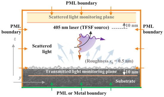
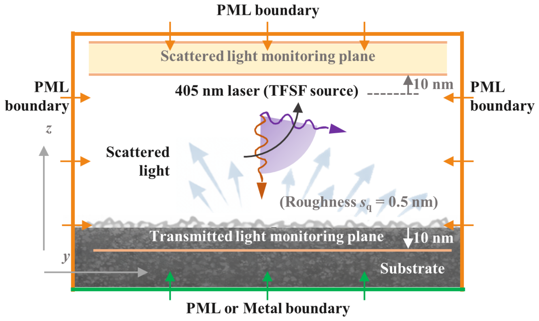
To enable high-fidelity analysis of scattering from nanoscale morphological defects, a simulation framework is established using the FDTD method [24]. As shown in Figure 1, the model incorporates both the optical configuration of the inspection system and the physical properties of the wafer.
Figure 1.
Schematic diagram of the FDTD-based simulation model.
2.1.1. Simulation Environment Configuration
Perfectly matched layer (PML) boundary conditions are applied along the x- and y-directions to suppress spurious reflections from computational boundaries. In practical wafer inspection systems, the wafer is typically supported by a sample stage. Transmitted light may be reflected or scattered by the stage back into the upper half-space, thereby elevating the stray-light background. This effect is particularly pronounced for highly transparent materials such as 4H-SiC. Consequently, the boundary condition along the z-direction is tailored to emulate this physical scenario.
Given that a wavelength of 405 nm in the visible spectrum enhances the scattering response of nanoscale defects while avoiding the potential photodamage associated with shorter ultraviolet wavelengths, this study focuses on an inspection method operating at 405 nm. A total-field scattered-field (TFSF) source with a wavelength of 405 nm serves as the incident excitation. Monitors are placed 10 nm above the TFSF source and 10 nm below the substrate to record the scattered and transmitted optical fields, respectively.
2.1.2. Wafer Substrate and Surface Defect Modeling
To approximate a realistic wafer topography, a roughness profile is introduced at the substrate interface. The root-mean-square (RMS) roughness Sq is set to 0.5 nm, with a correlation length of 100 nm.
Particle and triangular defects are prevalent morphological defects on 4H-SiC epitaxial layers. Particle defects primarily originate from particulate inclusions introduced during epitaxial growth and can act as nucleation sites for crystallographic defects within the epitaxial layer, thereby adversely affecting device yield [25]. Triangular defects arise from the disruption of atomic step flow during epitaxial growth, often induced by foreign particles, threading screw dislocations (TSDs), or surface scratches [4]. These defective regions are typically accompanied by pronounced stress fields, which can significantly degrade the electrical performance of p-n diodes [26]. Given that particle and triangular defects differ substantially in morphology, dimensions, and spatial distribution, they are selected as representative defect models in this study.
Particle defects are modeled as PSL spheres located on the surface of a 4H-SiC substrate, with a diameter D = 100 nm and a refractive index n = 1.599 [27]. Owing to their chemical stability and precisely controllable dimensions, PSL spheres serve as standard reference artifacts to evaluate the detection limits of optical inspection systems [28].
Triangular defects are modeled as recessed pits with equilateral triangular profiles. Both the side length and depth are set to 100 nm, with vertical sidewalls. The geometric center of the pit is aligned with the center of the computational domain. While actual triangular defects on 4H-SiC epilayers exhibit larger sizes and complex internal structures, a simplified pit with a characteristic dimension of 100 nm is adopted here to facilitate comparative analysis at a unified length scale.
2.2. Defect Imaging Method
Defect imaging is performed by coupling the FDTD method with vectorial Debye–Wolf diffraction theory. First, the electromagnetic field generated by the interaction between the incident light and the defect structure is calculated using FDTD, yielding detailed electric-field information in the near-field region of the defect. This near-field data then serves as the input to the imaging model. Subsequently, the vectorial Debye–Wolf diffraction integral is employed to describe field propagation through the optical system, transforming the near-field scattered field into the far-field intensity distribution at the imaging plane [29].
In practical wafer inspection systems, low-magnification, large-field-of-view objectives are preferentially employed to enhance throughput. Accordingly, an ideal 20× objective with a numerical aperture (NA) of 0.3 is adopted as the baseline optical configuration for darkfield imaging. Maintaining this fixed configuration ensures consistent comparison of optical responses across different substrates and defect types, thereby establishing a standardized basis for performance evaluation and system optimization.
3. Defect Scattering Mechanisms
3.1. Optical Response Comparison Between Si and 4H-SiC
4H-SiC belongs to the hexagonal crystal system and exhibits uniaxial optical anisotropy [30]. Depending on the polarization direction of light relative to the crystallographic c-axis, its refractive index is described by the ordinary refractive index no and the extraordinary refractive index ne [30,31]. At a wavelength of 405 nm, 4H-SiC exhibits weak intrinsic absorption, whereas Si shows substantially stronger absorption.
Substrate transmittance is simulated using the FDTD method, with PML boundary conditions applied to all boundaries of the computational domain to model light propagation in an open space. Under normal incidence, the transmittance is calculated from the power flux recorded by the transmission monitor shown in Figure 1 and is defined as [32]:
where and denote the transmitted and incident optical powers, respectively. The optical constants and transmittance values of the two materials are summarized in Table 1. The FDTD-calculated transmittance of 4H-SiC (0.786) is substantially higher than that of Si (0.467), consistent with the greater transparency of SiC and the stronger absorption of Si. These intrinsic disparities in optical properties critically govern both the substrate background noise and the defect scattering intensity.
Table 1.
Optical properties of Si and 4H-SiC at the wavelength of 405 nm.
3.1.1. Roughness-Induced Background Noise
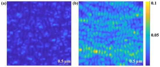
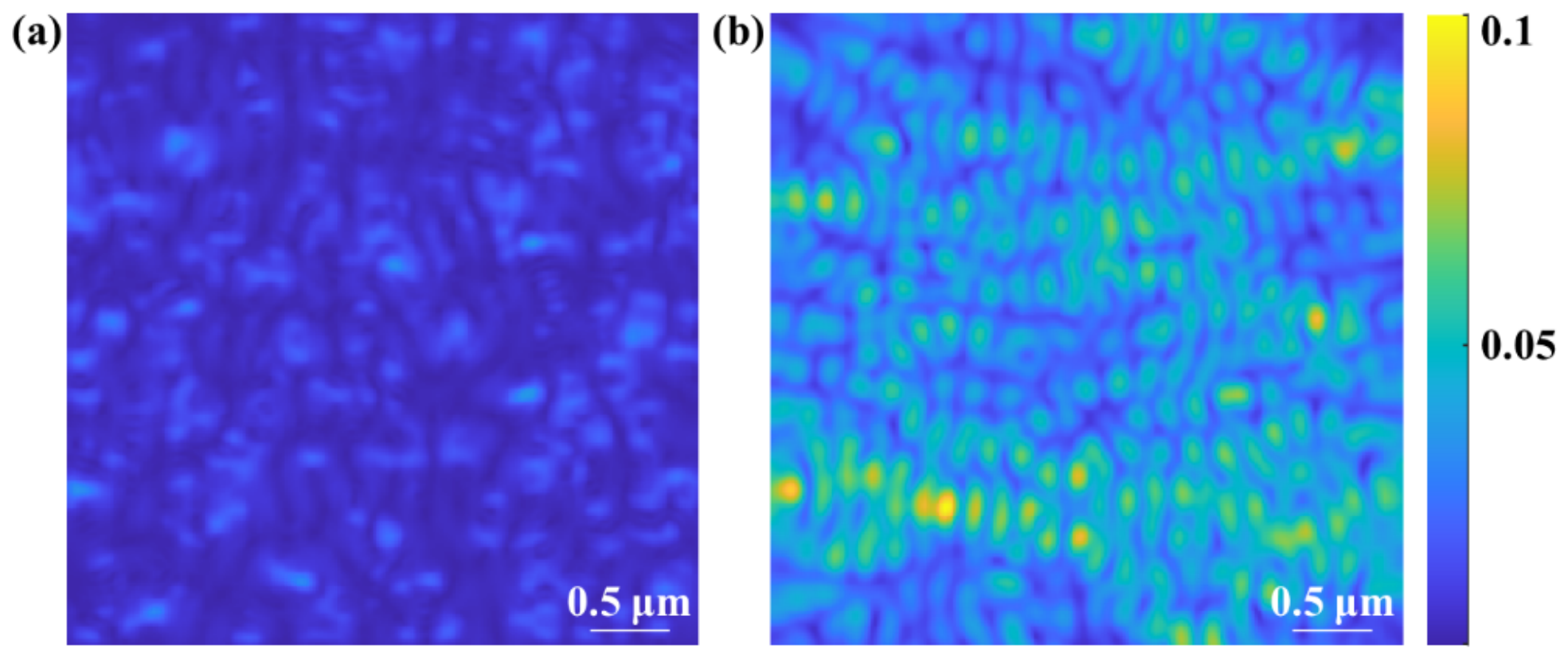
To evaluate roughness-induced background scattering, a metal boundary is imposed at the lower z-boundary to emulate an extreme case of strong reflection from the sample stage. The roughness-induced scattered-field distributions above the Si and 4H-SiC substrates are recorded using a monitor positioned above the source, as shown in Figure 2a and Figure 2b, respectively. Compared with Si, 4H-SiC exhibits substantially stronger background scattering, indicating greater susceptibility to roughness-induced noise.
Figure 2.
Surface electric field distribution caused by surface roughness scattering: (a) Si substrate; (b) 4H-SiC substrate.
Statistical analysis of the electric-field intensity distributions is performed to characterize background noise levels. The mean background intensity and standard deviation for the Si substrate are 0.003 and 0.002, respectively, whereas the corresponding values for 4H-SiC reach 0.018 and 0.011. The mean background intensity of 4H-SiC is approximately six times that of Si and is accompanied by considerably stronger spatial fluctuations. This difference primarily stems from the high optical transmittance of 4H-SiC. As a result, a larger fraction of the incident field can propagate through the substrate, be reflected by the lower boundary, and interact again with the rough surface. This additional interaction enhances the roughness-induced background scattering, thereby degrading the SNR.
3.1.2. Defect Scattering Signals
Under 405 nm illumination, a 100 nm-diameter PSL particle (radius a = 50 nm) resides in the sub-wavelength regime, where its optical response is dominated by the electric dipole moment. The induced electric dipole moment of the particle can be expressed as [33]:
where α0 is the quasi-static polarizability of the particle in a homogeneous background medium, and is the local electric field at the particle location. This local field comprises the incident field and the field reflected from the substrate [34]. When the particle is situated above a planar dielectric half-space, the system response can be described using Green’s functions. The Green’s function can be decomposed into a free-space term and a reflection term arising from the interface, with the latter describing the feedback of the substrate on the particle’s dipole radiation field [35,36,37]. Within the framework of the near-field and quasi-static limits, the magnitude of the reflected contribution is governed primarily by the Fresnel reflection coefficients, which are related to the dielectric contrast between the substrate material and the ambient medium [37]. The dielectric contrast factor can be expressed as [36]:
where and are the relative permittivities of the substrate and the ambient medium (air, = 1), respectively, and is the refractive index of the substrate. At 405 nm, Si exhibits a substantially larger optical contrast with respect to the surrounding medium than 4H-SiC, resulting in stronger substrate-mediated enhancement of the local field near the particle. By contrast, the lower dielectric contrast of 4H-SiC suppresses the local-field enhancement and consequently reduces the particle-scattering signal.
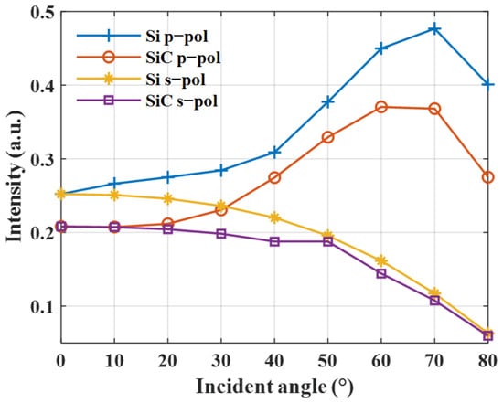
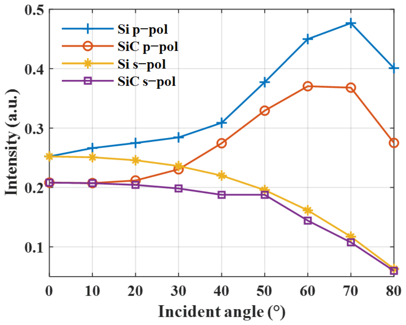
The scattered electric fields of PSL particles positioned on Si and 4H-SiC substrates are calculated using the FDTD method. Both p- and s-polarized illumination are considered, with the incidence angle varied from 0° to 80°. Figure 3 presents the statistical distribution of the near-field intensity. Across the investigated polarization states and incidence angles, the PSL particle on the Si substrate consistently exhibits a stronger electric-field response than that on the 4H-SiC substrate, confirming that the dielectric contrast between the particle and substrate modulates the defect local field. These results indicate that, under identical inspection conditions, nanoscale particles on SiC wafers produce weaker optical signals than those on Si, thereby limiting the achievable detection sensitivity.
Figure 3.
Near-field electric field intensity of PSL particles on Si and SiC substrates.
In summary, the optical properties of 4H-SiC give rise to two concurrent sources of sensitivity degradation in darkfield inspection. First, the high optical transmittance amplifies roughness-induced background scattering, thereby suppressing the SNR. Second, the relatively low dielectric contrast suppresses the defect local field, resulting in attenuated scattering signals. Collectively, these coupled effects increase the difficulty of defect inspection on SiC wafers and impose fundamental limitations on detection sensitivity.
3.2. Detection Optimization Guided by Defect Scattering
3.2.1. Imaging Simulation of Typical Morphological Defects
Based on the dual sensitivity degradation mechanism identified above, namely background enhancement and defect signal attenuation, improving the darkfield inspection performance of SiC requires enhancing the detectable defect-scattering signals while increasing their distinguishability from the background. Since the incidence angle and polarization dependence of defect scattering markedly modulates its spatial distribution and intensity, the imaging behavior of PSL particles and triangular defects is systematically investigated under different illumination conditions. Signal intensity and SNR serve as the key metrics for evaluating the scattering characteristics and guiding the illumination design for 4H-SiC darkfield inspection. The SNR is defined as [38]:
where represents the defect pixel intensity, and and are the mean value and standard deviation of the intensity in the defect-free region, respectively. The defect intensity is taken as the maximum value of the defect signal.
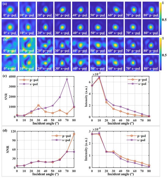
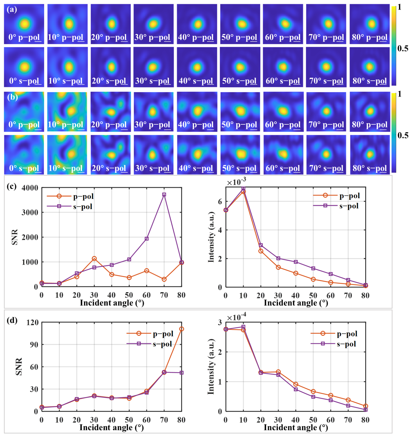
Figure 4a,b present the simulated images of the particle and triangular defects under various incident angles and polarization states. To facilitate the visualization of defect signals, all images are displayed on a normalized intensity scale.
Figure 4.
Simulation results of particles and triangular defects at different incident angles and polarization states: normalized images of (a) the PSL particle and (b) the triangular defect; SNR and signal intensity curves for (c) the PSL particle and (d) the triangular defect. Scale bar: 0.5 μm.
For imaging with an objective of NA = 0.3, the PSL particle remains distinguishable from the roughness background across all investigated illumination conditions. Figure 4c shows the corresponding SNR and signal intensity. At large incidence angles (>40°), the SNR under s-polarized illumination yields a higher SNR than p-polarized illumination, with the maximum occurring at 70°. Moreover, s-polarized illumination produces a stronger particle signal over the entire angular range. These results indicate that highly oblique s-polarized illumination more effectively enhances the detectability of PSL particles.
As shown in Figure 4b, the triangular defect exhibits an extremely low SNR under normal incidence, with its signal obscured by the background noise. Both the SNR and defect contrast increase substantially with increasing incidence angle, as shown in Figure 4d. For incidence angles below 80°, the difference in SNR between s- and p-polarized illumination is not pronounced. The maximum SNR occurs at 70° for s-polarized illumination and at 80° for p-polarized illumination. Notably, at large incidence angles, p-polarized illumination produces a stronger defect signal than s-polarized illumination. This indicates that p-polarized illumination at high oblique angles is more effective in exciting the scattering components of triangular defects.
3.2.2. Detection Performance Analysis
The simulation results demonstrate that nanoscale morphological defects on SiC wafers can be effectively resolved by appropriately tailoring the illumination conditions, even with a low-magnification imaging objective of NA = 0.3. Both defect types exhibit enhanced SNR at large incidence angles. Regarding polarization dependence, distinct response characteristics emerge: particle defects exhibit superior detectability under s-polarization, whereas triangular defects show an advantage under p-polarization.
For inspection scenarios specifically targeting particle defects, an optimized configuration of 70° incidence combined with s-polarized illumination is preferred. However, practical wafer inspection must accommodate multiple defect types while accounting for system complexity and operational stability. A 70° oblique-incidence geometry with tunable polarization therefore provides a robust solution, offering a favorable balance in detection performance across critical defect modes.
It should be emphasized that the simulation framework developed in this study is intended to elucidate the underlying physical mechanisms and guide optimization of the system optical parameters, thereby providing a theoretical basis for high-sensitivity defect inspection. The numerical results are intended for relative performance comparison within the established model rather than for directly predicting the absolute signal intensity or SNR in a practical inspection system. This limitation arises from the inherent differences between idealized simulations and experimental realities. For instance, while PML boundaries suppress non-physical reflections in simulations, practical systems inevitably suffer from stray light, multiple reflections, and scattering by optical components. Consequently, especially for highly transmissive 4H-SiC, the experimentally measured SNR is expected to be lower than the simulated value.
4. Experimental Results
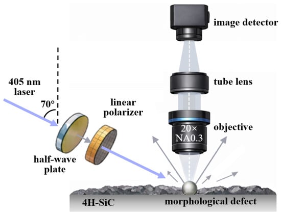
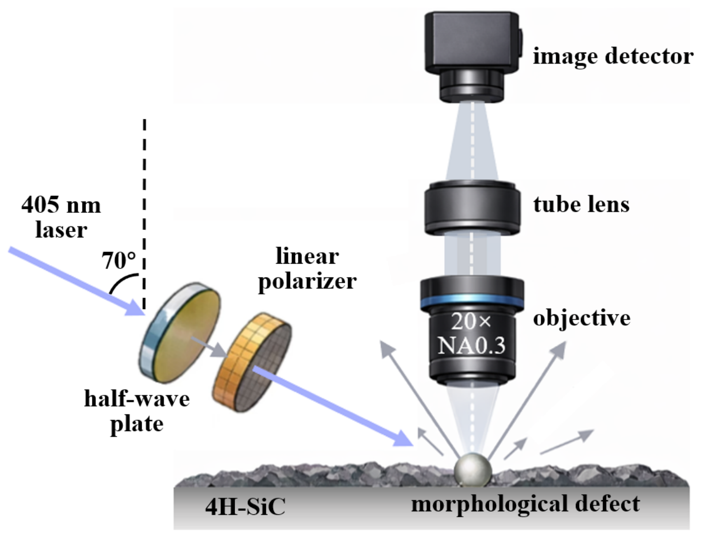
To verify the theoretical predictions, a polarization-tunable laser scattering darkfield imaging system is developed, as shown in Figure 5. A 405 nm laser illuminates the wafer at an incident angle of 70°. A half-wave plate and a linear polarizer are incorporated into the illumination path to enable flexible switching between p- and s-polarization states. On the detection side, a low-magnification, large-field-of-view objective (MPlanApo (95)-20×, 20×/NA 0.3, Kozo, Nanjing, China) with an NA of 0.3 is used to collect the scattered light, thereby improving the defect inspection throughput. Experiments are first conducted on a 4H-SiC wafer deposited with 100 nm PSL particles to evaluate the system’s capability for nanoparticle detection; subsequently, practical step bunching and scratch defects on a SiC wafer are further inspected to assess the applicability of the system for low-contrast morphological defect detection.
Figure 5.
Schematic diagram of the laser scattering darkfield imaging detection system with 70° incidence and tunable polarization.
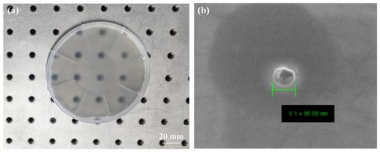
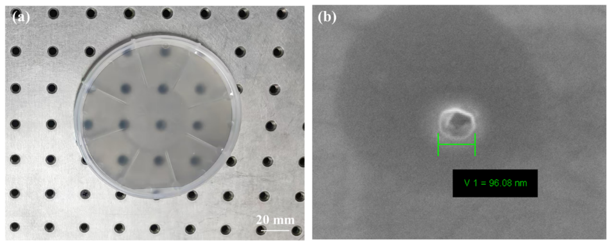
A 4-inch 4H-SiC wafer deposited with nominally 100 nm-diameter PSL particles is used as the test sample, as shown in Figure 6a. The PSL particles are prepared by spin-coating a diluted PSL suspension onto a thoroughly cleaned SiC wafer surface, resulting in a sparse and randomly distributed particle layer. Due to the randomness of particle positions during spin-coating, the exact locations of individual particles cannot be predetermined or independently marked prior to optical inspection. To obtain independent, sample-level confirmation of the deposited PSL particles, SEM characterization is also performed on the same sample. Figure 6b shows a representative SEM image, confirming the presence of a particle with a size and morphology closely consistent with those of the nominal 100 nm PSL particles used in the experiment.
Figure 6.
4H-SiC wafer with spin-coated 100 nm PSL particles: (a) photograph of the 4H-SiC wafer; (b) SEM image of a particle on the wafer.
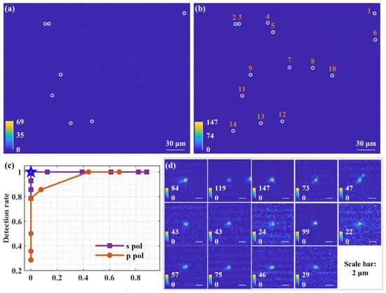
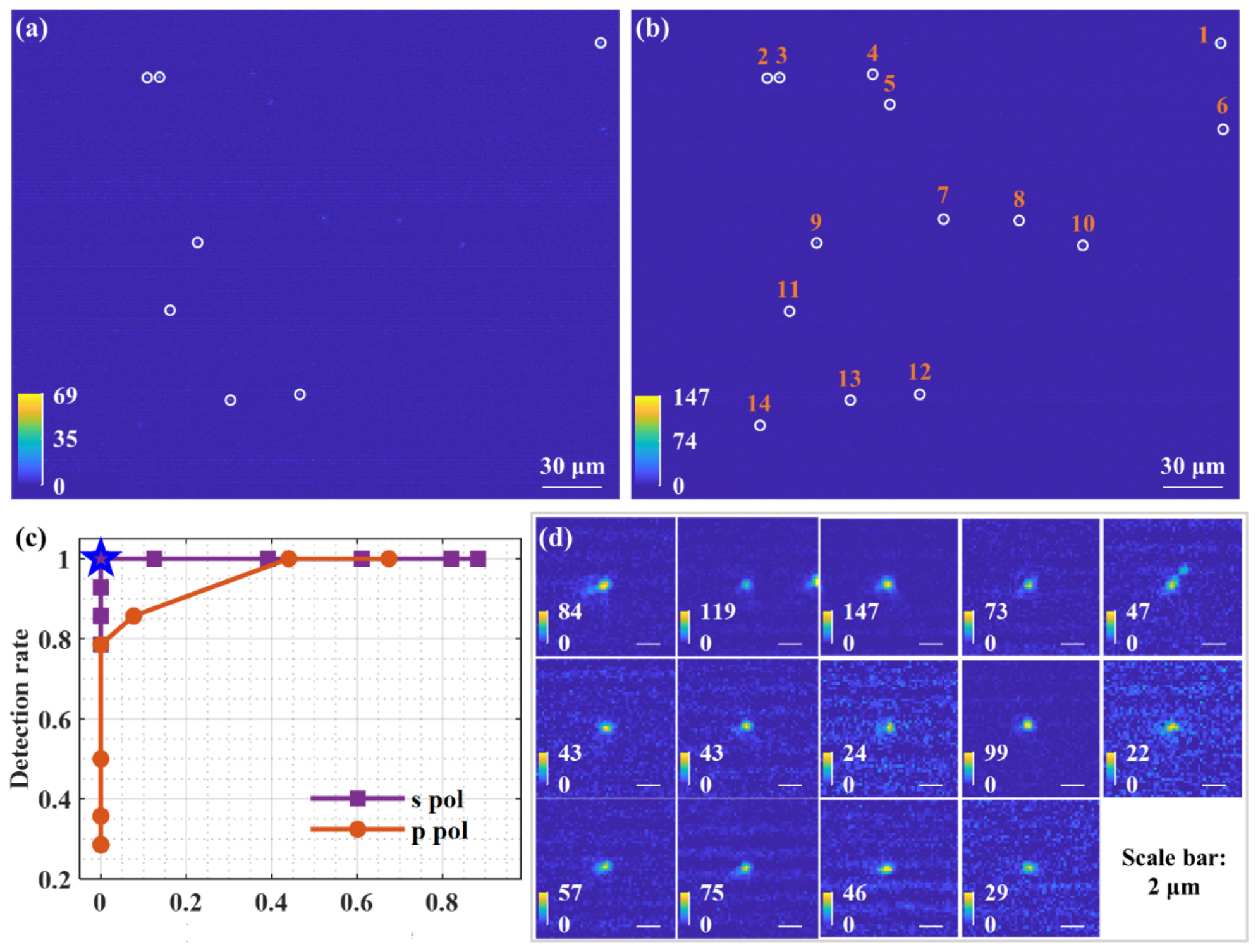
Optical images are acquired under p- and s-polarized illumination while maintaining the same sample position and field-of-view, as shown in Figure 7a and Figure 7b, respectively. The detection performance under the two polarization conditions is evaluated using detection rate–false discovery rate (DR-FDR) curves. The horizontal and vertical axes represent the false discovery rate and detection rate, respectively, as defined by
where TP, FP, and FN denote true-positive detections, false-positive detections, and missed detections, respectively. The DR-FDR curves are constructed by varying the pixel-intensity threshold from 10 to 30 and calculating the corresponding DR and FDR at each threshold. The resulting curves are shown in Figure 7c.
Figure 7.
Detection performance of 100 nm PSL particles under different polarization conditions: (a) p-polarized image; (b) s-polarized image; (c) DR-FDR curves; (d) PSL particle signals in the s-polarized image.
For a consistent quantitative comparison between the two polarization conditions, an intensity threshold of 20 is selected as an example, with pixels above this threshold identified as defect signals. Successfully detected particles are marked by circles in Figure 7a,b. Only 7 particles are detected in the p-polarized image, whereas all 14 particles are detected in the s-polarized image. Table 2 lists the SNR values for each PSL particle labeled in Figure 7b under both polarization conditions. Figure 7d shows the signals of individual PSL particles in the s-polarized image.
Table 2.
SNR values of PSL particles under p- and s-polarized illumination.
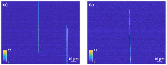
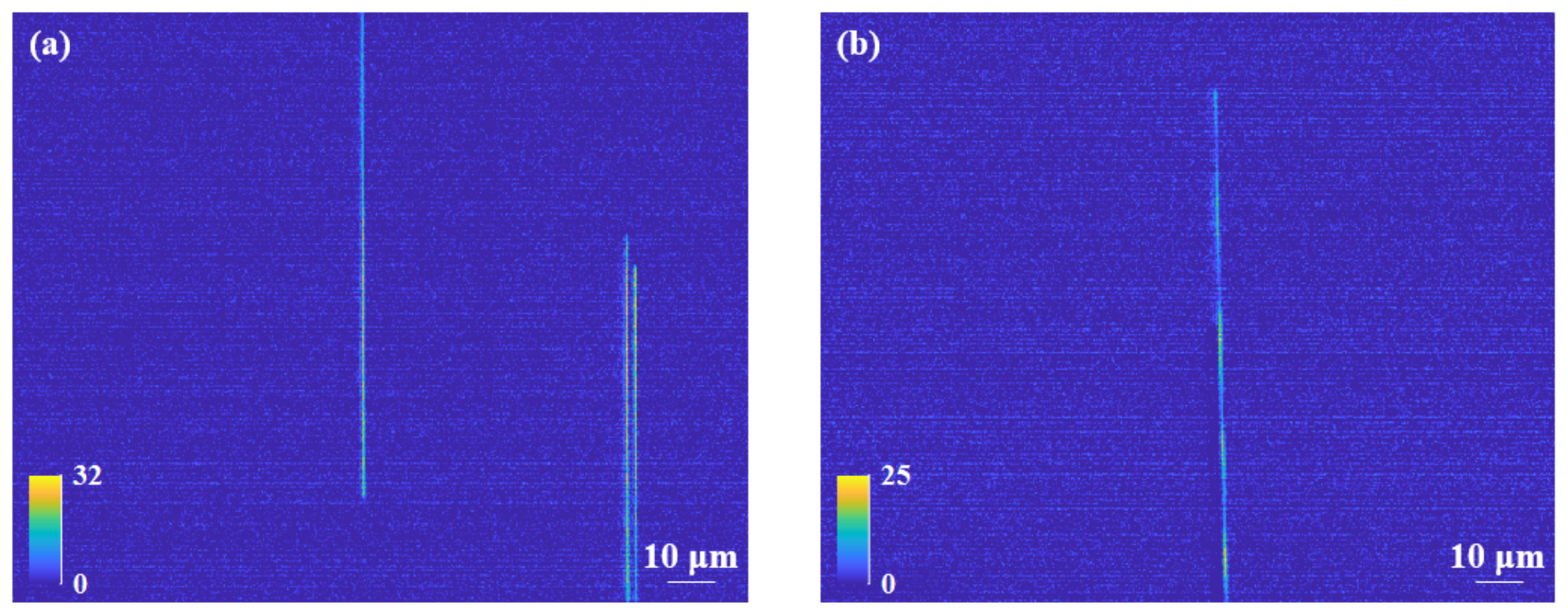
Process-induced morphological defects on a 6-inch 4H-SiC wafer are inspected under s-polarized illumination. Figure 8a and Figure 8b show regions containing a step-bunching defect and a scratch defect, respectively. Step-bunching defects can be induced during epitaxial growth by pre-existing or latent scratches on the substrate surface and typically appear as a series of nearly parallel, step-like stripes. Such defects can degrade the electrical performance and reliability of SiC power devices, particularly metal-oxide-semiconductor field-effect transistors (MOSFETs) [39]. Scratches are generally induced by mechanical stress during wafer slicing, grinding, polishing, or handling. These linearly extended morphological defects can promote the propagation of bulk defects and compromise epitaxial-layer quality. As shown in Figure 8a, the step-bunching defect exhibits a series of approximately parallel striations, whereas the scratch in Figure 8b appears as a continuously extended linear feature. Under s-polarized illumination at an incidence angle of 70°, both defects are clearly distinguishable from the surrounding background, with measured SNR values of 31.832 and 24.485 for the step-bunching and scratch defects, respectively.
Figure 8.
Morphological defects on a SiC wafer: (a) step-bunching defect; (b) scratch defect.
5. Discussion
5.1. Analysis of PSL Particle Detection Performance
Numerical analysis reveals that darkfield inspection of 4H-SiC is constrained by the coupled effects of background enhancement and defect signal attenuation. Meanwhile, the polarization state and incidence angle markedly modulate the defect-scattering response. Among the investigated configurations, 70° oblique incidence exhibits favorable overall performance across different defect types, whereas s-polarized illumination yields a pronounced signal enhancement for 100 nm PSL particles. Theoretical findings directly guide the experimental configuration, in which 70° oblique incidence and polarization-tunable illumination are adopted to improve defect detectability.
As shown in Figure 7a,b, consistent with the simulation results, s-polarized illumination produces stronger scattering signals than p-polarized illumination. The ideal detection condition corresponds to the upper-left corner of the DR-FDR space (FDR = 0 and DR = 1), indicating that all defects are detected without any false alarms. As shown in Figure 7c, the curve for s-polarization lies closer to this optimal point than that for p-polarization, demonstrating improved detection performance under s-polarized illumination. The SNR values listed in Table 2 further support this observation. At most reference locations, the SNR values obtained under s-polarized illumination are substantially higher than those obtained under p-polarized illumination. At the selected intensity threshold of 20, only 7 of the 14 reference locations are detected under p-polarized illumination, whereas all 14 are detected under s-polarized illumination. This demonstrates that polarization control can effectively modulate the scattering response of 100 nm particles and improve their distinguishability from the background.
The PSL particles used for the comparison between p- and s-polarized illumination are identified as follows. Candidate particle signals are first selected according to their localized scattering intensity and are subsequently examined to exclude obvious background fluctuations and surface-related features. Under the current imaging conditions, the pixel distribution and spatial extent of the scattering signals attributed to 100 nm PSL particles are consistent with the expected particle response. In contrast, common surface-related features, such as scratches or contaminants, generally exhibit different spatial morphologies. Based on these criteria, 14 isolated particle-like scattering features are retained as common reference particle locations for both polarization conditions.
In addition, certain variations in scattering intensity among particles are observed in Figure 7d, which are mainly attributed to differences in particle diameter, adhesion state, and local roughness. Nevertheless, most particles maintain high contrast against the background, demonstrating the reliability of the system configuration for detecting nanoscale particulate defects on SiC wafers.
5.2. Selection of Defect Types
It should be noted that the numerical simulations in this study employ idealized defect models, such as spherical particles and simplified triangular cross-section defects, to elucidate the fundamental scattering mechanisms and optimize the system detection performance. However, morphological defects formed during practical SiC wafer processing and epitaxial growth generally exhibit more complex geometries. In addition, spatially extended defects with small characteristic linewidths often show low contrast under conventional optical microscopy and are therefore difficult to detect. Based on these considerations, targets with different spatial scales and morphological characteristics are selected for experimental validation. The 100 nm PSL particles represent localized subwavelength point scatterers and are used to evaluate the detection sensitivity for nanoscale particles, whereas step-bunching and scratch defects represent practical SiC wafer inspection scenarios with low-contrast, spatially extended morphological defects. Although practical defects differ geometrically from idealized models, the theoretically derived modulation strategy enables high-SNR defect detection on SiC wafers, highlighting the potential of the proposed system for wafer-quality screening.
6. Conclusions
In conclusion, this study investigates the physical mechanisms limiting the sensitivity of darkfield scattering inspection of nanoscale morphological defects on SiC wafers from the perspective of material properties. Compared with Si, the high transmittance of 4H-SiC wafers amplifies roughness-induced background scattering, while the relatively low dielectric contrast weakens defect scattering signals, leading to a dual sensitivity degradation mechanism characterized by concurrent background enhancement and defect signal attenuation. Based on the polarization- and incidence-angle-dependent scattering behavior of defects, an illumination configuration combining 70° oblique incidence with tunable polarization is established. With s-polarized illumination and low-NA imaging, the developed system detects all 100 nm PSL particles and effectively identifies practical step-bunching and scratch defects on the 4H-SiC wafer, demonstrating its applicability to both point-like and extended topographic depression-type defects. This work establishes a mechanism-driven framework linking physical understanding with inspection optimization, providing an extensible approach for enhancing the discriminability of subtle defects in wide-bandgap semiconductors.
Author Contributions
Conceptualization, J.H.; methodology, H.L.; validation, Y.H. and Y.S.; formal analysis, Z.H.; investigation, G.Z.; supervision, T.L.; data curation, X.X. and R.X.; writing—original draft preparation, J.H.; writing—review and editing, M.Z.; project administration, S.Z.; resources, N.Y. and B.M. All authors have read and agreed to the published version of the manuscript.
Funding
This work was supported by Science and Technology Program of the State Administration for Market Regulation of China (2024MK27), National Major Science and Technology Project (2024ZD0708101), National Natural Science Foundation of China (52305584), Key Research and Development Project of Henan Province (231111220500), and Shaanxi Qinchuangyuan “Scientist + Engineer” Team Building Project (2024QCY-KXJ-018).
Data Availability Statement
The data supporting the findings of this study are available from the corresponding authors upon reasonable request.
Acknowledgments
The authors would like to thank Wei Li of the National Institute of Metrology, China, for providing the test samples.
Conflicts of Interest
The authors declare no conflicts of interest.
References
- Wang, R.; Huang, Y.C.; Yang, D.R.; Pi, X.D. Impurities and defects in 4H silicon carbide. Appl. Phys. Lett. 2023, 122, 180501. [Google Scholar] [CrossRef] [Scilit]
- Ravindran, R.; Massoud, A.M. An overview of wide and ultra-wide bandgap semiconductors for next-generation power electronics applications. Microelectron. Eng. 2025, 299, 112348. [Google Scholar] [CrossRef] [Scilit]
- Kimoto, T. Material science and device physics in SiC technology for high-voltage power devices. Jpn. J. Appl. Phys. 2015, 54, 040103. [Google Scholar] [CrossRef] [Scilit]
- Chen, P.; Miao, W.; Ahmed, T.; Pan, Y.; Lin, C.; Chen, S.; Kuo, H.; Tsui, B.; Lien, D. Defect inspection techniques in SiC. Nanoscale Res. Lett. 2022, 17, 30. [Google Scholar] [CrossRef] [Scilit]
- Hu, S.; Liu, Y.; Cheng, Q.; Chen, Z.; Tong, X.; Raghothamachar, B.; Dudley, M. Investigation of defect formation at the early stage of PVT-grown 4H-SiC crystals. J. Cryst. Growth 2024, 628, 127542. [Google Scholar] [CrossRef] [Scilit]
- Kimoto, T.; Watanabe, H. Defect engineering in SiC technology for high-voltage power devices. Appl. Phys. Express 2020, 13, 120101. [Google Scholar] [CrossRef] [Scilit]
- Kimoto, T.; Miyamoto, N.; Matsunami, H. Performance-limiting surface defects in SiC epitaxial p-n junction diodes. IEEE Trans. Electron Devices 1999, 46, 471. [Google Scholar] [CrossRef]
- Rafighdoost, J.; Kolenov, D.; Pereira, S.F. Coherent Fourier scatterometry for detection of killer defects on silicon carbide samples. IEEE Trans. Semicond. Manuf. 2024, 37, 124. [Google Scholar] [CrossRef] [Scilit]
- Ma, P.; Ni, J.; Sun, J.; Li, J.; Chen, H. Three-dimensional detection and quantification of defects in SiC by optical coherence tomography. Appl. Opt. 2020, 59, 1746. [Google Scholar] [CrossRef] [Scilit]
- Harada, S.; Murayama, K. Advances in defect characterization techniques using polarized light observation in SiC wafers for power devices. J. Cryst. Growth 2025, 650, 127982. [Google Scholar] [CrossRef] [Scilit]
- Murayama, K.; Mizutani, S.; Mizutani, Y.; Harada, S. Polarized light observation of semiconductor wafers for power devices. In Proceedings of the 2022 IEEE International Meeting for Future of Electron Devices, Kyoto, Japan, 28–30 November 2022; p. 1. [Google Scholar]
- Wang, X.; Wang, J.; Qin, Z.; Liu, N.; Huang, Y.; Shao, W. Oblique-incidence line confocal imaging with adjustable aperture for wafer defect detection. Measurement 2026, 260, 119875. [Google Scholar] [CrossRef] [Scilit]
- Nishihara, Y.; Kamei, K.; Shiomi, D.; Momose, K. Evaluation of defects in a SiC substrate using the photoluminescence measurement method. Mater. Sci. Forum 2022, 1062, 268. [Google Scholar] [CrossRef] [Scilit]
- Chikvaidze, G.; Mironova-Ulmane, N.; Plaude, A.; Sergeev, O. Investigation of silicon carbide polytypes by Raman spectroscopy. Latv. J. Phys. Tech. Sci. 2014, 51, 51. [Google Scholar] [CrossRef] [Scilit]
- Li, X.; Feng, S.; Chen, W.; Jin, Z.; Chen, Q.; Zuo, C. Adaptive structured-light 3D surface imaging with cross-domain learning. Laser Photonics Rev. 2025, 19, 2401609. [Google Scholar] [CrossRef] [Scilit]
- Tang, L.; Han, M.; Yang, S.; Sun, Y.; Qiu, L.; Zhao, W. High-precision large-aperture single-frame interferometric surface profile measurement method based on deep learning. Int. J. Extrem. Manuf. 2025, 7, 055601. [Google Scholar] [CrossRef] [Scilit]
- Zhang, Z.; Wang, Y.; Yao, C.; Huang, H.; Ma, R.; Du, X.; Zhang, W.; Shi, Z.; Chen, M.; Yan, T.; et al. 3D surface profiling via direct end-to-end regression with a photonic geometric sensor. Laser Photonics Rev. 2026, 20, e02158. [Google Scholar] [CrossRef] [Scilit]
- Chen, H.; Shao, C.; Chen, X.; Li, X.; Yang, X.; Xie, X.; Li, M.; Wang, D.; Xu, X. Surface damage to a 4H-SiC single-crystal substrate caused by dual-fluid spray cleaning. Appl. Surf. Sci. 2025, 709, 163868. [Google Scholar] [CrossRef] [Scilit]
- Grundmann, J.; Bodermann, B.; Ermilova, E.; Weise, M.; Hertwig, A.; Klapetek, P.; Rafighdoost, J.; Pereira, S. Optical and tactile measurements on SiC sample defects. J. Sens. Sens. Syst. 2024, 13, 109–121. [Google Scholar] [CrossRef] [Scilit]
- Ermilova, E.; Weise, M.; Hertwig, A. Application of imaging ellipsometry and white light interference microscopy for detection of defects in epitaxially grown 4H-SiC layers. J. Eur. Opt. Soc.-Rapid Publ. 2023, 19, 23. [Google Scholar] [CrossRef] [Scilit]
- Hu, J.; Liu, T.; Ji, P.; Zhang, G.; Huang, Y.; Cheung, C.; Yang, S. High-sensitivity, high-throughput inspection of nanoscale defects using a laser confocal positioning-assisted dark-field imaging system. Opt. Laser Technol. 2025, 191, 113269. [Google Scholar] [CrossRef] [Scilit]
- Hu, J.; Huang, Y.; Liu, T.; Wang, W.; Li, W.; Ye, G.; Cheung, C.; Zhan, B.; Yang, S. Azimuth-guided image fusion method for sub-λ/18 defect inspection using a laser scattering dark-field imaging system. Opt. Express 2026, 34, 368. [Google Scholar] [CrossRef] [Scilit]
- Shin, H.; Shin, D. Simulation-assisted image analysis for high-sensitivity detection of 30 nm particles in non-patterned wafer inspection systems. Photonics 2026, 13, 673. [Google Scholar] [CrossRef] [Scilit]
- Taflove, A. Application of the finite-difference time-domain method to sinusoidal steady-state electromagnetic penetration problems. IEEE Trans. Electromagn. Compat. 1980, 22, 191. [Google Scholar] [CrossRef] [Scilit]
- Matsuhata, H.; Sugiyama, N.; Chen, B.; Yamashita, T.; Hatakeyama, T.; Sekiguchi, T. Surface defects generated by intrinsic origins on 4H-SiC epitaxial wafers observed by scanning electron microscopy. Microscopy 2017, 66, 103. [Google Scholar] [CrossRef] [Scilit]
- Guo, J.; Yang, Y.; Raghothamachar, B.; Kim, T.; Dudley, M.; Kim, J. Understanding the microstructures of triangular defects in 4H-SiC homoepitaxy. J. Cryst. Growth 2017, 480, 119. [Google Scholar] [CrossRef] [Scilit]
- Galpin, T.; Chartier, R.; Levergood, N. Refractive index retrievals for polystyrene latex spheres in the spectral range 220–420 nm. Aerosol Sci. Technol. 2017, 51, 1158. [Google Scholar] [CrossRef] [Scilit]
- Deng, Q.; Zhao, Z.; Lin, H.; Liu, L.; Li, X.; Luo, X. System design for dark-field detection of nanoparticles on wafer metal surface. Chin. J. Lasers 2024, 50, 2204003. [Google Scholar]
- Foreman, M.R.; Török, P. Computational methods in vectorial imaging. J. Mod. Opt. 2011, 58, 339. [Google Scholar] [CrossRef] [Scilit]
- Wang, S.; Zhan, M.; Wang, G.; Xuan, H.; Zhang, W.; Liu, C.; Xu, C.; Liu, Y.; Wei, Z.; Chen, X. 4H-SiC: A new nonlinear material for mid-infrared lasers. Laser Photonics Rev. 2013, 7, 831. [Google Scholar] [CrossRef] [Scilit]
- RefractiveIndex INFO. Refractive Index of SiC (Silicon Carbide)—Wang-4H-e. 2013. Available online: https://refractiveindex.info/?shelf=mainbook=SiCpage=Wang-4H-e (accessed on 27 March 2026).
- Available online: https://optics.ansys.com/hc/en-us/articles/360034405354-transmission-Script-command (accessed on 25 September 2026).
- Tzarouchis, D.; Sihvola, A. Light scattering by a dielectric sphere: Perspectives on the Mie resonances. Appl. Sci. 2018, 8, 184. [Google Scholar] [CrossRef] [Scilit]
- Arnoldus, H. Giant dipole moment induced by an interface. Phys. Lett. A 2021, 388, 127044. [Google Scholar] [CrossRef] [Scilit]
- Li, L.; Leong, M.; Kooi, P.; Yeo, T. Spheroidal vector wave eigenfunction expansion of dyadic Green’s functions for a dielectric spheroid. IEEE Trans. Antennas Propag. 2001, 49, 645. [Google Scholar] [CrossRef]
- Xu, Z. Electrostatic interaction in the presence of dielectric interfaces and polarization-induced like-charge attraction. Phys. Rev. E 2013, 87, 013307. [Google Scholar] [CrossRef] [Scilit]
- Cho, M.; Cai, W. Efficient and accurate computation of electric field dyadic Green’s functions in layered media. J. Sci. Comput. 2017, 71, 1319. [Google Scholar] [CrossRef] [Scilit]
- Lee, B.; Chin, S.; Cho, D.; Song, C.; Yeo, J.; Some, D.; Reinhorn, S. Optical characterization of defects on patterned wafers: Exploring light polarization. In Proceedings of the SPIE, Metrology, Inspection, and Process Control for Microlithography XVIII, Santa Clara, CA, USA, 23–26 February 2004; Volume 5375, p. 849. [Google Scholar]
- Isshiki, T.; Hasegawa, M.; Sato, T.; Kobayashi, K.; Miyaki, A.; Iyoki, M.; Yamaoka, T.; Onuki, K. Observation of a latent scratch on chemo-mechanical polished 4H-SiC wafer by mirror projection electron microscopy. Mater. Sci. Forum 2018, 924, 543. [Google Scholar] [CrossRef] [Scilit]

Disclaimer/Publisher’s Note: The statements, opinions and data contained in all publications are solely those of the individual author(s) and contributor(s) and not of MDPI and/or the editor(s). MDPI and/or the editor(s) disclaim responsibility for any injury to people or property resulting from any ideas, methods, instructions or products referred to in the content. |
© 2026 by the authors. Licensee MDPI, Basel, Switzerland. This article is an open access article distributed under the terms and conditions of the Creative Commons Attribution (CC BY) license.